EP4187287A2 - Area array detector, detection method and corresponding container/vehicle inspection system - Google Patents
Area array detector, detection method and corresponding container/vehicle inspection system Download PDFInfo
- Publication number
- EP4187287A2 EP4187287A2 EP22209595.2A EP22209595A EP4187287A2 EP 4187287 A2 EP4187287 A2 EP 4187287A2 EP 22209595 A EP22209595 A EP 22209595A EP 4187287 A2 EP4187287 A2 EP 4187287A2
- Authority
- EP
- European Patent Office
- Prior art keywords
- detector
- area array
- assembly
- assemblies
- detection data
- Prior art date
- Legal status (The legal status is an assumption and is not a legal conclusion. Google has not performed a legal analysis and makes no representation as to the accuracy of the status listed.)
- Granted
Links
Images



Classifications
-
- G—PHYSICS
- G01—MEASURING; TESTING
- G01V—GEOPHYSICS; GRAVITATIONAL MEASUREMENTS; DETECTING MASSES OR OBJECTS; TAGS
- G01V5/00—Prospecting or detecting by the use of ionising radiation, e.g. of natural or induced radioactivity
- G01V5/20—Detecting prohibited goods, e.g. weapons, explosives, hazardous substances, contraband or smuggled objects
- G01V5/22—Active interrogation, i.e. by irradiating objects or goods using external radiation sources, e.g. using gamma rays or cosmic rays
-
- G—PHYSICS
- G01—MEASURING; TESTING
- G01N—INVESTIGATING OR ANALYSING MATERIALS BY DETERMINING THEIR CHEMICAL OR PHYSICAL PROPERTIES
- G01N23/00—Investigating or analysing materials by the use of wave or particle radiation, e.g. X-rays or neutrons, not covered by groups G01N3/00 – G01N17/00, G01N21/00 or G01N22/00
- G01N23/02—Investigating or analysing materials by the use of wave or particle radiation, e.g. X-rays or neutrons, not covered by groups G01N3/00 – G01N17/00, G01N21/00 or G01N22/00 by transmitting the radiation through the material
- G01N23/04—Investigating or analysing materials by the use of wave or particle radiation, e.g. X-rays or neutrons, not covered by groups G01N3/00 – G01N17/00, G01N21/00 or G01N22/00 by transmitting the radiation through the material and forming images of the material
- G01N23/046—Investigating or analysing materials by the use of wave or particle radiation, e.g. X-rays or neutrons, not covered by groups G01N3/00 – G01N17/00, G01N21/00 or G01N22/00 by transmitting the radiation through the material and forming images of the material using tomography, e.g. computed tomography [CT]
-
- G—PHYSICS
- G01—MEASURING; TESTING
- G01T—MEASUREMENT OF NUCLEAR OR X-RADIATION
- G01T1/00—Measuring X-radiation, gamma radiation, corpuscular radiation, or cosmic radiation
- G01T1/29—Measurement performed on radiation beams, e.g. position or section of the beam; Measurement of spatial distribution of radiation
- G01T1/2914—Measurement of spatial distribution of radiation
- G01T1/2985—In depth localisation, e.g. using positron emitters; Tomographic imaging (longitudinal and transverse section imaging; apparatus for radiation diagnosis sequentially in different planes, steroscopic radiation diagnosis)
-
- G—PHYSICS
- G01—MEASURING; TESTING
- G01T—MEASUREMENT OF NUCLEAR OR X-RADIATION
- G01T1/00—Measuring X-radiation, gamma radiation, corpuscular radiation, or cosmic radiation
- G01T1/16—Measuring radiation intensity
- G01T1/20—Measuring radiation intensity with scintillation detectors
- G01T1/2018—Scintillation-photodiode combinations
-
- G—PHYSICS
- G01—MEASURING; TESTING
- G01V—GEOPHYSICS; GRAVITATIONAL MEASUREMENTS; DETECTING MASSES OR OBJECTS; TAGS
- G01V5/00—Prospecting or detecting by the use of ionising radiation, e.g. of natural or induced radioactivity
- G01V5/20—Detecting prohibited goods, e.g. weapons, explosives, hazardous substances, contraband or smuggled objects
-
- G—PHYSICS
- G01—MEASURING; TESTING
- G01V—GEOPHYSICS; GRAVITATIONAL MEASUREMENTS; DETECTING MASSES OR OBJECTS; TAGS
- G01V5/00—Prospecting or detecting by the use of ionising radiation, e.g. of natural or induced radioactivity
- G01V5/20—Detecting prohibited goods, e.g. weapons, explosives, hazardous substances, contraband or smuggled objects
- G01V5/22—Active interrogation, i.e. by irradiating objects or goods using external radiation sources, e.g. using gamma rays or cosmic rays
- G01V5/226—Active interrogation, i.e. by irradiating objects or goods using external radiation sources, e.g. using gamma rays or cosmic rays using tomography
-
- G—PHYSICS
- G01—MEASURING; TESTING
- G01N—INVESTIGATING OR ANALYSING MATERIALS BY DETERMINING THEIR CHEMICAL OR PHYSICAL PROPERTIES
- G01N2223/00—Investigating materials by wave or particle radiation
- G01N2223/50—Detectors
- G01N2223/501—Detectors array
Definitions
- This disclosure relates to the field of ray scanning, and particularly, to an area array detector for a container/vehicle inspection system, the container/vehicle inspection system using the area array detector, and a corresponding detection method.
- detectors for DR Digital Radiography
- CT Computer Tomography
- the detectors for DR scanning are in fewer detector rows, and the rows of detectors are arranged continuously.
- the detectors for CT scanning are in a small overall size, and rows of detectors use the same scintillator. Each kind of detector equipment supports one scanning mode.
- an area array detector for a container/vehicle inspection system which through a backplane carries a plurality of sparsely arranged detector assemblies, wherein a first detector assembly is different from other second detector assemblies. Detection data of the first detector assembly or detection data of all the detector assemblies can be outputted according to needs of scanning modes, for imaging in a corresponding scanning mode, thereby the area array detector supporting the plurality of scanning modes is enabled.
- an area array detector for a container/vehicle inspection system comprising: a plurality of sparsely arranged detector assemblies, wherein a first detector assembly is different from other second detector assemblies; and a backplane for carrying and mounting the plurality of detector assemblies.
- the first detector assembly and the second detector assembly have different scintillator arrays.
- the scintillator arrays of the first detector assembly and the second detector assembly differ in at least one of a pixel size or material.
- a preset number of adjacently arranged detector assemblies are disposed inside one detector housing to form one independent detector unit with an all-sealed structure, the detector unit being seal mounted with the backplane.
- the preset number comprises 2.
- the area array detector further comprises: a filler assembly, wherein the filler assembly and a detector assembly arranged adjacent to the filler assembly are disposed inside one detector housing to form one independent detector unit with an all-sealed structure, the detector unit being seal mounted with the backplane.
- the backplane is a planar backplane or a curved backplane.
- the plurality of detector assemblies are arranged on a curved surface of the curved backplane, so that detection sensitive surfaces of the plurality of detector assemblies are curved and aligned with a ray source located in a central area of the curved surface.
- a first pixel size of the scintillator array of the first detector assembly is less than a second pixel size of the scintillator array of the second detector assembly.
- a plurality of the area array detectors are spliced into a larger area array detector.
- the area array detector further comprises: a data acquisition circuit board configured to acquire detection data of the plurality of detector assemblies, and according to different scanning modes, output the detection data of the first detector assembly or the detection data of all the detector assemblies for imaging in a corresponding scanning mode.
- the data acquisition circuit board is configured to output the detection data of the first detector assembly for DR imaging in a digital radiography DR scanning mode, and output the detection data of all the detector assemblies for CT imaging in a computed tomography CT scanning mode.
- a container/vehicle inspection system comprising the area array detector.
- a detection method comprising:
- the detection data of the first detector assembly is output for DR imaging
- the detection data of all the detector assemblies is output for CT imaging
- the DR scanning mode is performed first, and is switched to the CT scanning mode when a suspicious substance difficult to distinguish is found.
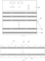
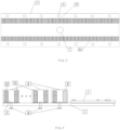
- Fig. 1 illustrates a front view of an area array detector according to some embodiments of the present disclosure.
- Fig. 2 illustrates a side view of an area array detector according to some embodiments of the present disclosure.
- the area array detector of this embodiment comprises, for example: a data acquisition circuit board 1, a backplane 2, a plurality of sparsely arranged detector assemblies 3, and the like.
- the backplane 2 is used for carrying and mounting the plurality of detector assemblies 3 and the data acquisition circuit board 1.
- the number of the detector assemblies and a space between different detector assemblies can be configured and adjusted according to actual business needs.
- a first detector assembly 32 is different from other second detector assemblies 31, for example, they have different scintillator arrays.
- the scintillator arrays of the first detector assembly 32 and each second detector assembly 31 differ in at least one of a pixel size or material.
- the first detector assembly 32 comprises a scintillator array in a first pixel size and a matched optoelectronic device
- the second detector assembly 31 comprises a scintillator array in a second pixel size and a matched optoelectronic device, wherein the first pixel size is less than the second pixel size, for example, the first pixel size is 1/4 of the second pixel size, so that imaging with higher resolution is achieved by using a detector assembly in the smaller pixel size.
- the scintillator array of the first detector assembly 32 is, for example, a GAGG (Gadolinium Aluminum Gallium Garnet) scintillator array.
- the scintillator array of the second detector assembly 31 is, for example, a cesium iodide scintillator array.
- Fig. 3 illustrates a schematic diagram of the first detector assembly 32 being located in a first row, however, it is appreciated that the arrangement location of the first detector assembly 32 is not limited in the present disclosure.
- a preset number for example, two
- the detector unit 5 is also seal mounted with the backplane 2 through a screw hole 7 with a sealed structure by using a screw 8.
- the sealed structure makes the scintillator array, photodiodes and related electronic devices in the detector unit 5 isolated from water, air, smoke, fog, and the like in a use environment, which can improve the reliability of the area array detector, so that the area array detector can reliably operate for a long time in a place such as a coastal port and the like.
- the detector unit 5 has an independent sealed structure, and can be added, reduced or replaced without affecting the function of the whole area array detector, and can be assembled into different structures to be applied to different business system needs, so that it is more flexible and economical in production and manufacturing.
- the area array detector further comprises a filler assembly 9, the filler can be a lighter substance such as plastic.
- the filler assembly 9 and a detector assembly 3 arranged adjacent to the filler assembly are disposed inside one detector housing 4 to form one independent detector unit 5 with an all-sealed structure, the detector unit 5 being also seal mounted with the backplane 2. If two detector assemblies 3 adjacently arranged and the detector housing 4 thereof form one independent detector unit 5 with the all-sealed structure, when the number of the detector assemblies 3 is odd, one filler assembly 9 can be provided, and the filler assembly 9 and a detector assembly 3 arranged adjacent to the filler assembly are disposed inside one detector housing 4 to form one independent detector unit 5 with the all-sealed structure.
- a multi-channel current input analog-to-digital converter can also be included, for acquiring and digitizing a detection signal from each detector assembly 3.
- the backplanes 2 shown in the foregoing embodiments are all planar backplanes, but the backplane 2 can also be a curved backplane.
- the backplane 2 is a curved backplane
- the plurality of detector assemblies 31 and 32 are arranged on a curved surface of the curved backplane, and detection sensitive surfaces of the plurality of detector assemblies 31 and 32 are curved and aligned with a ray source located in a central area of the curved surface. This makes ray beams directly irradiated to a pixel center of each detection crystal, so that scattering crosstalk is reduced, and imaging quality is improved.
- the data acquisition circuit board 1 is configured to acquire detection data of the plurality of detector assemblies, and according to different scanning modes, output the detection data of the first detector assembly 32 or the detection data of all the detector assemblies 3 for imaging in a corresponding scanning mode.
- the data acquisition circuit board 1 is configured to output the detection data of the first detector assembly 32 for DR imaging in a DR scanning mode, which can achieve fast high-quality imaging and can be used for higher-speed scanning, and output the detection data of all the detector assemblies for CT imaging in a CT scanning mode, which can obtain more detection data in a shorter scanning time.
- the scanning mode can be switched according to business needs. For example, the DR scanning is performed first, and when there is a suspicious substance difficult to distinguish in an image, the scanning is switched to the CT mode, to reconstruct the image and find a more detailed substance structure. Therefore, the functions of two sets of equipment can be realized by one set of equipment, which can select the working mode according to characteristics of a detected object, and can also simultaneously check and analyze the detected object from two dimensions and three dimensions, to acquire more comprehensive substance information from different dimensions, so that it has a higher substance identification capability.
- the data acquisition circuit board 1 is further configured to process the detection data of the first detector assembly 32 and the second detector assembly 31 into the same pixel size by pixel division or pixel combination, before outputting the detection data of all the detector assemblies.
- every 4 pixels corresponding to the detection data of the first detector assembly 32 can be combined into 1 pixel for output, such that it is consistent in size with each pixel corresponding to the detection data of the second detector assembly 31, thereby maintaining the integrity of the CT imaging data, and making the imaging clearer because of the small pixel size when the DR imaging outputs the pixels alone.
- the data acquisition circuit board 1 can be implemented, for example, based on an FPGA (Field Programmable Gate Array) or other programmable devices.
- FPGA Field Programmable Gate Array
- a plurality of the area array detectors can also be used in combination, and the plurality of the area array detectors are spliced into a larger area array detector. As shown in Fig. 8 , the plurality of the area array detectors are horizontally and seamlessly arranged to form an area array with a sufficient length. Therefore, the detection is jointly performed, to obtain more detection data in a shorter scanning time, so as to have a higher substance identification capability.
- the area array detectors in the above embodiments or a combination thereof can be used in a large product such as a container/vehicle inspection system, for example, CT/DR inspection equipment for an X/Gamma ray container/vehicle. That is, the container/vehicle inspection system comprises the area array detectors in the above embodiments or the combination thereof. In addition to the area array detectors or the combination thereof, the container/vehicle inspection system can further comprise an accelerator for generating an X ray or Gamma ray with a certain dose and a certain energy, and an image acquisition device for converting an electrical signal output from the area array detector into a digital image signal.
- an accelerator for generating an X ray or Gamma ray with a certain dose and a certain energy
- an image acquisition device for converting an electrical signal output from the area array detector into a digital image signal.
- a corresponding detection method comprising: acquiring detection data of a plurality of sparsely arranged detector assemblies, wherein a first detector assembly in the plurality of detector assemblies is different from other second detector assemblies(S91); and according to different scanning modes, outputting the detection data of the first detector assembly or the detection data of all the detector assemblies for imaging in a corresponding scanning mode(S92).
- the detection data of the first detector assembly is output for DR imaging
- the detection data of all the detector assemblies is output for CT imaging.
- the scanning mode can be switched according to business needs. For example, the DR scanning is performed first, and is switched to the CT mode for scanning when there is a suspicious substance difficult to distinguish in an image.
Landscapes
- Physics & Mathematics (AREA)
- Life Sciences & Earth Sciences (AREA)
- General Physics & Mathematics (AREA)
- High Energy & Nuclear Physics (AREA)
- Health & Medical Sciences (AREA)
- Geophysics (AREA)
- General Life Sciences & Earth Sciences (AREA)
- Molecular Biology (AREA)
- Spectroscopy & Molecular Physics (AREA)
- Radiology & Medical Imaging (AREA)
- General Health & Medical Sciences (AREA)
- Nuclear Medicine, Radiotherapy & Molecular Imaging (AREA)
- Immunology (AREA)
- Analytical Chemistry (AREA)
- Biochemistry (AREA)
- Chemical & Material Sciences (AREA)
- Pulmonology (AREA)
- Pathology (AREA)
- Theoretical Computer Science (AREA)
- Engineering & Computer Science (AREA)
- Analysing Materials By The Use Of Radiation (AREA)
- Measurement Of Radiation (AREA)
- Geophysics And Detection Of Objects (AREA)
Abstract
Description
- The present disclosure is based on and claims priority of
Chinese application for invention No.202111422301.X, filed on November 26, 2021 - This disclosure relates to the field of ray scanning, and particularly, to an area array detector for a container/vehicle inspection system, the container/vehicle inspection system using the area array detector, and a corresponding detection method.
- In the related art, there are detectors for DR (Digital Radiography) scanning, and also detectors for CT (Computed Tomography) scanning. The detectors for DR scanning are in fewer detector rows, and the rows of detectors are arranged continuously. The detectors for CT scanning are in a small overall size, and rows of detectors use the same scintillator. Each kind of detector equipment supports one scanning mode.
- In embodiments of the present disclosure, there is provided an area array detector for a container/vehicle inspection system, which through a backplane carries a plurality of sparsely arranged detector assemblies, wherein a first detector assembly is different from other second detector assemblies. Detection data of the first detector assembly or detection data of all the detector assemblies can be outputted according to needs of scanning modes, for imaging in a corresponding scanning mode, thereby the area array detector supporting the plurality of scanning modes is enabled.
- In some embodiments of the present disclosure, there is provided an area array detector for a container/vehicle inspection system, comprising: a plurality of sparsely arranged detector assemblies, wherein a first detector assembly is different from other second detector assemblies; and a backplane for carrying and mounting the plurality of detector assemblies.
- In some embodiments, the first detector assembly and the second detector assembly have different scintillator arrays.
- In some embodiments, the scintillator arrays of the first detector assembly and the second detector assembly differ in at least one of a pixel size or material.
- In some embodiments, a preset number of adjacently arranged detector assemblies are disposed inside one detector housing to form one independent detector unit with an all-sealed structure, the detector unit being seal mounted with the backplane.
- In some embodiments, the preset number comprises 2.
- In some embodiments, the area array detector further comprises: a filler assembly, wherein the filler assembly and a detector assembly arranged adjacent to the filler assembly are disposed inside one detector housing to form one independent detector unit with an all-sealed structure, the detector unit being seal mounted with the backplane.
- In some embodiments, the backplane is a planar backplane or a curved backplane.
- In some embodiments, in the case of the curved backplane, the plurality of detector assemblies are arranged on a curved surface of the curved backplane, so that detection sensitive surfaces of the plurality of detector assemblies are curved and aligned with a ray source located in a central area of the curved surface.
- In some embodiments, a first pixel size of the scintillator array of the first detector assembly is less than a second pixel size of the scintillator array of the second detector assembly.
- In some embodiments, a plurality of the area array detectors are spliced into a larger area array detector.
- In some embodiments, the area array detector further comprises: a data acquisition circuit board configured to acquire detection data of the plurality of detector assemblies, and according to different scanning modes, output the detection data of the first detector assembly or the detection data of all the detector assemblies for imaging in a corresponding scanning mode.
- In some embodiments, the data acquisition circuit board is configured to output the detection data of the first detector assembly for DR imaging in a digital radiography DR scanning mode, and output the detection data of all the detector assemblies for CT imaging in a computed tomography CT scanning mode.
- In some embodiments of the present disclosure, there is provided a container/vehicle inspection system, comprising the area array detector.
- In some embodiments of the present disclosure, there is provided a detection method, comprising:
- acquiring detection data of a plurality of sparsely arranged detector assemblies, wherein a first detector assembly in the plurality of detector assemblies is different from other second detector assemblies; and
- according to different scanning modes, outputting the detection data of the first detector assembly or the detection data of all the detector assemblies for imaging in a corresponding scanning mode.
- In some embodiments, in the case of a DR scanning mode, the detection data of the first detector assembly is output for DR imaging, and in the case of a CT scanning mode, the detection data of all the detector assemblies is output for CT imaging.
- In some embodiments, the DR scanning mode is performed first, and is switched to the CT scanning mode when a suspicious substance difficult to distinguish is found.
- The accompanying drawings that need to be used in the description of the embodiments or the related art will be briefly described below. The present disclosure will be more clearly understood according to the following detailed description, which proceeds with reference to the accompanying drawings.
- It is obvious that the drawings in the following description are merely some embodiments of the present disclosure and that other drawings can also be derived from these drawings by one of ordinary skill in the art without paying out creative efforts.
-
Fig. 1 illustrates a front view of an area array detector according to some embodiments of the present disclosure. -
Fig. 2 illustrates a side view of an area array detector according to some embodiments of the present disclosure. -
Fig. 3 illustrates a schematic diagram of an area array detector having a detector assembly different from other detector assemblies according to some embodiments of the present disclosure. -
Figs. 4 and5 illustrate schematic diagrams of a detector unit according to some embodiments of the present disclosure. -
Fig. 6 illustrates a schematic diagram of a detector unit being mounted with a backplane according to some embodiments of the present disclosure. -
Fig. 7 illustrates a schematic diagram of a plurality of detector assemblies being arranged on a curved backplane according to some embodiments of the present disclosure. -
Fig. 8 illustrates a schematic diagram of a plurality of area array detectors being spliced, combined and arranged according to some embodiments of the present disclosure. -
Figure 9 shows the schematic diagram of the detection method according to some embodiments of the present disclosure. - The technical solutions in the embodiments of the present disclosure will be clearly and completely described below with reference to the drawings in the embodiments of the present disclosure.
- Unless specifically stated otherwise, the descriptions of "first", "second", etc. in this disclosure are used for distinguishing different objects, and are not used for indicating the meaning of size or timing, etc.
-
Fig. 1 illustrates a front view of an area array detector according to some embodiments of the present disclosure. -
Fig. 2 illustrates a side view of an area array detector according to some embodiments of the present disclosure. - As shown in
Figs. 1 and 2 , the area array detector of this embodiment comprises, for example: a dataacquisition circuit board 1, abackplane 2, a plurality of sparsely arrangeddetector assemblies 3, and the like. Thebackplane 2 is used for carrying and mounting the plurality ofdetector assemblies 3 and the dataacquisition circuit board 1. The number of the detector assemblies and a space between different detector assemblies can be configured and adjusted according to actual business needs. - In the sparsely arranged plurality of
detector assemblies 3, afirst detector assembly 32 is different from othersecond detector assemblies 31, for example, they have different scintillator arrays. The scintillator arrays of thefirst detector assembly 32 and eachsecond detector assembly 31 differ in at least one of a pixel size or material. For example, thefirst detector assembly 32 comprises a scintillator array in a first pixel size and a matched optoelectronic device, and thesecond detector assembly 31 comprises a scintillator array in a second pixel size and a matched optoelectronic device, wherein the first pixel size is less than the second pixel size, for example, the first pixel size is 1/4 of the second pixel size, so that imaging with higher resolution is achieved by using a detector assembly in the smaller pixel size. The scintillator array of thefirst detector assembly 32 is, for example, a GAGG (Gadolinium Aluminum Gallium Garnet) scintillator array. The scintillator array of thesecond detector assembly 31 is, for example, a cesium iodide scintillator array. Reference is made toFig. 3 , which illustrates a schematic diagram of thefirst detector assembly 32 being located in a first row, however, it is appreciated that the arrangement location of thefirst detector assembly 32 is not limited in the present disclosure. - As shown in
Figs. 4 to 6 , a preset number (for example, two) of adjacently arrangeddetector assemblies 3 are disposed inside onedetector housing 4, and are sealed through uniformly distributedsealing mounting holes 6 to form oneindependent detector unit 5 with an all-sealed structure. Thedetector unit 5 is also seal mounted with thebackplane 2 through ascrew hole 7 with a sealed structure by using ascrew 8. - The sealed structure makes the scintillator array, photodiodes and related electronic devices in the
detector unit 5 isolated from water, air, smoke, fog, and the like in a use environment, which can improve the reliability of the area array detector, so that the area array detector can reliably operate for a long time in a place such as a coastal port and the like. Thedetector unit 5 has an independent sealed structure, and can be added, reduced or replaced without affecting the function of the whole area array detector, and can be assembled into different structures to be applied to different business system needs, so that it is more flexible and economical in production and manufacturing. - As shown in
Fig. 6 , the area array detector further comprises afiller assembly 9, the filler can be a lighter substance such as plastic. Thefiller assembly 9 and adetector assembly 3 arranged adjacent to the filler assembly are disposed inside onedetector housing 4 to form oneindependent detector unit 5 with an all-sealed structure, thedetector unit 5 being also seal mounted with thebackplane 2. If two detector assemblies 3 adjacently arranged and the detector housing 4 thereof form oneindependent detector unit 5 with the all-sealed structure, when the number of thedetector assemblies 3 is odd, onefiller assembly 9 can be provided, and thefiller assembly 9 and adetector assembly 3 arranged adjacent to the filler assembly are disposed inside onedetector housing 4 to form oneindependent detector unit 5 with the all-sealed structure. - In addition, in the
detector unit 5, a multi-channel current input analog-to-digital converter (ADC) can also be included, for acquiring and digitizing a detection signal from eachdetector assembly 3. - The
backplanes 2 shown in the foregoing embodiments are all planar backplanes, but thebackplane 2 can also be a curved backplane. As shown inFig. 7 , in the case that thebackplane 2 is a curved backplane, the plurality ofdetector assemblies detector assemblies - The data
acquisition circuit board 1 is configured to acquire detection data of the plurality of detector assemblies, and according to different scanning modes, output the detection data of thefirst detector assembly 32 or the detection data of all thedetector assemblies 3 for imaging in a corresponding scanning mode. - For example, the data
acquisition circuit board 1 is configured to output the detection data of thefirst detector assembly 32 for DR imaging in a DR scanning mode, which can achieve fast high-quality imaging and can be used for higher-speed scanning, and output the detection data of all the detector assemblies for CT imaging in a CT scanning mode, which can obtain more detection data in a shorter scanning time. - The scanning mode can be switched according to business needs. For example, the DR scanning is performed first, and when there is a suspicious substance difficult to distinguish in an image, the scanning is switched to the CT mode, to reconstruct the image and find a more detailed substance structure. Therefore, the functions of two sets of equipment can be realized by one set of equipment, which can select the working mode according to characteristics of a detected object, and can also simultaneously check and analyze the detected object from two dimensions and three dimensions, to acquire more comprehensive substance information from different dimensions, so that it has a higher substance identification capability.
- In the case where the scintillator arrays of the
first detector assembly 32 and thesecond detector assembly 31 differ in the pixel size, the dataacquisition circuit board 1 is further configured to process the detection data of thefirst detector assembly 32 and thesecond detector assembly 31 into the same pixel size by pixel division or pixel combination, before outputting the detection data of all the detector assemblies. - For example, when the first pixel size of the scintillator array of the
first detector assembly 32 is 1/4 of the second pixel size of the scintillator array of thesecond detector assembly 31, every 4 pixels corresponding to the detection data of thefirst detector assembly 32 can be combined into 1 pixel for output, such that it is consistent in size with each pixel corresponding to the detection data of thesecond detector assembly 31, thereby maintaining the integrity of the CT imaging data, and making the imaging clearer because of the small pixel size when the DR imaging outputs the pixels alone. - The data
acquisition circuit board 1 can be implemented, for example, based on an FPGA (Field Programmable Gate Array) or other programmable devices. - In some embodiments, a plurality of the area array detectors can also be used in combination, and the plurality of the area array detectors are spliced into a larger area array detector. As shown in
Fig. 8 , the plurality of the area array detectors are horizontally and seamlessly arranged to form an area array with a sufficient length. Therefore, the detection is jointly performed, to obtain more detection data in a shorter scanning time, so as to have a higher substance identification capability. - The area array detectors in the above embodiments or a combination thereof can be used in a large product such as a container/vehicle inspection system, for example, CT/DR inspection equipment for an X/Gamma ray container/vehicle. That is, the container/vehicle inspection system comprises the area array detectors in the above embodiments or the combination thereof. In addition to the area array detectors or the combination thereof, the container/vehicle inspection system can further comprise an accelerator for generating an X ray or Gamma ray with a certain dose and a certain energy, and an image acquisition device for converting an electrical signal output from the area array detector into a digital image signal.
- As shown in
Fig.9 , in some embodiments of the present disclosure, there is further provided a corresponding detection method, comprising: acquiring detection data of a plurality of sparsely arranged detector assemblies, wherein a first detector assembly in the plurality of detector assemblies is different from other second detector assemblies(S91); and according to different scanning modes, outputting the detection data of the first detector assembly or the detection data of all the detector assemblies for imaging in a corresponding scanning mode(S92). For example, in the case of a DR scanning mode, the detection data of the first detector assembly is output for DR imaging, and in the case of a CT scanning mode, the detection data of all the detector assemblies is output for CT imaging. In addition, as described above, the scanning mode can be switched according to business needs. For example, the DR scanning is performed first, and is switched to the CT mode for scanning when there is a suspicious substance difficult to distinguish in an image. - The above description is only the preferred embodiments of the present disclosure, and not used for limiting the present disclosure, and any modification, equivalent replacement, improvement, etc. made within the spirit and principles of the present disclosure should be included in the protection scope of the present disclosure.
Claims (15)
- An area array detector for a container/vehicle inspection system, characterized by comprising:a plurality of sparsely arranged detector assemblies(3), wherein a first detector assembly(32) is different from other second detector assemblies(31); anda backplane(2) for carrying and mounting the plurality of detector assemblies.
- The area array detector according to claim 1, characterized in that the first detector assembly(32) and the second detector assembly(31) have different scintillator arrays.
- The area array detector according to claim 1, characterized in that the scintillator arrays of the first detector(32) assembly and the second detector assembly(31) differ in at least one of a pixel size or material.
- The area array detector according to claim 1, characterized in that a preset number of adjacently arranged detector assemblies(3) are disposed inside one detector housing(4) to form one independent detector unit(5) with an all-sealed structure, the detector unit(5) being seal mounted with the backplane(2).
- The area array detector according to claim 4, characterized in that the preset number comprises 2.
- The area array detector according to claim 4, characterized by further comprising: a filler assembly(9), wherein the filler assembly(9) and a detector assembly(3) arranged adjacent to the filler assembly are disposed inside one detector housing(4) to form one independent detector unit(5) with an all-sealed structure, the detector unit(5) being seal mounted with the backplane (2) .
- The area array detector according to claim 1, characterized in that the backplane (2) is a planar backplane or a curved backplane.
- The area array detector according to claim 7, characterized in that in the case of the curved backplane, the plurality of detector assemblies are arranged on a curved surface of the curved backplane, so that detection sensitive surfaces of the plurality of detector assemblies are curved and aligned with a ray source located in a central area of the curved surface.
- The area array detector according to claim 3, characterized in that a first pixel size of the scintillator array of the first detector assembly (32) is less than a second pixel size of the scintillator array of the second detector assembly(31).
- The area array detector according to any of claims 1 to 9, characterized in that a plurality of the area array detectors are spliced into a larger area array detector.
- The area array detector according to any of claims 1 to 9, characterized by further comprising: a data acquisition circuit board(1) configured to acquire detection data of the plurality of detector assemblies, and according to different scanning modes, output the detection data of the first detector assembly or the detection data of all the detector assemblies for imaging in a corresponding scanning mode.
- The area array detector according to claim 11, characterized in thatthe data acquisition circuit board(1) is configured to output the detection data of the first detector assembly for DR imaging in a digital radiography DR scanning mode, and output the detection data of all the detector assemblies for CT imaging in a computed tomography CT scanning mode,optionally, the data acquisition circuit board(1) is configured to process the detection data of the first detector assembly and the second detector assembly into the same pixel size by pixel division or pixel combination, before outputting the detection data of all the detector assemblies.
- A container/vehicle inspection system, comprising the area array detector according to any of claims 1 to 12.
- A detection method, characterized by comprising:acquiring detection data of a plurality of sparsely arranged detector assemblies, wherein a first detector assembly in the plurality of detector assemblies is different from other second detector assemblies(S91); andaccording to different scanning modes, outputting the detection data of the first detector assembly or the detection data of all the detector assemblies for imaging in a corresponding scanning mode(S92) .
- The detection method according to claim 14, characterized in thatin the case of a DR scanning mode, the detection data of the first detector assembly is output for DR imaging, and in the case of a CT scanning mode, the detection data of all the detector assemblies is output for CT imaging,optionally, the DR scanning mode is performed first, and is switched to the CT scanning mode when a suspicious substance difficult to distinguish is found.
Applications Claiming Priority (1)
| Application Number | Priority Date | Filing Date | Title |
|---|---|---|---|
| CN202111422301.XA CN116183639B (en) | 2021-11-26 | 2021-11-26 | Area array detectors, detection methods and corresponding container/vehicle inspection systems |
Publications (3)
| Publication Number | Publication Date |
|---|---|
| EP4187287A2 true EP4187287A2 (en) | 2023-05-31 |
| EP4187287A3 EP4187287A3 (en) | 2023-08-16 |
| EP4187287B1 EP4187287B1 (en) | 2025-10-01 |
Family
ID=84363139
Family Applications (1)
| Application Number | Title | Priority Date | Filing Date |
|---|---|---|---|
| EP22209595.2A Active EP4187287B1 (en) | 2021-11-26 | 2022-11-25 | Area array detector and corresponding container/vehicle inspection system |
Country Status (5)
| Country | Link |
|---|---|
| US (1) | US12306359B2 (en) |
| EP (1) | EP4187287B1 (en) |
| JP (1) | JP7658655B2 (en) |
| CN (1) | CN116183639B (en) |
| WO (1) | WO2023093469A1 (en) |
Families Citing this family (1)
| Publication number | Priority date | Publication date | Assignee | Title |
|---|---|---|---|---|
| CN119470511A (en) * | 2024-11-29 | 2025-02-18 | 同方威视技术股份有限公司 | Backscatter detector and backscatter detection device including the backscatter detector |
Family Cites Families (28)
| Publication number | Priority date | Publication date | Assignee | Title |
|---|---|---|---|---|
| CN1112583C (en) | 1999-07-23 | 2003-06-25 | 清华大学 | Digital radiation image forming type apparatus for investigating lorge guest materials |
| US6630675B2 (en) * | 2000-07-26 | 2003-10-07 | Siemens Medical Solutions Usa, Inc. | X-ray scintillator compositions for X-ray imaging applications |
| US7103137B2 (en) | 2002-07-24 | 2006-09-05 | Varian Medical Systems Technology, Inc. | Radiation scanning of objects for contraband |
| CN1217185C (en) * | 2003-06-27 | 2005-08-31 | 清华大学 | Gamma radiation imaging nondestructive inspection system for bag, box or baggage |
| CN2677923Y (en) * | 2004-03-05 | 2005-02-09 | 清华大学 | Gamma radiation image nondestructive detector for chest or luggage |
| CN101403710B (en) * | 2007-10-05 | 2013-06-19 | 清华大学 | Liquid article inspection method and equipment |
| JP5467830B2 (en) * | 2009-09-18 | 2014-04-09 | 浜松ホトニクス株式会社 | Radiation detector |
| WO2013165396A1 (en) * | 2012-05-01 | 2013-11-07 | Analogic Corporation | Determination of z-effective value for set of voxels using ct density image and sparse multi-energy data |
| WO2014015490A1 (en) * | 2012-07-26 | 2014-01-30 | 清华大学 | Combined ray non-destructive testing method and system |
| CN202948145U (en) * | 2012-09-26 | 2013-05-22 | 同方威视技术股份有限公司 | CT system and detecting device applied to the CT system |
| CN104240270B (en) * | 2013-06-14 | 2017-12-05 | 同方威视技术股份有限公司 | CT imaging methods and system |
| CN105242322A (en) | 2014-06-25 | 2016-01-13 | 清华大学 | Detector device, dual-energy CT system and detection method applying dual-energy CT system |
| CN104089944A (en) * | 2014-07-21 | 2014-10-08 | 同方威视技术股份有限公司 | Method and device for security check of liquid article |
| BR112017015316A2 (en) * | 2015-01-16 | 2018-07-10 | Rapiscan Systems, Inc. | non-invasive inspection systems and methods for detecting materials of interest |
| CN105527654B (en) * | 2015-12-29 | 2019-05-03 | 中检科威(北京)科技有限公司 | An inspection device for inspection and quarantine |
| WO2017113271A1 (en) * | 2015-12-31 | 2017-07-06 | Shanghai United Imaging Healthcare Co., Ltd. | Apparatus, method and system for sparse detector |
| CN205593945U (en) * | 2016-03-29 | 2016-09-21 | 清华大学 | Container CT checkout system |
| AU2017260252A1 (en) * | 2016-05-03 | 2019-09-26 | Rapiscan Systems, Inc. | Radiation signal processing system |
| JP7019606B2 (en) * | 2016-05-26 | 2022-02-15 | コーニンクレッカ フィリップス エヌ ヴェ | Multi-function radiation detector |
| CN105807329B (en) * | 2016-05-30 | 2019-05-17 | 公安部第一研究所 | An X-ray detection device and method for identifying dangerous liquids in packages |
| JP6786330B2 (en) | 2016-09-28 | 2020-11-18 | キヤノンメディカルシステムズ株式会社 | X-ray detector and X-ray CT device |
| CN108240997B (en) | 2016-12-26 | 2020-09-04 | 同方威视技术股份有限公司 | Inspection apparatus and method of inspecting container |
| CN109471185B (en) * | 2018-12-17 | 2024-09-27 | 同方威视技术股份有限公司 | CT system and detection device for CT system |
| CN110664422A (en) | 2019-09-09 | 2020-01-10 | 东软医疗系统股份有限公司 | Detector module, detector and medical imaging equipment |
| CN211749672U (en) * | 2019-12-16 | 2020-10-27 | 于红林 | Imaging device with DR and CT functions |
| CN111157555B (en) * | 2019-12-20 | 2020-12-04 | 北京航星机器制造有限公司 | High-energy sparse CT detector, CT detection system and detection method |
| CN113133772A (en) * | 2020-01-20 | 2021-07-20 | 上海交通大学 | PET-CT system and scanning method |
| CN113406710A (en) | 2020-03-17 | 2021-09-17 | 同方威视技术股份有限公司 | Detector module, detector device and inspection device |
-
2021
- 2021-11-26 CN CN202111422301.XA patent/CN116183639B/en active Active
-
2022
- 2022-11-01 WO PCT/CN2022/128923 patent/WO2023093469A1/en not_active Ceased
- 2022-11-25 EP EP22209595.2A patent/EP4187287B1/en active Active
- 2022-11-25 JP JP2022187902A patent/JP7658655B2/en active Active
- 2022-11-27 US US17/994,364 patent/US12306359B2/en active Active
Also Published As
| Publication number | Publication date |
|---|---|
| CN116183639A (en) | 2023-05-30 |
| EP4187287B1 (en) | 2025-10-01 |
| US20230168397A1 (en) | 2023-06-01 |
| US12306359B2 (en) | 2025-05-20 |
| EP4187287A3 (en) | 2023-08-16 |
| CN116183639B (en) | 2026-02-13 |
| JP2023079208A (en) | 2023-06-07 |
| WO2023093469A1 (en) | 2023-06-01 |
| JP7658655B2 (en) | 2025-04-08 |
Similar Documents
| Publication | Publication Date | Title |
|---|---|---|
| EP2376940B1 (en) | Autonomous detector module as a building block for scalable pet and spect systems | |
| US7119340B2 (en) | Radiation detector, radiation detector element, and radiation imaging apparatus | |
| CN104391316B (en) | The detection method of three-dimensional space curved surface multi-energy scintillation detector | |
| US7615757B2 (en) | Semiconductor radiological detector and semiconductor radiological imaging apparatus | |
| EP3069170B1 (en) | Double-sided organic photodetector on flexible substrate | |
| CN103674979B (en) | A kind of luggage and articles CT safe examination system and detector assembly thereof | |
| CN102422178B (en) | X-ray scanner | |
| US7193217B2 (en) | X-ray detector | |
| EP1779141A2 (en) | Solid state radiation detector packaging technique | |
| CN108363090B (en) | Detector module and detector system based on flexible photodiode | |
| HK1218163A1 (en) | Detector device, dual energy ct system and detection method using the system | |
| CN205015485U (en) | Detector subassembly and X -ray detector | |
| CN101604023A (en) | Arrayed Solid State Detectors for Radiation Detection | |
| AU2018250678A1 (en) | Improved temperature performance of a scintillator-based radiation detector system | |
| EP4187287B1 (en) | Area array detector and corresponding container/vehicle inspection system | |
| US20110297837A1 (en) | Radiation detection module and radiation image-capturing device | |
| JP4934826B2 (en) | Radiation image detection module and radiation image detection apparatus | |
| US6373059B1 (en) | PET scanner septa | |
| JP4464998B2 (en) | Semiconductor detector module, and radiation detection apparatus or nuclear medicine diagnostic apparatus using the semiconductor detector module | |
| US20150212216A1 (en) | Positron Emission Tomography and Single Photon Emission Computed Tomography based on Intensity Attenuation Shadowing Methods and Effects | |
| US10451750B2 (en) | Scintillation detector with a high count rate | |
| KR20210045766A (en) | A Compton Imager and a Single Photon Emission and Positron Emission Tomography System including the same | |
| JP2019191116A (en) | Radiation detection device and inspection device | |
| JP2008082937A (en) | Radiation detector and radiation imaging apparatus |
Legal Events
| Date | Code | Title | Description |
|---|---|---|---|
| PUAI | Public reference made under article 153(3) epc to a published international application that has entered the european phase |
Free format text: ORIGINAL CODE: 0009012 |
|
| STAA | Information on the status of an ep patent application or granted ep patent |
Free format text: STATUS: THE APPLICATION HAS BEEN PUBLISHED |
|
| AK | Designated contracting states |
Kind code of ref document: A2 Designated state(s): AL AT BE BG CH CY CZ DE DK EE ES FI FR GB GR HR HU IE IS IT LI LT LU LV MC ME MK MT NL NO PL PT RO RS SE SI SK SM TR |
|
| STAA | Information on the status of an ep patent application or granted ep patent |
Free format text: STATUS: REQUEST FOR EXAMINATION WAS MADE |
|
| PUAL | Search report despatched |
Free format text: ORIGINAL CODE: 0009013 |
|
| 17P | Request for examination filed |
Effective date: 20230612 |
|
| RBV | Designated contracting states (corrected) |
Designated state(s): AL AT BE BG CH CY CZ DE DK EE ES FI FR GB GR HR HU IE IS IT LI LT LU LV MC ME MK MT NL NO PL PT RO RS SE SI SK SM TR |
|
| AK | Designated contracting states |
Kind code of ref document: A3 Designated state(s): AL AT BE BG CH CY CZ DE DK EE ES FI FR GB GR HR HU IE IS IT LI LT LU LV MC ME MK MT NL NO PL PT RO RS SE SI SK SM TR |
|
| RIC1 | Information provided on ipc code assigned before grant |
Ipc: G01V 5/00 20060101AFI20230710BHEP |
|
| REG | Reference to a national code |
Ipc: G01V0005200000 Ref country code: DE Ref legal event code: R079 Ref document number: 602022022213 Country of ref document: DE Free format text: PREVIOUS MAIN CLASS: G01V0005000000 |
|
| GRAP | Despatch of communication of intention to grant a patent |
Free format text: ORIGINAL CODE: EPIDOSNIGR1 |
|
| STAA | Information on the status of an ep patent application or granted ep patent |
Free format text: STATUS: GRANT OF PATENT IS INTENDED |
|
| RIC1 | Information provided on ipc code assigned before grant |
Ipc: G01V 5/22 20240101ALI20250408BHEP Ipc: G01V 5/20 20240101AFI20250408BHEP |
|
| INTG | Intention to grant announced |
Effective date: 20250425 |
|
| GRAS | Grant fee paid |
Free format text: ORIGINAL CODE: EPIDOSNIGR3 |
|
| GRAA | (expected) grant |
Free format text: ORIGINAL CODE: 0009210 |
|
| STAA | Information on the status of an ep patent application or granted ep patent |
Free format text: STATUS: THE PATENT HAS BEEN GRANTED |
|
| AK | Designated contracting states |
Kind code of ref document: B1 Designated state(s): AL AT BE BG CH CY CZ DE DK EE ES FI FR GB GR HR HU IE IS IT LI LT LU LV MC ME MK MT NL NO PL PT RO RS SE SI SK SM TR |
|
| REG | Reference to a national code |
Ref country code: GB Ref legal event code: FG4D Ref country code: CH Ref legal event code: F10 Free format text: ST27 STATUS EVENT CODE: U-0-0-F10-F00 (AS PROVIDED BY THE NATIONAL OFFICE) Effective date: 20251001 |
|
| REG | Reference to a national code |
Ref country code: DE Ref legal event code: R096 Ref document number: 602022022213 Country of ref document: DE |
|
| REG | Reference to a national code |
Ref country code: IE Ref legal event code: FG4D |
|
| REG | Reference to a national code |
Ref country code: CH Ref legal event code: R17 Free format text: ST27 STATUS EVENT CODE: U-0-0-R10-R17 (AS PROVIDED BY THE NATIONAL OFFICE) Effective date: 20251124 |
|
| REG | Reference to a national code |
Ref country code: NL Ref legal event code: FP |
|
| PGFP | Annual fee paid to national office [announced via postgrant information from national office to epo] |
Ref country code: NL Payment date: 20251127 Year of fee payment: 4 |
|
| REG | Reference to a national code |
Ref country code: CH Ref legal event code: U11 Free format text: ST27 STATUS EVENT CODE: U-0-0-U10-U11 (AS PROVIDED BY THE NATIONAL OFFICE) Effective date: 20251229 |
|
| PGFP | Annual fee paid to national office [announced via postgrant information from national office to epo] |
Ref country code: DE Payment date: 20251127 Year of fee payment: 4 |
|
| PGFP | Annual fee paid to national office [announced via postgrant information from national office to epo] |
Ref country code: AT Payment date: 20260113 Year of fee payment: 4 |
|
| PGFP | Annual fee paid to national office [announced via postgrant information from national office to epo] |
Ref country code: IT Payment date: 20251201 Year of fee payment: 4 |
|
| PGFP | Annual fee paid to national office [announced via postgrant information from national office to epo] |
Ref country code: FR Payment date: 20251127 Year of fee payment: 4 |
|
| PGFP | Annual fee paid to national office [announced via postgrant information from national office to epo] |
Ref country code: CH Payment date: 20251229 Year of fee payment: 4 |
|
| REG | Reference to a national code |
Ref country code: AT Ref legal event code: MK05 Ref document number: 1843026 Country of ref document: AT Kind code of ref document: T Effective date: 20251001 |
|
| PG25 | Lapsed in a contracting state [announced via postgrant information from national office to epo] |
Ref country code: ES Free format text: LAPSE BECAUSE OF FAILURE TO SUBMIT A TRANSLATION OF THE DESCRIPTION OR TO PAY THE FEE WITHIN THE PRESCRIBED TIME-LIMIT Effective date: 20251001 |
|
| REG | Reference to a national code |
Ref country code: LT Ref legal event code: MG9D |
|
| PG25 | Lapsed in a contracting state [announced via postgrant information from national office to epo] |
Ref country code: NO Free format text: LAPSE BECAUSE OF FAILURE TO SUBMIT A TRANSLATION OF THE DESCRIPTION OR TO PAY THE FEE WITHIN THE PRESCRIBED TIME-LIMIT Effective date: 20260101 |
|
| PG25 | Lapsed in a contracting state [announced via postgrant information from national office to epo] |
Ref country code: HR Free format text: LAPSE BECAUSE OF FAILURE TO SUBMIT A TRANSLATION OF THE DESCRIPTION OR TO PAY THE FEE WITHIN THE PRESCRIBED TIME-LIMIT Effective date: 20251001 Ref country code: FI Free format text: LAPSE BECAUSE OF FAILURE TO SUBMIT A TRANSLATION OF THE DESCRIPTION OR TO PAY THE FEE WITHIN THE PRESCRIBED TIME-LIMIT Effective date: 20251001 Ref country code: AT Free format text: LAPSE BECAUSE OF FAILURE TO SUBMIT A TRANSLATION OF THE DESCRIPTION OR TO PAY THE FEE WITHIN THE PRESCRIBED TIME-LIMIT Effective date: 20251001 |
|
| PG25 | Lapsed in a contracting state [announced via postgrant information from national office to epo] |
Ref country code: RS Free format text: LAPSE BECAUSE OF FAILURE TO SUBMIT A TRANSLATION OF THE DESCRIPTION OR TO PAY THE FEE WITHIN THE PRESCRIBED TIME-LIMIT Effective date: 20260101 |
|
| PG25 | Lapsed in a contracting state [announced via postgrant information from national office to epo] |
Ref country code: IS Free format text: LAPSE BECAUSE OF FAILURE TO SUBMIT A TRANSLATION OF THE DESCRIPTION OR TO PAY THE FEE WITHIN THE PRESCRIBED TIME-LIMIT Effective date: 20260201 |
|
| PG25 | Lapsed in a contracting state [announced via postgrant information from national office to epo] |
Ref country code: CZ Free format text: LAPSE BECAUSE OF FAILURE TO SUBMIT A TRANSLATION OF THE DESCRIPTION OR TO PAY THE FEE WITHIN THE PRESCRIBED TIME-LIMIT Effective date: 20251001 Ref country code: PT Free format text: LAPSE BECAUSE OF FAILURE TO SUBMIT A TRANSLATION OF THE DESCRIPTION OR TO PAY THE FEE WITHIN THE PRESCRIBED TIME-LIMIT Effective date: 20260202 |
|
| PG25 | Lapsed in a contracting state [announced via postgrant information from national office to epo] |
Ref country code: PL Free format text: LAPSE BECAUSE OF FAILURE TO SUBMIT A TRANSLATION OF THE DESCRIPTION OR TO PAY THE FEE WITHIN THE PRESCRIBED TIME-LIMIT Effective date: 20251001 |
|
| PG25 | Lapsed in a contracting state [announced via postgrant information from national office to epo] |
Ref country code: LV Free format text: LAPSE BECAUSE OF FAILURE TO SUBMIT A TRANSLATION OF THE DESCRIPTION OR TO PAY THE FEE WITHIN THE PRESCRIBED TIME-LIMIT Effective date: 20251001 |
|
| PG25 | Lapsed in a contracting state [announced via postgrant information from national office to epo] |
Ref country code: BG Free format text: LAPSE BECAUSE OF FAILURE TO SUBMIT A TRANSLATION OF THE DESCRIPTION OR TO PAY THE FEE WITHIN THE PRESCRIBED TIME-LIMIT Effective date: 20251001 |
|
| PG25 | Lapsed in a contracting state [announced via postgrant information from national office to epo] |
Ref country code: RO Free format text: LAPSE BECAUSE OF FAILURE TO SUBMIT A TRANSLATION OF THE DESCRIPTION OR TO PAY THE FEE WITHIN THE PRESCRIBED TIME-LIMIT Effective date: 20251001 |
|
| PG25 | Lapsed in a contracting state [announced via postgrant information from national office to epo] |
Ref country code: LT Free format text: LAPSE BECAUSE OF FAILURE TO SUBMIT A TRANSLATION OF THE DESCRIPTION OR TO PAY THE FEE WITHIN THE PRESCRIBED TIME-LIMIT Effective date: 20251001 |
|
| PG25 | Lapsed in a contracting state [announced via postgrant information from national office to epo] |
Ref country code: MC Free format text: LAPSE BECAUSE OF FAILURE TO SUBMIT A TRANSLATION OF THE DESCRIPTION OR TO PAY THE FEE WITHIN THE PRESCRIBED TIME-LIMIT Effective date: 20251001 |
|
| PG25 | Lapsed in a contracting state [announced via postgrant information from national office to epo] |
Ref country code: SM Free format text: LAPSE BECAUSE OF FAILURE TO SUBMIT A TRANSLATION OF THE DESCRIPTION OR TO PAY THE FEE WITHIN THE PRESCRIBED TIME-LIMIT Effective date: 20251001 |
|
| PG25 | Lapsed in a contracting state [announced via postgrant information from national office to epo] |
Ref country code: DK Free format text: LAPSE BECAUSE OF FAILURE TO SUBMIT A TRANSLATION OF THE DESCRIPTION OR TO PAY THE FEE WITHIN THE PRESCRIBED TIME-LIMIT Effective date: 20251001 |
|
| PG25 | Lapsed in a contracting state [announced via postgrant information from national office to epo] |
Ref country code: LU Free format text: LAPSE BECAUSE OF NON-PAYMENT OF DUE FEES Effective date: 20251125 |
|
| PG25 | Lapsed in a contracting state [announced via postgrant information from national office to epo] |
Ref country code: EE Free format text: LAPSE BECAUSE OF FAILURE TO SUBMIT A TRANSLATION OF THE DESCRIPTION OR TO PAY THE FEE WITHIN THE PRESCRIBED TIME-LIMIT Effective date: 20251001 |
|
| PG25 | Lapsed in a contracting state [announced via postgrant information from national office to epo] |
Ref country code: SK Free format text: LAPSE BECAUSE OF FAILURE TO SUBMIT A TRANSLATION OF THE DESCRIPTION OR TO PAY THE FEE WITHIN THE PRESCRIBED TIME-LIMIT Effective date: 20251001 |
|
| PG25 | Lapsed in a contracting state [announced via postgrant information from national office to epo] |
Ref country code: SE Free format text: LAPSE BECAUSE OF FAILURE TO SUBMIT A TRANSLATION OF THE DESCRIPTION OR TO PAY THE FEE WITHIN THE PRESCRIBED TIME-LIMIT Effective date: 20251001 |
|
| PLBE | No opposition filed within time limit |
Free format text: ORIGINAL CODE: 0009261 |
|
| STAA | Information on the status of an ep patent application or granted ep patent |
Free format text: STATUS: NO OPPOSITION FILED WITHIN TIME LIMIT |
|
| REG | Reference to a national code |
Ref country code: CH Ref legal event code: L10 Free format text: ST27 STATUS EVENT CODE: U-0-0-L10-L00 (AS PROVIDED BY THE NATIONAL OFFICE) Effective date: 20260812 |