EP4185980B1 - Verfahren und vorrichtung zur speicherinternen gerätezugriffssteuerung - Google Patents
Verfahren und vorrichtung zur speicherinternen gerätezugriffssteuerung Download PDFInfo
- Publication number
- EP4185980B1 EP4185980B1 EP21752815.7A EP21752815A EP4185980B1 EP 4185980 B1 EP4185980 B1 EP 4185980B1 EP 21752815 A EP21752815 A EP 21752815A EP 4185980 B1 EP4185980 B1 EP 4185980B1
- Authority
- EP
- European Patent Office
- Prior art keywords
- soc
- memory
- access
- memory device
- access control
- Prior art date
- Legal status (The legal status is an assumption and is not a legal conclusion. Google has not performed a legal analysis and makes no representation as to the accuracy of the status listed.)
- Active
Links
Images


Classifications
-
- G—PHYSICS
- G06—COMPUTING OR CALCULATING; COUNTING
- G06F—ELECTRIC DIGITAL DATA PROCESSING
- G06F21/00—Security arrangements for protecting computers, components thereof, programs or data against unauthorised activity
- G06F21/70—Protecting specific internal or peripheral components, in which the protection of a component leads to protection of the entire computer
- G06F21/78—Protecting specific internal or peripheral components, in which the protection of a component leads to protection of the entire computer to assure secure storage of data
- G06F21/79—Protecting specific internal or peripheral components, in which the protection of a component leads to protection of the entire computer to assure secure storage of data in semiconductor storage media, e.g. directly-addressable memories
-
- G—PHYSICS
- G06—COMPUTING OR CALCULATING; COUNTING
- G06F—ELECTRIC DIGITAL DATA PROCESSING
- G06F11/00—Error detection; Error correction; Monitoring
- G06F11/07—Responding to the occurrence of a fault, e.g. fault tolerance
- G06F11/0703—Error or fault processing not based on redundancy, i.e. by taking additional measures to deal with the error or fault not making use of redundancy in operation, in hardware, or in data representation
- G06F11/0766—Error or fault reporting or storing
- G06F11/0772—Means for error signaling, e.g. using interrupts, exception flags, dedicated error registers
-
- G—PHYSICS
- G06—COMPUTING OR CALCULATING; COUNTING
- G06F—ELECTRIC DIGITAL DATA PROCESSING
- G06F11/00—Error detection; Error correction; Monitoring
- G06F11/07—Responding to the occurrence of a fault, e.g. fault tolerance
- G06F11/0703—Error or fault processing not based on redundancy, i.e. by taking additional measures to deal with the error or fault not making use of redundancy in operation, in hardware, or in data representation
- G06F11/0766—Error or fault reporting or storing
- G06F11/0787—Storage of error reports, e.g. persistent data storage, storage using memory protection
-
- G—PHYSICS
- G06—COMPUTING OR CALCULATING; COUNTING
- G06F—ELECTRIC DIGITAL DATA PROCESSING
- G06F12/00—Accessing, addressing or allocating within memory systems or architectures
- G06F12/14—Protection against unauthorised use of memory or access to memory
- G06F12/1416—Protection against unauthorised use of memory or access to memory by checking the object accessibility, e.g. type of access defined by the memory independently of subject rights
- G06F12/1425—Protection against unauthorised use of memory or access to memory by checking the object accessibility, e.g. type of access defined by the memory independently of subject rights the protection being physical, e.g. cell, word, block
-
- G—PHYSICS
- G06—COMPUTING OR CALCULATING; COUNTING
- G06F—ELECTRIC DIGITAL DATA PROCESSING
- G06F12/00—Accessing, addressing or allocating within memory systems or architectures
- G06F12/14—Protection against unauthorised use of memory or access to memory
- G06F12/1458—Protection against unauthorised use of memory or access to memory by checking the subject access rights
-
- G—PHYSICS
- G06—COMPUTING OR CALCULATING; COUNTING
- G06F—ELECTRIC DIGITAL DATA PROCESSING
- G06F21/00—Security arrangements for protecting computers, components thereof, programs or data against unauthorised activity
- G06F21/30—Authentication, i.e. establishing the identity or authorisation of security principals
- G06F21/31—User authentication
Definitions
- Some aspects may further include receiving an unlock password from the SOC, determining whether the received unlock password matches a password within a set of acceptable passwords stored in the memory device, and unlocking memory device gate logic to allow the memory access control to receive the configuration message in response to determining that the received unlock password matches a password within the set of acceptable passwords. Some aspects may further include receiving, from the SOC, a lock command configured to set a lock bit within a register of the memory device, and setting the lock bit to prevent configuration changes to the configured memory access control.
- Further aspects include a memory device having a processor configured to perform operations of any of the methods summarized above. Further aspects include a memory device having means for performing functions of any of the methods summarized above.
- Various embodiments provide solutions for providing secure in-memory device access control to enable offloading some portions of hardware and/or software to external devices to reduce SOC size, cost, and power consumption without introduce security risks and performance degradation.
- wireless device is used herein to refer to any one or all of cellular telephones, smartphones, portable computing devices, personal or mobile multi-media players, autonomous vehicles, wireless communication elements within autonomous and semiautonomous vehicles, wireless devices affixed to or incorporated into various mobile platforms, multimedia Internet-enabled cellular telephones, and similar electronic devices that include a memory, wireless communication components and a programmable processor.
- SOC system-on-a-chip
- IC integrated circuit
- a single SOC may contain circuitry for digital, analog, mixed-signal, and radio-frequency functions.
- a single SOC also may include any number of general purpose or specialized processors (digital signal processors, modem processors, video processors, etc.), memory blocks (such as ROM, RAM, Flash, etc.), and resources (such as timers, voltage regulators, oscillators, etc.). SOCs also may include software for controlling the integrated resources and processors, as well as for controlling peripheral devices.
- an SOC In conventional computing devices, memory access control components and circuitry are physically located within those computing devices. For example, to access an external random-access memory (RAM), an SOC will include components and circuitry for memory access control within the physical layout of the SOC such that access to the RAM is controlled by the SOC.
- RAM random-access memory
- Additional benefits of implementing memory access control within a memory device instead of an SOC include eliminating the need for proprietary access control schemes across a broad range of SOC suppliers and therefore increasing standardization and communicability, allowing the use of low or medium complexity microprocessor chips in secure memory systems, reusing access control firmware/software across a multitude of microprocessors, application processors (APs), or SOCs, and developing new, more complex memory devices (e.g., in/near memory compute devices) capable of including functionality such as compute and access control.
- APs application processors
- FIG. 1 is a component block diagram illustrating an example computing system 100 for providing secure in-memory device access control instead of within an SOC according to some embodiments.
- Various embodiments include implementing a memory access control hardware block within a memory device, such as a RAM 122 that may be implemented within a system electrically communicating with a processing device (e.g., AP, SOC, SIP, etc.).
- a processing device e.g., AP, SOC, SIP, etc.
- Various embodiments may be implemented in a form of memory device, such as a dynamic RAM (DRAM), storage memory, non-volatile RAM (NVRAM), or any other type of memory device or module that may be in electrical communication with an SOC 140 within a system.
- DRAM dynamic RAM
- NVRAM non-volatile RAM
- access control hardware block 130 within the RAM122 may be similar in functionality to conventional access control physically within an SOC and may perform processes including checking the initiator, the security domain, the physical address, and the access type to determine whether it is read or write access, and then allowing memory access into the RAM cell array 138 for authorized transactions.
- Gate 126 may be unlocked before the access control hardware block 130 may be initialized via access control configuration block 132. Unlock may occur when the trusted program 102 running on the CPU 104 sends an unlock password to the RAM 122, in which the password is checked against a value residing in the fuses 128. The password may be secret and may be provisioned into the RAM fuses 128 in advance.
- the gate 126 may open read/write access to the access control configuration block 132, and the trusted program 102 may initialize the access control configuration block 132 the same as if it were contained within the SOC according to conventional methods. After completing the initialization, the gate 126 may be returned to a locked state. Additional changes to the access control configuration block 132 may follow this unlock/change/lock procedure at all times.
- the policy enforce block 136 may monitor and regulate mission mode traffic between the SOC 140 and the RAM cell array 138.
- FIG. 2 is a component block diagram illustrating an example computing system 200 showing details of the gate 126 coupled to logic 204 in the trust hardware block 125 configured for providing secure in-memory device access control according to some embodiments.
- the gate 126 may include one or more pass gates 202 and control logic 204.
- the pass gates 202 may include one or more in-line switches that connect/disconnect the PHY 124 to the access control hardware block 130 that may provide access to RAM cell array 138.
- the PHY 124 may provide the connections associated with the bus 120. Connections 120d correspond to data signals, and connections 120c correspond to address/control signals.
- the PHY 124 may provide the data signals associated with connections 120d to the pass gates 202 and the control logic 204 of the trust hardware block 125 via connections 214d.
- the PHY 124 may provide the address/control signals associated with connections 120c to the pass gates 202 and the control logic 204 of the trust hardware block 125 via connections 214c.
- each pass gate 202 may include a first contact and a second contact.
- the first contact may be electrically coupled to the corresponding data connection(s) 214d and address/control connections 214c, and the second contact on the other side of the gate or switch may be electrically coupled to corresponding gated data connection(s) 216d and gated address/control connections 216c.
- the control logic 204 may be electrically coupled to each pass gate 202 via connection(s) 218 through which gate control signals may be provided to open and close the individual switches.
- the "locked state" of the trust hardware block 125 may correspond to the operational state in which the pass gates 202 are opened to prevent access to gated connections 216d and 216c.
- Alternative embodiments of the pass gate 202 function may include a bidirectional transceiver with an output enable controlled by the gate control 218, a bidirectional transceiver that may be powered on/off via a power rail under the control of the gate control 218, or a bidirectional latch/register that may have either output enable or power rail under the control of the gate control 218.
- the circuits employed may be purposefully designed for bidirectional signaling, or may consist of two separate circuits for handling each (e.g., forward and reverse) direction corresponding to write and read data traffic.
- the control logic 204 may receive a corresponding command from a power manager controller of the SOC 140 and, in response, send a "lock" gate control signal via connection(s) 218 to the pass gates 202.
- the gate control signals may include individual signals (e.g., one gate control wire for one pass gate) or a single signal (e.g., one gate control for all of the pass gates).
- the pass gates 202 may be replaced by a power switch that powers-up or powers-down the access control hardware block 130 to RAM cell array 138.
- the pass gates 202 may be opened to prevent access to gated connections 216d and 216c. In this manner, when the memory device is booted, the gate mechanism 126 is in the "locked state" with the pass gates 202 in the open position to initially prevent read/write operations from accessing the RAM memory cell array 138.
- the unlock password stored in fuse(s) 146 on the SOC 140 may be fetched and provided to the controller 110, which transmits the value through the PHY 116 to the PHY 124.
- the control logic 204 in the trust hardware block 125 may fetch the pass gate value provisioned in fuse(s) 128 via, for example, a fuse data bus 220 and a fuse control bus 222 in the trust hardware block 125.
- the trust hardware block 125 and/or the fuse(s) 128 may include a controller 212 to facilitate communication with the control logic 204.
- the control logic 204 may compare the pass gate value to the unlock password received from the SOC 140. If the unlock password matches the pass gate value, the control logic 204 may send an "unlock" gate control signal to the pass gates 202 via connection(s) 218. In response to the "unlock” gate control signal, the pass gates 202 may be closed, thereby connecting data connection(s) 214d and address/control connections 214c to gated connection(s) 216d and gated address/control connections 216c, respectively. In this "unlocked state", the gate mechanism 126 may provide unrestricted access to the access control hardware block 130 via data bus 224d and control bus 224c.
- the password exchange between the SOC 140 and the gated RAM 122 may be implemented in various ways.
- a simple unencrypted password exchange may be implemented via fuse(s) 146, 128.
- the secure password exchange may employ any desirable encryption algorithm(s) to improve the level of security through more sophisticated or additional handshaking protocols or processes.
- the control logic 204 in the trust hardware block 125 may include logic modules to support a decode function (block 206), a hash function (block 208), and a check function (block 210).
- Some embodiments may include a unique command and data associated with each type of function, such as reset gate logic, program fuse data in multiple locations, a program private key, a program password, program self-destruct failed tries, an enable tamper mechanism, an input key modulus p, an input key base g, a retrieve hash, an unlock unencrypted password, an unlock encrypted password, etc.
- the decode logic 206 in the trust hardware block 125 may be responsible for parsing and triggering the appropriate operations in response to the incoming control, address, and data. As illustrated in FIG. 2 , the control and address 214c and data 214d connections arrive at pass gates 202 and, if unlocked, may propagate to the access control hardware block 130, which may perform similar predetermined and/or standardized mission-mode operations such as RAM cell array read, RAM cell array write, RAM cell array page select, RAM cell array repair, RAM device configuration, PHY advanced configuration, and any other functionality that is unrelated to tamper-proofing functions.
- the access control hardware block 130 may perform similar predetermined and/or standardized mission-mode operations such as RAM cell array read, RAM cell array write, RAM cell array page select, RAM cell array repair, RAM device configuration, PHY advanced configuration, and any other functionality that is unrelated to tamper-proofing functions.
- a hash function 208 may perform modulo arithmetic operations for a secret key exchanging procedure and may include lookup tables and/or modulo addition sequential and parallel computation logic.
- a check function 210 may be included in the control logic 204 of the trust hardware block 125 for comparing the password sent from the SOC 140 against a local copy previously programmed into local fuses 128 in the trust hardware block 125.
- Decryption logic (not shown) may be included within the check function 210 of the trust hardware block 125 to allow the SOC 140 to send the password using encryption to prevent a snooper from viewing the password as it travels via external bus 120. If the SOC 140 has encrypted the password, then the decryption logic may first decrypt the password using a shared secret key derived during a secure exchange process such as the Diffie-Hellman method.
- the fuses 128 in the trust hardware block 125 may be activated to permanently disable the control logic 204, thereby preventing future access to the memory.
- FIG. 3 is a component block diagram illustrating an example computing system 300 for providing secure in-memory device access control according to some embodiments.
- the SOC 140 may include processing units implementing various trusted programs in addition to the trusted program 102 implemented by the CPU 104.
- the SOC 140 may include a network processing unit (NPU) 308 implementing a trusted program 306 in which the NPU 308 is electrically connected to the bus 118.
- NPU network processing unit
- the SOC 140 in electrical communication with the RAM 122 may configure the access control hardware block 130 each time the SOC performs a new access attempt of the RAM cell array 138.
- the SOC 140 and RAM 122 Prior to configuring the access control hardware block 130, the SOC 140 and RAM 122 may be initialized to configure mission mode memory access filtering. For example, a key exchange and establishing a secure channel can be performed prior to the SOC 140 configuring and initializing the access control hardware block 130.
- a secure entity or component of the SOC 140 may include the key or password to open the gate 126. As described above, the SOC 140 may transmit the key to the RAM 122 to open the gate 126 to then allow the SOC 140 to configure the access control hardware block 130 for initializing the proper access of the RAM cell array 138.
- the SOC 140 may set a lock bit within the RAM 122 to prevent further modification to the access control hardware block 130.
- the secure entity of the SOC 140 may also issue commands to the access control hardware block 130 to change the configuration again for subsequent future memory access attempts after the exchange of memory information via the established secure channel.
- the SOC 140 may unlock the gate 126 using a key or password/passcode stored in a secure entity of the SOC 140, configure the access control hardware block 130 with the appropriate memory access information, lock the configuration to prevent modification of the secure channel while access to the RAM cell array 138 is ongoing, and enable the access control hardware block 130 to begin accessing the RAM cell array 138 after the secure channel has been configured and locked.
- the RAM 122 may provide register interfaces for side control by the SOC 140.
- the RAM 122 may include a lock bit for each access region within the RAM cell array 138 to prevent further modification of the configuration.
- the lock bits may be set, enabled, or otherwise configured after SOC-to-RAM initialization to lock in the most recent configuration of the access control hardware block 130.
- the RAM 122 may include an enable bit for each access region of the RAM cell array 138, such that setting an enable bit allows for the enforcement (e.g., via policy enforce block 136) of the configured access control hardware block 130.
- the SOC 140 may configure the access control hardware block 130 to access specific portions, or domains, of the RAM cell array 138 by encoding the access information within a command sent to the RAM 122.
- the SOC 140 may encode information regarding a memory base address (e.g., addr 32), a memory data size and/or range (e.g., data 34), and an access domain ID (e.g., ID 36) within a command transmitted to the RAM 122 via the data and access/control channels (e.g., connections 120d, 120c, 214d, 214c, 216d, 216c).
- the SOC 140 may configure how the security domain ID is mapped to the SOC 140 security domain. For example, the SOC 140 may define or otherwise attribute a security ID value of 0 to an AP high-level operating system (HLOS), 1 to an AP secure entity, 2 to graphics, and 3 to a secure processor.
- HLOS high-level operating system
- the read/write access permissions can be specified in the encoded command for each specific security domain within the RAM cell array 138.
- the access violation syndrome block 134 of the access control hardware block 130 may monitor for and report any errors occurring prior to and during access control configuration and during memory exchange across and established secure channel after the access control hardware block 130 is configured.
- the RAM 122 may include an error interrupt pin that may transmit an interrupt signal to the SOC 140 when an error has been observed by the access violation syndrome block 134.
- the access violation syndrome block may observe that one or more errors have occurred during memory access (e.g., reading from and/or writing to security domains within the RAM cell array 138) after the access control hardware block 130 has been appropriately configured.
- FIG. 4 is a process flow diagram illustrating a method 400 for providing secure in-memory device access control according to some embodiments.
- the operations of the method 400 may be performed by a processor (e.g., CPU 104, NPU 308) of an SOC (e.g., SOC 140) configuring an external memory device (e.g., RAM 122).
- a processor e.g., CPU 104, NPU 308
- SOC e.g., SOC 140
- RAM 122 external memory device
- the SOC and the memory device may be paired.
- Factory initialization may occur before field implementation of a system including the SOC and the external memory device, such that the SOC and memory device are programmed with or issued specific keys/passwords/passcodes to allow for establishing secure access channels between the SOC and the memory device.
- the initialization may include burning private key(s), password(s), and a number of maximum access attempts prior to locking the SOC out from the memory device.
- the memory device may disable the access control (e.g., by preventing a state change of gates/keeping gates in an unlocked state), preventing potential hacking attacks by an unauthorized SOC in electrical communication with the memory device.
- System bootup may include pairing the SOC and memory device physically (i.e. in a hard-wired system) and then powering the system on.
- the SOC 140 may be hardwired to the RAM 122 such that the SOC 140 and RAM 122 are physically located and coupled within a single system housing.
- the SOC may exchange key/password information with the trust hardware block 125 of the memory device as described with reference to FIG. 2 .
- the memory device being in a default locked state, the trust hardware block 125 may receive key/password information from the SOC and logic 204 may compare the received key/password information to information stored in fuse memory 128 to verify whether the SOC has authority to configure the access control policy of the access control hardware block 130 of the memory device. If the logic 204 verifies the SOC authority, the trust hardware block 125may then unlock the gate 126 for the SOC to configure the access control of the access control hardware block 130.
- the SOC may randomly select from a set of public keys to transmit to the memory device to allow the memory device to determine if access should be granted. The set of public keys may be configured and stored by the SOC as described in block 404.
- the SOC may attempt further access attempts by selecting other public keys as described in block 408 until a certain number of access attempts may occur and the memory device remains in a locked state.
- the trust hardware block 125 may unlock to establish a secure connection with the SOC and to allow the SOC to access the access control hardware block 130 for configuration purposes prior to issuing read/write commands to memory (e.g., RAM cell array 138) in block 412. This process may be performed by the SOC and paired memory device as described with reference to FIG. 2 .
- granting access by the SOC may include unlocking registers of the memory device for configuring access control.
- the SOC may send commands to the memory device to configure and subsequently lock memory access control of the access control hardware block 130.
- the SOC may issue encoded commands to the memory device to configure access control of the access control hardware block 130) in preparation of performing read/write memory operations across a secure channel.
- Encoded commands transmitted by the SOC and received by the access control configuration block of the memory device can include access configuration parameters including base address, size or address range, and security domain ID to determine which secure entities of the SOC are attempting to access specific portions of memory and which and how much memory is to be accessed within the memory device.
- the processor of the SOC may issue read/write operations to the access control configuration block 132 in the access control hardware block 130 to prepare the secure channel for exchanging memory information.
- read/write commands may be transmitted to the memory device from the SOC according to JEDEC memory standards.
- implementing JEDEC standards may include transmitting read/write commands over a JEDEC CMD and DATA bus, in which cmd opcode* specifies if the operation is a read or write.
- tables 1 and 2 illustrate a write command to configure the address space of the access control configuration block to define the access configuration parameters (e.g., base address, address range, security domain ID) using the JEDEC standard in which read, write, Cas-2, MRW-1, and MRW-2 (mode register write) are existing JEDEC commands.
- Write Special and Cas-2 Special may be commands that are modified JEDEC protocol commands used to program the register space of the access control configuration block of the memory device.
- Table 1 Cmd CS CA0 CA1 CA2 CA3 CA4 CA5 CA6 CK Write Special cmd * cmd * cmd * 1 2
- Table 2 Cmd CS CA0 CA1 CA2 CA3 CA4 CA5 CA6 CK
- Cas-2 cmd * cmd * cmd * 1 2
- JEDEC protocols may be utilized in various formats depending on the application of the system including the SOC and memory device, such that the memory device may be standardized or application specific.
- tables 3 and 4 illustrate a series of commands to configure the address space of the access control configuration block to define the access configuration parameters using existing JEDEC commands.
- Table 3 Cmd CS CA0 CA1 CA2 CA3 CA4 CA5 CA6 CK Write cmd * cmd * cmd * 1 2
- Table 4 Cmd CS CA0 CA1 CA2 CA3 CA4 CA5 CA6 CK Cas-2 cmd * cmd * cmd * 1 2
- the SOC may transmit an instruction to the access control configuration block within the access control hardware block 130 of the memory device specifying the access configuration address to be modified.
- the SOC may transmit a 32-byte command including 8 bytes of data defining the access configuration address and 24 bytes of data defining the access configuration parameters.
- This instruction may be transmitted alongside, simultaneously, or at substantially the same time that the SOC executes the Cas-2 command, such that the access control configuration block within the access control hardware block 130 of the memory device may associate the Write and Cas-2 command with the received access configuration address and parameter information.
- the SOC may access the memory array of the memory device.
- the SOC 140 may access the RAM cell array 138 to perform read/write operations.
- Encoded commands transmitted by the SOC and received by the memory device can include additional information including security domain IDs to determine which secure entities of the SOC are attempting to access specific portions of memory within the memory device.
- the processor of the SOC may issue page open/close operations without access protection, and may issue read/write operations with access protection.
- read/write commands may be transmitted to the memory device from the SOC according to JEDEC memory standards.
- implementing JEDEC standards may include transmitting read/write commands over a JEDEC CMD and DATA bus, in which cmd opcode* specifies the type of operation (e.g., read, write, or column address strobe).
- the JEDEC standard may be adapted, modified, utilized, or otherwise implemented to include access control ID** that specifies the security domain.
- tables 5-7 illustrate a read command according to the JEDEC standard, in which the Cas-3 is a new additional JEDEC command to include the access control ID specifying the security domain.
- the result of executing the encoded commands Read, Cas-2, and Cas-3 by the SOC to the access control of the memory device is reading 32 bytes of data from the memory location corresponding to the security domain ID specified in the Cas-3 command.
- Tables 5-7 are merely illustrative of an example to allow the SOC to read 32 bytes from the memory device.
- a write command may be executed to write 32 bytes to a memory location corresponding to the security domain ID in a similar manner as the read command (i.e. replace "read” with "write” in the JEDEC commands).
- FIG. 5 is a component block diagram illustrating an example computing system 500 including data and configuration transaction pathways for providing secure in-memory device access control according to some embodiments.
- the system 500 may include the CPU 104, which may include a secure entity (e.g., fuses, trust zone) 502 and an HLOS 504.
- the system 500 may include the RAM 122, which may include policies data structure 506.
- the system may include various hardware blocks and pathways to implement configuration mode transactions and mission mode data transactions, where both sets of transactions are relayed through the same interface PHY 124.
- the access control hardware block may perform operations including receiving a configuration message from the SOC for configuring a memory access control of the memory device.
- the configuration message may include a configuration security domain ID used to configure access control by the access control hardware block of the memory device.
- the configuration message may be an encoded JEDEC message including the configuration security domain ID.
- the access control hardware block may perform operations including permitting the read/write operation in response to determining that the access request message is allowable.
- the access control hardware block may perform operations including determining that the access request message is allowable in response to determining that the configuration security domain ID matches the requested security domain ID.
- FIG. 10 is a process flow diagram illustrating alternative operations that may be performed by an access control hardware block of a memory device as part of the method 800 for providing secure in-memory device access of a memory device by a system-on-a-chip (SOC) according to some embodiments.
- the operations of the method 1000 may be performed by an access control hardware block (e.g., 130) of a memory device (e.g., RAM 122) in electrical communication with an external processor (e.g., CPU 104, NPU 308) of an SOC (e.g., SOC 140).
- an access control hardware block e.g., 130
- a memory device e.g., RAM 122
- an external processor e.g., CPU 104, NPU 308
- SOC e.g., SOC 140
- the access control hardware block may perform operations including storing error information including the memory base address, the memory access range, and the requested security domain ID.
- the access control hardware block may perform operations including transmitting the error information to the SOC.
- the trust hardware block of the memory device may perform operations including receiving an unlock password from the SOC.
- the trust hardware block may perform operations including unlocking memory device gate logic to allow the access control hardware block to receive the configuration message in response to determining that the received unlock password matches a password within the set of acceptable passwords.
- FIG. 12 is a process flow diagram illustrating alternative operations that may be performed by a memory device as part of the method 800 for providing secure in-memory device access of a memory device by a system-on-a-chip (SOC) according to some embodiments.
- the operations of the method 1200 may be performed by an access control hardware block (e.g., 130) of a memory device (e.g., RAM 122) in electrical communication with an external processor (e.g., CPU 104, NPU 308) of an SOC (e.g., SOC 140).
- an access control hardware block e.g., 130
- a memory device e.g., RAM 122
- an external processor e.g., CPU 104, NPU 308
- SOC e.g., SOC 140
- the access control hardware block of the memory device may perform operations including receiving, from the SOC, a lock command configured to set a lock bit within a register of the memory device in block 1202.
- the access control hardware block may perform operations including setting the lock bit to prevent configuration changes to the configured memory access control.
- the access control hardware block may then perform the operations of block 806 of the method 800 ( FIG. 8 ) as described.
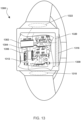
- FIG. 13 illustrates an example wearable computing device in the form of a smart watch 1300 according to some embodiments.
- a smart watch 1300 may include a processor 1302 coupled to internal memories 1304 and 1306.
- Internal memories 1304, 1306 may be volatile or non-volatile memories, and may also be secure and/or encrypted memories, or unsecure and/or unencrypted memories, or any combination thereof.
- the processor 1302 may also be coupled to a touchscreen display 1320, such as a resistive-sensing touchscreen, capacitive-sensing touchscreen infrared sensing touchscreen, or the like.
- the smart watch 1300 may have one or more antenna 1308 for sending and receiving electromagnetic radiation that may be connected to one or more wireless data links 1312, such as one or more Bluetooth ® transceivers, Peanut transceivers, Wi-Fi transceivers, ANT+ transceivers, etc., which may be coupled to the processor 1302.
- the smart watch 1300 may also include physical virtual buttons 1322 and 1310 for receiving user inputs as well as a slide sensor 1316 for receiving user inputs.
- the wireless data links 1312 and connected transceiver(s) may be used to electrically pair and communicate with external memory devices, such as a RAM/NVRAM coupled to a responding wireless transceiver.
- external memory devices such as a RAM/NVRAM coupled to a responding wireless transceiver.
- the smart watch 1300 may be temporarily paired with an external memory device (e.g., RAM 122), such that the processor (e.g., CPU 104) may configure the memory access control (e.g., access control hardware block 130) in preparation of issuing commands to access the memory (e.g., RAM cell array 138) of the memory device.
- the touchscreen display 1320 may be coupled to a touchscreen interface module that is configured receive signals from the touchscreen display 1320 indicative of locations on the screen where a user's fingertip or a stylus is touching the surface and output to the processor 1302 information regarding the coordinates of touch events. Further, the processor 1302 may be configured with processor-executable instructions to correlate images presented on the touchscreen display 1320 with the location of touch events received from the touchscreen interface module in order to detect when a user has interacted with a graphical interface icon, such as a virtual button.
- a graphical interface icon such as a virtual button
- the processor 1302 may be any programmable microprocessor, microcomputer or multiple processor chip or chips that can be configured by software instructions (applications) to perform a variety of functions, including the functions of the various embodiments. In some devices, multiple processors may be provided, such as one processor dedicated to wireless communication functions and one processor dedicated to running other applications. Typically, software applications may be stored in an internal memory before they are accessed and loaded into the processor 1302.
- the processor 1302 may include internal memory sufficient to store the application software instructions. In many devices the internal memory may be a volatile or nonvolatile memory, such as flash memory, or a mixture of both. For the purposes of this description, a general reference to memory refers to memory accessible by the processor 1302 including internal memory or removable memory plugged into the mobile device and memory within the processor 1302 itself.
- FIG. 14 is a component block diagram of an example of a network computing device 1400 that may provide secure in-memory device access of a memory device by a system-on-a-chip (SOC) according to some embodiments.
- a network computing device 1400 may function as a network element of a communication network, such as a base station.
- the network computing device 1400 may include a processor 1410 (e.g., CPU 104, NPU 308) coupled to volatile memory 1402 and a large capacity nonvolatile memory 1408 (e.g., RAM 122).
- the network computing device 1400 also may include a peripheral memory access device such as a floppy disc drive, compact disc (CD) or digital video disc (DVD) drive 1406 coupled to the processor 1410.
- the network computing device 1400 also may include network access ports 1404 (or interfaces) coupled to the processor 1410 for establishing data connections with a network, such as the Internet or a local area network coupled to other system computers and servers.
- the network computing device 1400 may include one or more antennas 1404 for sending and receiving electromagnetic radiation that may be connected to a wireless communication link.
- the network computing device 1400 may include additional access ports, such as USB, Firewire, Thunderbolt, and the like for coupling to peripherals, external memory, or other devices.
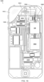
- FIG. 15 is a component block diagram of an example wireless device in the form of a smartphone 1500 suitable for implementing some embodiments.
- a smartphone 1500 may include a first SOC 140 (such as a SOC-CPU) coupled to a second SOC 1502 (such as a 5G capable SOC).
- the first and second SOCs 140, 1502 may be coupled to internal memory 1516 (e.g., SRAM 106), a display 1512, and to a speaker 1514.
- the smartphone 1500 may include an antenna 1504 for sending and receiving electromagnetic radiation that may be connected to a wireless data link or cellular telephone transceiver 1508 coupled to one or more processors in the first or second SOCs 140, 1502.
- the antenna 1504 may be used to electrically connect and issue configuration and mission mode memory access commands to an external memory device (e.g., RAM 122).
- Smartphones 1500 typically also include menu selection buttons or rocker switches 1520 for receiving user inputs.
- a typical smartphone 1500 also includes a sound encoding/decoding (CODEC) circuit 1510, which digitizes sound received from a microphone into data packets suitable for wireless transmission and decodes received sound data packets to generate analog signals that are provided to the speaker to generate sound.
- CODEC sound encoding/decoding
- one or more of the processors in the first and second SOCs 140, 1502, wireless transceiver 1508, and CODEC 1510 may include a digital signal processor (DSP) circuit (not shown separately).
- DSP digital signal processor
- the processors of the smart watch 1300, the wireless network computing device 1400, and the smart phone 1500 may be any programmable microprocessor, microcomputer or multiple processor chip or chips that may be configured by processor-executable instructions to perform a variety of functions, including the functions of the various embodiments described herein.
- multiple processors may be provided, such as one processor within the SOC 1502 dedicated to wireless communication functions and one processor within the SOC 140 dedicated to running other applications.
- software applications e.g., trusted programs 102, 306
- the processors may include internal memory sufficient to store the application software instructions.
- a component may be, but is not limited to, a process running on a processor, a processor, an object, an executable, a thread of execution, a program, or a computer.
- a component may be, but is not limited to, a process running on a processor, a processor, an object, an executable, a thread of execution, a program, or a computer.
- an application running on a wireless device and the wireless device may be referred to as a component.
- One or more components may reside within a process or thread of execution and a component may be localized on one processor or core or distributed between two or more processors or cores.
- these components may execute from various non-transitory computer readable media having various instructions or data structures stored thereon.
- Components may communicate by way of local or remote processes, function or procedure calls, electronic signals, data packets, memory read/writes, and other known network, computer, processor, or process related communication methodologies.
- the hardware and data processing apparatus used to implement the various illustrative logics, logical blocks, modules, and circuits described in connection with the aspects disclosed herein may be implemented or performed with a general purpose single- or multi-chip processor, a digital signal processor (DSP), an application specific integrated circuit (ASIC), a field programmable gate array (FPGA) or other programmable logic device, discrete gate or transistor logic, discrete hardware components, or any combination thereof designed to perform the functions described herein.
- a general-purpose processor may be a microprocessor, or any conventional processor, controller, microcontroller, or state machine.
- the functions described may be implemented in hardware, digital electronic circuitry, computer software, firmware, including the structures disclosed in this specification and their structural equivalents thereof, or in any combination thereof.
- Embodiments of the subject matter described in this specification also may be implemented as one or more computer programs, i.e. one or more modules of computer program instructions, encoded on a computer storage media for execution by, or to control the operation of, data processing apparatus.
- Computer program code or "program code” for execution on a programmable processor for carrying out operations of the various embodiments may be written in a high level programming language such as C, C++, C#, Smalltalk, Java, JavaScript, Visual Basic, a Structured Query Language (e.g., Transact-SQL), Perl, or in various other programming languages.
- Program code or programs stored on a computer readable storage medium as used in this application may refer to machine language code (such as object code) whose format is understandable by a processor.
- Computer-readable media includes both computer storage media and communication media including any medium that may be enabled to transfer a computer program from one place to another.
- a storage media may be any available media that may be accessed by a computer.
- such computer-readable media may include RAM, ROM, EEPROM, CD-ROM or other optical disk storage, magnetic disk storage or other magnetic storage devices, or any other medium that may be used to store desired program code in the form of instructions or data structures and that may be accessed by a computer.
- Disk and disc includes compact disc (CD), laser disc, optical disc, digital versatile disc (DVD), floppy disk, and Blu-ray disc in which disks usually reproduce data magnetically, while discs reproduce data optically with lasers. Combinations of the above should also be included within the scope of computer-readable media. Additionally, the operations of a method or algorithm may reside as one or any combination or set of codes and instructions on a machine readable medium and computer-readable medium, which may be incorporated into a computer program product.
Landscapes
- Engineering & Computer Science (AREA)
- Theoretical Computer Science (AREA)
- Computer Security & Cryptography (AREA)
- Physics & Mathematics (AREA)
- General Engineering & Computer Science (AREA)
- General Physics & Mathematics (AREA)
- Computer Hardware Design (AREA)
- Software Systems (AREA)
- Quality & Reliability (AREA)
- Storage Device Security (AREA)
Claims (14)
- Ein Verfahren (800, 1100) zum Angeben einer Zugriffsgewährung/-verweigerung-Rückmeldung zu einem System-on-Chip (SOC) als Teil einer Lese-/Schreibtransaktion-Sequenz einer Speichervorrichtung, aufweisend:Empfangen (1102) eines Entsperrkennworts von dem SOC,Bestimmen (1104), ob das empfangene Entsperrkennwort einem Kennwort in einem in der Speichervorrichtung gespeicherten Satz von annehmbaren Kennwörtern entspricht,Entsperren (1106) einer Speichervorrichtung-Gatterlogik, um zu erlauben, dass eine Speicherzugriffssteuerung eine Konfigurationsnachricht empfängt, in Antwort auf das Bestimmen, dass das empfangene Entsperrkennwort einem Kennwort in dem Satz von annehmbaren Kennwörtern entspricht,Empfangen (802) der Konfigurationsnachricht von dem SOC für das Konfigurieren der Speicherzugriffssteuerung der Speichervorrichtung,Konfigurieren (804) der Speicherzugriffssteuerung basierend auf der Konfigurationsnachricht,Empfangen (806) einer Zugriffsanfragenachricht von dem SOC, die einen Zugriff auf eine Speicherbasisadresse und einen Speicherzugriffsbereich eines Speicherzellenarrays der Speichervorrichtung anfragt, wobei die Zugriffsanfragenachricht eine Lese-/Schreiboperation umfasst,Vergleichen (808) der Zugriffsanfragenachricht mit der konfigurierten Speicherzugriffssteuerung, um zu bestimmen, ob die Zugriffsanfragenachricht zulässig ist, undDurchführen (810) der Lese-/Schreiboperation in Antwort auf das Bestimmen, dass die Zugriffsanfragenachricht zulässig ist.
- Verfahren (800, 1100) nach Anspruch 1, wobei:die Konfigurationsnachricht eine Konfigurationssicherheitsdomänen-ID enthält, unddie Zugriffsanfragenachricht eine angefragte Sicherheitsdomänen-ID enthält.
- Verfahren nach Anspruch 2, wobei das Vergleichen der Zugriffsanfragenachricht mit der konfigurierten Speicherzugriffssteuerung, um zu bestimmen, ob die Zugriffsanfragenachricht zulässig ist, aufweist:Bestimmen (902), ob die Konfigurationssicherheitsdomänen-ID der angefragten Sicherheitsdomänen-ID entspricht, undin Antwort auf das Bestimmen, dass die Konfigurationssicherheitsdomänen-ID der angefragten Sicherheitsdomänen-ID entspricht:Bestimmen (904), dass die Zugriffsanfragenachricht zulässig ist, undSenden einer Benachrichtigung an den SOC, die angibt, dass die Zugriffsanfragenachricht zulässig ist.
- Verfahren nach Anspruch 3, das weiterhin aufweist:in Antwort auf das Bestimmen, dass die Konfigurationssicherheitsdomänen-ID nicht der angefragten Sicherheitsdomänen-ID entspricht,Bestimmen (1002), dass die Zugriffsanfragenachricht unzulässig ist,Speichern (1004) von Fehlerinformationen einschließlich der Speicherbasisadresse, des Speicherzugriffsbereichs und der angefragten Sicherheitsdomänen-ID,Senden einer Benachrichtigung an den SOC, die angibt, dass die Zugriffsanfragenachricht unzulässig ist, undSenden (1006) der Fehlerinformationen an den SOC in Antwort auf das Empfangen einer Unterbrechungsanfrage von dem SOC.
- Verfahren nach Anspruch 2, wobei:die Konfigurationsnachricht eine codierte JEDEC-Nachricht ist, die die Konfigurationssicherheitsdomänen-ID enthält, unddie Zugriffsanfragenachricht eine codierte JEDEC-Nachricht ist, die die angefragte Sicherheitsdomänen-ID enthält.
- Verfahren nach Anspruch 1, das weiterhin aufweist:Empfangen (1202), von dem SOC, eines Sperrbefehls, der konfiguriert ist zum Setzen eines Sperrbits in einem Register der Speichervorrichtung, undSetzen (1204) des Sperrbits, um Konfigurationsänderungen an der konfigurierten Speicherzugriffssteuerung zu verhindern.
- Eine Speichervorrichtung (122), aufweisend:ein Speicherzellenarray (138),eine Speichervorrichtung-Gatterlogik (126),einen Vertrauen-Hardwareblock (125), wobei der Vertrauen-Hardwareblock (125) konfiguriert ist zum Durchführen von Operationen, die weiterhin aufweisen:Empfangen eines Entsperrkennworts von einem System-on-Chip (SOC),Bestimmen, ob das empfangene Entsperrkennwort einem Kennwort in einem in der Speichervorrichtung (122) gespeicherten Satz von annehmbaren Kennwörtern entspricht, undEntsperren der Speichervorrichtung-Gatterlogik (126), um zu erlauben, dass ein Zugriffssteuerung-Hardwareblock (130) eine Konfigurationsnachricht empfängt, in Antwort auf das Bestimmen, dass das empfangene Entsperrkennwort einem Kennwort in dem Satz von annehmbaren Kennwörtern entspricht,wobei der Zugriffssteuerung-Hardwarblock (130) konfiguriert ist zum durchführen von Operationen, die aufweisen:Empfangen der Konfigurationsnachricht von dem SOC für das Konfigurieren der Speicherzugriffssteuerung der Speichervorrichtung (122),Konfigurieren einer Speicherzugriffssteuerung basierend auf der Konfigurationsnachricht,Empfangen einer Zugriffsanfragenachricht von dem SOC, die einen Zugriff auf eine Speicherbasisadresse und einen Speicherzugriffsbereich des Speicherzellenarrays (138) anfragt, wobei die Zugriffsanfragenachricht eine Lese-/Schreiboperation umfasst,Vergleichen der Zugriffsanfragenachricht mit der konfigurierten Speicherzugriffssteuerung, um zu bestimmen, ob die Zugriffsanfragenachricht zulässig ist, undDurchführen der Lese-/Schreiboperation in Antwort auf das Bestimmen, dass die Zugriffsanfragenachricht zulässig ist.
- Speichervorrichtung (122) nach Anspruch 7, wobei der Zugriffssteuerung-Hardwareblock (130) konfiguriert ist zum Durchführen von Operationen derart, dass:das Empfangen der Konfigurationsnachricht von dem SOC das Empfangen einer Konfigurationsnachricht, die eine Konfigurationssicherheitsdomänen-ID enthält, aufweist, unddas Empfangen einer Zugriffsanfragenachricht von dem SOC das Empfangen einer Zugriffsanfragenachricht, die eine angefragte Sicherheitsdomänen-ID enthält, aufweist.
- Speichervorrichtung (122) nach Anspruch 8, wobei der Zugriffssteuerung-Hardwareblock (130) konfiguriert ist zum Durchführen von Operationen derart, dass das Vergleichen der Zugriffsanfragenachricht mit der konfigurierten Speicherzugriffssteuerung, um zu bestimmen, ob die Zugriffsanfragenachricht zulässig ist, aufweist:Bestimmen, ob die Konfigurationssicherheitsdomänen-ID der angefragten Sicherheitsdomänen-ID entspricht, undin Antwort auf das Bestimmen, dass die Konfigurationssicherheitsdomänen-ID der angefragten Sicherheitsdomänen-ID entspricht,Bestimmen, dass die Zugriffsanfragenachricht zulässig ist, undSenden einer Benachrichtigung an den SOC, die angibt, dass die Zugriffsanfragenachricht zulässig ist.
- Speichervorrichtung (122) nach Anspruch 9, wobei der Zugriffssteuerung-Hardwareblock (130) konfiguriert ist zum Durchführen von Operationen, die weiterhin aufweisen:
in Antwort auf das Bestimmen, dass die Konfigurationssicherheitsdomänen-ID nicht der angefragten Sicherheitsdomänen-ID entspricht:Bestimmen, dass die Zugriffsanfragenachricht unzulässig ist,Speichern von Fehlerinformationen einschließlich der Speicherbasisadresse, des Speicherzugriffsbereichs und der angefragten Sicherheitsdomänen-ID,Senden einer Benachrichtigung an den SOC, die angibt, dass die Zugriffsanfragenachricht unzulässig ist, undSenden der Fehlerinformationen an den SOC in Antwort auf das Empfangen einer Fehlerunterbrechungsanfrage von dem SOC. - Speichervorrichtung (122) nach Anspruch 8, wobei der Zugriffssteuerung-Hardwareblock (130) konfiguriert ist zum Durchführen von Operationen derart, dass:das Empfangen der Konfigurationsnachricht von dem SOC das Empfangen einer codierten JEDEC-Nachricht, die die Konfigurationssicherheitsdomänen-ID enthält, aufweist, unddas Empfangen einer Zugriffsanfragenachricht von dem SOC das Empfangen einer codierten JEDEC-Nachricht, die die angefragte Sicherheitsdomänen-ID enthält, aufweist.
- Speichervorrichtung (122) nach Anspruch 7, wobei der Zugriffssteuerung-Hardwareblock (130) konfiguriert ist zum Durchführen von Operationen, die weiterhin aufweisen:Empfangen, von dem SOC, eines Sperrbefehls, der konfiguriert ist zum Setzen eines Sperrbits in einem Register der Speichervorrichtung, undSetzen des Sperrbits, um Konfigurationsänderungen an der konfigurierten Speicherzugriffssteuerung zu verhindern.
- Speichervorrichtung (122) nach Anspruch 7, wobei der Vertrauen-Hardwareblock (125) aufweist:einen Sicherungsspeicher (128), der konfiguriert ist zum Speichern eines Satzes von annehmbaren Kennwörtern,ein Gewährungsgatter (202), das die Speichervorrichtung-Gatterlogik aufweist undeinen Logikblock (204), der mit dem Sicherungsspeicher (128) und dem Gewährungsgatter (202) gekoppelt ist und konfiguriert ist zum:Bestimmen, ob das empfangene Entsperrkennwort dem Kennwort in dem in dem Sicherungsspeicher gespeicherten Satz von annehmbaren Kennwörtern entspricht, undSignalisieren, dass das Gewährungsgatter die Speichervorrichtung-Gatterlogik entsperren soll, in Antwort auf das Bestimmen, dass das empfangene Entsperrkennwort dem Kennwort in dem in dem Sicherheitsspeicher gespeicherten Satz von annehmbaren Kennwörtern entspricht.
- Speichervorrichtung (122) nach Anspruch 7, wobei der Zugriffssteuerung-Hardwareblock (130) aufweist:einen Zugriffssteuerung-Konfigurationsblock (132),ein Zugriffsverweigerungssyndrom (134), undeinen Richtlinienerzwingungsblock (136).
Applications Claiming Priority (2)
| Application Number | Priority Date | Filing Date | Title |
|---|---|---|---|
| US16/937,907 US11636231B2 (en) | 2020-07-24 | 2020-07-24 | Methods and apparatus for in-memory device access control |
| PCT/US2021/042148 WO2022020225A1 (en) | 2020-07-24 | 2021-07-19 | Methods and apparatus for in-memory device access control |
Publications (3)
| Publication Number | Publication Date |
|---|---|
| EP4185980A1 EP4185980A1 (de) | 2023-05-31 |
| EP4185980C0 EP4185980C0 (de) | 2024-07-10 |
| EP4185980B1 true EP4185980B1 (de) | 2024-07-10 |
Family
ID=77301004
Family Applications (1)
| Application Number | Title | Priority Date | Filing Date |
|---|---|---|---|
| EP21752815.7A Active EP4185980B1 (de) | 2020-07-24 | 2021-07-19 | Verfahren und vorrichtung zur speicherinternen gerätezugriffssteuerung |
Country Status (6)
| Country | Link |
|---|---|
| US (1) | US11636231B2 (de) |
| EP (1) | EP4185980B1 (de) |
| KR (1) | KR102837857B1 (de) |
| CN (1) | CN116157797A (de) |
| TW (1) | TWI879999B (de) |
| WO (1) | WO2022020225A1 (de) |
Families Citing this family (15)
| Publication number | Priority date | Publication date | Assignee | Title |
|---|---|---|---|---|
| US20220035956A1 (en) * | 2020-07-30 | 2022-02-03 | Hewlett Packard Enterprise Development Lp | Password-based access control for programmable logic devices |
| CN115918116A (zh) * | 2020-10-09 | 2023-04-04 | Oppo广东移动通信有限公司 | 信息处理方法、装置及存储介质 |
| GB2605774B (en) * | 2021-04-07 | 2023-04-19 | Advanced Risc Mach Ltd | Apparatus and method for handling stashing transactions |
| US12067261B2 (en) * | 2021-07-15 | 2024-08-20 | Rambus Inc. | Serial presence detect logging |
| US12287910B2 (en) * | 2021-09-09 | 2025-04-29 | Toyota Motor North America, Inc. | Transport limitation for data reads |
| FR3129499B1 (fr) * | 2021-11-25 | 2024-06-28 | Stmicroelectronics Grand Ouest Sas | Gestion dynamique d’un pare-feu de mémoire |
| CN117556412A (zh) * | 2022-08-03 | 2024-02-13 | 阿里巴巴(中国)有限公司 | 用于内存的处理单元及其存取检测方法 |
| US12432204B2 (en) * | 2022-09-23 | 2025-09-30 | Qualcomm Incorporated | Hardware identity impersonation for target access control |
| US12353272B2 (en) * | 2022-09-23 | 2025-07-08 | Apple Inc. | Error logger circuit |
| KR20240092317A (ko) * | 2022-12-14 | 2024-06-24 | 삼성전자주식회사 | 메모리 장치, 메모리 장치의 동작 방법 및 메모리 시스템 |
| CN117472808A (zh) * | 2023-08-21 | 2024-01-30 | 华为技术有限公司 | 数据保护方法、装置及系统 |
| US20250139307A1 (en) * | 2023-10-26 | 2025-05-01 | Nokia Solutions And Networks Oy | Router including anti-theft features |
| US20240320347A1 (en) * | 2024-05-30 | 2024-09-26 | Intel Corporation | Host-memory certificate exchange for secure access to memory storage and register space |
| CN118519959B (zh) * | 2024-07-24 | 2024-11-12 | 山东航天电子技术研究所 | 一种多用途通用性数据处理与控制SiP微系统 |
| CN119312353A (zh) * | 2024-12-13 | 2025-01-14 | 湖北芯擎科技有限公司 | 端侧模型调用系统、方法及计算机可读存储介质 |
Family Cites Families (9)
| Publication number | Priority date | Publication date | Assignee | Title |
|---|---|---|---|---|
| US9612977B2 (en) * | 2011-07-15 | 2017-04-04 | Standard Microsystems Corporation | Method and system for controlling access to embedded nonvolatile memories |
| US8893267B1 (en) * | 2011-08-17 | 2014-11-18 | Applied Micro Circuits Corporation | System and method for partitioning resources in a system-on-chip (SoC) |
| US8775757B2 (en) * | 2012-09-25 | 2014-07-08 | Apple Inc. | Trust zone support in system on a chip having security enclave processor |
| US20140310536A1 (en) * | 2013-04-16 | 2014-10-16 | Qualcomm Incorporated | Storage device assisted inline encryption and decryption |
| CN105468962A (zh) * | 2014-09-03 | 2016-04-06 | 阿里巴巴集团控股有限公司 | 用户界面解锁的方法及装置 |
| US20180121125A1 (en) * | 2016-11-01 | 2018-05-03 | Qualcomm Incorporated | Method and apparatus for managing resource access control hardware in a system-on-chip device |
| US10387333B2 (en) * | 2017-01-05 | 2019-08-20 | Qualcomm Incorporated | Non-volatile random access memory with gated security access |
| US10591975B2 (en) * | 2017-10-30 | 2020-03-17 | Qualcomm Incorporated | Memory access management for low-power use cases of a system on chip via secure non-volatile random access memory |
| US11431494B2 (en) * | 2018-03-15 | 2022-08-30 | Atakama LLC | Passwordless security system for data-at-rest |
-
2020
- 2020-07-24 US US16/937,907 patent/US11636231B2/en active Active
-
2021
- 2021-07-19 EP EP21752815.7A patent/EP4185980B1/de active Active
- 2021-07-19 TW TW110126422A patent/TWI879999B/zh active
- 2021-07-19 KR KR1020237001834A patent/KR102837857B1/ko active Active
- 2021-07-19 CN CN202180061498.0A patent/CN116157797A/zh active Pending
- 2021-07-19 WO PCT/US2021/042148 patent/WO2022020225A1/en not_active Ceased
Also Published As
| Publication number | Publication date |
|---|---|
| US20220027520A1 (en) | 2022-01-27 |
| EP4185980A1 (de) | 2023-05-31 |
| EP4185980C0 (de) | 2024-07-10 |
| KR102837857B1 (ko) | 2025-07-23 |
| BR112023000518A2 (pt) | 2023-01-31 |
| WO2022020225A1 (en) | 2022-01-27 |
| TW202221498A (zh) | 2022-06-01 |
| KR20230042455A (ko) | 2023-03-28 |
| CN116157797A (zh) | 2023-05-23 |
| US11636231B2 (en) | 2023-04-25 |
| TWI879999B (zh) | 2025-04-11 |
Similar Documents
| Publication | Publication Date | Title |
|---|---|---|
| EP4185980B1 (de) | Verfahren und vorrichtung zur speicherinternen gerätezugriffssteuerung | |
| CN100465924C (zh) | 存储装置 | |
| EP3274850B1 (de) | Schutz eines speichers | |
| US9256734B2 (en) | Security controlled multi-processor system | |
| US10318765B2 (en) | Protecting critical data structures in an embedded hypervisor system | |
| TWI402682B (zh) | 對嵌入式控制器的記憶體保護 | |
| JP7213879B2 (ja) | 間接アクセスメモリコントローラ用のメモリ保護装置 | |
| US12147588B2 (en) | Controlled access to data stored in a secure partition | |
| US11615207B2 (en) | Security processor configured to authenticate user and authorize user for user data and computing system including the same | |
| US20140089650A1 (en) | Security Enclave Processor Boot Control | |
| KR101870847B1 (ko) | 단말 디바이스의 디버그 포트 제어 방법 및 장치 | |
| US10897359B2 (en) | Controlled storage device access | |
| WO2020029254A1 (zh) | 一种SoC芯片及总线访问控制方法 | |
| EP1801700B1 (de) | System und Verfahren zur Verwendungsbegrenzung eines DMA Kanals | |
| WO2022126644A1 (zh) | 模型保护装置及方法、计算装置 | |
| CN112016090B (zh) | 安全计算卡,基于安全计算卡的度量方法及系统 | |
| CN110276214A (zh) | 一种基于从机访问保护的双核可信soc架构及方法 | |
| WO2025128420A1 (en) | Techniques for enforcing access control policies for application-specific integrated circuits (asics) | |
| CN102473225B (zh) | 用于保护数字存储设备的方法、系统和设备 | |
| BR112023000518B1 (pt) | Método para indicar passagem de acesso/realimentação de violação a um sistema em chip, soc, como parte de uma sequência de transação de leitura/gravação de um dispositivo de memória e dispositivo de memória | |
| US11182509B2 (en) | Hardware-based system for cybersecurity protection of microprocessor systems | |
| CN111736770A (zh) | 嵌入式安全存储器 | |
| CN108270910A (zh) | 移动终端 | |
| CN120372634A (zh) | 针对管理控制器的加密密钥 | |
| HK40039143A (en) | Security computing card, and measurement method and system based on secruity computing card |
Legal Events
| Date | Code | Title | Description |
|---|---|---|---|
| STAA | Information on the status of an ep patent application or granted ep patent |
Free format text: STATUS: UNKNOWN |
|
| STAA | Information on the status of an ep patent application or granted ep patent |
Free format text: STATUS: THE INTERNATIONAL PUBLICATION HAS BEEN MADE |
|
| PUAI | Public reference made under article 153(3) epc to a published international application that has entered the european phase |
Free format text: ORIGINAL CODE: 0009012 |
|
| STAA | Information on the status of an ep patent application or granted ep patent |
Free format text: STATUS: REQUEST FOR EXAMINATION WAS MADE |
|
| 17P | Request for examination filed |
Effective date: 20221201 |
|
| AK | Designated contracting states |
Kind code of ref document: A1 Designated state(s): AL AT BE BG CH CY CZ DE DK EE ES FI FR GB GR HR HU IE IS IT LI LT LU LV MC MK MT NL NO PL PT RO RS SE SI SK SM TR |
|
| DAV | Request for validation of the european patent (deleted) | ||
| DAX | Request for extension of the european patent (deleted) | ||
| GRAP | Despatch of communication of intention to grant a patent |
Free format text: ORIGINAL CODE: EPIDOSNIGR1 |
|
| STAA | Information on the status of an ep patent application or granted ep patent |
Free format text: STATUS: GRANT OF PATENT IS INTENDED |
|
| INTG | Intention to grant announced |
Effective date: 20231123 |
|
| GRAJ | Information related to disapproval of communication of intention to grant by the applicant or resumption of examination proceedings by the epo deleted |
Free format text: ORIGINAL CODE: EPIDOSDIGR1 |
|
| STAA | Information on the status of an ep patent application or granted ep patent |
Free format text: STATUS: REQUEST FOR EXAMINATION WAS MADE |
|
| GRAP | Despatch of communication of intention to grant a patent |
Free format text: ORIGINAL CODE: EPIDOSNIGR1 |
|
| STAA | Information on the status of an ep patent application or granted ep patent |
Free format text: STATUS: GRANT OF PATENT IS INTENDED |
|
| INTC | Intention to grant announced (deleted) | ||
| INTG | Intention to grant announced |
Effective date: 20240326 |
|
| GRAS | Grant fee paid |
Free format text: ORIGINAL CODE: EPIDOSNIGR3 |
|
| GRAA | (expected) grant |
Free format text: ORIGINAL CODE: 0009210 |
|
| STAA | Information on the status of an ep patent application or granted ep patent |
Free format text: STATUS: THE PATENT HAS BEEN GRANTED |
|
| AK | Designated contracting states |
Kind code of ref document: B1 Designated state(s): AL AT BE BG CH CY CZ DE DK EE ES FI FR GB GR HR HU IE IS IT LI LT LU LV MC MK MT NL NO PL PT RO RS SE SI SK SM TR |
|
| REG | Reference to a national code |
Ref country code: CH Ref legal event code: EP |
|
| REG | Reference to a national code |
Ref country code: DE Ref legal event code: R096 Ref document number: 602021015553 Country of ref document: DE |
|
| U01 | Request for unitary effect filed |
Effective date: 20240722 |
|
| U07 | Unitary effect registered |
Designated state(s): AT BE BG DE DK EE FI FR IT LT LU LV MT NL PT RO SE SI Effective date: 20240902 |
|
| U20 | Renewal fee for the european patent with unitary effect paid |
Year of fee payment: 4 Effective date: 20241126 |
|
| PG25 | Lapsed in a contracting state [announced via postgrant information from national office to epo] |
Ref country code: NO Free format text: LAPSE BECAUSE OF FAILURE TO SUBMIT A TRANSLATION OF THE DESCRIPTION OR TO PAY THE FEE WITHIN THE PRESCRIBED TIME-LIMIT Effective date: 20241010 |
|
| PG25 | Lapsed in a contracting state [announced via postgrant information from national office to epo] |
Ref country code: GR Free format text: LAPSE BECAUSE OF FAILURE TO SUBMIT A TRANSLATION OF THE DESCRIPTION OR TO PAY THE FEE WITHIN THE PRESCRIBED TIME-LIMIT Effective date: 20241011 Ref country code: PL Free format text: LAPSE BECAUSE OF FAILURE TO SUBMIT A TRANSLATION OF THE DESCRIPTION OR TO PAY THE FEE WITHIN THE PRESCRIBED TIME-LIMIT Effective date: 20240710 |
|
| PG25 | Lapsed in a contracting state [announced via postgrant information from national office to epo] |
Ref country code: IS Free format text: LAPSE BECAUSE OF FAILURE TO SUBMIT A TRANSLATION OF THE DESCRIPTION OR TO PAY THE FEE WITHIN THE PRESCRIBED TIME-LIMIT Effective date: 20241110 |
|
| PG25 | Lapsed in a contracting state [announced via postgrant information from national office to epo] |
Ref country code: HR Free format text: LAPSE BECAUSE OF FAILURE TO SUBMIT A TRANSLATION OF THE DESCRIPTION OR TO PAY THE FEE WITHIN THE PRESCRIBED TIME-LIMIT Effective date: 20240710 |
|
| PG25 | Lapsed in a contracting state [announced via postgrant information from national office to epo] |
Ref country code: ES Free format text: LAPSE BECAUSE OF FAILURE TO SUBMIT A TRANSLATION OF THE DESCRIPTION OR TO PAY THE FEE WITHIN THE PRESCRIBED TIME-LIMIT Effective date: 20240710 Ref country code: RS Free format text: LAPSE BECAUSE OF FAILURE TO SUBMIT A TRANSLATION OF THE DESCRIPTION OR TO PAY THE FEE WITHIN THE PRESCRIBED TIME-LIMIT Effective date: 20241010 |
|
| PG25 | Lapsed in a contracting state [announced via postgrant information from national office to epo] |
Ref country code: RS Free format text: LAPSE BECAUSE OF FAILURE TO SUBMIT A TRANSLATION OF THE DESCRIPTION OR TO PAY THE FEE WITHIN THE PRESCRIBED TIME-LIMIT Effective date: 20241010 Ref country code: PL Free format text: LAPSE BECAUSE OF FAILURE TO SUBMIT A TRANSLATION OF THE DESCRIPTION OR TO PAY THE FEE WITHIN THE PRESCRIBED TIME-LIMIT Effective date: 20240710 Ref country code: NO Free format text: LAPSE BECAUSE OF FAILURE TO SUBMIT A TRANSLATION OF THE DESCRIPTION OR TO PAY THE FEE WITHIN THE PRESCRIBED TIME-LIMIT Effective date: 20241010 Ref country code: IS Free format text: LAPSE BECAUSE OF FAILURE TO SUBMIT A TRANSLATION OF THE DESCRIPTION OR TO PAY THE FEE WITHIN THE PRESCRIBED TIME-LIMIT Effective date: 20241110 Ref country code: HR Free format text: LAPSE BECAUSE OF FAILURE TO SUBMIT A TRANSLATION OF THE DESCRIPTION OR TO PAY THE FEE WITHIN THE PRESCRIBED TIME-LIMIT Effective date: 20240710 Ref country code: GR Free format text: LAPSE BECAUSE OF FAILURE TO SUBMIT A TRANSLATION OF THE DESCRIPTION OR TO PAY THE FEE WITHIN THE PRESCRIBED TIME-LIMIT Effective date: 20241011 Ref country code: ES Free format text: LAPSE BECAUSE OF FAILURE TO SUBMIT A TRANSLATION OF THE DESCRIPTION OR TO PAY THE FEE WITHIN THE PRESCRIBED TIME-LIMIT Effective date: 20240710 |
|
| REG | Reference to a national code |
Ref country code: CH Ref legal event code: PL |
|
| PG25 | Lapsed in a contracting state [announced via postgrant information from national office to epo] |
Ref country code: SM Free format text: LAPSE BECAUSE OF FAILURE TO SUBMIT A TRANSLATION OF THE DESCRIPTION OR TO PAY THE FEE WITHIN THE PRESCRIBED TIME-LIMIT Effective date: 20240710 |
|
| PG25 | Lapsed in a contracting state [announced via postgrant information from national office to epo] |
Ref country code: MC Free format text: LAPSE BECAUSE OF FAILURE TO SUBMIT A TRANSLATION OF THE DESCRIPTION OR TO PAY THE FEE WITHIN THE PRESCRIBED TIME-LIMIT Effective date: 20240710 Ref country code: CH Free format text: LAPSE BECAUSE OF NON-PAYMENT OF DUE FEES Effective date: 20240731 |
|
| PG25 | Lapsed in a contracting state [announced via postgrant information from national office to epo] |
Ref country code: CZ Free format text: LAPSE BECAUSE OF FAILURE TO SUBMIT A TRANSLATION OF THE DESCRIPTION OR TO PAY THE FEE WITHIN THE PRESCRIBED TIME-LIMIT Effective date: 20240710 |
|
| PG25 | Lapsed in a contracting state [announced via postgrant information from national office to epo] |
Ref country code: SK Free format text: LAPSE BECAUSE OF FAILURE TO SUBMIT A TRANSLATION OF THE DESCRIPTION OR TO PAY THE FEE WITHIN THE PRESCRIBED TIME-LIMIT Effective date: 20240710 |
|
| PLBE | No opposition filed within time limit |
Free format text: ORIGINAL CODE: 0009261 |
|
| STAA | Information on the status of an ep patent application or granted ep patent |
Free format text: STATUS: NO OPPOSITION FILED WITHIN TIME LIMIT |
|
| 26N | No opposition filed |
Effective date: 20250411 |
|
| PGFP | Annual fee paid to national office [announced via postgrant information from national office to epo] |
Ref country code: GB Payment date: 20250612 Year of fee payment: 5 |
|
| U20 | Renewal fee for the european patent with unitary effect paid |
Year of fee payment: 5 Effective date: 20250617 |
|
| PGFP | Annual fee paid to national office [announced via postgrant information from national office to epo] |
Ref country code: IE Payment date: 20250612 Year of fee payment: 5 |
|
| PG25 | Lapsed in a contracting state [announced via postgrant information from national office to epo] |
Ref country code: CY Free format text: LAPSE BECAUSE OF FAILURE TO SUBMIT A TRANSLATION OF THE DESCRIPTION OR TO PAY THE FEE WITHIN THE PRESCRIBED TIME-LIMIT; INVALID AB INITIO Effective date: 20210719 |
|
| PG25 | Lapsed in a contracting state [announced via postgrant information from national office to epo] |
Ref country code: HU Free format text: LAPSE BECAUSE OF FAILURE TO SUBMIT A TRANSLATION OF THE DESCRIPTION OR TO PAY THE FEE WITHIN THE PRESCRIBED TIME-LIMIT; INVALID AB INITIO Effective date: 20210719 |