EP4185877B1 - Current transducer - Google Patents
Current transducer Download PDFInfo
- Publication number
- EP4185877B1 EP4185877B1 EP21740559.6A EP21740559A EP4185877B1 EP 4185877 B1 EP4185877 B1 EP 4185877B1 EP 21740559 A EP21740559 A EP 21740559A EP 4185877 B1 EP4185877 B1 EP 4185877B1
- Authority
- EP
- European Patent Office
- Prior art keywords
- chip
- primary conductor
- current transducer
- connection terminals
- thickness
- Prior art date
- Legal status (The legal status is an assumption and is not a legal conclusion. Google has not performed a legal analysis and makes no representation as to the accuracy of the status listed.)
- Active
Links
Images


Classifications
-
- G—PHYSICS
- G01—MEASURING; TESTING
- G01R—MEASURING ELECTRIC VARIABLES; MEASURING MAGNETIC VARIABLES
- G01R15/00—Details of measuring arrangements of the types provided for in groups G01R17/00 - G01R29/00, G01R33/00 - G01R33/26 or G01R35/00
- G01R15/14—Adaptations providing voltage or current isolation, e.g. for high-voltage or high-current networks
- G01R15/20—Adaptations providing voltage or current isolation, e.g. for high-voltage or high-current networks using galvano-magnetic devices, e.g. Hall-effect devices, i.e. measuring a magnetic field via the interaction between a current and a magnetic field, e.g. magneto resistive or Hall effect devices
- G01R15/202—Adaptations providing voltage or current isolation, e.g. for high-voltage or high-current networks using galvano-magnetic devices, e.g. Hall-effect devices, i.e. measuring a magnetic field via the interaction between a current and a magnetic field, e.g. magneto resistive or Hall effect devices using Hall-effect devices
-
- G—PHYSICS
- G01—MEASURING; TESTING
- G01R—MEASURING ELECTRIC VARIABLES; MEASURING MAGNETIC VARIABLES
- G01R15/00—Details of measuring arrangements of the types provided for in groups G01R17/00 - G01R29/00, G01R33/00 - G01R33/26 or G01R35/00
- G01R15/14—Adaptations providing voltage or current isolation, e.g. for high-voltage or high-current networks
- G01R15/20—Adaptations providing voltage or current isolation, e.g. for high-voltage or high-current networks using galvano-magnetic devices, e.g. Hall-effect devices, i.e. measuring a magnetic field via the interaction between a current and a magnetic field, e.g. magneto resistive or Hall effect devices
- G01R15/205—Adaptations providing voltage or current isolation, e.g. for high-voltage or high-current networks using galvano-magnetic devices, e.g. Hall-effect devices, i.e. measuring a magnetic field via the interaction between a current and a magnetic field, e.g. magneto resistive or Hall effect devices using magneto-resistance devices, e.g. field plates
-
- G—PHYSICS
- G01—MEASURING; TESTING
- G01R—MEASURING ELECTRIC VARIABLES; MEASURING MAGNETIC VARIABLES
- G01R15/00—Details of measuring arrangements of the types provided for in groups G01R17/00 - G01R29/00, G01R33/00 - G01R33/26 or G01R35/00
- G01R15/14—Adaptations providing voltage or current isolation, e.g. for high-voltage or high-current networks
- G01R15/20—Adaptations providing voltage or current isolation, e.g. for high-voltage or high-current networks using galvano-magnetic devices, e.g. Hall-effect devices, i.e. measuring a magnetic field via the interaction between a current and a magnetic field, e.g. magneto resistive or Hall effect devices
- G01R15/207—Constructional details independent of the type of device used
Definitions
- the present invention relates to an open-loop current transducer for surface mounting on a circuit board.
- Such coreless current transducers may include an integrated circuit (IC) chip having an active sensing layer thereon detecting the magnetic field induced by a current to be measured flowing in a primary conductor integrated within the current transducer, the integrated circuit chip being electrically connected to secondary contacts that supply power and allow transmission of the measurement signal to the external circuit board.
- IC integrated circuit
- a lead frame is a strip of sheet metal that is stamped and formed to cut out primary and secondary contacts from the sheet metal, the contacts and integrated circuit being overmolded by an insulating polymer, connection ends of the contacts being exposed and configured for a solder or welding connection to circuit traces on the circuit board.
- the electrical interconnection between the integrated circuit and the secondary contacts may be connected by a so-called "flip-chip” connection or by wire bonding.
- Active portions and connection interfaces on the semi-conductor substrate which, for instance a CMOS IC, are typically provided on a same single side of the IC.
- a flip-chip arrangement for instance as described in US 2006/219436 A1 , allows the active side to be facing and adjacent the lead frame conductor arrangement, allowing electrical interconnection between the lead frame and connection portions on the integrated circuit active surface, while at the same time having the active sensing portion of the integrated circuit being very close to the primary conductor. This provides greater sensitivity for measurement of the primary current due to the very small distance between the sensing layer and the primary conductor.
- Flip-chip connections can however be costly and complex to manufacture because of the small distances on the IC chip between connection points that need to be directly connected to the secondary conductors of the lead frame arrangement. There may also be disadvantages regarding electrical creepage distances that are more difficult to manage than in wire bond interconnections.
- Wire bonding is a very common and widely used technique for interconnecting integrated circuits to conductors forming connection terminals for the IC chip.
- a drawback of wire bonding interconnections between the IC chip and the lead frame arrangement is however the increased height compared to flip-chip arrangements due to the height of the interconnecting wire loops between the IC substrate and the lead frame conductors.
- the active sensor side faces away from the lead frame conductor arrangement in order to have the active surface accessible for the wire bonding between the lead frame terminals and the connection points on the IC circuit. There is thus a lower sensitivity compared to a flip-chip arrangement.
- an object of the present invention is to overcome the drawbacks of both conventional flip-chip and conventional wire bonded arrangements in open-loop current transducers for surface mount on circuit boards.
- an open-loop electrical current transducer for surface mounting on an external circuit board, comprising an integrated circuit (IC) chip comprising
- the lead frame arrangement is formed from sheet metal having a base sheet of thickness B wherein at least portions of the lead frame arrangement comprise a thickness equal to said base sheet thickness B.
- the first active side of the IC chip faces the lead frame arrangement and at least a portion of the lead frame arrangement comprises a thinned portion of thickness T between 20% and 80% of the base sheet thickness B, said thinned portion of thickness T including said IC connection portions of the secondary conductors .
- the IC chip is mounted partially overlapping a portion of the primary conductor including a sensing portion of the primary conductor, an insulating sheet mounted between the IC chip and primary conductor made of a material different from a material forming the insulating overmold housing, the connection terminals of the IC chip being provided on said portion of the IC chip not overlapping the primary conductor.
- said insulating foil extends beyond the portion of IC chip overlapping the primary conductor with a border of non-zero width W for increasing an electrical creepage distance between the primary conductor and IC chip.
- said insulating foil extends beyond an edge of the primary conductor over which the IC chip also extends in order to increase the creepage distance between the IC chip and the primary conductor.
- the sensing portion has a reduced current carrying cross-sectional area compared to surface mount connection terminals of the primary conductor between which the sensing portion is positioned and interconnected.
- surface mount connection terminals of the secondary conductors are arranged in a row along a first edge of the overmold housing and the surface mount connection terminals of the primary conductor are arranged adjacent an opposed edge of the overmold housing.
- the thinned portion thickness T is in the range of 30% to 70% of base sheet thickness B.
- the thinned portion thickness T is in the range of 40% to 60% of base sheet thickness B.
- the primary conductor comprises one or more heat sink extensions serving as heat sinks extending from the surface mount connection terminals thereof.
- the one or more heat sink extensions extend from the primary conductor surface mount connection terminals towards the surface mount connection terminals of the secondary conductors.
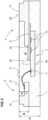
- an electric current transducer 1 for surface mount connection on an external circuit board comprises a magnetic field sensor 2 connected to a lead frame arrangement 3 housed within an insulating overmold housing 7.
- the magnetic field sensor 2 is in the form of an integrated circuit (IC) chip having a first active side 9a and a second side 9b, at least the first active side 9a having active portions including electrical connection terminals 11 for connection to power and signal transmission conductors and a magnetic field sensor portion 10 arranged at or close to the surface of the first side.
- the chip may be attached to the lead frame with a glue layer between the face 9a and the insulating layer 8.
- the insulating layer 8 may be attached to the lead frame with a glue layer.
- the magnetic field sensing portion 10 may comprise a Hall effect sensor, or a giant magnetoresistive sensor or other forms of magnetic field sensors that are per se well known in the art.
- the IC chip 2 may for instance be in the form of a CMOS chip although other types of semi-conductor integrated circuit chips with magnetic field sensing portions per se known in the art may be used.
- the semi-conductor chip does not need to be further described, such semi-conductor chips with magnetic field sensing portions and connection terminals being per se well known in the art.
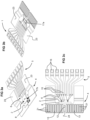
- the lead frame arrangement 3 comprises a primary conductor 4 and a plurality of secondary conductors 5.
- the lead frame arrangement is formed from a sheet of conductive metal, more specifically in the form of a band or strip that is stamped and formed in a stamping and forming process to cut out, bend and/or emboss the sheet metal to form the primary and secondary conductors. Stamping and forming of lead frame arrangements from sheet metal are per se well known techniques. Sheet metal used in such arrangements has initially a constant thickness that we shall name herein "base sheet thickness" having a thickness B .
- the primary and secondary conductors comprise generally throughout essentially the base sheet thickness B except for slight variations due to a bending operation if the portions of the conductors are bent out of the original plane of the sheet metal, for instance to form contact terminals.
- the base sheet thickness B is an important characteristic of the mechanical rigidity of the contact terminals especially if they protrude out of the overmold housing. Even in arrangements where the contact terminals are flush with or embedded in the overmold housing such that only a contact pad surface is exposed, the base thickness may be needed at least around connection ends for secure anchoring to the housing and coupling to the external circuit board conductive pad to which it is welded or soldered.
- the thickness of the sheet metal also affects the cross-section of the conductors, in particular the primary conductor and thus the current carrying capability of the conductors of the lead frame arrangement.
- the IC chip 2 also has a certain thickness and the overmold housing 7 molded around the lead frame conductor arrangement 3 and the IC chip 2 also requires a certain thickness to insulate these components from the external environment.
- At least a portion of the secondary conductors 5 has thinned portions of a thickness T that is in a range between 20% and 80% the base thickness B , preferably in a range from 30% to 70%, more preferably in a range from 40% to 60% for reasons that will be described in more detail hereafter.
- the primary conductor comprises a pair of surface mount connection terminals 13 configured for surface mount connection to conductive traces on an external circuit board, and a sensing portion 12 interconnecting the pair of surface mount connection terminals 13.
- the sensing portion 12 comprises a reduced conductive cross-sectional area in order to concentrate for the current to be measured (the primary current) and increase the intensity of the magnetic field around the sensing portion 12.
- the reduced cross-sectional area of the sensing portion 12 may for instance be formed by providing a slot 24 in the primary conductor between the connection terminals 13.
- the IC chip 2 is positioned in a partially overlapping relationship over the sensing portion 12.
- the magnetic field sensing portion 10 of the IC chip is positioned preferably in an overlapping relationship with the sensing portion 12 of the primary conductor so that the magnetic field sensing portion 10 is positioned very close to the sensing portion 12 of the primary conductor.
- An insulating sheet 22 is positioned between a portion of the primary conductor 4 encompassing the sensing portion 12 and the IC chip 9.
- the insulating sheet 8 may for instance be in the form of a sheet of polymeric materials such as polyimide, in single or multiple layers, or may be as well a small sheet of glass that defines the gap between the IC chip active sensing side 9a and the primary conductor, and that provides insulation between the primary conductor and IC chip.
- the insulating sheet 8 extends over the primary conductor 4 to an extent greater than the IC chip 2 to form a border of minimum width W therearound so as to increase the creepage distance between the IC chip and the primary conductor.
- the semi-conductor IC chip only partially overlaps the primary conductor, a portion of the IC chip comprising the connection terminals 11 extending beyond an inner edge 25 of the primary conductor 4 such that the connection portions do not overlap the primary conductor and are accessible for connection to bond wires 6.
- the insulating sheet 8 also advantageously extends beyond the inner edge 25 of the primary conductor such that the foil only partially overlaps the primary conductor, here also to increase the electrical creepage distance between the IC chip 2 and the primary conductor 4.
- the IC chip is oriented such that the active sensing portions faces the primary conductor to be as close as possible to the primary conductor for maximizing the signal measurement.
- the secondary conductors 5 which serve to interconnect the IC chip 2 to power and signal connections of an external circuit to which the current transducer is intended to be connected, comprise a plurality of conductors formed from the lead frame arrangement as previously discussed, each secondary conductor comprising an IC connection portion 15 on one end and the surface mount connection terminal 16 at the other end.
- the surface mount connection terminal 16 may be for instance arranged in a row presenting contact pads intended for surface mount solder or welding connection, as per se known in the art, to circuit traces of an external circuit board.
- the surface mount connection terminals 16 are thus positioned proximate an outer edge of the transducer overmold housing 7, the IC connection portions 15 being positioned proximate the IC chip 2 allowing bond wire connections between the IC chip 2 and the IC connection portions 15 of the secondary conductors.
- the IC connection portions 15 of the secondary conductors are spaced closer together than the surface mount connection terminals 13 that fan outwardly from the IC connection portions.
- Bond wires 6 are connected between the IC connection portions 15 of each secondary conductor 5 and connection terminals 11 on the IC chip 2. It may be noted that certain secondary conductors may have no connection to the IC chip, forming a redundant secondary conductor for use with semi-conductor chips with more connection portions. In other words, the number of connections depend on the functions incorporated in the IC chip.
- the lead frame conductor arrangement 3 may have a constant configuration, whereas the number of wire bond interconnections between the secondary conductors and IC chip may depend on the configuration of the IC chip and desired functionalities to be incorporated in the transducer.
- At least a portion of the secondary conductors encompassing the IC connection portions 15 have a thinned portion of reduced thickness T that, as previously mentioned, is in a range of 20% to 80% of base thickness B preferably in a range of 30% to 70%m more preferably in a range of 40% to 60%.
- the reduced thickness of the IC connection portions 15 allows the bond wires 6 to have a reduced loop height with respect to the outermost surface 26 of the lead frame arrangement 3 facing away from the IC chip 2, thus allowing a lower overall height H of the overmold housing 7.
- the bond wire 6 may have a portion that extends above the recess. Nevertheless, the portion extending above the recess will be less than in conventional arrangements in which the loop of the bond wire will be yet further distanced from the outer surface of the lead frame.
- the bond wires 6 are mounted and connected to the IC chip 2 and secondary conductors 5 on the same side of the transducer as the surface mount connection terminals 13 of the primary conductor 4 and the surface mount connection terminals 16 of the secondary conductors 5.
- the surface mount connection terminals 13, 16 may be embossed or stamped in an offset plane from a plane of the lead frame arrangement including the IC connection portions 15 of the secondary conductors so as to present terminals flush with or extending beyond a mounting side surface 27 of the overmold housing 7.
- the lead frame may be plated as well with any suitable wire bondable layer in accordance with the bond wire used.
- the thinned portion thickness T of the lead frame arrangement surrounding at least the IC connection portions 15 of the secondary conductors may be formed by an etching process, for instance a chemical or laser etching process, such processes being per se known in the field of etching metallic conductive materials.
- Other process examples may comprise coining or embossing.
- the thinned portion thickness T may extend over a large portion of the lead frame arrangement, including up to all of the lead frame arrangement except for the surface mount connection terminals 13, 16 of the primary and secondary conductors.
- the surface mount connection terminals 13 of the primary conductor may advantageously comprise a plurality of ridge portions 21 that may, for instance be embossed by stamping of the sheet metal or may be formed in an etching process out of the base thickness of the sheet metal.
- the ridge portions 21 advantageously improve the solder connection to complementary circuit traces on an external circuit board, to improve the mechanical and electrical connection between the primary conductor and the circuit traces on the external circuit board.
- the improved connection may also improve thermal transfer when the current transducer is used for measurement of high intensity currents (relative to the size of the transducer).
- the connection portions 13 may comprise only a few or only a single connection pad per connection side.
- the primary conductor 4 may further comprise extensions 23 extending from the surface mount connection terminals 13, that serve as a heat sink and that may optionally be configured for thermal coupling to an external heat sink.
- the heat sink may also be simply integrated in the current transducer forming a large surface to improve heat transfer out of the primary conductor when large currents (relative to the size of the transducer) are flowing through the transducer.
Landscapes
- Physics & Mathematics (AREA)
- General Physics & Mathematics (AREA)
- Lead Frames For Integrated Circuits (AREA)
- Measuring Instrument Details And Bridges, And Automatic Balancing Devices (AREA)
Description
- The present invention relates to an open-loop current transducer for surface mounting on a circuit board.
- It is known to provide open-loop current transducers having surface mount electrical connections for mounting on a circuit board. In many applications, there is an advantage in having a very compact and low height current transducer having an integrated primary conductor within an overmolded insulative housing. Such coreless current transducers may include an integrated circuit (IC) chip having an active sensing layer thereon detecting the magnetic field induced by a current to be measured flowing in a primary conductor integrated within the current transducer, the integrated circuit chip being electrically connected to secondary contacts that supply power and allow transmission of the measurement signal to the external circuit board.
- It is well known to form the primary and secondary conductors from a lead frame. A lead frame is a strip of sheet metal that is stamped and formed to cut out primary and secondary contacts from the sheet metal, the contacts and integrated circuit being overmolded by an insulating polymer, connection ends of the contacts being exposed and configured for a solder or welding connection to circuit traces on the circuit board.
- The electrical interconnection between the integrated circuit and the secondary contacts may be connected by a so-called "flip-chip" connection or by wire bonding. Active portions and connection interfaces on the semi-conductor substrate which, for instance a CMOS IC, are typically provided on a same single side of the IC. A flip-chip arrangement, for instance as described in
US 2006/219436 A1 , allows the active side to be facing and adjacent the lead frame conductor arrangement, allowing electrical interconnection between the lead frame and connection portions on the integrated circuit active surface, while at the same time having the active sensing portion of the integrated circuit being very close to the primary conductor. This provides greater sensitivity for measurement of the primary current due to the very small distance between the sensing layer and the primary conductor. Flip-chip connections can however be costly and complex to manufacture because of the small distances on the IC chip between connection points that need to be directly connected to the secondary conductors of the lead frame arrangement. There may also be disadvantages regarding electrical creepage distances that are more difficult to manage than in wire bond interconnections. - Wire bonding is a very common and widely used technique for interconnecting integrated circuits to conductors forming connection terminals for the IC chip. In conventional current transducers, a drawback of wire bonding interconnections between the IC chip and the lead frame arrangement is however the increased height compared to flip-chip arrangements due to the height of the interconnecting wire loops between the IC substrate and the lead frame conductors. Also, in conventional current transducers with wire bonding between the lead frame and IC chip, for instance as described in
US 2016/ 282388 A1 , the active sensor side faces away from the lead frame conductor arrangement in order to have the active surface accessible for the wire bonding between the lead frame terminals and the connection points on the IC circuit. There is thus a lower sensitivity compared to a flip-chip arrangement. - In view of the foregoing, it is an object of the present invention is to overcome the drawbacks of both conventional flip-chip and conventional wire bonded arrangements in open-loop current transducers for surface mount on circuit boards. In particular, it is an object of the invention to provide an open-loop current transducer for surface mounting on a circuit board that has a low height and high measurement sensitivity, yet that is economical to manufacture.
- It is advantageous to provide an open-loop surface mount current transducer that is reliable, in particular ensuring good insulation properties between the IC chip and the integrated primary conductor.
- Objects of the invention have been achieved by providing an open loop current transducer according to
claim 1. - Disclosed herein is an open-loop electrical current transducer for surface mounting on an external circuit board, comprising an integrated circuit (IC) chip comprising
- a magnetic field sensing portion and connection terminals on a first active side of the IC chip,
- a lead frame arrangement comprising a primary conductor and a plurality of secondary conductors comprising IC connection portions,
- a plurality of bond wires interconnecting the IC connection portions to the connection terminals of the IC chip, and
- an insulating overmold housing overmolded over the IC chip, the bond wires, and a portion of the lead frame arrangement.
- The lead frame arrangement is formed from sheet metal having a base sheet of thickness B wherein at least portions of the lead frame arrangement comprise a thickness equal to said base sheet thickness B. The first active side of the IC chip faces the lead frame arrangement and at least a portion of the lead frame arrangement comprises a thinned portion of thickness T between 20% and 80% of the base sheet thickness B, said thinned portion of thickness T including said IC connection portions of the secondary conductors .
- In an advantageous embodiment, the IC chip is mounted partially overlapping a portion of the primary conductor including a sensing portion of the primary conductor, an insulating sheet mounted between the IC chip and primary conductor made of a material different from a material forming the insulating overmold housing, the connection terminals of the IC chip being provided on said portion of the IC chip not overlapping the primary conductor.
- In an advantageous embodiment, said insulating foil extends beyond the portion of IC chip overlapping the primary conductor with a border of non-zero width W for increasing an electrical creepage distance between the primary conductor and IC chip.
- In an advantageous embodiment, said insulating foil extends beyond an edge of the primary conductor over which the IC chip also extends in order to increase the creepage distance between the IC chip and the primary conductor.
- In an advantageous embodiment, the sensing portion has a reduced current carrying cross-sectional area compared to surface mount connection terminals of the primary conductor between which the sensing portion is positioned and interconnected.
- In an advantageous embodiment, the surface mount connection terminals of the primary conductor comprise a plurality of ridge portions.
- In an advantageous embodiment, surface mount connection terminals of the secondary conductors are arranged in a row along a first edge of the overmold housing and the surface mount connection terminals of the primary conductor are arranged adjacent an opposed edge of the overmold housing.
- In an advantageous embodiment, the thinned portion thickness T is in the range of 30% to 70% of base sheet thickness B. Preferably the thinned portion thickness T is in the range of 40% to 60% of base sheet thickness B.
- In an advantageous embodiment, the primary conductor comprises one or more heat sink extensions serving as heat sinks extending from the surface mount connection terminals thereof.
- In an advantageous embodiment, the one or more heat sink extensions extend from the primary conductor surface mount connection terminals towards the surface mount connection terminals of the secondary conductors.
- In an advantageous embodiment, there are a pair of heat sink extensions, one for extending from each surface mount connection terminal of the primary conductor
- Further objects and advantageous features of the invention will be apparent from the claims, from the detailed description, and annexed drawings, in which:
-
Figures 1a to 1c are perspective views of a surface mount open-loop current transducer according to an embodiment of the invention,figure 1c showing an overmold housing portion partially cut away; -
Figure 2 is a schematic cross-sectional view of a current transducer according to an embodiment of the invention; -
Figures 3a and 3b are perspective views andfigure 3c is a plan view of the current transducer offigures 1a to 1c with the overmold housing removed; -
Figure 4a is a plan view andfigure 4b a perspective view of another embodiment of the current transducer according to the invention, with the overmold housing removed, andfigure 4c is an enlarged view of a portion offigure 4a . - Referring to the figures, an
electric current transducer 1 for surface mount connection on an external circuit board comprises amagnetic field sensor 2 connected to alead frame arrangement 3 housed within an insulating overmoldhousing 7. - The
magnetic field sensor 2 is in the form of an integrated circuit (IC) chip having a firstactive side 9a and asecond side 9b, at least the firstactive side 9a having active portions includingelectrical connection terminals 11 for connection to power and signal transmission conductors and a magneticfield sensor portion 10 arranged at or close to the surface of the first side. The chip may be attached to the lead frame with a glue layer between theface 9a and theinsulating layer 8. Theinsulating layer 8 may be attached to the lead frame with a glue layer. - The magnetic
field sensing portion 10 may comprise a Hall effect sensor, or a giant magnetoresistive sensor or other forms of magnetic field sensors that are per se well known in the art. TheIC chip 2 may for instance be in the form of a CMOS chip although other types of semi-conductor integrated circuit chips with magnetic field sensing portions per se known in the art may be used. The semi-conductor chip does not need to be further described, such semi-conductor chips with magnetic field sensing portions and connection terminals being per se well known in the art. - The
lead frame arrangement 3 comprises aprimary conductor 4 and a plurality ofsecondary conductors 5. The lead frame arrangement is formed from a sheet of conductive metal, more specifically in the form of a band or strip that is stamped and formed in a stamping and forming process to cut out, bend and/or emboss the sheet metal to form the primary and secondary conductors. Stamping and forming of lead frame arrangements from sheet metal are per se well known techniques. Sheet metal used in such arrangements has initially a constant thickness that we shall name herein "base sheet thickness" having a thickness B. In conventional lead frame arrangements stamped and formed from sheet metal, the primary and secondary conductors comprise generally throughout essentially the base sheet thickness B except for slight variations due to a bending operation if the portions of the conductors are bent out of the original plane of the sheet metal, for instance to form contact terminals. The base sheet thickness B is an important characteristic of the mechanical rigidity of the contact terminals especially if they protrude out of the overmold housing. Even in arrangements where the contact terminals are flush with or embedded in the overmold housing such that only a contact pad surface is exposed, the base thickness may be needed at least around connection ends for secure anchoring to the housing and coupling to the external circuit board conductive pad to which it is welded or soldered. The thickness of the sheet metal also affects the cross-section of the conductors, in particular the primary conductor and thus the current carrying capability of the conductors of the lead frame arrangement. - The
IC chip 2 also has a certain thickness and the overmoldhousing 7 molded around the leadframe conductor arrangement 3 and theIC chip 2 also requires a certain thickness to insulate these components from the external environment. - There is however a desire to have a transducer with a very low height H for integration on a circuit board since in many applications the overall height of the electronic components which include the circuit board should be as small as possible.
- According to the invention, at least a portion of the
secondary conductors 5 has thinned portions of a thickness T that is in a range between 20% and 80% the base thickness B, preferably in a range from 30% to 70%, more preferably in a range from 40% to 60% for reasons that will be described in more detail hereafter. - The primary conductor comprises a pair of surface
mount connection terminals 13 configured for surface mount connection to conductive traces on an external circuit board, and asensing portion 12 interconnecting the pair of surfacemount connection terminals 13. Thesensing portion 12 comprises a reduced conductive cross-sectional area in order to concentrate for the current to be measured (the primary current) and increase the intensity of the magnetic field around thesensing portion 12. The reduced cross-sectional area of thesensing portion 12 may for instance be formed by providing aslot 24 in the primary conductor between theconnection terminals 13. - The
IC chip 2 is positioned in a partially overlapping relationship over thesensing portion 12. In particular, the magneticfield sensing portion 10 of the IC chip is positioned preferably in an overlapping relationship with thesensing portion 12 of the primary conductor so that the magneticfield sensing portion 10 is positioned very close to thesensing portion 12 of the primary conductor. - An insulating sheet 22 is positioned between a portion of the
primary conductor 4 encompassing thesensing portion 12 and the IC chip 9. The insulatingsheet 8 may for instance be in the form of a sheet of polymeric materials such as polyimide, in single or multiple layers, or may be as well a small sheet of glass that defines the gap between the IC chipactive sensing side 9a and the primary conductor, and that provides insulation between the primary conductor and IC chip. The insulatingsheet 8 extends over theprimary conductor 4 to an extent greater than theIC chip 2 to form a border of minimum width W therearound so as to increase the creepage distance between the IC chip and the primary conductor. The semi-conductor IC chip only partially overlaps the primary conductor, a portion of the IC chip comprising theconnection terminals 11 extending beyond aninner edge 25 of theprimary conductor 4 such that the connection portions do not overlap the primary conductor and are accessible for connection tobond wires 6. The insulatingsheet 8 also advantageously extends beyond theinner edge 25 of the primary conductor such that the foil only partially overlaps the primary conductor, here also to increase the electrical creepage distance between theIC chip 2 and theprimary conductor 4. The IC chip is oriented such that the active sensing portions faces the primary conductor to be as close as possible to the primary conductor for maximizing the signal measurement. - The
secondary conductors 5 which serve to interconnect theIC chip 2 to power and signal connections of an external circuit to which the current transducer is intended to be connected, comprise a plurality of conductors formed from the lead frame arrangement as previously discussed, each secondary conductor comprising anIC connection portion 15 on one end and the surfacemount connection terminal 16 at the other end. The surfacemount connection terminal 16 may be for instance arranged in a row presenting contact pads intended for surface mount solder or welding connection, as per se known in the art, to circuit traces of an external circuit board. The surfacemount connection terminals 16 are thus positioned proximate an outer edge of the transducer overmoldhousing 7, theIC connection portions 15 being positioned proximate theIC chip 2 allowing bond wire connections between theIC chip 2 and theIC connection portions 15 of the secondary conductors. TheIC connection portions 15 of the secondary conductors are spaced closer together than the surfacemount connection terminals 13 that fan outwardly from the IC connection portions. -
Bond wires 6 are connected between theIC connection portions 15 of eachsecondary conductor 5 andconnection terminals 11 on theIC chip 2. It may be noted that certain secondary conductors may have no connection to the IC chip, forming a redundant secondary conductor for use with semi-conductor chips with more connection portions. In other words, the number of connections depend on the functions incorporated in the IC chip. The leadframe conductor arrangement 3 may have a constant configuration, whereas the number of wire bond interconnections between the secondary conductors and IC chip may depend on the configuration of the IC chip and desired functionalities to be incorporated in the transducer. - According to the invention, at least a portion of the secondary conductors encompassing the
IC connection portions 15 have a thinned portion of reduced thickness T that, as previously mentioned, is in a range of 20% to 80% of base thickness B preferably in a range of 30% to 70%m more preferably in a range of 40% to 60%. The reduced thickness of theIC connection portions 15 allows thebond wires 6 to have a reduced loop height with respect to theoutermost surface 26 of thelead frame arrangement 3 facing away from theIC chip 2, thus allowing a lower overall height H of theovermold housing 7. Although in the schematically illustrated embodiment offigure 2 , the loop height of the bond wire is fully within the recess formed by the thinned portion T, thebond wire 6 may have a portion that extends above the recess. Nevertheless, the portion extending above the recess will be less than in conventional arrangements in which the loop of the bond wire will be yet further distanced from the outer surface of the lead frame. Advantageously also, thebond wires 6 are mounted and connected to theIC chip 2 andsecondary conductors 5 on the same side of the transducer as the surfacemount connection terminals 13 of theprimary conductor 4 and the surfacemount connection terminals 16 of thesecondary conductors 5. - The surface
mount connection terminals IC connection portions 15 of the secondary conductors so as to present terminals flush with or extending beyond a mountingside surface 27 of theovermold housing 7. The lead frame may be plated as well with any suitable wire bondable layer in accordance with the bond wire used. - The thinned portion thickness T of the lead frame arrangement surrounding at least the
IC connection portions 15 of the secondary conductors may be formed by an etching process, for instance a chemical or laser etching process, such processes being per se known in the field of etching metallic conductive materials. Other process examples may comprise coining or embossing. - It may be noted that the thinned portion thickness T may extend over a large portion of the lead frame arrangement, including up to all of the lead frame arrangement except for the surface
mount connection terminals - In embodiments, the surface
mount connection terminals 13 of the primary conductor may advantageously comprise a plurality ofridge portions 21 that may, for instance be embossed by stamping of the sheet metal or may be formed in an etching process out of the base thickness of the sheet metal. Theridge portions 21 advantageously improve the solder connection to complementary circuit traces on an external circuit board, to improve the mechanical and electrical connection between the primary conductor and the circuit traces on the external circuit board. The improved connection may also improve thermal transfer when the current transducer is used for measurement of high intensity currents (relative to the size of the transducer). Nevertheless, in variants theconnection portions 13 may comprise only a few or only a single connection pad per connection side. - The
primary conductor 4 may further compriseextensions 23 extending from the surfacemount connection terminals 13, that serve as a heat sink and that may optionally be configured for thermal coupling to an external heat sink. The heat sink may also be simply integrated in the current transducer forming a large surface to improve heat transfer out of the primary conductor when large currents (relative to the size of the transducer) are flowing through the transducer. -
- electric
current transducer 1- magnetic field sensor 2 (integrated circuit (IC) chip)
- first side (active sensing side) 9a
- magnetic
field sensing portion 10 -
connection terminals 11 -
second side 9b
- magnetic
- first side (active sensing side) 9a
-
Lead frame arrangement 3-
primary conductor 4- sensing
portion 12 -
slot 24 -
inner edge 25 - surface
mount connection terminals 13
ridge portions 21
- sensing
-
secondary conductors 5-
IC connection portion 15 - surface
mount connection terminals 16
-
- first (bonding wire)
side 17a - second (die mounting)
side 17b - base sheet portion 18
- thinned portion 19
bond wire connection recess 20
etched recess
-
- Insulating
sheet 8 -
Bond wires 6 -
Overmold housing 7
mountingside surface 27
- magnetic field sensor 2 (integrated circuit (IC) chip)
- base sheet thickness B
- thinned portion thickness T
- recess thickness R
Claims (12)
- An open-loop electrical current transducer (1) for surface mounting on an external circuit board, comprising an integrated circuit, IC, chip (2) comprising a magnetic field sensing portion (10) and connection terminals (11) on a first active side (9a) of the IC chip, a lead frame arrangement (3) comprising a primary conductor (4) and a plurality of secondary conductors (5) comprising IC connection portions (15), a plurality of bond wires (6) interconnecting the IC connection portions (15) to the connection terminals (11) of the IC chip, and an insulating overmold housing (7) overmolded over the IC chip, the bond wires, and a portion of the lead frame arrangement, the lead frame arrangement formed from sheet metal having a base sheet of thickness B wherein at least portions of the lead frame arrangement comprise a thickness equal to said base sheet thickness B, wherein at least a portion of the lead frame arrangement comprises a thinned portion of thickness T between 20% and 80% of the base sheet thickness B, said thinned portion of thickness T including said IC connection portions (15) of the secondary conductors (5),
characterized in that the first active side of the IC chip faces the lead frame arrangement. - Current transducer according to the preceding claim wherein the IC chip is mounted partially overlapping a sensing portion (12) of the primary conductor, wherein an insulating sheet (8) mounted between the IC chip and the primary conductor is made of a material different from a material forming the insulating overmold housing, the connection terminals (11) of the IC chip being provided on the portion of the IC chip not overlapping the primary conductor.
- Current transducer according to the preceding claim wherein said insulating sheet extends beyond the portion of the IC chip overlapping the primary conductor with a border of non-zero width W for increasing an electrical creepage distance between the primary conductor and the IC chip.
- Current transducer according to the preceding claim, wherein said insulating foil extends beyond an edge (25) of the primary conductor over which the IC chip also extends in order to increase the creepage distance between the IC chip and the primary conductor.
- Current transducer according to any preceding claim 2-4 wherein the sensing portion (12) has a reduced current carrying cross-sectional area compared to surface mount connection terminals (13) of the primary conductor.
- Current transducer according to the preceding claim wherein the surface mount connection terminals (13) of the primary conductor comprise a plurality of ridge portions (21).
- Current transducer according to either of the two directly preceding claims wherein surface mount connection terminals (16) of the secondary conductors (5) are arranged in a row along a first edge of the overmold housing (7) and the surface mount connection terminals (13) of the primary conductor are arranged adjacent an opposed edge of the overmold housing.
- Current transducer according to any preceding claim wherein the thinned portion thickness T is in the range of 30% to 70% of the base sheet thickness B.
- Current transducer according to the preceding claim wherein the thinned portion thickness T is in the range of 40% to 60% of the base sheet thickness B.
- Current transducer according to any preceding claim 5-7 wherein the primary conductor (4) comprises one or more heat sink extensions (23) serving as heat sinks extending from the surface mount connection terminals (13) thereof.
- Current transducer according to the preceding claim wherein the one or more heat sink extensions extend from the primary conductor surface mount connection terminals (13) towards the surface mount connection terminals (16) of the secondary conductors (5).
- Current transducer according to either of the two directly preceding claims wherein there are a pair of said heat sink extensions, one for extending from each surface mount connection terminal (13) of the primary conductor.
Applications Claiming Priority (2)
| Application Number | Priority Date | Filing Date | Title |
|---|---|---|---|
| EP20187682.8A EP3943952A1 (en) | 2020-07-24 | 2020-07-24 | Current transducer |
| PCT/EP2021/069363 WO2022017857A1 (en) | 2020-07-24 | 2021-07-12 | Current transducer |
Publications (3)
| Publication Number | Publication Date |
|---|---|
| EP4185877A1 EP4185877A1 (en) | 2023-05-31 |
| EP4185877B1 true EP4185877B1 (en) | 2025-05-14 |
| EP4185877C0 EP4185877C0 (en) | 2025-05-14 |
Family
ID=71833165
Family Applications (2)
| Application Number | Title | Priority Date | Filing Date |
|---|---|---|---|
| EP20187682.8A Withdrawn EP3943952A1 (en) | 2020-07-24 | 2020-07-24 | Current transducer |
| EP21740559.6A Active EP4185877B1 (en) | 2020-07-24 | 2021-07-12 | Current transducer |
Family Applications Before (1)
| Application Number | Title | Priority Date | Filing Date |
|---|---|---|---|
| EP20187682.8A Withdrawn EP3943952A1 (en) | 2020-07-24 | 2020-07-24 | Current transducer |
Country Status (5)
| Country | Link |
|---|---|
| US (1) | US12196787B2 (en) |
| EP (2) | EP3943952A1 (en) |
| JP (1) | JP7650956B2 (en) |
| CN (1) | CN116171387A (en) |
| WO (1) | WO2022017857A1 (en) |
Families Citing this family (3)
| Publication number | Priority date | Publication date | Assignee | Title |
|---|---|---|---|---|
| EP4375678B1 (en) * | 2022-11-28 | 2025-12-24 | LEM International SA | Integrated circuit current transducer |
| US20240258211A1 (en) * | 2023-01-26 | 2024-08-01 | Texas Instruments Incorporated | Semiconductor device package with isolation |
| EP4624943B1 (en) * | 2024-03-25 | 2025-12-24 | LEM International SA | Current transducer with integrated circuit and leadframe conductor arrangement |
Family Cites Families (19)
| Publication number | Priority date | Publication date | Assignee | Title |
|---|---|---|---|---|
| US6853178B2 (en) * | 2000-06-19 | 2005-02-08 | Texas Instruments Incorporated | Integrated circuit leadframes patterned for measuring the accurate amplitude of changing currents |
| US20060219436A1 (en) * | 2003-08-26 | 2006-10-05 | Taylor William P | Current sensor |
| US7075287B1 (en) * | 2003-08-26 | 2006-07-11 | Allegro Microsystems, Inc. | Current sensor |
| US20080013298A1 (en) | 2006-07-14 | 2008-01-17 | Nirmal Sharma | Methods and apparatus for passive attachment of components for integrated circuits |
| US20110006763A1 (en) * | 2009-07-07 | 2011-01-13 | Anthonius Bakker | Hall effect current sensor system and associated flip-chip packaging |
| US8760149B2 (en) * | 2010-04-08 | 2014-06-24 | Infineon Technologies Ag | Magnetic field current sensors |
| US8907437B2 (en) | 2011-07-22 | 2014-12-09 | Allegro Microsystems, Llc | Reinforced isolation for current sensor with magnetic field transducer |
| US9190606B2 (en) * | 2013-03-15 | 2015-11-17 | Allegro Micosystems, LLC | Packaging for an electronic device |
| US10345343B2 (en) * | 2013-03-15 | 2019-07-09 | Allegro Microsystems, Llc | Current sensor isolation |
| JP6234263B2 (en) | 2014-02-12 | 2017-11-22 | 旭化成エレクトロニクス株式会社 | Current sensor |
| EP3159705A1 (en) * | 2015-10-23 | 2017-04-26 | LEM Intellectual Property SA | Current transducer with integrated primary conductor |
| US9810721B2 (en) * | 2015-12-23 | 2017-11-07 | Melexis Technologies Sa | Method of making a current sensor and current sensor |
| JP2017134022A (en) | 2016-01-29 | 2017-08-03 | 旭化成エレクトロニクス株式会社 | Electric current sensor and manufacturing method |
| WO2018051575A1 (en) | 2016-09-14 | 2018-03-22 | 旭化成エレクトロニクス株式会社 | Electric current sensor |
| US9958482B1 (en) * | 2016-12-20 | 2018-05-01 | Allegro Microsystems, Llc | Systems and methods for a high isolation current sensor |
| CN106653999A (en) * | 2016-12-22 | 2017-05-10 | 上海南麟电子股份有限公司 | Single-chip Hall current sensor and preparation method thereof |
| US10074713B1 (en) * | 2017-09-15 | 2018-09-11 | Allegro Microsystems, Llc | Signal isolator integrated circuit package |
| JP2020095029A (en) * | 2018-12-12 | 2020-06-18 | メレキシス テクノロジーズ エス エーMelexis Technologies SA | Current sensor |
| US11519946B1 (en) * | 2021-08-23 | 2022-12-06 | Allegro Microsystems, Llc | Packaged current sensor integrated circuit |
-
2020
- 2020-07-24 EP EP20187682.8A patent/EP3943952A1/en not_active Withdrawn
-
2021
- 2021-07-12 CN CN202180059801.3A patent/CN116171387A/en active Pending
- 2021-07-12 EP EP21740559.6A patent/EP4185877B1/en active Active
- 2021-07-12 WO PCT/EP2021/069363 patent/WO2022017857A1/en not_active Ceased
- 2021-07-12 JP JP2023504583A patent/JP7650956B2/en active Active
- 2021-07-12 US US18/017,251 patent/US12196787B2/en active Active
Also Published As
| Publication number | Publication date |
|---|---|
| JP2023534866A (en) | 2023-08-14 |
| JP7650956B2 (en) | 2025-03-25 |
| US12196787B2 (en) | 2025-01-14 |
| EP4185877A1 (en) | 2023-05-31 |
| EP4185877C0 (en) | 2025-05-14 |
| CN116171387A (en) | 2023-05-26 |
| EP3943952A1 (en) | 2022-01-26 |
| WO2022017857A1 (en) | 2022-01-27 |
| US20230288453A1 (en) | 2023-09-14 |
Similar Documents
| Publication | Publication Date | Title |
|---|---|---|
| EP4185877B1 (en) | Current transducer | |
| KR100300665B1 (en) | Resin-sealed semiconductor device, circuit member used therefor and method of manufacturing resin-sealed semiconductor device | |
| US6646335B2 (en) | Flexible tape carrier with external terminals formed on interposers | |
| JP3939429B2 (en) | Semiconductor device | |
| US4949225A (en) | Circuit board for mounting electronic components | |
| US7687893B2 (en) | Semiconductor package having leadframe with exposed anchor pads | |
| CN113161300A (en) | Semiconductor packaging structure | |
| US5704593A (en) | Film carrier tape for semiconductor package and semiconductor device employing the same | |
| EP4375678B1 (en) | Integrated circuit current transducer | |
| JP7420640B2 (en) | Current sensor and current sensor manufacturing method | |
| EP4624943B1 (en) | Current transducer with integrated circuit and leadframe conductor arrangement | |
| KR19980063740A (en) | Multilayer Leadframe for Molded Packages | |
| CN120813846A (en) | Magnetic field gradient sensor and current sensor having the same | |
| KR101463074B1 (en) | Leadless package | |
| JP4122560B2 (en) | Semiconductor device and mounting structure of semiconductor device | |
| KR100668932B1 (en) | Lead frame and semiconductor package using same | |
| WO2025124947A1 (en) | Current transducer with leadframe conductors and sensor die for circuit board mounting | |
| KR100705248B1 (en) | Semiconductor package and manufacturing method | |
| JP3586867B2 (en) | Semiconductor device, method of manufacturing the same, method of mounting the same, and circuit board mounting the same | |
| JPH065701B2 (en) | Lead frame and method of manufacturing semiconductor device using the same | |
| JPH1012782A (en) | Hybrid integrated circuit device and method of manufacturing the same | |
| US20090294975A1 (en) | Package for a Die | |
| KR20030029290A (en) | Diode package | |
| JP2000031321A (en) | Structure and manufacturing method of semiconductor device | |
| JPH09232378A (en) | Structure with semiconductor chip |
Legal Events
| Date | Code | Title | Description |
|---|---|---|---|
| STAA | Information on the status of an ep patent application or granted ep patent |
Free format text: STATUS: UNKNOWN |
|
| STAA | Information on the status of an ep patent application or granted ep patent |
Free format text: STATUS: THE INTERNATIONAL PUBLICATION HAS BEEN MADE |
|
| PUAI | Public reference made under article 153(3) epc to a published international application that has entered the european phase |
Free format text: ORIGINAL CODE: 0009012 |
|
| STAA | Information on the status of an ep patent application or granted ep patent |
Free format text: STATUS: REQUEST FOR EXAMINATION WAS MADE |
|
| 17P | Request for examination filed |
Effective date: 20230203 |
|
| AK | Designated contracting states |
Kind code of ref document: A1 Designated state(s): AL AT BE BG CH CY CZ DE DK EE ES FI FR GB GR HR HU IE IS IT LI LT LU LV MC MK MT NL NO PL PT RO RS SE SI SK SM TR |
|
| DAV | Request for validation of the european patent (deleted) | ||
| DAX | Request for extension of the european patent (deleted) | ||
| RIN1 | Information on inventor provided before grant (corrected) |
Inventor name: CLAEYS, STEPHANE Inventor name: ZIGLIOLI, FEDERICO GIOVANNI |
|
| GRAP | Despatch of communication of intention to grant a patent |
Free format text: ORIGINAL CODE: EPIDOSNIGR1 |
|
| STAA | Information on the status of an ep patent application or granted ep patent |
Free format text: STATUS: GRANT OF PATENT IS INTENDED |
|
| INTG | Intention to grant announced |
Effective date: 20250225 |
|
| GRAS | Grant fee paid |
Free format text: ORIGINAL CODE: EPIDOSNIGR3 |
|
| GRAA | (expected) grant |
Free format text: ORIGINAL CODE: 0009210 |
|
| STAA | Information on the status of an ep patent application or granted ep patent |
Free format text: STATUS: THE PATENT HAS BEEN GRANTED |
|
| AK | Designated contracting states |
Kind code of ref document: B1 Designated state(s): AL AT BE BG CH CY CZ DE DK EE ES FI FR GB GR HR HU IE IS IT LI LT LU LV MC MK MT NL NO PL PT RO RS SE SI SK SM TR |
|
| REG | Reference to a national code |
Ref country code: GB Ref legal event code: FG4D |
|
| REG | Reference to a national code |
Ref country code: CH Ref legal event code: EP |
|
| REG | Reference to a national code |
Ref country code: IE Ref legal event code: FG4D |
|
| U01 | Request for unitary effect filed |
Effective date: 20250514 |
|
| U07 | Unitary effect registered |
Designated state(s): AT BE BG DE DK EE FI FR IT LT LU LV MT NL PT RO SE SI Effective date: 20250520 |
|
| U20 | Renewal fee for the european patent with unitary effect paid |
Year of fee payment: 5 Effective date: 20250520 |
|
| PG25 | Lapsed in a contracting state [announced via postgrant information from national office to epo] |
Ref country code: ES Free format text: LAPSE BECAUSE OF FAILURE TO SUBMIT A TRANSLATION OF THE DESCRIPTION OR TO PAY THE FEE WITHIN THE PRESCRIBED TIME-LIMIT Effective date: 20250514 |
|
| PG25 | Lapsed in a contracting state [announced via postgrant information from national office to epo] |
Ref country code: GR Free format text: LAPSE BECAUSE OF FAILURE TO SUBMIT A TRANSLATION OF THE DESCRIPTION OR TO PAY THE FEE WITHIN THE PRESCRIBED TIME-LIMIT Effective date: 20250815 Ref country code: NO Free format text: LAPSE BECAUSE OF FAILURE TO SUBMIT A TRANSLATION OF THE DESCRIPTION OR TO PAY THE FEE WITHIN THE PRESCRIBED TIME-LIMIT Effective date: 20250814 |
|
| PG25 | Lapsed in a contracting state [announced via postgrant information from national office to epo] |
Ref country code: PL Free format text: LAPSE BECAUSE OF FAILURE TO SUBMIT A TRANSLATION OF THE DESCRIPTION OR TO PAY THE FEE WITHIN THE PRESCRIBED TIME-LIMIT Effective date: 20250514 |
|
| PG25 | Lapsed in a contracting state [announced via postgrant information from national office to epo] |
Ref country code: HR Free format text: LAPSE BECAUSE OF FAILURE TO SUBMIT A TRANSLATION OF THE DESCRIPTION OR TO PAY THE FEE WITHIN THE PRESCRIBED TIME-LIMIT Effective date: 20250514 |
|
| PGFP | Annual fee paid to national office [announced via postgrant information from national office to epo] |
Ref country code: CH Payment date: 20250801 Year of fee payment: 5 |
|
| PG25 | Lapsed in a contracting state [announced via postgrant information from national office to epo] |
Ref country code: RS Free format text: LAPSE BECAUSE OF FAILURE TO SUBMIT A TRANSLATION OF THE DESCRIPTION OR TO PAY THE FEE WITHIN THE PRESCRIBED TIME-LIMIT Effective date: 20250814 |
|
| PG25 | Lapsed in a contracting state [announced via postgrant information from national office to epo] |
Ref country code: IS Free format text: LAPSE BECAUSE OF FAILURE TO SUBMIT A TRANSLATION OF THE DESCRIPTION OR TO PAY THE FEE WITHIN THE PRESCRIBED TIME-LIMIT Effective date: 20250914 |
|
| PG25 | Lapsed in a contracting state [announced via postgrant information from national office to epo] |
Ref country code: SM Free format text: LAPSE BECAUSE OF FAILURE TO SUBMIT A TRANSLATION OF THE DESCRIPTION OR TO PAY THE FEE WITHIN THE PRESCRIBED TIME-LIMIT Effective date: 20250514 |
|
| PG25 | Lapsed in a contracting state [announced via postgrant information from national office to epo] |
Ref country code: CZ Free format text: LAPSE BECAUSE OF FAILURE TO SUBMIT A TRANSLATION OF THE DESCRIPTION OR TO PAY THE FEE WITHIN THE PRESCRIBED TIME-LIMIT Effective date: 20250514 |
|
| PG25 | Lapsed in a contracting state [announced via postgrant information from national office to epo] |
Ref country code: SK Free format text: LAPSE BECAUSE OF FAILURE TO SUBMIT A TRANSLATION OF THE DESCRIPTION OR TO PAY THE FEE WITHIN THE PRESCRIBED TIME-LIMIT Effective date: 20250514 |
|
| PLBE | No opposition filed within time limit |
Free format text: ORIGINAL CODE: 0009261 |
|
| STAA | Information on the status of an ep patent application or granted ep patent |
Free format text: STATUS: NO OPPOSITION FILED WITHIN TIME LIMIT |