EP4184775A1 - Buck converter with high power efficiency - Google Patents
Buck converter with high power efficiency Download PDFInfo
- Publication number
- EP4184775A1 EP4184775A1 EP22208781.9A EP22208781A EP4184775A1 EP 4184775 A1 EP4184775 A1 EP 4184775A1 EP 22208781 A EP22208781 A EP 22208781A EP 4184775 A1 EP4184775 A1 EP 4184775A1
- Authority
- EP
- European Patent Office
- Prior art keywords
- inductor
- buck converter
- voltage
- switch
- terminal
- Prior art date
- Legal status (The legal status is an assumption and is not a legal conclusion. Google has not performed a legal analysis and makes no representation as to the accuracy of the status listed.)
- Pending
Links
Images


Classifications
-
- H—ELECTRICITY
- H02—GENERATION; CONVERSION OR DISTRIBUTION OF ELECTRIC POWER
- H02M—APPARATUS FOR CONVERSION BETWEEN AC AND AC, BETWEEN AC AND DC, OR BETWEEN DC AND DC, AND FOR USE WITH MAINS OR SIMILAR POWER SUPPLY SYSTEMS; CONVERSION OF DC OR AC INPUT POWER INTO SURGE OUTPUT POWER; CONTROL OR REGULATION THEREOF
- H02M3/00—Conversion of DC power input into DC power output
- H02M3/02—Conversion of DC power input into DC power output without intermediate conversion into AC
- H02M3/04—Conversion of DC power input into DC power output without intermediate conversion into AC by static converters
- H02M3/10—Conversion of DC power input into DC power output without intermediate conversion into AC by static converters using discharge tubes with control electrode or semiconductor devices with control electrode
- H02M3/145—Conversion of DC power input into DC power output without intermediate conversion into AC by static converters using discharge tubes with control electrode or semiconductor devices with control electrode using devices of a triode or transistor type requiring continuous application of a control signal
- H02M3/155—Conversion of DC power input into DC power output without intermediate conversion into AC by static converters using discharge tubes with control electrode or semiconductor devices with control electrode using devices of a triode or transistor type requiring continuous application of a control signal using semiconductor devices only
- H02M3/156—Conversion of DC power input into DC power output without intermediate conversion into AC by static converters using discharge tubes with control electrode or semiconductor devices with control electrode using devices of a triode or transistor type requiring continuous application of a control signal using semiconductor devices only with automatic control of output voltage or current, e.g. switching regulators
- H02M3/158—Conversion of DC power input into DC power output without intermediate conversion into AC by static converters using discharge tubes with control electrode or semiconductor devices with control electrode using devices of a triode or transistor type requiring continuous application of a control signal using semiconductor devices only with automatic control of output voltage or current, e.g. switching regulators including plural semiconductor devices as final control devices for a single load
- H02M3/1582—Buck-boost converters
-
- H—ELECTRICITY
- H02—GENERATION; CONVERSION OR DISTRIBUTION OF ELECTRIC POWER
- H02M—APPARATUS FOR CONVERSION BETWEEN AC AND AC, BETWEEN AC AND DC, OR BETWEEN DC AND DC, AND FOR USE WITH MAINS OR SIMILAR POWER SUPPLY SYSTEMS; CONVERSION OF DC OR AC INPUT POWER INTO SURGE OUTPUT POWER; CONTROL OR REGULATION THEREOF
- H02M3/00—Conversion of DC power input into DC power output
- H02M3/02—Conversion of DC power input into DC power output without intermediate conversion into AC
- H02M3/04—Conversion of DC power input into DC power output without intermediate conversion into AC by static converters
- H02M3/06—Conversion of DC power input into DC power output without intermediate conversion into AC by static converters using resistors or capacitors, e.g. potential divider
- H02M3/07—Conversion of DC power input into DC power output without intermediate conversion into AC by static converters using resistors or capacitors, e.g. potential divider using capacitors charged and discharged alternately by semiconductor devices with control electrode, e.g. charge pumps
-
- H—ELECTRICITY
- H02—GENERATION; CONVERSION OR DISTRIBUTION OF ELECTRIC POWER
- H02M—APPARATUS FOR CONVERSION BETWEEN AC AND AC, BETWEEN AC AND DC, OR BETWEEN DC AND DC, AND FOR USE WITH MAINS OR SIMILAR POWER SUPPLY SYSTEMS; CONVERSION OF DC OR AC INPUT POWER INTO SURGE OUTPUT POWER; CONTROL OR REGULATION THEREOF
- H02M1/00—Details of apparatus for conversion
- H02M1/0048—Circuits or arrangements for reducing losses
-
- H—ELECTRICITY
- H02—GENERATION; CONVERSION OR DISTRIBUTION OF ELECTRIC POWER
- H02M—APPARATUS FOR CONVERSION BETWEEN AC AND AC, BETWEEN AC AND DC, OR BETWEEN DC AND DC, AND FOR USE WITH MAINS OR SIMILAR POWER SUPPLY SYSTEMS; CONVERSION OF DC OR AC INPUT POWER INTO SURGE OUTPUT POWER; CONTROL OR REGULATION THEREOF
- H02M1/00—Details of apparatus for conversion
- H02M1/0048—Circuits or arrangements for reducing losses
- H02M1/0054—Transistor switching losses
-
- H—ELECTRICITY
- H02—GENERATION; CONVERSION OR DISTRIBUTION OF ELECTRIC POWER
- H02M—APPARATUS FOR CONVERSION BETWEEN AC AND AC, BETWEEN AC AND DC, OR BETWEEN DC AND DC, AND FOR USE WITH MAINS OR SIMILAR POWER SUPPLY SYSTEMS; CONVERSION OF DC OR AC INPUT POWER INTO SURGE OUTPUT POWER; CONTROL OR REGULATION THEREOF
- H02M1/00—Details of apparatus for conversion
- H02M1/0095—Hybrid converter topologies, e.g. NPC mixed with flying capacitor, thyristor converter mixed with MMC or charge pump mixed with buck
-
- H—ELECTRICITY
- H02—GENERATION; CONVERSION OR DISTRIBUTION OF ELECTRIC POWER
- H02M—APPARATUS FOR CONVERSION BETWEEN AC AND AC, BETWEEN AC AND DC, OR BETWEEN DC AND DC, AND FOR USE WITH MAINS OR SIMILAR POWER SUPPLY SYSTEMS; CONVERSION OF DC OR AC INPUT POWER INTO SURGE OUTPUT POWER; CONTROL OR REGULATION THEREOF
- H02M1/00—Details of apparatus for conversion
- H02M1/08—Circuits specially adapted for the generation of control voltages for semiconductor devices incorporated in static converters
- H02M1/088—Circuits specially adapted for the generation of control voltages for semiconductor devices incorporated in static converters for the simultaneous control of series or parallel connected semiconductor devices
-
- H—ELECTRICITY
- H02—GENERATION; CONVERSION OR DISTRIBUTION OF ELECTRIC POWER
- H02M—APPARATUS FOR CONVERSION BETWEEN AC AND AC, BETWEEN AC AND DC, OR BETWEEN DC AND DC, AND FOR USE WITH MAINS OR SIMILAR POWER SUPPLY SYSTEMS; CONVERSION OF DC OR AC INPUT POWER INTO SURGE OUTPUT POWER; CONTROL OR REGULATION THEREOF
- H02M1/00—Details of apparatus for conversion
- H02M1/14—Arrangements for reducing ripples from DC input or output
-
- H—ELECTRICITY
- H02—GENERATION; CONVERSION OR DISTRIBUTION OF ELECTRIC POWER
- H02M—APPARATUS FOR CONVERSION BETWEEN AC AND AC, BETWEEN AC AND DC, OR BETWEEN DC AND DC, AND FOR USE WITH MAINS OR SIMILAR POWER SUPPLY SYSTEMS; CONVERSION OF DC OR AC INPUT POWER INTO SURGE OUTPUT POWER; CONTROL OR REGULATION THEREOF
- H02M3/00—Conversion of DC power input into DC power output
- H02M3/02—Conversion of DC power input into DC power output without intermediate conversion into AC
- H02M3/04—Conversion of DC power input into DC power output without intermediate conversion into AC by static converters
- H02M3/10—Conversion of DC power input into DC power output without intermediate conversion into AC by static converters using discharge tubes with control electrode or semiconductor devices with control electrode
- H02M3/145—Conversion of DC power input into DC power output without intermediate conversion into AC by static converters using discharge tubes with control electrode or semiconductor devices with control electrode using devices of a triode or transistor type requiring continuous application of a control signal
- H02M3/155—Conversion of DC power input into DC power output without intermediate conversion into AC by static converters using discharge tubes with control electrode or semiconductor devices with control electrode using devices of a triode or transistor type requiring continuous application of a control signal using semiconductor devices only
-
- Y—GENERAL TAGGING OF NEW TECHNOLOGICAL DEVELOPMENTS; GENERAL TAGGING OF CROSS-SECTIONAL TECHNOLOGIES SPANNING OVER SEVERAL SECTIONS OF THE IPC; TECHNICAL SUBJECTS COVERED BY FORMER USPC CROSS-REFERENCE ART COLLECTIONS [XRACs] AND DIGESTS
- Y02—TECHNOLOGIES OR APPLICATIONS FOR MITIGATION OR ADAPTATION AGAINST CLIMATE CHANGE
- Y02B—CLIMATE CHANGE MITIGATION TECHNOLOGIES RELATED TO BUILDINGS, e.g. HOUSING, HOUSE APPLIANCES OR RELATED END-USER APPLICATIONS
- Y02B70/00—Technologies for an efficient end-user side electric power management and consumption
- Y02B70/10—Technologies improving the efficiency by using switched-mode power supplies [SMPS], i.e. efficient power electronics conversion e.g. power factor correction or reduction of losses in power supplies or efficient standby modes
Definitions
- the present invention relates to buck converters.
- a buck converter steps down voltage from an input voltage (supply) to an output voltage (load). It is a class of switched-mode power supply (SMPS), and typically uses an inductor as an energy storage element.
- SMPS switched-mode power supply
- the dominant power loss is the switching loss (CV 2 F).
- the high input voltage e.g., 4V
- the conduction loss IR 2
- the conduction loss should also be taken into consideration in the design of a buck converter.
- a buck converter with high power efficiency is called for.
- a buck converter with high power efficiency is proposed.
- a buck converter converting an input voltage to an output voltage has an inductor, a voltage shift component, and a discharging branch.
- the inductor is charged and discharged to regulate the output voltage.
- the voltage shift component shifts the input voltage to a lower level to charge the inductor.
- the discharging branch is coupled to the inductor when the inductor is discharged.
- the switching loss (CV 2 F) is significantly suppressed by the lower operating voltages supplied to the parasitic capacitors.
- the buck converter has a first switch. When being turned on, the first switch couples the input voltage to a first terminal of the voltage shift component.
- the voltage shift component has a second terminal coupled to the first terminal of the inductor.
- the inductor has a second terminal coupled to the output terminal of the buck converter that provides the output voltage.
- the buck converter has a second switch and a third switch.
- the second switch couples the first terminal of the inductor to ground.
- the third switch couples the output terminal of the buck converter to the first terminal of the voltage shift component.
- the first switch is turned on in the charging phase of the inductor, and the second switch and the third switch are turned on in the discharging phase of the inductor.
- the voltage shift provided by the voltage shift component to lower the input voltage is set during the discharging phase of the inductor.
- the voltage shift component is a capacitor.
- the output terminal of the buck converter is directly coupled to the capacitor through the third switch during the discharging phase of the inductor.
- the capacitor is charged to store the output voltage as the voltage shift.
- the buck converter has a voltage shift setting circuit, converting the output voltage of the buck converter to the expected voltage used in charging the capacitor during the discharging phase of the inductor, for the capacitor to provide the voltage shift during the charging phase of the inductor.
- the expected voltage is coupled to the capacitor through the third switch during the discharging phase of the inductor.
- the expected voltage is b times the output voltage, where b is a number.
- the expected voltage is b times the output voltage plus c, where b and c are two numbers.
- the first switch is a p-channel metal oxide semiconductor transistor
- the second switch and the third switch are n-channel metal oxide semiconductor transistors.
- FIG. 1 shows a buck converter 100 in accordance with an exemplary embodiment of the present invention.
- the buck converter 100 converting an input voltage VIN to an output voltage VA has an inductor L, a voltage shift component 102, and a discharging branch 104.
- the inductor L is charged and discharged to regulate the output voltage VA.
- the voltage shift component 102 shifts the input voltage VIN to a lower level VLX to charge the inductor L.
- the discharging branch 104 is coupled to the inductor L when the inductor L is discharged.
- the voltage shift component 102 Because of the voltage shift component 102, the switching loss (CV 2 F) is significantly suppressed by the lower operating voltages supplied to the parasitic capacitors.
- the voltage shift component 102 is a capacitor C, which can be replaced by any component capable of voltage shifting.
- the voltage shift component 102 also suppresses the voltage ripple of VLX, which is suppressed from VIN to (VIN-VA). Therefore, the inductor current ripple is also suppressed, which further suppresses the inductor ACR loss.
- the buck converter 100 has a first switch SW1.
- the first switch SW1 is a p-channel metal oxide semiconductor (PMOS) transistor but not limited thereto.
- the first switch SW1 couples the input voltage VIN to a first terminal nC1 of the voltage shift component 102.
- the voltage shift component 102 has a second terminal nC2 coupled to a first terminal nL1 of the inductor L.
- the inductor L has a second terminal nL2 that is coupled to the output terminal of the buck converter 100 that provides the output voltage VA.
- the buck converter 100 has a second switch SW2 and a third switch SW3.
- the second switch SW2 and the third switch SW3 are n-channel metal oxide semiconductor (NMOS) transistors but not limited thereto.
- NMOS metal oxide semiconductor
- the second switch SW2 couples the first terminal nL1 of the inductor L to ground (GND).
- the third switch SW3 couples the output terminal (VA) of the buck converter 100 to the first terminal nC1 of the voltage shift component 102.
- the first switch SW1 is turned on in a charging phase ⁇ 1 of the inductor L, and the second switch SW2 and the third switch SW3 are turned on in a discharging phase ⁇ 2 of the inductor L.
- the second and third switches SW2 and SW3 are turned off.
- the first switch SW1 is turned off.
- a voltage shift Vcap provided by the voltage shift component 102 to lower the input voltage VIN is set.
- the voltage shift Vcap is set to VA during the discharging phase ⁇ 2 of the inductor L.
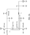
- FIG. 2A illustrates the charging phase ( ⁇ 1) of the inductor L.
- the first switch SW1 is turned on ( ⁇ 1), and the voltage shift component 102 and the inductor L form a voltage divider between the input terminal (VIN) of the buck converter 100 and the output terminal (VA) of the buck converter 100. While a voltage VIN is supplied to a parasitic capacitor C1 at the terminal nc1, a divided voltage (VIN-VA) is supplied to a parasitic capacitor C2 at the terminal nc2.
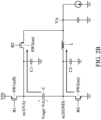
- FIG. 2B illustrates the discharging phase ( ⁇ 2) of the inductor L.
- the second and third switches SW2 and SW3 are turned on ( ⁇ 2), and the current flowing through the inductor L is reduced by the branch current flowing through the turned-on third switch SW3.
- the terminal nc1 (having the parasitic capacitor C1) is at the output voltage VA because of the turned-on third switch SW3.
- the terminal nc2 (having the parasitic capacitor C2) is at the ground voltage GND because of the turned-on second switch SW2.
- the capacitor C is charged to store the voltage (VA-GND) as the voltage shift Vcap required in the charging phase ( ⁇ 1) of the inductor L.
- the voltage swing on the parasitic capacitor C1 is VIN ⁇ VA
- the voltage swing on the parasitic capacitor C2 is (VIN-VA) ⁇ GND.
- the switching loss (CV 2 F) is: C 1 VIN ⁇ VA 2 F + C 2 VIN ⁇ VA ⁇ GND 2 F , which is (C1+C2) (VIN-VA) 2 F.
- (VIN-VA) 2 is usually much lower than VIN 2 .
- the switching loss (CV 2 F) is significantly suppressed.
- VIN-VA 2 is 9, much lower than VIN 2 that is 16.
- the power efficiency of the buck converter 100 is considerably improved by the suppressed switching loss.
- the conduction loss (IR 2 ), it is: IL * D 2 *Rp + IL * 1 ⁇ D 2 * Rn 1 + Ic 2 * Rn 2 + IL 2 * RDC
- IL is the current through the inductor L
- D is the duty cycle of the charging/discharging of the inductor L
- Ic is the current through the capacitor C
- Rp is the parasitic resistor of the first switch SW1 (a PMOS transistor)
- Rn1 is the parasitic resistor of the second switch SW2 (an NMOS transistor)
- Rn2 is the parasitic resistor of the third switch SW3 (another NMOS transistor)
- RDC is the equivalent resistance of the inductor L. Because of the discharging branch design, the current Ic and IL in the last two terms of the conduction loss function are considerably suppressed, and the conduction loss is significantly suppressed.
- the conventional inductor current is divided into the current Ic and the current IL,
- the current Ic and the current IL each may be just half the conventional inductor current.
- the conduction power is recued to (1/2) 2 + (1/2) 2 , half the conventional conduction loss.
- the duty cycle D of the buck converter 100 is discussed in this paragraph.
- the duty cycle D should be set to VA/(VIN-VA).
- a conventional buck converter without the voltage divider design usually operates at a duty cycle VA/VIN.
- the duty cycle of the buck converter 100 is 1/3, which results in a better power efficiency than a conventional buck converter with a duty cycle 1/4.
- the power efficiency of the present invention is obviously much better than conventional buck conversion circuits.
- the output terminal (VA) of the buck converter 100 is directly coupled to the capacitor C through the third switch SW3 during the discharging phase ( ⁇ 2) of the inductor L to charge the capacitor C to store the output voltage VA as the voltage shift Vcap required in the charging phase ( ⁇ 2) of the inductor L.
- the capacitor C may be charged to store another voltage as the voltage shift Vcap.
- FIG. 3 illustrates a buck converter 300 in accordance with another exemplary embodiment of the present invention.
- the buck converter 300 has a voltage shift setting circuit 302, converting the output voltage VA of the buck converter 300 to the expected voltage Ve used in charging the capacitor C during the discharging phase ⁇ 2 of the inductor L.
- b may be 2.
- the voltage shift setting circuit 302 may generate the expected voltage Ve based on the output voltage VA in a non-linear way.
- Any circuit generating the expected voltage Ve based on the output voltage VA may be used to implement the voltage shift setting circuit 302.
- the voltage shift component is implemented by a capacitor C.
- a buck converter can be named a series cap-inductor buck converter.
- the voltage shift component is not limited the single capacitor C illustrated in the figures.
- the proposed buck converter does not add too many switches in its circuit. In comparison with other buck converters using a considerable number of switches, the proposed buck converter using the limited number of switches indeed suppresses the switching loss and does not need a complex circuit design.
Landscapes
- Engineering & Computer Science (AREA)
- Power Engineering (AREA)
- Dc-Dc Converters (AREA)
- Amplifiers (AREA)
- Control Of Motors That Do Not Use Commutators (AREA)
Abstract
Description
- The present invention relates to buck converters.
- A buck converter steps down voltage from an input voltage (supply) to an output voltage (load). It is a class of switched-mode power supply (SMPS), and typically uses an inductor as an energy storage element.
- In a traditional inductor-based buck converter operating at a high conversion rate (e.g., 4V-to-1V), the dominant power loss is the switching loss (CV2F). The high input voltage (e.g., 4V) results in significant switching loss. In addition to the switching loss, the conduction loss (IR2) should also be taken into consideration in the design of a buck converter.
- A buck converter with high power efficiency is called for.
- A buck converter with high power efficiency is proposed.
- In an exemplary embodiment, a buck converter converting an input voltage to an output voltage has an inductor, a voltage shift component, and a discharging branch. The inductor is charged and discharged to regulate the output voltage. The voltage shift component shifts the input voltage to a lower level to charge the inductor. The discharging branch is coupled to the inductor when the inductor is discharged.
- Because of the voltage shift component, the switching loss (CV2F) is significantly suppressed by the lower operating voltages supplied to the parasitic capacitors.
- Because of the discharging branch, the total current on the circuit is suppressed, and the conduction loss (IR2) is significantly suppressed.
- In an exemplary embodiment, the buck converter has a first switch. When being turned on, the first switch couples the input voltage to a first terminal of the voltage shift component. The voltage shift component has a second terminal coupled to the first terminal of the inductor. The inductor has a second terminal coupled to the output terminal of the buck converter that provides the output voltage.
- In an exemplary embodiment, the buck converter has a second switch and a third switch. When being turned on, the second switch couples the first terminal of the inductor to ground. When being turned on, the third switch couples the output terminal of the buck converter to the first terminal of the voltage shift component.
- In an exemplary embodiment, the first switch is turned on in the charging phase of the inductor, and the second switch and the third switch are turned on in the discharging phase of the inductor.
- In an exemplary embodiment, the voltage shift provided by the voltage shift component to lower the input voltage is set during the discharging phase of the inductor.
- In an exemplary embodiment, the voltage shift component is a capacitor.
- In an exemplary embodiment, the output terminal of the buck converter is directly coupled to the capacitor through the third switch during the discharging phase of the inductor.
- In an exemplary embodiment, during the discharging phase of the inductor, the capacitor is charged to store the output voltage as the voltage shift.
- In an exemplary embodiment, the buck converter has a voltage shift setting circuit, converting the output voltage of the buck converter to the expected voltage used in charging the capacitor during the discharging phase of the inductor, for the capacitor to provide the voltage shift during the charging phase of the inductor.
- In an exemplary embodiment, the expected voltage is coupled to the capacitor through the third switch during the discharging phase of the inductor.
- In an exemplary embodiment, the expected voltage is b times the output voltage, where b is a number.
- In an exemplary embodiment, the expected voltage is b times the output voltage plus c, where b and c are two numbers.
- In an exemplary embodiment, the first switch is a p-channel metal oxide semiconductor transistor, and the second switch and the third switch are n-channel metal oxide semiconductor transistors.
- A detailed description is given in the following embodiments with reference to the accompanying drawings.
- The present invention can be more fully understood by reading the subsequent detailed description and examples with references made to the accompanying drawings, wherein:
-
FIG. 1 shows abuck converter 100 in accordance with an exemplary embodiment of the present invention; -
FIG. 2A illustrates the charging phase (Φ1) of the inductor L; -
FIG. 2B illustrates the discharging phase (Φ2) of the inductor L; and -
FIG. 3 illustrates abuck converter 300 in accordance with another exemplary embodiment of the present invention. - The following description is made for the purpose of illustrating the general principles of the invention and should not be taken in a limiting sense. The scope of the invention is best determined by reference to the appended claims.
-
FIG. 1 shows abuck converter 100 in accordance with an exemplary embodiment of the present invention. - The
buck converter 100 converting an input voltage VIN to an output voltage VA has an inductor L, avoltage shift component 102, and adischarging branch 104. The inductor L is charged and discharged to regulate the output voltage VA. Thevoltage shift component 102 shifts the input voltage VIN to a lower level VLX to charge the inductor L. Thedischarging branch 104 is coupled to the inductor L when the inductor L is discharged. - Because of the
voltage shift component 102, the switching loss (CV2F) is significantly suppressed by the lower operating voltages supplied to the parasitic capacitors. InFIG. 1 , thevoltage shift component 102 is a capacitor C, which can be replaced by any component capable of voltage shifting. - Because of the
discharging branch 104, the total current on the circuit is suppressed, and the conduction loss (IR2) is significantly suppressed. - The
voltage shift component 102 also suppresses the voltage ripple of VLX, which is suppressed from VIN to (VIN-VA). Therefore, the inductor current ripple is also suppressed, which further suppresses the inductor ACR loss. - The details of the
buck converter 100 are described in the following paragraphs. - As shown, the
buck converter 100 has a first switch SW1. In thebuck converter 100, the first switch SW1 is a p-channel metal oxide semiconductor (PMOS) transistor but not limited thereto. When being turned on, the first switch SW1 couples the input voltage VIN to a first terminal nC1 of thevoltage shift component 102. Thevoltage shift component 102 has a second terminal nC2 coupled to a first terminal nL1 of the inductor L. The inductor L has a second terminal nL2 that is coupled to the output terminal of thebuck converter 100 that provides the output voltage VA. - The
buck converter 100 has a second switch SW2 and a third switch SW3. In thebuck converter 100, the second switch SW2 and the third switch SW3 are n-channel metal oxide semiconductor (NMOS) transistors but not limited thereto. When being turned on, the second switch SW2 couples the first terminal nL1 of the inductor L to ground (GND). As for the third switch SW3, the turned-on third switch SW3 couples the output terminal (VA) of thebuck converter 100 to the first terminal nC1 of thevoltage shift component 102. - In an exemplary embodiment, the first switch SW1 is turned on in a charging phase Φ1 of the inductor L, and the second switch SW2 and the third switch SW3 are turned on in a discharging phaseΦ2 of the inductor L. In an exemplary embodiment, when the first switch SW1 is turned on in the charging phaseΦ1 of the inductor L, the second and third switches SW2 and SW3 are turned off. When the second and third switches SW2 and SW3 are turned on in the discharging phaseΦ2 of the inductor L, the first switch SW1 is turned off.
- During the discharging phase Φ2 of the inductor L, a voltage shift Vcap provided by the
voltage shift component 102 to lower the input voltage VIN is set. In this example, the voltage shift Vcap is set to VA during the discharging phase Φ2 of the inductor L. -
FIG. 2A illustrates the charging phase (Φ1) of the inductor L. The first switch SW1 is turned on (Φ1), and thevoltage shift component 102 and the inductor L form a voltage divider between the input terminal (VIN) of thebuck converter 100 and the output terminal (VA) of thebuck converter 100. While a voltage VIN is supplied to a parasitic capacitor C1 at the terminal nc1, a divided voltage (VIN-VA) is supplied to a parasitic capacitor C2 at the terminal nc2. -
FIG. 2B illustrates the discharging phase (Φ2) of the inductor L. The second and third switches SW2 and SW3 are turned on (Φ2), and the current flowing through the inductor L is reduced by the branch current flowing through the turned-on third switch SW3. The terminal nc1 (having the parasitic capacitor C1) is at the output voltage VA because of the turned-on third switch SW3. The terminal nc2 (having the parasitic capacitor C2) is at the ground voltage GND because of the turned-on second switch SW2. The capacitor C is charged to store the voltage (VA-GND) as the voltage shift Vcap required in the charging phase (Φ1) of the inductor L. - In this design, the voltage swing on the parasitic capacitor C1 is VIN~VA, and the voltage swing on the parasitic capacitor C2 is (VIN-VA)~GND. The switching loss (CV2F) is:

- For example, when the input voltage VIN is 4V and output voltage VA is IV, (VIN-VA)2 is 9, much lower than VIN2 that is 16. In comparison with the conventional buck converters, the power efficiency of the
buck converter 100 is considerably improved by the suppressed switching loss. - As for the conduction loss (IR2), it is:

- In this design, the conventional inductor current is divided into the current Ic and the current IL, For example, the current Ic and the current IL each may be just half the conventional inductor current. Thus, the conduction power is recued to (1/2)2 + (1/2)2, half the conventional conduction loss.
- Furthermore, the duty cycle D of the
buck converter 100 is discussed in this paragraph. To operate thebuck converter 100, the duty cycle D should be set to VA/(VIN-VA). A conventional buck converter without the voltage divider design usually operates at a duty cycle VA/VIN. For a 4V-to-1V conversion, the duty cycle of thebuck converter 100 is 1/3, which results in a better power efficiency than a conventional buck converter with aduty cycle 1/4. - The power efficiency of the present invention is obviously much better than conventional buck conversion circuits.
- In the forgoing example, the output terminal (VA) of the
buck converter 100 is directly coupled to the capacitor C through the third switch SW3 during the discharging phase (Φ2) of the inductor L to charge the capacitor C to store the output voltage VA as the voltage shift Vcap required in the charging phase (Φ2) of the inductor L. In some other exemplary embodiments, the capacitor C may be charged to store another voltage as the voltage shift Vcap. -
FIG. 3 illustrates abuck converter 300 in accordance with another exemplary embodiment of the present invention. - The
buck converter 300 has a voltageshift setting circuit 302, converting the output voltage VA of thebuck converter 300 to the expected voltage Ve used in charging the capacitor C during the discharging phaseΦ2 of the inductor L. Thus, during the charging phaseΦ1 of the inductor L, the capacitor C provides Ve (=Ve-GND) as the voltage shift Vcap. - In an exemplary embodiment, the expected voltage Ve is b times the output voltage VA, where b is a number. Ve=b∗VA. For example, b may be 2.
- In an exemplary embodiment, the expected voltage Ve is b times the output voltage VA plus c, where b and c are two numbers. Ve=b∗VA + c.
- In another exemplary embodiment, the voltage
shift setting circuit 302 may generate the expected voltage Ve based on the output voltage VA in a non-linear way. - Any circuit generating the expected voltage Ve based on the output voltage VA may be used to implement the voltage
shift setting circuit 302. - In the forgoing exemplary embodiments, the voltage shift component is implemented by a capacitor C. Such a buck converter can be named a series cap-inductor buck converter. However, the voltage shift component is not limited the single capacitor C illustrated in the figures.
- Note that the proposed buck converter does not add too many switches in its circuit. In comparison with other buck converters using a considerable number of switches, the proposed buck converter using the limited number of switches indeed suppresses the switching loss and does not need a complex circuit design.
- While the invention has been described by way of example and in terms of the preferred embodiments, it should be understood that the invention is not limited to the disclosed embodiments. On the contrary, it is intended to cover various modifications and similar arrangements (as would be apparent to those skilled in the art). Therefore, the scope of the appended claims should be accorded the broadest interpretation so as to encompass all such modifications and similar arrangements.
Claims (14)
- A buck converter converting an input voltage to an output voltage, comprising:an inductor, charged and discharged to regulate the output voltage;a voltage shift component, shifting the input voltage to a lower level to charge the inductor; anda discharging branch, coupled to the inductor when the inductor is discharged.
- The buck converter as claimed in claim 1, further comprising:a first switch, coupling the input voltage to a first terminal of the voltage shift component when being turned on;wherein:the voltage shift component has a second terminal coupled to a first terminal of the inductor; andthe inductor has a second terminal coupled to an output terminal of the buck converter that provides the output voltage.
- The buck converter as claimed in claim 2, further comprising:
a second switch, coupling the first terminal of the inductor to ground when being turned on. - The buck converter as claimed in claim 3, further comprising:
a third switch, coupling the output terminal of the buck converter to the first terminal of the voltage shift component when being turned on. - The buck converter as claimed in claim 4, wherein:the first switch is turned on in a charging phase of the inductor; andthe second switch and the third switch are turned on in a discharging phase of the inductor.
- The buck converter as claimed in claim 5, wherein:
a voltage shift provided by the voltage shift component to lower the input voltage is set during the discharging phase of the inductor. - The buck converter as claimed in claim 6, wherein:
the voltage shift component is a capacitor. - The buck converter as claimed in claim 7, wherein:
the output terminal of the buck converter is directly coupled to the capacitor through the third switch during the discharging phase of the inductor. - The buck converter as claimed in claim 7 or 8, wherein:
during the discharging phase of the inductor, the capacitor is charged to store the output voltage as the voltage shift. - The buck converter as claimed in any one of claims 7 to 9, further comprising:
a voltage shift setting circuit, converting the output voltage of the buck converter to an expected voltage used in charging the capacitor during the discharging phase of the inductor, for the capacitor to provide the voltage shift during the charging phase of the inductor. - The buck converter as claimed in claim 10, wherein:
the expected voltage is coupled to the capacitor through the third switch during the discharging phase of the inductor. - The buck converter as claimed in claim 11, wherein:
the expected voltage is b times the output voltage, where b is a number. - The buck converter as claimed in claim 11, wherein:
the expected voltage is b times the output voltage plus c, where b and c are two numbers. - The buck converter as claimed in any one of claims 5 to 13, wherein:the first switch is a p-channel metal oxide semiconductor transistor; andthe second switch and the third switch are n-channel metal oxide semiconductor transistors.
Applications Claiming Priority (2)
| Application Number | Priority Date | Filing Date | Title |
|---|---|---|---|
| US202163282209P | 2021-11-23 | 2021-11-23 | |
| US17/821,215 US12483124B2 (en) | 2021-11-23 | 2022-08-22 | Buck converter with high power efficiency |
Publications (1)
| Publication Number | Publication Date |
|---|---|
| EP4184775A1 true EP4184775A1 (en) | 2023-05-24 |
Family
ID=84361131
Family Applications (1)
| Application Number | Title | Priority Date | Filing Date |
|---|---|---|---|
| EP22208781.9A Pending EP4184775A1 (en) | 2021-11-23 | 2022-11-22 | Buck converter with high power efficiency |
Country Status (4)
| Country | Link |
|---|---|
| US (2) | US12483124B2 (en) |
| EP (1) | EP4184775A1 (en) |
| CN (1) | CN116155097A (en) |
| TW (1) | TWI815668B (en) |
Citations (1)
| Publication number | Priority date | Publication date | Assignee | Title |
|---|---|---|---|---|
| US20210336541A1 (en) * | 2019-01-04 | 2021-10-28 | Huawei Technologies Co., Ltd. | Dc-dc converter |
Family Cites Families (10)
| Publication number | Priority date | Publication date | Assignee | Title |
|---|---|---|---|---|
| US20070229047A1 (en) | 2006-03-31 | 2007-10-04 | James Sigamani | Tapped inductor buck dc-dc converter |
| US9178422B2 (en) | 2013-02-21 | 2015-11-03 | Texas Instruments Incorporated | Resonance-based single inductor output-driven DC-DC converter and method |
| CN104052265B (en) * | 2013-03-15 | 2018-11-06 | 弗莱克斯电子有限责任公司 | Coupling inductor DC decompression converter |
| US10615692B2 (en) | 2014-04-25 | 2020-04-07 | Texas Instruments Incorporated | Series capacitor buck converter having circuitry for precharging the series capacitor |
| TWI568156B (en) | 2014-09-03 | 2017-01-21 | 映興電子股份有限公司 | Step down dc converter |
| US9450491B2 (en) * | 2014-10-23 | 2016-09-20 | Qualcomm Incorporated | Circuits and methods providing three-level signals at a synchronous buck converter |
| US9923465B2 (en) * | 2016-08-16 | 2018-03-20 | Mediatek Inc. | Power conversion circuit and associated operating method |
| TWI659589B (en) | 2018-06-11 | 2019-05-11 | 盈正豫順電子股份有限公司 | High-performed multi-level charging device and method thereof |
| TWI737242B (en) | 2019-03-29 | 2021-08-21 | 美商亮銳公司 | Light emitting device, light emitting system and method of operating a light emitting diode driver |
| US12362666B2 (en) * | 2022-01-13 | 2025-07-15 | Samsung Electronics Co., Ltd. | Semiconductor device |
-
2022
- 2022-08-22 US US17/821,215 patent/US12483124B2/en active Active
- 2022-09-19 TW TW111135333A patent/TWI815668B/en active
- 2022-09-19 CN CN202211140106.2A patent/CN116155097A/en active Pending
- 2022-11-22 EP EP22208781.9A patent/EP4184775A1/en active Pending
-
2025
- 2025-10-28 US US19/371,083 patent/US20260051817A1/en active Pending
Patent Citations (1)
| Publication number | Priority date | Publication date | Assignee | Title |
|---|---|---|---|---|
| US20210336541A1 (en) * | 2019-01-04 | 2021-10-28 | Huawei Technologies Co., Ltd. | Dc-dc converter |
Also Published As
| Publication number | Publication date |
|---|---|
| CN116155097A (en) | 2023-05-23 |
| TWI815668B (en) | 2023-09-11 |
| US20230163685A1 (en) | 2023-05-25 |
| TW202322533A (en) | 2023-06-01 |
| US12483124B2 (en) | 2025-11-25 |
| US20260051817A1 (en) | 2026-02-19 |
Similar Documents
| Publication | Publication Date | Title |
|---|---|---|
| US20260058557A1 (en) | Power converter with capacitive energy transfer and fast dynamic response | |
| US5973944A (en) | Inductorless step-up and step-down converter with inrush current limiting | |
| US10447158B2 (en) | Reducing voltage rating of devices in a multilevel converter | |
| CN110365208B (en) | High efficiency buck-boost charge pump and method therefor | |
| KR101168488B1 (en) | Charge control circuit | |
| KR100516084B1 (en) | Method of controlling dc-dc converter | |
| US8836300B2 (en) | Step-down switching regulator | |
| JP6213268B2 (en) | Power converter | |
| KR20030027729A (en) | Dc-dc converter | |
| EP1356579B1 (en) | A dc/dc up/down converter | |
| US10447161B2 (en) | Inverting buck-boost power converter | |
| EP3893371A1 (en) | Dcdc converter | |
| JP2017147787A (en) | Multi-output dc-dc converter | |
| CN101855817B (en) | Switcing power supply, control circuit controlling switching power supply and control method of switching power supply | |
| US12483124B2 (en) | Buck converter with high power efficiency | |
| US20070018622A1 (en) | Flexible buck converter to generate an output voltage higher or lower than an input voltage | |
| US7586212B2 (en) | Multi-output power supply apparatus | |
| US20230097921A1 (en) | Gate driver circuit for a power supply voltage converter | |
| KR102747752B1 (en) | Hybrid buck converter | |
| JP2005204366A (en) | Dc-dc converter | |
| EP4290748A1 (en) | Voltage regulator with reduced power loss and chip using the voltage regulator | |
| Zhao et al. | A Switched-Capacitor Hybrid Quadratic Buck Converter for 48V-Input Wide-Range Conversion | |
| US10418909B1 (en) | Output switched switching converter | |
| JPH0295165A (en) | Dc/dc converter | |
| Li et al. | A Single-Mode Three-Phase Dual-Path Hybrid Buck-Boost Converter with Extended VCR Range and Always-Reduced Conduction Loss |
Legal Events
| Date | Code | Title | Description |
|---|---|---|---|
| PUAI | Public reference made under article 153(3) epc to a published international application that has entered the european phase |
Free format text: ORIGINAL CODE: 0009012 |
|
| STAA | Information on the status of an ep patent application or granted ep patent |
Free format text: STATUS: THE APPLICATION HAS BEEN PUBLISHED |
|
| AK | Designated contracting states |
Kind code of ref document: A1 Designated state(s): AL AT BE BG CH CY CZ DE DK EE ES FI FR GB GR HR HU IE IS IT LI LT LU LV MC ME MK MT NL NO PL PT RO RS SE SI SK SM TR |
|
| STAA | Information on the status of an ep patent application or granted ep patent |
Free format text: STATUS: REQUEST FOR EXAMINATION WAS MADE |
|
| 17P | Request for examination filed |
Effective date: 20231124 |
|
| RBV | Designated contracting states (corrected) |
Designated state(s): AL AT BE BG CH CY CZ DE DK EE ES FI FR GB GR HR HU IE IS IT LI LT LU LV MC ME MK MT NL NO PL PT RO RS SE SI SK SM TR |
|
| STAA | Information on the status of an ep patent application or granted ep patent |
Free format text: STATUS: EXAMINATION IS IN PROGRESS |
|
| 17Q | First examination report despatched |
Effective date: 20240322 |
|
| GRAP | Despatch of communication of intention to grant a patent |
Free format text: ORIGINAL CODE: EPIDOSNIGR1 |
|
| STAA | Information on the status of an ep patent application or granted ep patent |
Free format text: STATUS: GRANT OF PATENT IS INTENDED |