JP2017147787A - Multi-output dc-dc converter - Google Patents
Multi-output dc-dc converter Download PDFInfo
- Publication number
- JP2017147787A JP2017147787A JP2016026003A JP2016026003A JP2017147787A JP 2017147787 A JP2017147787 A JP 2017147787A JP 2016026003 A JP2016026003 A JP 2016026003A JP 2016026003 A JP2016026003 A JP 2016026003A JP 2017147787 A JP2017147787 A JP 2017147787A
- Authority
- JP
- Japan
- Prior art keywords
- switch
- output
- turned
- inductor
- voltage
- Prior art date
- Legal status (The legal status is an assumption and is not a legal conclusion. Google has not performed a legal analysis and makes no representation as to the accuracy of the status listed.)
- Pending
Links
Images


Classifications
-
- H—ELECTRICITY
- H02—GENERATION; CONVERSION OR DISTRIBUTION OF ELECTRIC POWER
- H02M—APPARATUS FOR CONVERSION BETWEEN AC AND AC, BETWEEN AC AND DC, OR BETWEEN DC AND DC, AND FOR USE WITH MAINS OR SIMILAR POWER SUPPLY SYSTEMS; CONVERSION OF DC OR AC INPUT POWER INTO SURGE OUTPUT POWER; CONTROL OR REGULATION THEREOF
- H02M3/00—Conversion of dc power input into dc power output
- H02M3/02—Conversion of dc power input into dc power output without intermediate conversion into ac
- H02M3/04—Conversion of dc power input into dc power output without intermediate conversion into ac by static converters
- H02M3/10—Conversion of dc power input into dc power output without intermediate conversion into ac by static converters using discharge tubes with control electrode or semiconductor devices with control electrode
- H02M3/145—Conversion of dc power input into dc power output without intermediate conversion into ac by static converters using discharge tubes with control electrode or semiconductor devices with control electrode using devices of a triode or transistor type requiring continuous application of a control signal
- H02M3/155—Conversion of dc power input into dc power output without intermediate conversion into ac by static converters using discharge tubes with control electrode or semiconductor devices with control electrode using devices of a triode or transistor type requiring continuous application of a control signal using semiconductor devices only
- H02M3/156—Conversion of dc power input into dc power output without intermediate conversion into ac by static converters using discharge tubes with control electrode or semiconductor devices with control electrode using devices of a triode or transistor type requiring continuous application of a control signal using semiconductor devices only with automatic control of output voltage or current, e.g. switching regulators
- H02M3/157—Conversion of dc power input into dc power output without intermediate conversion into ac by static converters using discharge tubes with control electrode or semiconductor devices with control electrode using devices of a triode or transistor type requiring continuous application of a control signal using semiconductor devices only with automatic control of output voltage or current, e.g. switching regulators with digital control
-
- H—ELECTRICITY
- H02—GENERATION; CONVERSION OR DISTRIBUTION OF ELECTRIC POWER
- H02M—APPARATUS FOR CONVERSION BETWEEN AC AND AC, BETWEEN AC AND DC, OR BETWEEN DC AND DC, AND FOR USE WITH MAINS OR SIMILAR POWER SUPPLY SYSTEMS; CONVERSION OF DC OR AC INPUT POWER INTO SURGE OUTPUT POWER; CONTROL OR REGULATION THEREOF
- H02M3/00—Conversion of dc power input into dc power output
- H02M3/02—Conversion of dc power input into dc power output without intermediate conversion into ac
- H02M3/04—Conversion of dc power input into dc power output without intermediate conversion into ac by static converters
- H02M3/10—Conversion of dc power input into dc power output without intermediate conversion into ac by static converters using discharge tubes with control electrode or semiconductor devices with control electrode
- H02M3/145—Conversion of dc power input into dc power output without intermediate conversion into ac by static converters using discharge tubes with control electrode or semiconductor devices with control electrode using devices of a triode or transistor type requiring continuous application of a control signal
- H02M3/155—Conversion of dc power input into dc power output without intermediate conversion into ac by static converters using discharge tubes with control electrode or semiconductor devices with control electrode using devices of a triode or transistor type requiring continuous application of a control signal using semiconductor devices only
- H02M3/156—Conversion of dc power input into dc power output without intermediate conversion into ac by static converters using discharge tubes with control electrode or semiconductor devices with control electrode using devices of a triode or transistor type requiring continuous application of a control signal using semiconductor devices only with automatic control of output voltage or current, e.g. switching regulators
- H02M3/158—Conversion of dc power input into dc power output without intermediate conversion into ac by static converters using discharge tubes with control electrode or semiconductor devices with control electrode using devices of a triode or transistor type requiring continuous application of a control signal using semiconductor devices only with automatic control of output voltage or current, e.g. switching regulators including plural semiconductor devices as final control devices for a single load
-
- H—ELECTRICITY
- H02—GENERATION; CONVERSION OR DISTRIBUTION OF ELECTRIC POWER
- H02M—APPARATUS FOR CONVERSION BETWEEN AC AND AC, BETWEEN AC AND DC, OR BETWEEN DC AND DC, AND FOR USE WITH MAINS OR SIMILAR POWER SUPPLY SYSTEMS; CONVERSION OF DC OR AC INPUT POWER INTO SURGE OUTPUT POWER; CONTROL OR REGULATION THEREOF
- H02M1/00—Details of apparatus for conversion
- H02M1/08—Circuits specially adapted for the generation of control voltages for semiconductor devices incorporated in static converters
-
- H—ELECTRICITY
- H02—GENERATION; CONVERSION OR DISTRIBUTION OF ELECTRIC POWER
- H02M—APPARATUS FOR CONVERSION BETWEEN AC AND AC, BETWEEN AC AND DC, OR BETWEEN DC AND DC, AND FOR USE WITH MAINS OR SIMILAR POWER SUPPLY SYSTEMS; CONVERSION OF DC OR AC INPUT POWER INTO SURGE OUTPUT POWER; CONTROL OR REGULATION THEREOF
- H02M1/00—Details of apparatus for conversion
- H02M1/0003—Details of control, feedback or regulation circuits
- H02M1/0009—Devices or circuits for detecting current in a converter
-
- H—ELECTRICITY
- H02—GENERATION; CONVERSION OR DISTRIBUTION OF ELECTRIC POWER
- H02M—APPARATUS FOR CONVERSION BETWEEN AC AND AC, BETWEEN AC AND DC, OR BETWEEN DC AND DC, AND FOR USE WITH MAINS OR SIMILAR POWER SUPPLY SYSTEMS; CONVERSION OF DC OR AC INPUT POWER INTO SURGE OUTPUT POWER; CONTROL OR REGULATION THEREOF
- H02M1/00—Details of apparatus for conversion
- H02M1/0083—Converters characterised by their input or output configuration
- H02M1/009—Converters characterised by their input or output configuration having two or more independently controlled outputs
Abstract
Description
この発明の実施形態は、多出力DC−DCコンバータに関する。 Embodiments described herein relate generally to a multi-output DC-DC converter.
多出力DC−DCコンバータは、既定の順序にて、既定の回数ごとに、複数の出力先に電流を供給する。出力先は、複数の出力先に接続されているスイッチのいずれか1つを所定の周期ごとにオンにするという時分割制御にて、決定される。また、各出力は、外部からの制御信号に基づき、任意のタイミングにて、停止することもできる。但し、制御信号に基づき出力の1つを停止させた場合、停止させた出力が本来出力されている期間においては、いずれの出力先も電流が供給されない。 The multi-output DC-DC converter supplies current to a plurality of output destinations in a predetermined order and every predetermined number of times. The output destination is determined by time division control in which any one of the switches connected to the plurality of output destinations is turned on every predetermined cycle. Each output can be stopped at an arbitrary timing based on an external control signal. However, when one of the outputs is stopped based on the control signal, no current is supplied to any of the output destinations during the period in which the stopped output is originally output.
また、多出力DC−DCコンバータの出力先の1つを、自身が備える制御回路の電源として用いている場合に、その制御回路への出力電力が低下し制御回路が停止すると、回路全体が停止してしまうという問題がある。この問題に対し、制御回路の電源用の出力の電圧が閾値以下になった際に、他のすべての出力を停止する回路を付加するという方法が知られている。しかし、時分割制御においては、各出力に割り当てられた時間配分は変化しないため、必要な出力先への電力供給が開始されるまでに待ち時間が生ずる。ゆえに、制御回路への出力電圧の回復には時間を要する。このように、他の出力を停止させたとしても、優先したい出力先に電力供給が開始されるまでに時間を要し、効率が悪いという問題があった。 In addition, when one of the output destinations of a multi-output DC-DC converter is used as a power supply for a control circuit included in the multi-output DC-DC converter, if the output power to the control circuit decreases and the control circuit stops, the entire circuit stops. There is a problem of end up. In order to solve this problem, there is known a method of adding a circuit for stopping all other outputs when the voltage of the output for the power supply of the control circuit becomes equal to or lower than a threshold value. However, in the time-sharing control, the time distribution assigned to each output does not change, so that a waiting time is generated before the power supply to the required output destination is started. Therefore, it takes time to recover the output voltage to the control circuit. Thus, even if other outputs are stopped, there is a problem that it takes time until the power supply to the output destination to be prioritized is started and the efficiency is poor.
多出力DC−DCコンバータにおいて、優先させる出力先に電力供給が開始されるまでに要する時間を短縮することを目的とする。 In a multi-output DC-DC converter, an object is to shorten the time required until power supply is started to an output destination to be prioritized.
本発明の実施形態としてのDC−DCコンバータは、入力電圧が入力される入力端子と、出力電圧を出力する複数の出力端子と、入力端子に一端が接続されたインダクタと、オンオフ制御されることにより、インダクタに流れる電流を変化させる第1スイッチと、インダクタと、複数の出力端子のうちの1つである第1出力端子との間に一端が接続され、他端がグランドに接続される第1コンデンサと、インダクタと第1コンデンサとの間に接続された第2スイッチと、第1出力端子からの第1出力電圧が予め定められた第1閾値より小さい場合に、第1のスイッチがオフとなったときは、第2スイッチをオンにするよう制御するスイッチ制御部と、を備える。 The DC-DC converter as an embodiment of the present invention is on / off controlled with an input terminal to which an input voltage is input, a plurality of output terminals for outputting the output voltage, an inductor having one end connected to the input terminal, and the like. Accordingly, one end is connected between the first switch that changes the current flowing through the inductor, the inductor, and the first output terminal that is one of the plurality of output terminals, and the other end is connected to the ground. 1 capacitor, a second switch connected between the inductor and the first capacitor, and the first switch is turned off when the first output voltage from the first output terminal is smaller than a predetermined first threshold value. A switch control unit that controls to turn on the second switch.
以下、図面を参照しながら、本発明の実施形態について説明する。 Hereinafter, embodiments of the present invention will be described with reference to the drawings.
(第1の実施形態)
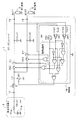
図1は、第1の実施形態に係るDC−DCコンバータを有する回路構成の一例を示す図である。第1の実施形態に係るDC−DCコンバータ1と、熱電発電素子2とからなる熱電発電装置(電源装置)の回路図が示されている。第1の実施形態に係るDC−DCコンバータ1は、入力端子11と、第1出力端子12と、第2出力端子13と、インダクタLと、第1スイッチSW1と、第2スイッチSW2と、第3スイッチSW3と、コンデンサCout1と、2つの電流検知回路ID1およびID2と、制御部14とを備える。
(First embodiment)
FIG. 1 is a diagram illustrating an example of a circuit configuration including a DC-DC converter according to the first embodiment. A circuit diagram of a thermoelectric power generation device (power supply device) including a DC-
制御部14は、発振器OSCと、比較器(コンパレータ)CMP1と、論理回路部141を備える。論理回路部141は、発振器OSCおよび比較器CMP1からの出力を処理し、第1スイッチSW1、第2スイッチSW2、および第3スイッチSW3のスイッチのオンまたはオフの動作(スイッチング)を制御できるものとする。図1では、4つのAND回路(ANDゲート)と、2つのNOT回路(インバータ)とにより、所望のスイッチング制御を実現する。
The
なお、この図で表したDC−DCコンバータ1の構成は一例であり、異なる構成であっても、図示しない構成要素を含んでもよい。例えば、電流検知回路ID1およびID2は、電流の逆流を防ぐために用いられているが、電流の逆流を防ぐ他のものを使用してもよい。その他にも、例えば、制御部14は、第1の実施形態が行うスイッチの制御を実現することができるものであれば、制御部14が備える論理回路部141の構成は、任意に定めてよい。
Note that the configuration of the DC-
熱電発電素子2は、起電力Vteg、出力抵抗Rtegでモデル化された熱電発電装置である。起電力Vtegは、熱電発電素子2を構成する高温側部材と低温側部材との温度差に比例する。例えば、数℃程度の温度差では、一般的に数10mV〜数100mVとなる。また出力抵抗Rtegは、温度に関わらずほぼ一定の値であり、数Ω〜数100Ω程度の値となる。熱電発電素子2の出力電圧Vinは、コンバータ入力容量Cinにより平滑化され、DC−DCコンバータ1の入力電圧Vinともなる。通常の電子回路は1V以上の電源電圧で動作する。そのため一般的に、熱電発電素子と昇圧型DC−DCコンバータとが組み合わされて用いられる。なお、発電素子は起電力が小さければ、熱電発電素子によらずともよい。
The
次に、DC−DCコンバータ1を構成する各部について説明する。
Next, each part which comprises the DC-
DC−DCコンバータ1の入力端子11は、熱電発電素子2に接続され、入力電圧Vinが入力される。第1出力端子12は、第1負荷3に接続され、第1出力電圧Vout1を出力(供給)する。第2出力端子13は、二次電池4に接続され、第2出力電圧Vout2を出力(供給)する。
An
第1出力電圧Vout1および第2出力電圧Vout2は、インダクタL、第1スイッチSW1、第2スイッチSW2、第3スイッチSW3、およびスイッチの開閉を制御する発振器OSCの働きにより、入力電圧Vinよりも高い電圧となる。第1出力電圧Vout1はコンデンサCout1により平滑化され、第1負荷3に対し供給される。第2出力端子13には二次電池4が接続されている。第2出力端子13からの第2出力電圧Vout2により、二次電池4は充電される。
The first output voltage Vout1 and the second output voltage Vout2 are higher than the input voltage Vin due to the action of the inductor L, the first switch SW1, the second switch SW2, the third switch SW3, and the oscillator OSC that controls opening and closing of the switches. Voltage. The first output voltage Vout1 is smoothed by the capacitor Cout1 and supplied to the
このように、第1の実施形態に係るDC−DCコンバータ1は、入力電圧Vinを所定の電圧に変換した上で、負荷および二次電池4などの供給先に出力するものである。なお、図1では、一例として、入力端子11を介して熱電発電素子2と、第1出力端子12を介して第1負荷3と、第2出力端子13を介して二次電池4と接続されていることを想定したが、接続先の構成も限られるものではない。
As described above, the DC-
インダクタLは、一端が入力端子11に接続され、他端(片側端子LX)が第1スイッチSW1、第2スイッチSW2および第3スイッチSW3に接続されている。インダクタLは、第1スイッチSW1、第2スイッチSW2、および第3スイッチSW3の開閉により、入力電圧Vinを第1出力電圧Vout1または第2出力電圧Vout2に変換する。
The inductor L has one end connected to the
電流検知回路ID1およびID2はそれぞれ、第2スイッチSW2および第3スイッチSW3のインダクタLと接続されていない側の他端のそれぞれと接続されている。電流検知回路ID1は、電流の逆流を防止するために、第2スイッチSW2に流れる電流が出力端子側の方向に正の値であればHighを、0以下であればLowを出力する。同様に、電流検知回路ID2は、第3スイッチSW3に流れる電流が出力端子側の方向に正の値であればHighを、0以下であればLowを出力する。 The current detection circuits ID1 and ID2 are connected to the other ends of the second switch SW2 and the third switch SW3 on the side not connected to the inductor L, respectively. The current detection circuit ID1 outputs High if the current flowing through the second switch SW2 is a positive value in the direction toward the output terminal, and outputs Low if the current is less than 0, in order to prevent reverse current flow. Similarly, the current detection circuit ID2 outputs High if the current flowing through the third switch SW3 is a positive value in the direction toward the output terminal, and outputs Low if the current is 0 or less.
コンデンサCout1は、電流検知回路ID1の、第2スイッチSW2に接続されていない方の他端に接続され、第1出力電圧Vout1を平滑化して、第1負荷3に供給する。
The capacitor Cout1 is connected to the other end of the current detection circuit ID1 that is not connected to the second switch SW2, and smoothes the first output voltage Vout1 and supplies it to the
制御部14は、第1スイッチSW1、第2スイッチSW2、および第3スイッチSW3のスイッチングを制御する。制御部14の比較器CMP1は、第1出力電圧Vout1と、制御部内部からの第1参照電圧Vref1とを比較する。これは、第1参照電圧Vref1を基準値として、第1出力電圧Vout1と所定の基準値との大小関係に基づき、出力先を切り替えるためである。図1の例では、比較器CMP1からの出力信号を2つに分岐し、一方をインバータにより反転させる。これにより、所定の条件下において、第2スイッチSW2と第3スイッチSW3の一方がオンで、他方がオフである状況を作り出す。
The
制御部14の発振器OSCは、各スイッチのスイッチングをするタイミングを制御するためのものである。以下に、各スイッチのスイッチングの制御について説明する。
The oscillator OSC of the
第1スイッチSW1は、発振器OSCに基づき、オンまたはオフの状態が決定される。発振器OSCの出力がHighのときはオン、Lowのときはオフになる。なお、発振器OSCの出力がHighを出力している期間とLowを出力している期間の長さは、同じでも異なっていてもよい。 The first switch SW1 is turned on or off based on the oscillator OSC. When the output of the oscillator OSC is high, it is on, and when it is low, it is off. Note that the length of the period during which the output of the oscillator OSC outputs High and the period during which Low is output may be the same or different.
第2スイッチSW2は、発振器OSCと比較器CMP1と電流検知回路ID1に基づき、オンまたはオフの状態が決定される。発振器OSCの出力がHighのときはオフになる。一方、発振器OSCの出力がLowであっても、比較器CMP1の出力がHigh(Vref1>Vout1)でなければ、オンにならない。また、電流検知回路ID1がLow、つまり第1出力端子12側から入力端子11側の方向に電流が流れようとするとオフになる。
The second switch SW2 is turned on or off based on the oscillator OSC, the comparator CMP1, and the current detection circuit ID1. It turns off when the output of the oscillator OSC is High. On the other hand, even if the output of the oscillator OSC is Low, the output is not turned on unless the output of the comparator CMP1 is High (Vref1> Vout1). Further, when the current detection circuit ID1 is Low, that is, when the current is about to flow from the
第3スイッチSW3は、発振器OSCと比較器CMP1と電流検知回路ID2に基づき、オンまたはオフの状態が決定される。発振器OSCの出力がHighのときは必ずオフになる。発振器OSCの出力がLowであっても、比較器CMP1の出力がLow(Vref1<Vout1)でなければ、オンにならない。また、電流検知回路ID2がLow、つまり第2出力端子13側から入力端子11側の方向に電流が流れようとするとオフになる。
The third switch SW3 is turned on or off based on the oscillator OSC, the comparator CMP1, and the current detection circuit ID2. It is always off when the output of the oscillator OSC is High. Even if the output of the oscillator OSC is Low, the output is not turned on unless the output of the comparator CMP1 is Low (Vref1 <Vout1). Further, when the current detection circuit ID2 is Low, that is, when the current is about to flow from the
図2は、第1の実施形態における各スイッチのスイッチングの制御を説明する図である。図2には、発振器OSCの出力信号と第1スイッチSW1の状態、インダクタ電流IL、第1出力電圧Vout1、第2スイッチSW2の状態、および第3スイッチSW3の状態が示されている。第1スイッチSW1、第2スイッチSW2、および第3スイッチSW3の状態は、オンが1、オフが0にて示されている。 FIG. 2 is a diagram for explaining the switching control of each switch in the first embodiment. FIG. 2 shows the output signal of the oscillator OSC, the state of the first switch SW1, the inductor current IL, the first output voltage Vout1, the state of the second switch SW2, and the state of the third switch SW3. The states of the first switch SW1, the second switch SW2, and the third switch SW3 are indicated as 1 for on and 0 for off.
第1スイッチSW1のスイッチングは、発振器OSCに基づき決定されるため、第1スイッチSW1の状態と発振器OSCの出力信号の波形は同じであり、一番上の波形にて合わせて示されている。 Since the switching of the first switch SW1 is determined based on the oscillator OSC, the state of the first switch SW1 and the waveform of the output signal of the oscillator OSC are the same and are shown together in the top waveform.
発振器OSCの出力がHighを出力している間は、第1スイッチSW1がオン、第2スイッチSW2と第3スイッチSW3はともにオフとなる。ゆえに、この期間内において、上から2番目の波形に示すように、インダクタ電流ILは増加していく。一方、第2スイッチSW2がオフであることから、この期間内において、上から3番目の波形に示すように、第1出力電圧Vout1は減少していく。ここで、時刻t1に、第1出力電圧Vout1が第1参照電圧Vref1を下回るとする。そうすると、時刻t1の後、比較器CMP1の出力はLowからHighへと切り替わる。なお、比較器CMP1が入力を受け付けてから出力を切り替えるまでには、タイムラグがあるものとする。 While the output of the oscillator OSC is high, the first switch SW1 is turned on, and the second switch SW2 and the third switch SW3 are both turned off. Therefore, in this period, the inductor current IL increases as shown in the second waveform from the top. On the other hand, since the second switch SW2 is off, the first output voltage Vout1 decreases during this period as shown by the third waveform from the top. Here, it is assumed that the first output voltage Vout1 falls below the first reference voltage Vref1 at time t1. Then, after time t1, the output of the comparator CMP1 switches from Low to High. It is assumed that there is a time lag between the time when the comparator CMP1 receives an input and the time when the output is switched.
そして、時刻t1の後の時刻t2にて、発振器OSCの出力がLowを出力するようになると、第1スイッチSW1がオフとなり、また比較器CMP1の出力がHighであることから、第2スイッチSW2がオンとなる。また、第3スイッチSW3はオフのままである。これにより、インダクタ電流ILが第1負荷3に流れ込み、Vout1は増加する。一方、インダクタ電流ILは逆に下降していき、電流が流れなくなると、電流検知回路ID1の出力がLowに切り替わる。ゆえに、第2スイッチSW2がオフとなるため、第1出力端子12側からの電流がインダクタLに流れることは防がれる。
When the output of the oscillator OSC outputs Low at time t2 after time t1, the first switch SW1 is turned off, and the output of the comparator CMP1 is High, so the second switch SW2 Is turned on. Further, the third switch SW3 remains off. As a result, the inductor current IL flows into the
なお、時刻t3に第1出力電圧Vout1が第1参照電圧Vref1を上回るとする。第1出力電圧Vout1が第1参照電圧Vref1を上回ると、比較器CMP1の出力はLowへ切り替わる。但し、第1出力電圧Vout1が第1参照電圧Vref1を上回る時刻と、比較器CMP1の出力がLowへ切り替わる時刻とにはタイムラグがある。このタイムラグを調整し、比較器CMP1の出力がLowへ切り替わる前に、インダクタ電流ILが0(ゼロ)になるようにする。このインダクタ電流ILが流れなくなる時刻t4において、第2スイッチSW2はオフになる。 It is assumed that the first output voltage Vout1 exceeds the first reference voltage Vref1 at time t3. When the first output voltage Vout1 exceeds the first reference voltage Vref1, the output of the comparator CMP1 switches to Low. However, there is a time lag between the time when the first output voltage Vout1 exceeds the first reference voltage Vref1 and the time when the output of the comparator CMP1 switches to Low. This time lag is adjusted so that the inductor current IL becomes 0 (zero) before the output of the comparator CMP1 switches to Low. At time t4 when the inductor current IL does not flow, the second switch SW2 is turned off.
時刻t4の後、時刻t5に発振器OSCの出力がHighとなると、第1スイッチSW1がオンとなり、第2スイッチSW2および第3スイッチSW3はオフのままであるため、インダクタ電流ILは上昇する。そして、次に第1スイッチSW1がオフされる時刻t6においては、まだ第1出力電圧Vout1は第1参照電圧Vref1よりも高いものとする。そうすると、比較器CMP1の出力がLowのままであるから、時刻t6において第2スイッチSW2ではなく、第3スイッチSW3がオンとなる。ゆえに、インダクタ電流ILが第2出力端子13に流れこみ、二次電池4が充電される。やがてインダクタ電流ILが下降し流れなくなると、電流検知回路ID2の出力がLowへ切り替わる。そうすると、第3スイッチSW3がオフとなるため、第2出力端子13側からの電流がインダクタLに流れることは防がれる。
After time t4, when the output of the oscillator OSC becomes High at time t5, the first switch SW1 is turned on and the second switch SW2 and the third switch SW3 remain off, so that the inductor current IL increases. Then, at the time t6 when the first switch SW1 is turned off next, the first output voltage Vout1 is still higher than the first reference voltage Vref1. Then, since the output of the comparator CMP1 remains Low, the third switch SW3 is turned on instead of the second switch SW2 at time t6. Therefore, the inductor current IL flows into the
時刻t4の後、第1出力電圧Vout1は、第1負荷3に電流が流れることにより、下降していくが、第1出力電圧Vout1が第1参照電圧Vref1を下回るまでは、第2スイッチSW2はオンとならず、第3スイッチSW3のスイッチングと第1スイッチSW1のスイッチングとが繰り返されていく。そして、再度第1出力電圧Vout1が第1参照電圧Vref1を下回った時刻t7の後、第1スイッチSW1がオフとなる時刻t8に第2スイッチSW2がオンになる。
After time t4, the first output voltage Vout1 decreases due to the current flowing through the
なお、図2では、時刻t6において、第1出力電圧Vout1が第1参照電圧Vref1を超えているため、時刻t6においては、第2スイッチSW2はオンにならずに、第3スイッチSW3がオンとなった。しかし、第1出力電圧Vout1の増加率が小さいなどにより、時刻t6において、第1出力電圧Vout1が第1参照電圧Vref1を超えていないときは、再び第2スイッチSW2がオンとなる場合もあり得る。このように第1出力電圧Vout1と第1参照電圧Vref1の大小関係に基づいて、第2スイッチSW2および第3スイッチSW3のオンオフが決定される。 In FIG. 2, since the first output voltage Vout1 exceeds the first reference voltage Vref1 at time t6, the second switch SW2 is not turned on and the third switch SW3 is turned on at time t6. became. However, the second switch SW2 may be turned on again when the first output voltage Vout1 does not exceed the first reference voltage Vref1 at time t6 due to a small increase rate of the first output voltage Vout1. . Thus, on / off of the second switch SW2 and the third switch SW3 is determined based on the magnitude relationship between the first output voltage Vout1 and the first reference voltage Vref1.
以上のように、第1の実施形態は、複数の出力先のうちの1つの電圧が低下し、閾値である参照電圧以下になると、その出力先のためのスイッチをオンにし、他の出力先のためのスイッチをすべてオフにする制御を行う。これにより、予め定められた時間配分で出力先を制御するのではなく、基準電圧との比較結果に基づき出力先を決定することができる。そのため、既定の順序で出力先を決定する場合に存在していた待ち時間なしで、出力電圧が低下した場合に対応できる。また、優先すべき出力が低下した場合に、出力が閾値を超えるまで、他の出力先に出力せずに、優先すべき出力先に出力することができる。 As described above, in the first embodiment, when the voltage of one of the plurality of output destinations decreases and becomes equal to or lower than the threshold reference voltage, the switch for the output destination is turned on, and the other output destinations. Control to turn off all the switches for. Accordingly, the output destination can be determined based on the comparison result with the reference voltage, instead of controlling the output destination with a predetermined time distribution. Therefore, it is possible to cope with the case where the output voltage is reduced without the waiting time that existed when the output destination is determined in a predetermined order. Further, when the output to be prioritized decreases, it can be output to the output destination to be prioritized without outputting to another output destination until the output exceeds the threshold.
(第2の実施形態)
図3は、第2の実施形態に係るDC−DCコンバータを有する回路構成の一例を示す図である。第2の実施形態では、第1の実施形態における制御部14と、第2出力端子13に関連する部分が、第1の実施形態と異なる。第1の実施形態と同様な点は、説明を省略する。
(Second Embodiment)
FIG. 3 is a diagram illustrating an example of a circuit configuration including the DC-DC converter according to the second embodiment. In 2nd Embodiment, the part relevant to the
第2の実施形態の第2出力端子13に接続されているのは、二次電池4ではなく、第2負荷5とする。また、電流検知回路ID2と第2出力端子13の間に第2コンデンサCout2を設置し、第2出力端子13に係る第2出力電圧Vout2の平滑化を図るものとする。
What is connected to the
第2の実施形態の制御部14は、比較器CMP2をさらに備える。比較器CMP2は、第2出力電圧Vout2と第2参照電圧Vref2を比較し、Vref2>Vout2のときはHighを、Vref2<Vout2のときはLowを出力する。これにより、第1出力電圧Vout1だけでなくVout2も監視することができる。なお、第1参照電圧Vref1と第2参照電圧Vref2とは、出力先である第1負荷3と第2負荷5に与えようとする電圧値により定まる。
The
制御部14は、比較器CMP1とCMP2がともにLowを出力するとき(Vref1<Vout1かつVref2<Vout2)、発振器OSCの出力が第1スイッチSW1に入力されないように構成されている。図3では、比較器CMP1とCMP2がともにLowのときだけLowを出力するOR回路と、OR回路の出力がLowのときには、発振器OSCの出力によらずにLowを出力するAND回路により、上記構成を実現している。なお、本実施形態は、図3の構成に限られるものではない。
The
このように、第1出力電圧Vout1と第2出力電圧Vout2とが大きいときは、第1スイッチSW1のスイッチングを停止させることにより、消費電力を削減することができる。また、第2スイッチSW2と第3スイッチSW3がともにオフの場合において、第1スイッチSW1のスイッチングが行われると、インダクタ電流の流れ先がないことにより、インダクタLの片側端子LXが高電圧になる。しかし、本実施形態では、第2スイッチSW2と第3スイッチSW3がともにオフの場合においては、第1スイッチSW1がスイッチングしないようにし、片側端子LXが高電圧になることを防ぐことができる。 Thus, when the first output voltage Vout1 and the second output voltage Vout2 are large, the power consumption can be reduced by stopping the switching of the first switch SW1. In addition, when both the second switch SW2 and the third switch SW3 are off, when the switching of the first switch SW1 is performed, the one-side terminal LX of the inductor L becomes a high voltage because there is no flow destination of the inductor current. . However, in the present embodiment, when both the second switch SW2 and the third switch SW3 are off, the first switch SW1 can be prevented from switching, and the one-side terminal LX can be prevented from becoming a high voltage.
また、第2の実施形態では、制御部14の電源に、第1出力電圧Vout1を用いるものとする。また、この場合、第1出力電圧Vout1を第2出力電圧Vout2よりも小さくするように(Vout1<Vout2)制御すると、制御部14にて消費される電力を抑えることができ、DC−DCコンバータ1の効率を向上させることができる。Vout1<Vout2となるようにするには、例えば、第1参照電圧Vref1を第2参照電圧Vref2よりも小さく設定すればよい。
In the second embodiment, the first output voltage Vout1 is used as the power source of the
次に、各スイッチのスイッチングの制御について説明する。 Next, switching control of each switch will be described.
第1スイッチSW1は、第1の実施形態と異なり、発振器OSCのみならず、発振器OSC、比較器CMP1、および比較器CMP2に基づき、オンまたはオフの状態が決定される。発振器OSCの出力がLowのとき、第1スイッチSW1はオフになるが、発振器OSCの出力がHighのときでも、オンになるとは限らない。発振器OSCの出力がHighであり、かつ比較器CMP1またはCMP2の出力がHighのとき、第1スイッチSW1はオンになる。 Unlike the first embodiment, the first switch SW1 is turned on or off based not only on the oscillator OSC but also on the oscillator OSC, the comparator CMP1, and the comparator CMP2. When the output of the oscillator OSC is Low, the first switch SW1 is turned off. However, even when the output of the oscillator OSC is High, the first switch SW1 is not always turned on. When the output of the oscillator OSC is High and the output of the comparator CMP1 or CMP2 is High, the first switch SW1 is turned on.
第2スイッチSW2は、第1の実施形態と同じく、発振器OSCと比較器CMP1と電流検知回路ID1に基づき、オンまたはオフの状態が決定される。発振器OSCの出力がHighのときは必ずオフになる。発振器OSCの出力がLowであっても、比較器CMP1の出力がLow(Vref1<Vout1)ならば、オンにならない。また、電流検知回路ID1がLow、つまり第1出力端子12側から入力端子11側の方向に電流が流れようとするときもオフになる。
As in the first embodiment, the second switch SW2 is turned on or off based on the oscillator OSC, the comparator CMP1, and the current detection circuit ID1. It is always off when the output of the oscillator OSC is High. Even if the output of the oscillator OSC is Low, if the output of the comparator CMP1 is Low (Vref1 <Vout1), it does not turn on. It is also turned off when the current detection circuit ID1 is Low, that is, when a current is about to flow from the
第3スイッチSW3は、第1の実施形態と異なり、発振器OSCと比較器CMP1とCMP2と電流検知回路ID2に基づき、オンまたはオフの状態が決定される。発振器OSCの出力がHighのときはオフになる。発振器OSCの出力がLowであっても、比較器CMP1の出力がLow(Vref1<Vout1)かつCMP2の出力がHigh(Vref2>Vout2)でなければ、オンにならない。つまり、ここでは第2スイッチSW2が第3スイッチSW3よりも優先されている。また、電流検知回路ID2がLow、つまり第2出力端子13側から入力端子11側の方向に電流が流れようとするとオフになる。
Unlike the first embodiment, the third switch SW3 is turned on or off based on the oscillator OSC, the comparators CMP1 and CMP2, and the current detection circuit ID2. It turns off when the output of the oscillator OSC is High. Even if the output of the oscillator OSC is Low, the output is not turned on unless the output of the comparator CMP1 is Low (Vref1 <Vout1) and the output of CMP2 is High (Vref2> Vout2). That is, here, the second switch SW2 has priority over the third switch SW3. Further, when the current detection circuit ID2 is Low, that is, when the current is about to flow from the
図4は、第2の実施形態に係る各スイッチのスイッチングの制御を説明する図である。図4には、発振器OSCの出力信号、第1スイッチSW1の状態、インダクタ電流IL、第1出力電圧Vout1、第2出力電圧Vout2、第2スイッチSW2の状態、および第3スイッチSW3の状態の波形が示されている。 FIG. 4 is a diagram illustrating switching control of each switch according to the second embodiment. FIG. 4 shows waveforms of the output signal of the oscillator OSC, the state of the first switch SW1, the inductor current IL, the first output voltage Vout1, the second output voltage Vout2, the state of the second switch SW2, and the state of the third switch SW3. It is shown.
図4で示すように、時刻t1において、第1出力電圧Vout1はVref1を下回るとする。その後の時刻t2までは、比較器CMP1の出力はHighであって、比較器CMP1およびCMP2の出力がともにLowではないため、第1スイッチSW1に発振器OSCの出力が入力されることにより、第1スイッチSW1はオンである。そして、第1の実施形態と同様、第1スイッチSW1がオンの間、インダクタ電流ILが増加する。 As shown in FIG. 4, it is assumed that the first output voltage Vout1 falls below Vref1 at time t1. Until the subsequent time t2, since the output of the comparator CMP1 is High and the outputs of the comparators CMP1 and CMP2 are not Low, the output of the oscillator OSC is input to the first switch SW1, whereby the first The switch SW1 is on. As in the first embodiment, the inductor current IL increases while the first switch SW1 is on.
時刻t2にて発振器OSCの出力がLowに反転した後、第1スイッチSW1はオフになる。また、比較器CMP1の出力がHighのため、第2スイッチSW2はオンになる。したがって、第1の実施形態同様、インダクタ電流ILは次第に下降する。一方、第1出力電圧Vout1は上昇する。 After the output of the oscillator OSC is inverted to Low at time t2, the first switch SW1 is turned off. Further, since the output of the comparator CMP1 is High, the second switch SW2 is turned on. Therefore, like the first embodiment, the inductor current IL gradually decreases. On the other hand, the first output voltage Vout1 increases.
また、第1の実施形態同様、時刻t3にてVout1>Vref1となっても、比較器CMP1の出力はHighからLowへすぐに切り替わらず、インダクタ電流ILが0(ゼロ)になる時刻t4において、第2スイッチSW2はオフになる。 Similarly to the first embodiment, even when Vout1> Vref1 at time t3, the output of the comparator CMP1 does not immediately switch from High to Low, and at time t4 when the inductor current IL becomes 0 (zero). The second switch SW2 is turned off.
また、図4で示すように、時刻t4の後も、Vout2<Vref2とする。そうすると、CMP2の出力はHighであるため、発振器OSCの出力が第1スイッチSW1へと入力されることにより、発振器OSCの出力がHighとなる時刻t5において、第1スイッチSW1はオンとなる。そして、発振器OSCの出力がLowに反転した時刻t6において、第3スイッチSW3の入力がHighとなり、第3スイッチSW3がオンとなる。インダクタ電流ILは、第3スイッチSW3を介して、第2出力端子13へと流れ、Vout2が上昇する。やがてインダクタ電流ILが下降していき0となると電流検知回路ID2の出力がLowへ切り替わり、第3スイッチSW3がオフになる。
Also, as shown in FIG. 4, Vout2 <Vref2 is satisfied even after time t4. Then, since the output of CMP2 is High, when the output of the oscillator OSC is input to the first switch SW1, the first switch SW1 is turned on at time t5 when the output of the oscillator OSC becomes High. At time t6 when the output of the oscillator OSC is inverted to Low, the input of the third switch SW3 becomes High, and the third switch SW3 is turned on. The inductor current IL flows to the
図4のように、1度目の第3スイッチSW3のオンによっても、Vout2が第2参照電圧Vref2を超えず、かつ第1出力電圧Vout1がVref1であるときは、再び発振器OSCの出力がLowとなる時刻t7においても、第3スイッチSW3がオンとなる。このように、第3スイッチSW3のスイッチング、つまり第2負荷5への出力が繰り替えされることもあり得る。なお、第2負荷5への出力を繰り返す間、第2スイッチSW2はオンとならずに電力が供給されないことから、第1出力電圧Vout1は下降し続ける。 As shown in FIG. 4, even when the third switch SW3 is turned on for the first time, when Vout2 does not exceed the second reference voltage Vref2 and the first output voltage Vout1 is Vref1, the output of the oscillator OSC becomes Low again. At time t7, the third switch SW3 is turned on. In this way, the switching of the third switch SW3, that is, the output to the second load 5 may be repeated. Note that while the output to the second load 5 is repeated, the second switch SW2 is not turned on and power is not supplied, so the first output voltage Vout1 continues to decrease.
第1出力電圧Vout1の低下により、時刻t8に再びVout1<Vref1となったときは、CMP2の出力がHighへと切り替わり、発振器OSCの出力がLowとなる時刻t9において、第2スイッチSW2が優先的にオンとなる。このとき、第3スイッチSW3は、Vout2と第2参照電圧Vref2の関係に関わらず、オフである。 When Vout1 <Vref1 again at time t8 due to the decrease in the first output voltage Vout1, the output of CMP2 is switched to High, and at time t9 when the output of the oscillator OSC becomes Low, the second switch SW2 has priority. Turned on. At this time, the third switch SW3 is off regardless of the relationship between Vout2 and the second reference voltage Vref2.
時刻t9における第2スイッチSW2のオンにより、Vout1がVref1を上回ったため、次に発振器OSCがHighを出力する時刻t10では、第3スイッチSW3がオンになる。そして、発振器OSCがHighを出力するさらに次のタイミングである時刻t11では、Vout1>Vref1かつVout2>Vref2であるため、比較器CMP1およびCMP2はともにLowを出力する。したがって、時刻t11では、第1スイッチSW1はオンとはならず、全てのスイッチがオフとなる。また、このスイッチングの停止は、Vout1<Vref1、またはVout2<Vref2となるまで続く。 Since the second switch SW2 is turned on at time t9 and Vout1 exceeds Vref1, the third switch SW3 is turned on at time t10 when the oscillator OSC next outputs High. At time t11, which is the next timing when the oscillator OSC outputs High, since Vout1> Vref1 and Vout2> Vref2, both the comparators CMP1 and CMP2 output Low. Therefore, at time t11, the first switch SW1 is not turned on, and all the switches are turned off. Further, the switching stop is continued until Vout1 <Vref1 or Vout2 <Vref2.
以上のように、第2の実施形態では、出力の1つをコンバータ自身の制御回路の電源として用いる。そして、電源とする電圧がある閾値以下となった場合、その出力が経由するスイッチをオンにし、出力が経由する他の全てのスイッチをオフにし、制御回路用の電源に対して優先的に出力する。これにより、制御部14の電源電圧が低下しても優先して回復させることができ、DC−DCコンバータ1が停止しにくくなり、安定して動作させることができる。また第1出力電圧Vout1を第2出力電圧Vout2よりも低く設定することで、制御部14の消費電力を削減することができ、DC−DCコンバータ1の効率を向上させることができる。
As described above, in the second embodiment, one of the outputs is used as a power source for the control circuit of the converter itself. When the power supply voltage falls below a certain threshold, the switch through which the output passes is turned on, all other switches through which the output passes are turned off, and the output is preferentially given to the power supply for the control circuit. To do. Thereby, even if the power supply voltage of the
(第3の実施形態)
図5は、第3の実施形態に係るDC−DCコンバータを有する回路構成の一例を示す図である。第1の実施形態との相違点を説明し、同様な点は説明を省略する。
(Third embodiment)
FIG. 5 is a diagram illustrating an example of a circuit configuration including a DC-DC converter according to the third embodiment. Differences from the first embodiment will be described, and description of similar points will be omitted.
第3の実施形態の第2スイッチSW2は、ダイオードD2とサブスイッチSubSW2にて構成される。また、第3スイッチSW3は、ダイオードD3とサブスイッチSubSW3にて構成される。 The second switch SW2 of the third embodiment includes a diode D2 and a sub switch SubSW2. The third switch SW3 includes a diode D3 and a sub switch SubSW3.
第2スイッチSW2と第3スイッチSW3に対する制御信号も第1の実施形態と異なる。第3の実施形態における制御部14は、発振器OSCの信号を合成せずに、比較器CMP1の比較結果をSubSW2に出力する。また、比較器CMP1の比較結果を反転して、サブスイッチSubSW3に出力する。ゆえに、これまでの実施形態では、第1スイッチSW1がオンの間は、他のスイッチはスイッチングされずにいたが、第3の実施形態では、第1スイッチSW1がオンの間でも、比較器CMP1の出力が切り替わった時点で、他のスイッチはスイッチングする。
Control signals for the second switch SW2 and the third switch SW3 are also different from those in the first embodiment. The
また、第2スイッチSW2と第3スイッチSW3に接続されていた電流検知回路ID1とID2は、第3の実施形態は備えられていない。 Further, the current detection circuits ID1 and ID2 connected to the second switch SW2 and the third switch SW3 are not provided in the third embodiment.
図6は、第3の実施形態に係る各スイッチのスイッチングの制御を説明する図である。図6には、発振器OSCの出力信号と第1スイッチSW1の状態、インダクタ電流IL、第1出力電圧Vout1、サブスイッチSubSW2、およびサブスイッチSubSW3の状態の波形が示されている。 FIG. 6 is a diagram for explaining switching control of each switch according to the third embodiment. FIG. 6 shows waveforms of the output signal of the oscillator OSC, the state of the first switch SW1, the inductor current IL, the first output voltage Vout1, the sub switch SubSW2, and the state of the sub switch SubSW3.
発振器OSCの出力がHighのときは第1スイッチSW1がオンであり、インダクタ電流ILは上昇していくが、Vout1は下降していく。時刻t1に第1出力電圧Vout1がVref1を下回ると、その後、比較器CMP1の出力はLowからHighへと切り替わり、サブスイッチSubSW2はオン、サブスイッチSubSW3はオフとなる。 When the output of the oscillator OSC is High, the first switch SW1 is on, and the inductor current IL increases, but Vout1 decreases. When the first output voltage Vout1 falls below Vref1 at time t1, the output of the comparator CMP1 is switched from Low to High, and the sub switch SubSW2 is turned on and the sub switch SubSW3 is turned off.
このとき、第1スイッチSW1はオンであるが、ダイオードD2の逆バイアスとなるため、インダクタ電流ILはそのまま上昇を続ける。 At this time, the first switch SW1 is on, but the diode D2 is reverse-biased, so the inductor current IL continues to rise.
時刻t2に発振器OSCの出力がLowに切り替わると第1スイッチSW1がオフし、インダクタLの端子LXの電圧は、第2スイッチSW2のダイオードD2が導通するまで上昇する。ダイオードD2が順バイアスになると、インダクタ電流ILはダイオードD2とサブスイッチSubSW2を通り、第1出力電圧Vout1が上昇していく。このとき、インダクタ電流ILは下降していくが、ダイオードD2により、入力端子11側へと電流が流れることはない。
When the output of the oscillator OSC switches to Low at time t2, the first switch SW1 is turned off, and the voltage at the terminal LX of the inductor L increases until the diode D2 of the second switch SW2 becomes conductive. When the diode D2 becomes forward biased, the inductor current IL passes through the diode D2 and the sub switch SubSW2, and the first output voltage Vout1 increases. At this time, the inductor current IL decreases, but no current flows to the
時刻t3に第1出力電圧Vout1が第1参照電圧Vref1を上回ると、比較器CMP1の出力はLowへ切り替わり、サブスイッチSubSW2はオフ、サブスイッチSubSW3はオンとなる。但し、比較器CMP1のタイムラグにより、時刻t4にサブスイッチSubSW2とサブスイッチSubSW3は、スイッチングするとする。時刻t4の後、第1出力電圧Vout1は徐々に下降する。 When the first output voltage Vout1 exceeds the first reference voltage Vref1 at time t3, the output of the comparator CMP1 is switched to Low, the sub switch SubSW2 is turned off, and the sub switch SubSW3 is turned on. However, it is assumed that the sub-switch SubSW2 and the sub-switch SubSW3 are switched at time t4 due to the time lag of the comparator CMP1. After time t4, the first output voltage Vout1 gradually decreases.
その後の時刻t5において、発振器OSCの出力がHighに切り替わると、インダクタ電流ILは上昇していく。その後の時刻t6において、発振器OSCの出力がLowに切り替わると、第1スイッチSW1がオフになり、端子LXの電圧は、第3スイッチSW3のダイオードD3が導通するまで上昇していく。ダイオードD3が順バイアスになると、インダクタ電流ILはダイオードD3とサブスイッチSubSW3を通り、第2出力端子13に接続された二次電池4が充電される。このとき、インダクタ電流ILは下降していくが、ダイオードD3により、入力端子11側へと電流が流れることはない。
At time t5 thereafter, when the output of the oscillator OSC switches to High, the inductor current IL increases. Thereafter, when the output of the oscillator OSC switches to Low at time t6, the first switch SW1 is turned off, and the voltage at the terminal LX increases until the diode D3 of the third switch SW3 becomes conductive. When the diode D3 becomes forward biased, the inductor current IL passes through the diode D3 and the sub switch SubSW3, and the secondary battery 4 connected to the
第1出力電圧Vout1が第1参照電圧Vref1を下回るまで、第2出力端子13に接続された二次電池4の充電が繰り返し行われる。また、第2スイッチSW2はオンとならずに電力が供給されないことから、第1出力電圧Vout1は下降し続ける。時刻t7に再度第1出力電圧Vout1が第1参照電圧Vref1を下回ると、サブスイッチSubSW2はオン、サブスイッチSubSW3はオフとなり、その後、第1出力電圧Vout1が上昇する。
The secondary battery 4 connected to the
これまでの実施形態では、電流の逆流を防ぐために、インダクタ電流ILに基づき、第2スイッチSW2または第3スイッチSW3をオフしなければならなかった。しかし、本実施形態では、図6に示すように、出力先を切り替えない限り、オフにする必要はない。 In the previous embodiments, the second switch SW2 or the third switch SW3 had to be turned off based on the inductor current IL in order to prevent the backflow of the current. However, in this embodiment, as shown in FIG. 6, it is not necessary to turn it off unless the output destination is switched.
以上のように、第3の実施形態では、ダイオートを用いることにより、第2スイッチSW2および第3スイッチSW3への電流の逆流を防ぐ。これにより、逆流を阻止または検知する回路を別途備える必要がなく、また制御回路を簡素化することができる。 As described above, in the third embodiment, reverse flow of current to the second switch SW2 and the third switch SW3 is prevented by using die auto. Thereby, it is not necessary to separately provide a circuit for preventing or detecting backflow, and the control circuit can be simplified.
(第4の実施形態)
図7は、第4の実施形態に係るDC−DCコンバータを有する回路構成の一例を示す図である。第3の実施形態との相違点を説明し、同様な点は説明を省略する。
(Fourth embodiment)
FIG. 7 is a diagram illustrating an example of a circuit configuration including a DC-DC converter according to the fourth embodiment. Differences from the third embodiment will be described, and description of similar points will be omitted.
第4の実施形態では、第3の実施の形態の比較器CMP1が、ヒステリシスコンパレータHYSCMPに変更されている。ヒステリシスコンパレータHYSCMPは、VrefL<Vref1<VrefHが成り立つ第1基準電圧(上限電圧)VrefHおよび、第2基準電圧(下限電圧)VrefLを用いて、第1出力電圧Vout1の判定を行う。Vout1>VrefHとなればLowを、Vout1<VrefLとなればHighを出力する。 In the fourth embodiment, the comparator CMP1 of the third embodiment is changed to a hysteresis comparator HYSCMP. The hysteresis comparator HYSCMP determines the first output voltage Vout1 using the first reference voltage (upper limit voltage) VrefH and the second reference voltage (lower limit voltage) VrefL that satisfy VrefL <Vref1 <VrefH. When Vout1> VrefH, Low is output, and when Vout1 <VrefL, High is output.
またヒステリシスコンパレータHYSCMPは、一度Vout1<VrefLと判定すると、Vout1>VrefHとなるまでHighを出力し続け、一度Vout1>VrefHと判定すると、次にVout1<VrefLになるまでLowを出力し続ける。 The hysteresis comparator HYSCMP continues to output High until Vout1> VrefH once determined as Vout1 <VrefL, and continues to output Low until Vout1 <VrefL once determined as Vout1> VrefH.
第2スイッチSW2はダイオードD2、P型MOSFET(PMOS)2で構成される。また、第3スイッチSW3はダイオードD3、PMOS3で構成される。PMOS2およびPMOS3はゲートにLowの信号が入力されるとオンとなり、Highの信号が入力されるとオフとなる。PMOS2およびPMOS3のゲート信号を切り替えると、ゲート容量の充放電が行われるため、電力が消費される。
The second switch SW2 includes a diode D2 and a P-type MOSFET (PMOS) 2. The third switch SW3 includes a diode D3 and a PMOS3. The
図8は、ダイオードとPMOSの接続構成の一例を示す図である。図8では、ダイオードの寄生容量をCparad(Cpd)、PMOSの寄生容量Cparat(Cpt)と表している。図8(A)は、インダクタ端子LXとダイオードとが接続され、ダイオードと出力端子12または13との間にPMOSが接続されている。図8(B)は、順番が逆となり、インダクタ端子LXとPMOSとが接続され、PMOSと出力端子12または13との間にダイオードが接続されている。
FIG. 8 is a diagram illustrating an example of a connection configuration of a diode and a PMOS. In FIG. 8, the parasitic capacitance of the diode is represented as Cparad (Cpd) and the parasitic capacitance of the PMOS Cparat (Cpt). In FIG. 8A, the inductor terminal LX and the diode are connected, and the PMOS is connected between the diode and the
PMOSはオン抵抗を減らすために大型のものが使われる。一方、ダイオードの抵抗値は大きさにそれほど依存しない。ゆえに、一般的にCpd<Cptとなる。 A large PMOS is used to reduce the on-resistance. On the other hand, the resistance value of the diode does not depend much on the size. Therefore, generally Cpd <Cpt.
インダクタ端子LX側に寄生容量がつくと、第1スイッチSW1がオフのときに電荷がたまり、インダクタL側へと還っていく逆流電流が生じてしまう。図8(A)では、Cpdの値はCptの値より小さく、またCptによる逆流電流はダイオードにより防がれる。一方、図8(B)では、Cpdによる逆流電流とCptによる逆流電流の両方が、インダクタLに流れてしまうこととなる。したがって、逆流電流防止の観点では、図8(A)の配置のほうが、図8(B)の配置よりも優れている。 If parasitic capacitance is added to the inductor terminal LX side, electric charge is accumulated when the first switch SW1 is turned off, and a backflow current returning to the inductor L side is generated. In FIG. 8A, the value of Cpd is smaller than the value of Cpt, and the backflow current due to Cpt is prevented by the diode. On the other hand, in FIG. 8B, both the reverse current due to Cpd and the reverse current due to Cpt flow into the inductor L. Therefore, from the viewpoint of preventing backflow current, the arrangement of FIG. 8A is superior to the arrangement of FIG. 8B.
またダイオードには、電流が流れている間、順方向の電圧降下Vfが生じる。一方、PMOSのドレインソース電位差は、オン抵抗が小さい場合、Vfに比べて無視できるほど小さい。ゆえに、図8(A)の配置におけるダイオードとPMOSの接続点Mの電位は、ほぼVoutと等しい。一方、図8(B)のの配置におけるダイオードとPMOSの接続点Mの電位は、VoutとVfの和となる。PMOSにおいて、ドレイン端子やソース端子の電位が高くなると、PMOSをオフするために必要なゲート電位も高くなる。したがって、図8(B)の配置は、PMOSをオフしにくくなり、漏れ電流が生じやすくなる。 Further, a forward voltage drop Vf occurs in the diode while a current flows. On the other hand, the drain-source potential difference of PMOS is so small that it can be ignored compared to Vf when the on-resistance is small. Therefore, the potential at the connection point M between the diode and the PMOS in the arrangement of FIG. 8A is substantially equal to Vout. On the other hand, the potential at the connection point M between the diode and the PMOS in the arrangement shown in FIG. 8B is the sum of Vout and Vf. In the PMOS, when the potential of the drain terminal or the source terminal is increased, the gate potential necessary for turning off the PMOS is also increased. Therefore, the arrangement of FIG. 8B makes it difficult to turn off the PMOS, and leakage current is likely to occur.
以上のことから、第2スイッチSW2および第3スイッチSW3は、寄生容量が比較的小さいダイオードをLX側に、PMOSを出力端子側に配置する構成が、逆流電流の防止および漏れ電流の抑制に効果がある。 From the above, in the second switch SW2 and the third switch SW3, the configuration in which the diode having a relatively small parasitic capacitance is disposed on the LX side and the PMOS is disposed on the output terminal side is effective in preventing the backflow current and suppressing the leakage current. There is.
図9は、第4の実施形態に係る各スイッチのスイッチングの制御を説明する図である。図9には、発振器OSCの出力信号と第1スイッチSW1の状態、インダクタ電流IL、第1出力電圧Vout1、第2スイッチSW2の状態、および第3スイッチSW3の状態の波形が示されている。 FIG. 9 is a diagram illustrating switching control of each switch according to the fourth embodiment. FIG. 9 shows waveforms of the output signal of the oscillator OSC, the state of the first switch SW1, the inductor current IL, the first output voltage Vout1, the state of the second switch SW2, and the state of the third switch SW3.
時刻t1にて第1出力電圧Vout1が下限電圧VrefLを下回ると、その後、ヒステリシスコンパレータHYSCMPの出力はHighに切り替わる。PMOS2のゲートには、ヒステリシスコンパレータHYSCMPの出力が反転されて入力されるため、Lowが入力される。PMOS2はゲートにLowが入力されるとオンになるため、第2スイッチSW2はオフからオンに切り替わる。一方、PMOS3のゲートには、Highが入力される。PMOS2はゲートにHighが入力されるとオフになるため、第3スイッチSW3はオンからオフに切り替わる。
When the first output voltage Vout1 falls below the lower limit voltage VrefL at time t1, the output of the hysteresis comparator HYSCMP is switched to High. Since the output of the hysteresis comparator HYSCMP is inverted and input to the gate of the
発振器OSCの出力がHighのとき、第1スイッチSW1はオンであり、またダイオードD2が逆バイアスであるため、出力端子側へと電流は流れず、インダクタ電流ILは引き続き上昇していく。発振器OSCの出力が時刻t2にLowに切り替わると第1スイッチSW1がオフし、インダクタ端子LXの電圧はダイオードD2が導通するまで上昇する。ダイオードD2が順バイアスになると、インダクタ電流ILは、ダイオードD2とPMOS2を通り、第1出力電圧Vout1が上昇していく。これにより、逆にインダクタ電流ILは下降していくが、ダイオードD2により負になることはなく、逆流することはない。 When the output of the oscillator OSC is High, the first switch SW1 is on and the diode D2 is reverse biased. Therefore, no current flows to the output terminal side, and the inductor current IL continues to rise. When the output of the oscillator OSC switches to Low at time t2, the first switch SW1 is turned off, and the voltage at the inductor terminal LX rises until the diode D2 becomes conductive. When the diode D2 becomes forward biased, the inductor current IL passes through the diode D2 and the PMOS2, and the first output voltage Vout1 increases. As a result, the inductor current IL decreases, but does not become negative by the diode D2, and does not flow backward.
また、ヒステリシスコンパレータHYSCMPのヒステリシス特性のために、時刻t3にて第1出力電圧Vout1が下限電圧VrefLを超えてもヒステリシスコンパレータHYSCMPの出力がLowに切り替わることはない。ゆえに、第1出力電圧Vout1が上限電圧VrefHを超えるまで、第2スイッチSW2および第3スイッチSW3の状態は変化しない。また、時刻t4にインダクタ電流ILが流れなくなると、第1出力電圧Vout1は減少するが、再び時刻t5にて第1スイッチSW1がオンからオフとなったときは、第1出力電圧Vout1は上昇する。このように、第1出力電圧Vout1が段階的に上昇していく。 Further, due to the hysteresis characteristic of the hysteresis comparator HYSCMP, even if the first output voltage Vout1 exceeds the lower limit voltage VrefL at time t3, the output of the hysteresis comparator HYSCMP does not switch to Low. Therefore, the state of the second switch SW2 and the third switch SW3 does not change until the first output voltage Vout1 exceeds the upper limit voltage VrefH. When the inductor current IL stops flowing at time t4, the first output voltage Vout1 decreases. However, when the first switch SW1 is turned off again at time t5, the first output voltage Vout1 increases. . In this way, the first output voltage Vout1 increases stepwise.
時刻t6にて、第1出力電圧Vout1が上限電圧VrefHを上回ると、その後の時刻t7にてヒステリシスコンパレータHYSCMPの出力はLowへと切り替わり、第2スイッチSW2はオフ、第3スイッチSW3はオンとなる。発振器OSCの出力がHighのときは、前述のとおり、第1スイッチSW1がオンで、出力端子側へと電流が流れることはなく、インダクタ電流ILは上昇していく。発振器OSCの出力がLowに切り替わると、第1スイッチSW1がオフし、端子LXの電圧はダイオードD3が導通するまで上昇する。ダイオードD3が順バイアスになると、インダクタ電流ILはダイオードD3とPMOS3を通り、出力端子13に接続された二次電池4が充電される。これによりインダクタ電流ILは下降していくが、ダイオードD3により、入力端子11側へと電流が流れることはない。この期間、出力端子12側への電力供給はされず、第1出力電圧Vout1は下降していく。
When the first output voltage Vout1 exceeds the upper limit voltage VrefH at time t6, the output of the hysteresis comparator HYSCMP is switched to Low at the subsequent time t7, the second switch SW2 is turned off, and the third switch SW3 is turned on. . When the output of the oscillator OSC is High, as described above, the first switch SW1 is on, no current flows to the output terminal side, and the inductor current IL increases. When the output of the oscillator OSC is switched to Low, the first switch SW1 is turned off, and the voltage at the terminal LX rises until the diode D3 becomes conductive. When the diode D3 becomes forward biased, the inductor current IL passes through the diode D3 and the
ヒステリシスコンパレータHYSCMPのヒステリシス特性により、第1出力電圧Vout1が上限電圧VrefHを下回った後も、第1出力電圧Vout1が下限電圧VrefLを下回るまで、ヒステリシスコンパレータHYSCMPの出力がHighに切り替わらずに、第2出力端子13に接続された二次電池4への充電が行われることになる。そして、第1出力電圧Vout1が下限電圧VrefLを下回るとヒステリシスコンパレータHYSCMPの出力がHighとなり、第1出力端子12への出力を開始する。
Due to the hysteresis characteristic of the hysteresis comparator HYSCMP, the output of the hysteresis comparator HYSCMP does not switch to High until the first output voltage Vout1 falls below the lower limit voltage VrefL even after the first output voltage Vout1 falls below the upper limit voltage VrefH. The secondary battery 4 connected to the
以上のように、ヒステリシスコンパレータを用いると、第1出力電圧Vout1は下限電圧VrefLから上限電圧VrefHにかけての領域付近を推移する。これにより、コンパレータの出力が切り替わる回数の減少による消費電力削減、PMOS2およびPMOS3の開閉の回数が減ることによるゲート容量の充放電の消費電力削減といった効果を得られる。またダイオードとPMOSの位置関係は、ダイオードをインダクタL側、PMOSを出力側に配置することにより、インダクタLへの逆流防止、PMOSにおけるオフリークの抑制という効果も得ることができる。
As described above, when the hysteresis comparator is used, the first output voltage Vout1 changes in the vicinity of the region from the lower limit voltage VrefL to the upper limit voltage VrefH. As a result, the power consumption can be reduced by reducing the number of times the output of the comparator is switched, and the power consumption of charging and discharging the gate capacitance can be reduced by reducing the number of times the
なお、本発明は上記実施形態そのままに限定されるものではなく、実施段階ではその要旨を逸脱しない範囲で構成要素を変形して具体化できる。また、上記実施形態に開示されている複数の構成要素の適宜な組み合わせにより、種々の発明を形成できる。例えば、実施形態に示される全構成要素から幾つかの構成要素を削除してもよい。さらに、異なる実施形態にわたる構成要素を適宜組み合わせてもよい。 Note that the present invention is not limited to the above-described embodiment as it is, and can be embodied by modifying the constituent elements without departing from the scope of the invention in the implementation stage. In addition, various inventions can be formed by appropriately combining a plurality of components disclosed in the embodiment. For example, some components may be deleted from all the components shown in the embodiment. Furthermore, constituent elements over different embodiments may be appropriately combined.
1 DC−DCコンバータ
11 入力端子
12 第1出力端子
13 第2出力端子
14 制御部
141 論理回路
2 熱電発電素子
3 第1負荷
4 二次電池
5 第2負荷
L インダクタ
IL インダクタ電流
LX インダクタの片側端子
Cout1、Cout2 平滑コンデンサ
OSC 発振器
CMP1、CMP2 比較器
Vout1、Vout2 出力電圧
Vref1、Vref2 参照電圧
ID1、ID2 電流検知回路
SW1、SW2、SW3、SubSW2、SubSW3 スイッチ
D、D2、D3 ダイオード
PMOS、PMOS2、PMOS3 P型MOSFET
VTEGa 開放電圧
RTEG 内部抵抗
Cin 平滑コンデンサ
Cpd ダイオードの寄生容量
Cpt PMOSの寄生容量
Vf 電圧降下
M 接続点
DESCRIPTION OF
VTEGa Open-circuit voltage RTEG Internal resistance Cin Smoothing capacitor Cpd Diode parasitic capacitance Cpt PMOS parasitic capacitance Vf Voltage drop M Connection point
Claims (9)
出力電圧を出力する複数の出力端子と、
前記入力端子に一端が接続されたインダクタと、
オンオフ制御されることにより、前記インダクタに流れる電流を変化させる第1スイッチと、
前記インダクタと、前記複数の出力端子のうちの1つである第1出力端子との間に一端が接続され、他端がグランドに接続される第1コンデンサと、
前記インダクタと前記第1コンデンサとの間に接続された第2スイッチと、
前記第1出力端子からの第1出力電圧が予め定められた第1閾値より小さい場合に、前記第1のスイッチがオフとなったときは、前記第2スイッチをオンにするよう制御するスイッチ制御部と
を備えるDC−DCコンバータ。 An input terminal to which an input voltage is input;
A plurality of output terminals for outputting output voltages;
An inductor having one end connected to the input terminal;
A first switch that changes the current flowing through the inductor by being turned on and off;
A first capacitor having one end connected between the inductor and a first output terminal that is one of the plurality of output terminals and the other end connected to the ground;
A second switch connected between the inductor and the first capacitor;
Switch control for controlling to turn on the second switch when the first switch is turned off when the first output voltage from the first output terminal is smaller than a predetermined first threshold value. A DC-DC converter comprising:
をさらに備え、
前記スイッチ制御部は、前記第1のスイッチがオフとなったときに、前記第2のスイッチをオンにするときは、前記第3スイッチをオフに制御する
請求項1に記載のDC−DCコンバータ。 A third switch connected between the inductor and a second output terminal that is one of the plurality of output terminals;
2. The DC-DC converter according to claim 1, wherein the switch control unit controls the third switch to be turned off when the second switch is turned on when the first switch is turned off. 3. .
前記第1スイッチは、一端が前記インダクタの他端に接続され、他端がグランドに接続される
請求項1または2に記載のDC−DCコンバータ。 The inductor is connected between the input terminal and the first switch;
The DC-DC converter according to claim 1, wherein one end of the first switch is connected to the other end of the inductor and the other end is connected to the ground.
をさらに備え、
前記スイッチ制御部は、前記第2出力端子からの第2出力電圧が予め定められた第2閾値より小さい場合に、前記第1のスイッチがオフとなったときに、前記第2のスイッチがオンとならないときは、前記第3スイッチをオンとする
請求項2または請求項2に従属する請求項3に記載のDC−DCコンバータ。 A second capacitor connected between the third switch and the second output terminal;
When the second output voltage from the second output terminal is smaller than a predetermined second threshold, the switch control unit turns on the second switch when the first switch is turned off. The DC-DC converter according to claim 2 or claim 3 dependent on claim 2, wherein the third switch is turned on.
請求項1ないし4のいずれか一項に記載のDC−DCコンバータ。 The DC-DC converter according to any one of claims 1 to 4, wherein the switch control unit uses the first output voltage as a power source.
請求項4に従属する請求項5に記載のDC−DCコンバータ。 The DC-DC converter according to claim 5, wherein the first output voltage is equal to or lower than the second output voltage.
前記インダクタから前記第1コンデンサへ向かう方向の電流は通すが、前記第1コンデンサから前記インダクタへ向かう方向の電流は通さない整流部
を備える請求項1ないし6のいずれか一項に記載のDC−DCコンバータ。 The second switch is
7. The DC− according to claim 1, further comprising a rectifier that passes a current in a direction from the inductor toward the first capacitor but does not pass a current in a direction from the first capacitor toward the inductor. DC converter.
前記整流部であり、前記インダクタに一端が接続されたダイオードと、
前記ダイオードの他端に一端が接続され、前記第1コンデンサに他端が接続されたMOSFETと、
を備える請求項7に記載のDC−DCコンバータ。 The second switch is
A rectifier, a diode having one end connected to the inductor;
A MOSFET having one end connected to the other end of the diode and the other end connected to the first capacitor;
A DC-DC converter according to claim 7.
前記第2スイッチがオンとなった後、前記第1出力電圧が予め定められた第3閾値より大きい場合に前記第1のスイッチがオフとなったときまで、オンであり続ける
請求項1ないし8のいずれか一項に記載のDC−DCコンバータ。 The second switch is
9. After the second switch is turned on, it remains on until the first switch is turned off when the first output voltage is larger than a predetermined third threshold value. The DC-DC converter as described in any one of these.
Priority Applications (2)
| Application Number | Priority Date | Filing Date | Title |
|---|---|---|---|
| JP2016026003A JP2017147787A (en) | 2016-02-15 | 2016-02-15 | Multi-output dc-dc converter |
| US15/393,514 US10211730B2 (en) | 2016-02-15 | 2016-12-29 | DC-DC converter |
Applications Claiming Priority (1)
| Application Number | Priority Date | Filing Date | Title |
|---|---|---|---|
| JP2016026003A JP2017147787A (en) | 2016-02-15 | 2016-02-15 | Multi-output dc-dc converter |
Publications (1)
| Publication Number | Publication Date |
|---|---|
| JP2017147787A true JP2017147787A (en) | 2017-08-24 |
Family
ID=59561809
Family Applications (1)
| Application Number | Title | Priority Date | Filing Date |
|---|---|---|---|
| JP2016026003A Pending JP2017147787A (en) | 2016-02-15 | 2016-02-15 | Multi-output dc-dc converter |
Country Status (2)
| Country | Link |
|---|---|
| US (1) | US10211730B2 (en) |
| JP (1) | JP2017147787A (en) |
Cited By (1)
| Publication number | Priority date | Publication date | Assignee | Title |
|---|---|---|---|---|
| JP2020198720A (en) * | 2019-06-04 | 2020-12-10 | 矢崎総業株式会社 | Power supply device |
Families Citing this family (7)
| Publication number | Priority date | Publication date | Assignee | Title |
|---|---|---|---|---|
| JP2018029256A (en) * | 2016-08-17 | 2018-02-22 | 株式会社東芝 | Delay circuit, oscillation circuit and boost converter |
| US10819232B2 (en) * | 2017-03-14 | 2020-10-27 | Electronics And Telecommunications Research Institute | DC-DC converter and driving method thereof |
| JP2019115189A (en) | 2017-12-25 | 2019-07-11 | 旭化成エレクトロニクス株式会社 | Power supply apparatus |
| CN108923678A (en) * | 2018-06-28 | 2018-11-30 | 中国人民解放军空军工程大学 | The airborne microsecond pulse plasma flow control power supply of multichannel |
| EP3672016B1 (en) * | 2018-09-12 | 2022-12-28 | Guangdong Oppo Mobile Telecommunications Corp., Ltd. | Charging management circuit, terminal and charging method |
| JP6975768B2 (en) * | 2019-12-24 | 2021-12-01 | 本田技研工業株式会社 | Voltage converter |
| US11569740B2 (en) * | 2021-03-17 | 2023-01-31 | Ncku Research And Development Foundation | Boost converter with fast transient response |
Citations (3)
| Publication number | Priority date | Publication date | Assignee | Title |
|---|---|---|---|---|
| JP2001514840A (en) * | 1997-03-11 | 2001-09-11 | ユニットロード コーポレイション | Composite power converter |
| JP2007295736A (en) * | 2006-04-26 | 2007-11-08 | Mitsumi Electric Co Ltd | Multi-output dc/dc converter |
| JP2011061953A (en) * | 2009-09-09 | 2011-03-24 | Fuji Electric Holdings Co Ltd | Multi-output switching power supply device |
Family Cites Families (6)
| Publication number | Priority date | Publication date | Assignee | Title |
|---|---|---|---|---|
| JP2004518394A (en) * | 2001-01-17 | 2004-06-17 | コーニンクレッカ フィリップス エレクトロニクス エヌ ヴィ | Controlled multi-output DC / DC converter |
| US7355368B2 (en) * | 2004-08-12 | 2008-04-08 | International Rectifier Corporation | Efficient in-rush current limiting circuit with dual gated bidirectional hemts |
| US20060176031A1 (en) * | 2005-02-04 | 2006-08-10 | Ess Technology, Inc. | Dual output switching regulator and method of operation |
| JP2006311779A (en) * | 2005-03-31 | 2006-11-09 | Mitsumi Electric Co Ltd | Multi-output type dc/dc converter and its control method |
| GB2451470B (en) * | 2007-07-31 | 2011-11-23 | Wolfson Microelectronics Plc | DC-TO-DC converter |
| US20090256534A1 (en) * | 2008-04-14 | 2009-10-15 | Twisthink, L.L.C. | Power supply control method and apparatus |
-
2016
- 2016-02-15 JP JP2016026003A patent/JP2017147787A/en active Pending
- 2016-12-29 US US15/393,514 patent/US10211730B2/en active Active
Patent Citations (3)
| Publication number | Priority date | Publication date | Assignee | Title |
|---|---|---|---|---|
| JP2001514840A (en) * | 1997-03-11 | 2001-09-11 | ユニットロード コーポレイション | Composite power converter |
| JP2007295736A (en) * | 2006-04-26 | 2007-11-08 | Mitsumi Electric Co Ltd | Multi-output dc/dc converter |
| JP2011061953A (en) * | 2009-09-09 | 2011-03-24 | Fuji Electric Holdings Co Ltd | Multi-output switching power supply device |
Cited By (2)
| Publication number | Priority date | Publication date | Assignee | Title |
|---|---|---|---|---|
| JP2020198720A (en) * | 2019-06-04 | 2020-12-10 | 矢崎総業株式会社 | Power supply device |
| JP7051246B2 (en) | 2019-06-04 | 2022-04-11 | 矢崎総業株式会社 | Power supply |
Also Published As
| Publication number | Publication date |
|---|---|
| US10211730B2 (en) | 2019-02-19 |
| US20170237346A1 (en) | 2017-08-17 |
Similar Documents
| Publication | Publication Date | Title |
|---|---|---|
| CN105075090B (en) | Buck-boost converter with buck-boost transition switching control | |
| JP2017147787A (en) | Multi-output dc-dc converter | |
| US9287781B2 (en) | Single inductor multiple output converter | |
| US7944191B2 (en) | Switching regulator with automatic multi mode conversion | |
| JP5381014B2 (en) | DC-DC converter | |
| US8729873B2 (en) | DC-to-DC converter with high-side switch and low-side switch | |
| US20120091978A1 (en) | Dc-dc converter | |
| US9667144B2 (en) | DC-DC converter with reverse current detecting circuit | |
| US9479054B2 (en) | Buck converter with reverse current detection and pseudo ripple generation | |
| US11011988B1 (en) | Implicit on-time regulated hybrid converter | |
| US20110267142A1 (en) | Multi-state dc-dc converter | |
| US10056837B2 (en) | DC-DC converter and power source device | |
| JP5304173B2 (en) | Power supply voltage control circuit and DC-DC converter | |
| US9024612B2 (en) | Buck converter having pulse skipping mode and related method of operation | |
| JP4352319B2 (en) | Power supply device | |
| US9698666B2 (en) | Power supply and gate driver therein | |
| JP5376512B2 (en) | Power supply | |
| JP2014112996A (en) | Light load detection circuit, switching regulator, and method of controlling the same | |
| JP5719404B2 (en) | Power supply voltage control circuit and power supply voltage control method | |
| US7915880B2 (en) | Step-up DC-DC converter | |
| US7295082B2 (en) | Pulse frequency modulation oscillating circuit for a DC/DC converter | |
| JP6234865B2 (en) | DC-DC converter | |
| JP2019129679A (en) | Dc-dc converter and power supply device | |
| JP2010088245A (en) | Partial resonance type step-up converter control circuit |
Legal Events
| Date | Code | Title | Description |
|---|---|---|---|
| A621 | Written request for application examination |
Free format text: JAPANESE INTERMEDIATE CODE: A621 Effective date: 20180227 |
|
| A131 | Notification of reasons for refusal |
Free format text: JAPANESE INTERMEDIATE CODE: A131 Effective date: 20181221 |
|
| A977 | Report on retrieval |
Free format text: JAPANESE INTERMEDIATE CODE: A971007 Effective date: 20181227 |
|
| A521 | Request for written amendment filed |
Free format text: JAPANESE INTERMEDIATE CODE: A523 Effective date: 20190219 |
|
| A02 | Decision of refusal |
Free format text: JAPANESE INTERMEDIATE CODE: A02 Effective date: 20190716 |