EP4184595A1 - Light-emitting device and display device - Google Patents
Light-emitting device and display device Download PDFInfo
- Publication number
- EP4184595A1 EP4184595A1 EP21842361.4A EP21842361A EP4184595A1 EP 4184595 A1 EP4184595 A1 EP 4184595A1 EP 21842361 A EP21842361 A EP 21842361A EP 4184595 A1 EP4184595 A1 EP 4184595A1
- Authority
- EP
- European Patent Office
- Prior art keywords
- light
- emitting device
- insulating layer
- layer
- columnar structures
- Prior art date
- Legal status (The legal status is an assumption and is not a legal conclusion. Google has not performed a legal analysis and makes no representation as to the accuracy of the status listed.)
- Pending
Links
Images














Classifications
-
- H—ELECTRICITY
- H10—SEMICONDUCTOR DEVICES; ELECTRIC SOLID-STATE DEVICES NOT OTHERWISE PROVIDED FOR
- H10H—INORGANIC LIGHT-EMITTING SEMICONDUCTOR DEVICES HAVING POTENTIAL BARRIERS
- H10H20/00—Individual inorganic light-emitting semiconductor devices having potential barriers, e.g. light-emitting diodes [LED]
- H10H20/80—Constructional details
- H10H20/81—Bodies
- H10H20/819—Bodies characterised by their shape, e.g. curved or truncated substrates
-
- H—ELECTRICITY
- H10—SEMICONDUCTOR DEVICES; ELECTRIC SOLID-STATE DEVICES NOT OTHERWISE PROVIDED FOR
- H10H—INORGANIC LIGHT-EMITTING SEMICONDUCTOR DEVICES HAVING POTENTIAL BARRIERS
- H10H20/00—Individual inorganic light-emitting semiconductor devices having potential barriers, e.g. light-emitting diodes [LED]
- H10H20/80—Constructional details
- H10H20/81—Bodies
- H10H20/813—Bodies having a plurality of light-emitting regions, e.g. multi-junction LEDs or light-emitting devices having photoluminescent regions within the bodies
-
- G—PHYSICS
- G09—EDUCATION; CRYPTOGRAPHY; DISPLAY; ADVERTISING; SEALS
- G09F—DISPLAYING; ADVERTISING; SIGNS; LABELS OR NAME-PLATES; SEALS
- G09F9/00—Indicating arrangements for variable information in which the information is built-up on a support by selection or combination of individual elements
- G09F9/30—Indicating arrangements for variable information in which the information is built-up on a support by selection or combination of individual elements in which the desired character or characters are formed by combining individual elements
- G09F9/33—Indicating arrangements for variable information in which the information is built-up on a support by selection or combination of individual elements in which the desired character or characters are formed by combining individual elements being semiconductor devices, e.g. diodes
-
- H—ELECTRICITY
- H10—SEMICONDUCTOR DEVICES; ELECTRIC SOLID-STATE DEVICES NOT OTHERWISE PROVIDED FOR
- H10H—INORGANIC LIGHT-EMITTING SEMICONDUCTOR DEVICES HAVING POTENTIAL BARRIERS
- H10H20/00—Individual inorganic light-emitting semiconductor devices having potential barriers, e.g. light-emitting diodes [LED]
- H10H20/80—Constructional details
- H10H20/81—Bodies
- H10H20/817—Bodies characterised by the crystal structures or orientations, e.g. polycrystalline, amorphous or porous
- H10H20/818—Bodies characterised by the crystal structures or orientations, e.g. polycrystalline, amorphous or porous within the light-emitting regions
-
- H—ELECTRICITY
- H10—SEMICONDUCTOR DEVICES; ELECTRIC SOLID-STATE DEVICES NOT OTHERWISE PROVIDED FOR
- H10H—INORGANIC LIGHT-EMITTING SEMICONDUCTOR DEVICES HAVING POTENTIAL BARRIERS
- H10H20/00—Individual inorganic light-emitting semiconductor devices having potential barriers, e.g. light-emitting diodes [LED]
- H10H20/80—Constructional details
- H10H20/83—Electrodes
- H10H20/831—Electrodes characterised by their shape
-
- H—ELECTRICITY
- H10—SEMICONDUCTOR DEVICES; ELECTRIC SOLID-STATE DEVICES NOT OTHERWISE PROVIDED FOR
- H10H—INORGANIC LIGHT-EMITTING SEMICONDUCTOR DEVICES HAVING POTENTIAL BARRIERS
- H10H20/00—Individual inorganic light-emitting semiconductor devices having potential barriers, e.g. light-emitting diodes [LED]
- H10H20/80—Constructional details
- H10H20/83—Electrodes
- H10H20/831—Electrodes characterised by their shape
- H10H20/8312—Electrodes characterised by their shape extending at least partially through the bodies
-
- H—ELECTRICITY
- H10—SEMICONDUCTOR DEVICES; ELECTRIC SOLID-STATE DEVICES NOT OTHERWISE PROVIDED FOR
- H10H—INORGANIC LIGHT-EMITTING SEMICONDUCTOR DEVICES HAVING POTENTIAL BARRIERS
- H10H20/00—Individual inorganic light-emitting semiconductor devices having potential barriers, e.g. light-emitting diodes [LED]
- H10H20/80—Constructional details
- H10H20/85—Packages
- H10H20/851—Wavelength conversion means
-
- H—ELECTRICITY
- H10—SEMICONDUCTOR DEVICES; ELECTRIC SOLID-STATE DEVICES NOT OTHERWISE PROVIDED FOR
- H10H—INORGANIC LIGHT-EMITTING SEMICONDUCTOR DEVICES HAVING POTENTIAL BARRIERS
- H10H20/00—Individual inorganic light-emitting semiconductor devices having potential barriers, e.g. light-emitting diodes [LED]
- H10H20/80—Constructional details
- H10H20/85—Packages
- H10H20/851—Wavelength conversion means
- H10H20/8514—Wavelength conversion means characterised by their shape, e.g. plate or foil
-
- H—ELECTRICITY
- H10—SEMICONDUCTOR DEVICES; ELECTRIC SOLID-STATE DEVICES NOT OTHERWISE PROVIDED FOR
- H10H—INORGANIC LIGHT-EMITTING SEMICONDUCTOR DEVICES HAVING POTENTIAL BARRIERS
- H10H20/00—Individual inorganic light-emitting semiconductor devices having potential barriers, e.g. light-emitting diodes [LED]
- H10H20/80—Constructional details
- H10H20/85—Packages
- H10H20/855—Optical field-shaping means, e.g. lenses
- H10H20/856—Reflecting means
-
- H—ELECTRICITY
- H10—SEMICONDUCTOR DEVICES; ELECTRIC SOLID-STATE DEVICES NOT OTHERWISE PROVIDED FOR
- H10H—INORGANIC LIGHT-EMITTING SEMICONDUCTOR DEVICES HAVING POTENTIAL BARRIERS
- H10H20/00—Individual inorganic light-emitting semiconductor devices having potential barriers, e.g. light-emitting diodes [LED]
- H10H20/80—Constructional details
- H10H20/85—Packages
- H10H20/857—Interconnections, e.g. lead-frames, bond wires or solder balls
-
- H—ELECTRICITY
- H10—SEMICONDUCTOR DEVICES; ELECTRIC SOLID-STATE DEVICES NOT OTHERWISE PROVIDED FOR
- H10H—INORGANIC LIGHT-EMITTING SEMICONDUCTOR DEVICES HAVING POTENTIAL BARRIERS
- H10H29/00—Integrated devices, or assemblies of multiple devices, comprising at least one light-emitting semiconductor element covered by group H10H20/00
- H10H29/10—Integrated devices comprising at least one light-emitting semiconductor component covered by group H10H20/00
- H10H29/14—Integrated devices comprising at least one light-emitting semiconductor component covered by group H10H20/00 comprising multiple light-emitting semiconductor components
- H10H29/142—Two-dimensional arrangements, e.g. asymmetric LED layout
-
- H—ELECTRICITY
- H10—SEMICONDUCTOR DEVICES; ELECTRIC SOLID-STATE DEVICES NOT OTHERWISE PROVIDED FOR
- H10W—GENERIC PACKAGES, INTERCONNECTIONS, CONNECTORS OR OTHER CONSTRUCTIONAL DETAILS OF DEVICES COVERED BY CLASS H10
- H10W90/00—Package configurations
-
- H—ELECTRICITY
- H10—SEMICONDUCTOR DEVICES; ELECTRIC SOLID-STATE DEVICES NOT OTHERWISE PROVIDED FOR
- H10H—INORGANIC LIGHT-EMITTING SEMICONDUCTOR DEVICES HAVING POTENTIAL BARRIERS
- H10H20/00—Individual inorganic light-emitting semiconductor devices having potential barriers, e.g. light-emitting diodes [LED]
- H10H20/80—Constructional details
- H10H20/85—Packages
- H10H20/855—Optical field-shaping means, e.g. lenses
Definitions
- the present disclosure relates to, for example, a light-emitting device including multiple light-emitting sections and a display apparatus including the light-emitting device.
- PTL 1 discloses a light-emitting device in which an optical confinement factor is increased by providing a light propagation layer and providing thereabove and therebelow low-refractive-index parts each having a refractive index lower than that of the light propagation layer, between multiple columnar parts in which a first semiconductor layer, an active layer, and a second semiconductor layer are stacked in this order.
- a light-emitting device including multiple light-emitting sections each including a light-emitting diode (LED) is required to suppress color mixture between adjacent light-emitting sections.
- LED light-emitting diode
- a light-emitting device of an embodiment of the present disclosure includes: an insulating layer having a first surface and a second surface that are opposed to each other; multiple columnar structures each including a columnar crystalline structure of a first electrically-conductive type erected in a direction perpendicular to the first surface of the insulating layer, and an active layer and a semiconductor layer of a second electrically-conductive type that are stacked in this order on a side surface and a top surface of the columnar crystalline structure; and a light-blocking member provided between the multiple columnar structures and having an inclined surface of less than 90° relative to the first surface.
- a display apparatus of an embodiment of the present disclosure includes the light-emitting device of the embodiment as one or multiple light-emitting devices.
- the light-blocking member having an inclined surface of less than 90° relative to the first surface is provided between the multiple columnar structures erected on the first surface of the insulating layer having the first surface and the second surface opposed to each other. This allows for suppression of optical leakage to adjacent columnar structures.
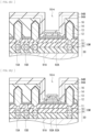
- FIG. 1 schematically illustrates an example of a cross-sectional configuration of a light-emitting device (a light-emitting device 1) according to a first embodiment of the present disclosure.
- FIG. 2 schematically illustrates an example of a planar configuration of the light-emitting device 1 illustrated in FIG. 1, and FIG. 1 illustrates a cross-section corresponding to a line I-I' illustrated in FIG. 2 .
- the light-emitting device 1 is suitably applicable as a display pixel of a display apparatus (e.g., an image display apparatus 100, see FIG. 5 ) called a so-called LED display.
- the light-emitting device 1 of the present embodiment has, for example, a configuration in which multiple nano-column type light-emitting elements (columnar structures 12) are provided on an insulating layer 11, and in which a partition wall 17 having an inclined surface of less than 90° relative to a surface of the insulating layer 11 is provided between adjacent columnar structures.
- the light-emitting device 1 includes a light-emitting section 10 including the multiple columnar structures 12, a wavelength conversion section 20 provided on a side of a light output surface 10S1 of the light-emitting section 10, and a drive substrate 30 provided on a side of a wiring layer 10E of the light-emitting section 10.
- a light-emitting section 10 including the multiple columnar structures 12, a wavelength conversion section 20 provided on a side of a light output surface 10S1 of the light-emitting section 10, and a drive substrate 30 provided on a side of a wiring layer 10E of the light-emitting section 10.
- the light-emitting section 10 includes the insulating layer 11 having a first surface 11S1 and a second surface 11S2 opposed to each other, the multiple columnar structures 12 arranged in matrix, for example, a p-electrode 13 and a passivation film 14 covering a side surface and a top surface of each of the multiple columnar structures 12, and an n-electrode 15A penetrating the insulating layer 11 from a side of the second surface 11S2 to be in contact with the columnar structure 12, an insulating film 16 embedding the multiple columnar structures 12, and the partition wall 17 provided between adjacent columnar structures 12.
- FIG. 3 schematically illustrates an example of a cross-sectional configuration of the columnar structure 12.
- the columnar structure 12 is, for example, a nano-column type light-emitting diode (LED), and includes, for example, an n-type crystalline structure 12A, an active layer 12B, and a p-type semiconductor layer 12C.
- LED nano-column type light-emitting diode
- the n-type crystalline structure 12A is provided on a buffer layer 42 stacked on a growth substrate 41, inside an opening 11H provided in a mask layer 11A, and is formed by, for example, an n-type GaN-based semiconductor material (see, e.g., FIG. 4B ), although detailed description is given later.
- the n-type crystalline structure 12A is erected in a perpendicular direction (Z-axis direction) on the buffer layer 42 in a substantially hexagonal column shape, for example, as illustrated in FIGs. 1 and 2 , and has a shape in which an area of the side surface thereof is larger than an area of the top surface thereof.
- This n-type crystalline structure 12A corresponds to a specific example of a "columnar crystalline structure" of the present disclosure.
- the active layer 12B is provided, for example, along the side surface and the top surface of the n-type crystalline structure 12A.
- the active layer 12B has, for example, a multiquantum well structure in which InGaN and GaN are alternately stacked, and has a light-emitting region in the layer.
- the active layer 12B emits light in a blue band having an emission wavelength of 430 nm or more and 500 nm or less.
- This active layer 12B corresponds to a specific example of an "active layer" of the present disclosure.
- the p-type semiconductor layer 12C is provided along a side surface and a top surface of the active layer 12B.
- the p-type semiconductor layer 12C is formed by, for example, a p-type GaN-based semiconductor material.
- This p-type semiconductor layer 12C corresponds to a specific example of a "semiconductor layer" of the present disclosure.
- the p-electrode 13 covers a periphery of the p-type semiconductor layer 12C, and is provided as a common layer for the multiple columnar structures 12.
- the p-electrode 13 is formed by, for example, a transparent electrode material such as ITO (Indiun Tin Oxide), IZO, SnO, or TiO.
- the passivation film 14 is provided to protect the surface of the columnar structure 12, and covers a side surface and a top surface the p-electrode 13, for example; in addition, the passivation film 14 is provided as a common layer for the multiple columnar structures 12.
- the passivation film 14 is formed by, for example, SiO, SiN, or the like.
- the n-electrodes 15A are provided independently of each other in the respective multiple columnar structures 12, and each penetrate the insulating layer 11 from the side of the second surface 11S2 of the insulating layer 11 to be in contact with the n-type crystalline structure 12A as described above.
- a p-electrode pad 15B penetrating the insulating layer 11 to be electrically coupled to the p-electrode 13 and a pad electrode 15C to be electrically coupled to the partition wall 17 are further provided, for example, between adjacent columnar structures 12 in the same layer as the n-electrode 15A on the side of the second surface 11S2 of the insulating layer 11.
- the n-electrode 15A, the p-electrode pad 15B, and the pad electrode 15C are each formed using a transparent electrode material such as ITO or IZO, for example.
- the n-electrode 15A, the p-electrode pad 15B, and the pad electrode 15C can be formed using a metal material such as palladium (Pd), titanium (Ti), aluminum (Al), platinum (Pt), silver (Ag), nickel (Ni), or gold (Au), for example.
- the insulating film 16 embeds the multiple columnar structures 12, and forms the planar light output surface 10S1 of the light-emitting section 10.
- the insulating film 16 is formed by, for example, SiO, SiN, or the like.
- the partition wall 17 is provided to suppress occurrence of color mixture due to optical leakage to between adjacent RGB sub-pixels when applying the light-emitting device 1 to a display pixel 123 of the image display apparatus 100 described later.
- the partition wall 17 is provided in a grid pattern to partition the multiple columnar structures 12 arranged in matrix.
- the partition wall 17 has an inclined surface of less than 90° relative to the first surface 11 S1 of the insulating layer 11, for example, in a cross-sectional view. That is, the partition wall 17 has a forward tapered shape in a cross-sectional view.
- This partition wall 17 corresponds to a specific example of a "light-blocking member" of the present disclosure.
- the partition wall 17 includes, for example, a light-blocking film 17A and an insulating film 17B covering a side surface and a top surface of the light-blocking film 17A. It is preferable for the light-blocking film 17A to have a light-blocking property and to be formed using a material further having light reflectivity. Examples of such a material include Al, Ag, and rhodium (Rh).
- the insulating film 17B is provided to reduce galvanic corrosion between the p-electrode 13 including, for example, ITO and the light-blocking film 17A including, for example, Al, and is formed by, for example, silicon oxide (SiO), silicon nitride (SiN), or the like.
- the partition wall 17 having a forward tapered shape and further forming the light-blocking film 17A using a material having the light-blocking property and the light reflectivity, light emitted from the side surface of the columnar structure 12 is reflected by the inclined surface of the partition wall 17 to the light output surface 10S1. This improves light extraction efficiency.
- the partition wall 17 penetrates the insulating layer 11, and the bottom of the light-blocking film 17A is exposed to the side of the second surface 11S2 of the insulating layer 11.
- the light-blocking film 17A is electrically coupled to, for example, the pad electrode 15C described later, and is coupled to, for example, GND. This suppresses abnormal electric discharge in the light-blocking film 17A.
- the light-emitting section 10 further includes a wiring layer 10W on the side of the second surface 11S2 of the insulating layer 11.
- the wiring layer 10W forms a bonded surface 10S2 with the drive substrate 30.
- the wiring layer 10W includes, in an insulating layer 18, multiple contact electrodes 19 to be each electrically coupled to the n-electrode 15A, the p-electrode pad 15B, and the pad electrode 15C.
- the multiple contact electrodes 19 are each configured by, for example, a copper (Cu) pad, and exposed to the bonded surface 10S2. These multiple contact electrodes 19 correspond to a specific example of "first contact electrodes" of the present disclosure.
- the wavelength conversion section 20 includes color conversion layers 21 (a red color conversion layer 21R, a green color conversion layer 21G, and a blue color conversion layer 21B) disposed above the multiple columnar structures 12, an insulating film 22 and a separation part 23 disposed between the color conversion layers 21R, 21G, and 21B, an insulating film 24 covering side surfaces of the insulating film 22 and the separation part 23, and a protective layer 25.
- color conversion layers 21 a red color conversion layer 21R, a green color conversion layer 21G, and a blue color conversion layer 21B
- the color conversion layers 21 are each provided to convert light emitted from the multiple columnar structures 12 into a desired wavelength (e.g., red (R)/green (G)/blue (B)) for emission.
- the red color conversion layer 21R, the green color conversion layer 21G, and the blue color conversion layer 21B can be formed to include and using quantum dots corresponding to the respective colors.
- the quantum dots can be selected from InP, GaInP, InAsP, CdSe, CdZnSe, CdTeSe, CdTe, or the like, for example.
- the quantum dots can be selected from InP, GaInP, ZnSeTe, ZnTe, CdSe, CdZnSe, CdS CdSeS, or the like, for example.
- the quantum dots can be selected from ZnSe, ZnTe, ZnSeTe, CdSe, CdZnSe, CdS, CdZnS, CdSeS, and the like. It is to be noted that, in a case where blue light is emitted from the columnar structure 12 as described above, the blue color conversion layer 21B may be formed by a resin layer having light transmissivity.
- the separation part 23 is provided to suppress occurrence of color mixture due to optical leakage to between adjacent RGB sub-pixels when applying the light-emitting device 1 to the display pixel 123 of the image display apparatus 100.
- the separation part 23 includes, for example, a silicon (Si) substrate 23A and a light-blocking film (unillustrated) having a light-blocking property and light reflectivity, for example, which are described later.
- the insulating films 22 and 24 are each formed by, for example, SiO, SiN, or the like.
- the protective layer 25 is provided to protect a surface of the light-emitting device 1, and is formed by, for example, SiO, SiN, or the like.
- the drive substrate 30 includes a semiconductor substrate 31 and a wiring layer 30W to be in contact with the bonded surface 10S2 of the light-emitting section 10.
- the wiring layer 30W for example, multiple wiring lines 33 and multiple contact electrodes 34 are stacked in order inside an insulating layer 32 from a side of the semiconductor substrate 31.
- the multiple contact electrodes 34 are each configured by, for example, a copper (Cu) pad, and exposed to a surface of the insulating layer 32.
- Cu copper
- the light-emitting device 1 can be produced, for example, as follows.
- FIGs. 4A to 4N illustrate a method of manufacturing the light-emitting device 1 in the order of steps.
- the buffer layer 42 is formed on the growth substrate 41, and then, for example, a chemical vapor deposition method (CVD method) is used to form the mask layer 11A having the opening 11H at a predetermined position, for example, on the buffer layer 42.
- CVD method chemical vapor deposition method
- the n-type crystalline structure 12A, the active layer 12B, and the p-type semiconductor layer 12C are sequentially grown on the buffer layer 42 exposed inside the opening 11H by means of epitaxial growth to form the columnar structure 12.
- an atomic layer deposition method ALD method
- ALD method atomic layer deposition method
- a CVD method is used to form the insulating film 16 including, for example, SiO on the passivation film 14 to embed the columnar structure 12, and then, for example, a CMP (Chemical Mechanical Polishing) method is used to planarize a surface of the insulating film 16.
- CMP Chemical Mechanical Polishing
- an Si substrate 23A is attached onto the insulating film 16 with the insulating film 22 interposed therebetween, and then inversion is performed.
- the growth substrate 41 and the buffer layer 42 are removed as illustrated in FIG. 4F , and then an opening 17H penetrating the mask layer 11A, the p-electrode 13, the passivation film 14, and the insulating film 16 is formed, between adjacent columnar structures 12, from a side of the mask layer 11A as illustrated in FIG. 4F .
- an ALD method is used to form the insulating film 17B including, for example, SiO on the mask layer 11A, the n-type crystalline structure 12A of the columnar structure 12, and a side surface and a bottom surface of the opening 17H.
- the light-blocking film 17A including, for example, Al is formed to fill the opening 17H, and then, for example, etch-back is used to remove the light-blocking film 17A formed outside the opening 17H.
- an insulating film including, for example, SiO is further formed on the light-blocking film 17A and the insulating film 17B, and then, as illustrated in FIG. 4H , for example, photolithography and etching are used to form openings 15H1 and 15H2 exposing the n-type crystalline structure 12A of the columnar structure 12 and the light-blocking film 17A, respectively.
- photolithography and etching are used to form an opening 15H3 exposing the p-electrode 13.
- a sputtering method is used to form a metal film including, for example, Ti inside the openings 15H1, 15H2, and 15H3, and then patterning is performed by photolithography and etching to form the n-electrode 15A, the p-electrode pad 15B, and the pad electrode 15C, respectively.
- a CVD method is used to form the insulating layer 18 including, for example, SiO to cover the insulating layer 11, the n-electrode 15A, the p-electrode pad 15B, and the pad electrode 15C.
- a method similar to that described above is used to form the contact electrode 19 to be electrically coupled to each of the n-electrode 15A, the p-electrode pad 15B, and the pad electrode 15C, and a surface thereof is planarized to form the bonded surface 10S2.
- the contact electrode 19 exposed to the bonded surface 10S2 and the contact electrode 34 exposed to a surface of the wiring layer 30W of the drive substrate 30 prepared separately are attached together by Cu-Cu bonding, for example.
- the Si substrate 23A is worked to form an opening 23H above each of the columnar structures 12. Then, for example, formation of an oxide film such as SiO and etch-back as well as formation of a light-blocking film and etch-back allow for formation of the separation part 23 above the partition wall 17, for example.
- the insulating film 24 including, for example, SiO is formed, which is continuous on the side surface and a top surface of the separation parts 23 and between the separation parts 23.
- corresponding color conversion layers 21 red color conversion layer 21R, green color conversion layer 21G, and blue color conversion layer 21B
- the protective layer 25 is formed.
- FIG. 5 is a perspective view of an example of an outline configuration of a display apparatus (image display apparatus 100) of the present disclosure.
- the image display apparatus 100 is called a so-called LED display, and uses the light-emitting device 1 of the present embodiment as a display pixel.
- the image display apparatus 100 includes a display panel 110 and a control circuit 140 that drives the display panel 110.
- the display panel 110 includes a mounting substrate 120 and a counter substrate 130 which are overlapped each other.
- the counter substrate 130 has a surface serving as a picture display surface, and has a display region 100A at a middle portion thereof as well as a frame region 100B being a non-display region around the display region 100A.
- FIG. 6 illustrates an example of a wiring layout of a region, corresponding to the display region 100A, of a surface of the mounting substrate 120 on a side of the counter substrate 130.
- multiple data wiring lines 121 are formed to extend in a predetermined direction, and are arranged in parallel at a predetermined pitch.
- multiple scan wiring lines 122 are further formed to extend in a direction intersecting (e.g., orthogonal to) the data wiring lines 121, and are arranged in parallel at a predetermined pitch.
- the data wiring line 121 and the scan wiring line 122 each include, for example, an electrically-conductive material such as Cu (copper).
- the scan wiring lines 122 are formed on, for example, an uppermost layer, and is formed on, for example, an insulating layer (unillustrated) formed on a surface of a base material.
- a base material of the mounting substrate 120 includes, for example, a silicon substrate, a resin substrate, or the like, and that the insulating layer on the base material includes, for example, silicon nitride (SiN), silicon oxide (SiO), aluminum oxide (AlO), or a resin material.
- the data wiring lines 121 are formed inside a layer different from the uppermost layer including the scan wiring lines 122 (e.g., a layer under the uppermost layer), and is formed, for example, inside the insulating layer on the base material.
- a periphery of an intersecting portion of the data wiring line 121 and the scan wiring line 122 corresponds to the display pixel 123, and multiple display pixels 123 are arranged in a matrix shape within the display region 100A.
- Each of the display pixels 123 is mounted with the light-emitting device 1 including light-emitting sections corresponding to R, G, and B, for example.
- FIG. 6 exemplifies a case where three light-emitting sections R, G, and B constitute one display pixel 123 to enable the light-emitting section R, the light-emitting section G, and the light-emitting section B to output red light, green light, and blue light, respectively.
- the light-emitting device 1 is provided with, for example, a pair of terminal electrodes disposed for each of the light-emitting sections R, G, and B, or provided with terminal electrodes one of which is shared by the light-emitting sections R, G, and B and another of which is disposed for each of the light-emitting sections R, G, and B.
- the one of the terminal electrodes is electrically coupled to the data wiring line 121
- the other of the terminal electrodes is electrically coupled to the scan wiring line 122.
- the one of the terminal electrodes is electrically coupled to a pad electrode 121B at the tip of a branch 121A provided in the data wiring line 121.
- the other of the terminal electrodes is electrically coupled to a pad electrode 122B at the tip of a branch 122A provided in the scan wiring line 122.
- Each of the pad electrodes 121B and 122B is formed, for example, in the uppermost layer, and is provided, for example, at a location where each light-emitting device 1 is mounted, as illustrated in FIG. 6 .
- the pad electrodes 121B and 122B each include, for example, an electrically-conductive material such as Au (gold).
- the mounting substrate 120 is further provided with, for example, multiple support columns (unillustrated) to regulate an interval between the mounting substrate 120 and the counter substrate 130.
- the support column may be provided within a region facing the display region 100A, or may be provided within a region facing the frame region 100B.
- the counter substrate 130 includes, for example, a glass substrate, a resin substrate, or the like.
- a surface of the counter substrate 130 on a side of the light-emitting device 1 may be planar, but is preferably a rough surface.
- the rough surface may be provided across the entire region facing the display region 100A, or may be provided only in a region facing the display pixel 123.
- the rough surface has fine unevenness on which light beams emitted from the light-emitting sections R, G, and B are incident on the rough surface.
- the unevenness of the rough surface can be prepared by, for example, sandblasting, dry etching, or the like.
- the control circuit 140 drives each display pixel 123 (each light-emitting device 1) on the basis of a picture signal.
- the control circuit 140 is configured by, for example, a data driver that drives the data wiring lines 121 coupled to the display pixel 123 and a scan driver that drives the scan wiring lines 122 coupled to the display pixel 123.
- the control circuit 140 may be provided separately from the display panel 110 and coupled to the mounting substrate 120 via a wiring line, or may be mounted on the mounting substrate 120.
- the partition wall 17 having an inclined surface of less than 90° relative to the first surface 11S1 of the insulating layer 11 is provided between adjacent columnar structures 12. This suppresses optical leakage to adjacent RGB sub-pixels when using the light-emitting device 1 in the display pixel 123 of the image display apparatus 100, for example.
- the light-emitting device 1 of the present embodiment it is possible, in the light-emitting device 1 of the present embodiment, to suppress occurrence of color mixture. Thus, it is possible to improve display quality of the image display apparatus 100 including the light-emitting device 1.
- the light-blocking film 17A constituting the partition wall 17 is formed using a material having light reflectivity in addition to a light-blocking property. This allows light emitted from the side surface of the columnar structure 12 to be reflected by the inclined surface of the partition wall 17 to the light output surface 10S1. Thus, it is possible to improve light extraction efficiency.
- the multiple columnar structures 12 are formed, and then formation is performed from the side of the surface (second surface 11S2 of insulating layer 11) on a side opposite to the light output surface 10S1, thus making it possible to easily form the partition wall 17 having a forward tapered shape in which the inclined surface has an angle of less than 90° as described above.
- fine working is possible as compared with a case where the formation is performed prior to the multiple columnar structures 12.
- the pad electrode 15C is coupled to the light-blocking film 17A constituting the partition wall 17 to apply a fixed potential, thus suppressing abnormal electric discharge due to a floating state.
- the pad electrode 15C is coupled to the light-blocking film 17A constituting the partition wall 17 to apply a fixed potential, thus suppressing abnormal electric discharge due to a floating state.
- the p-electrode 13 is used as a common electrode for the multiple columnar structures 12, and the p-electrode pad 15B to be electrically coupled to the p-electrode 13 is further provided on the side of the second surface 11S2 of the insulating layer 11 immediately below the partition wall 17, thus making it possible to achieve a narrower pitch. This makes it possible to achieve higher definition in the image display apparatus 100 including the same.
- FIG. 7 schematically illustrates an example of a cross-sectional configuration of a light-emitting device (a light-emitting device 1A) according to Modification Example 1 of the present disclosure.
- the light-emitting device 1A of the present modification example differs from the foregoing first embodiment in that a light-blocking film 57A of a partition wall 57 and a separation part 63 are each formed using, for example, a resin material such as a black resist.
- the foregoing first embodiment has given the example in which the partition wall 17 is configured by the light-blocking film 17A having a light-blocking property and light reflectivity and the insulating film 17B provided therearound and the example in which the separation part 23 is configured by the Si substrate and the light-blocking film having a light-blocking property and light reflectivity.
- this is not limitative.
- the pad electrode 15C for applying a fixed potential to the partition wall 17 formed in the foregoing first embodiment and the contact electrode 19 to be electrically coupled thereto can be omitted.
- the separation part 23 need not have both the light-blocking property and the light-reflectivity.
- the light-blocking film constituting the separation part 23 may be omitted, for example, in the foregoing first embodiment.
- the separation part 23 may be configured by a worked Si substrate and an insulating film including, for example, SiO or the like, or may be configured only by a worked Si substrate.
- FIGs. 8A and 8B each schematically illustrate another example of the planar configuration of the light-emitting device 1 of the foregoing first embodiment.
- the foregoing first embodiment has given the example in which the partition wall 17 is provided, for example, in a grid pattern between adjacent columnar structures 12; however, this is not limitative.
- the partition wall 17 may be formed to surround each of the multiple columnar structures 12 in a circular shape in a plan view.
- each of the multiple columnar structures 12 may be formed in a polygonal shape in a plan view.
- the insulating film 16 covering the side surface of the columnar structure 12 may be omitted so as to form the columnar structure 12 to allow the side surface of the columnar structure 12 and the partition wall 17 to be in contact with each other.
- FIG. 9 schematically illustrates an example of a cross-sectional configuration of a light-emitting device 1B according to Modification Example 3 of the present disclosure.
- the foregoing first embodiment has given the example of using the nano-column type light-emitting element (columnar structure 12).
- the present technology is applicable also to a planar type light-emitting element as illustrated in FIG. 9 , and is able to achieve effects similar to those of the foregoing first embodiment.
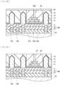
- FIG. 10 schematically illustrates an example of a cross-sectional configuration of a light-emitting device (a light-emitting device 2) according to a second embodiment of the present disclosure.
- the light-emitting device 2 is suitably applicable as a display pixel of a display apparatus (e.g., image display apparatus 100) called a so-called LED display.
- the light-emitting device 2 of the present embodiment differs from the foregoing first embodiment in that, for example, a partition wall 77 is formed from the side of the light output surface 10S1.
- the light-emitting device 2 can be manufactured, for example, as follows.
- FIGs. 11A to 11C illustrate a method of manufacturing the light-emitting device 2 in the order of steps.
- a chemical vapor deposition method (CVD method) is used to form, for example, a mask layer 82 having an opening at a predetermined position, on the insulating film 16.
- CVD method chemical vapor deposition method
- DET Double Exposure Technology
- a CVD method is used to form, for example, Al as a film to fill the opening 77H1, and then, for example, etch-back is used to remove the Al film formed outside the opening 77H1 and the mask layer 82, thus forming the partition wall 77 including Al.
- the wavelength conversion section 20 is formed on the light output surface 10S1.
- the partition wall 77 having a forward tapered shape in which the inclined surface has an angle of less than 90° can also be formed from the side of the light output surface 10S1.
- the partition wall 77 is formed after formation of the multiple columnar structures 12, thus enabling fine working, as compared with the case where the formation is performed prior to the multiple columnar structures 12.
- FIG. 12 schematically illustrates an example of a cross-sectional configuration of a light-emitting device (a light-emitting device 2A) according to Modification Example 4 of the present disclosure.
- the light-emitting device 2A of the present modification example differs from the foregoing second embodiment in that a printing technique is used to form the partition wall 77 from the side of the light output surface 10S1.
- the light-emitting device 2A can be produced, for example, as follows.
- FIGs. 13A to 13F illustrate a method of manufacturing the light-emitting device 2 in the order of steps.
- the columnar structure 12 is formed, and the drive substrate 30 is attached thereto with the wiring layer 10W interposed therebetween. Thereafter, inversion is performed, and a support substrate (unillustrated) attached onto the insulating film 16 is removed. Subsequently, as illustrated in FIG. 13A , for example, a lithography technique is used to form, for example, a mask layer 83 having an opening at a predetermined position on the insulating film 16. Thereafter, for example, dry etching is used to form an opening 77H2 penetrating the insulating film 16.
- the mask layer 83 is removed by, for example, wet etching.
- a lithography technique is used to form a mask layer 84 on a side surface of the opening 77H2, and the opening 77H2 is allowed to have a forward tapered shape.
- printing is used to form a light-blocking film 77A including, for example, Al inside the opening 77H2. This allows for formation of the light-blocking film 77A having a forward tapered shape inside the opening 77H2.
- FIG. 13D for example, wet etching is used to remove the mask layer 84 formed inside the opening 77H.
- a CVD method is used to form an insulating film 77B including, for example, SiO in the opening 77H2
- a CMP method is used to planarize a surface of the insulating film 77B.
- the wavelength conversion section 20 is formed on the light output surface 10S1.
- the partition wall 77 having a forward tapered shape in which the inclined surface has an angle of less than 90° can also be formed using a printing technique.
- FIG. 14 schematically illustrates an example of a cross-sectional configuration of a light-emitting device (a light-emitting device 2B) according to a Modification Example 5 of the present disclosure.
- the light-emitting device 2B of the present modification example differs from the foregoing second embodiment in that a partition wall 97 to be provided between adjacent columnar structures 12 is formed using multiple wiring lines formed in a peripheral region 10Y around a light-emitting region 10X provided with the multiple columnar structures 12.
- the peripheral region 10Y is provided with, for example, a wiring layer 90W in which multiple wiring lines 91, 92, and 93 are stacked and formed, and the multiple wiring lines 91, 92, and 93 constitute, for example, a logic circuit, or the like.
- the light-emitting device 2B can be produced, for example, as follows.
- FIGs. 15A to 15N illustrate a method of manufacturing the light-emitting device 2 in the order of steps.
- a lithography technique is used to form, for example, a mask layer 85 having an opening 85H at a predetermined position on the insulating film 16.
- dry etching is used to form an opening 16H penetrating the insulating film 16.
- the mask layer 85 is removed, and then, as illustrated in FIG. 15C , for example, a sputtering method is used to form an electrically-conductive film 91X including, for example, Al, which is continuous on the insulating film 16 and on a side surface and a bottom surface of the opening 16H.
- a lithography technique is used to form a mask layer 86 inside the opening 16H, and then wet etching is performed. This allows for formation of a light-blocking film 91A having an inclined surface on a side surface thereof, which is the first layer of the partition wall 97, inside the opening 16H.
- a CVD method is used to form an insulating film 94A on the insulating film 16 and on the side surface and the bottom surface of the opening 16H.
- a lithography technique is used to form, on the insulating film 94A, a mask layer 87 having an opening at a predetermined position inside the opening 16H.
- dry etching is used to form an opening 94H penetrating to the light-blocking film 91A.
- the mask layer 87 is removed, and then, as illustrated in FIG. 15G , an electrically-conductive film 92X including, for example, Al is formed to fill the opening 94H.
- a lithography technique is used to form a mask layer 88 inside the opening 16H, and then wet etching is performed. This allows for formation of a light-blocking film 92A having an inclined surface on a side surface thereof, which is the second layer of the partition wall 97, inside the opening 16H.
- a CVD method is used to form an insulating film 94B on the insulating film 94A.
- a similar method is used to form a light-blocking film 93A which is the third layer of the partition wall 97, inside the opening 16H.
- a CVD method is used to form an insulating film 94 to fill the opening 16H.
- a CMP method is used to remove the insulating film 94 provided on the insulating film 16.
- a mask layer 89 having an opening at a predetermined position is formed, and then, for example, dry etching is used to form the opening 94H penetrating the insulating film 94 to the light-blocking film 93A.
- the light-emitting device 2B illustrated in FIG. 14 is completed.
- the partition wall 97 provided between adjacent columnar structures 12 may be formed using the multiple wiring lines 91, 92, and 93 formed in the peripheral region 10Y and constituting a logic circuit, for example.
- a multilayer wiring layer e.g., wiring lines 91, 92, and 93
- FIG. 16 is a perspective view of another configuration example (an image display apparatus 200) of the display apparatus using the light-emitting device (e.g., light-emitting device 1) of the present disclosure.
- the image display apparatus 200 is called a so-called tiling display in which an LED is used as a light source, and the light-emitting device 1 of the present embodiment is used as a display pixel.
- the image display apparatus 200 includes a display panel 210 and a control circuit 240 that drives the display panel 210.
- the display panel 210 includes a mounting substrate 220 and a counter substrate 230 which are overlapped each other.
- the counter substrate 230 has a surface serving as a picture display surface, and has a display region at a middle portion thereof as well as a frame region being a non-display region around the display region (none of which is illustrated).
- the counter substrate 230 is disposed at a position facing the mounting substrate 220 with a predetermined gap interposed therebetween. It is to be noted that the counter substrate 230 may be in contact with a top surface of the mounting substrate 220.
- FIG. 17 schematically illustrates an example of a configuration of the mounting substrate 220.
- the mounting substrate 220 is configured by multiple unit substrates 250 laid in a tile shape. It is to be noted that FIG. 17 illustrates the example in which the mounting substrate 220 is configured by nine unit substrates 250; however, the number of the unit substrates 250 may be ten or more, or may be eight or less.
- FIG. 18 illustrates an example of a configuration of the unit substrate 250.
- the unit substrate 250 includes, for example, the light-emitting devices 1 including multiple light-emitting sections (e.g., light-emitting sections A1, A2, A3, A4, A5, and A6) laid in a tile shape, and a support substrate 260 that supports the respective light-emitting devices 1.
- Each of the unit substrates 250 further includes a control substrate (unillustrated).
- the support substrate 260 is configured by, for example, a metal frame (metal plate), a wiring substrate, or the like. In a case where the support substrate 260 is configured by a wiring substrate, it may also be possible for the support substrate 260 to serve as a control substrate. At this time, at least one of the support substrate 260 or the control substrate is electrically coupled to each of the light-emitting devices 1.
- the foregoing embodiments and the like have given the examples in which the light-emitting device 1 or the like is applied to the image display apparatus 100, 200, or the like; however, the light-emitting device 1 or the like of the present disclosure can also be used as an illumination apparatus.
- the present technology may also have the following configurations. According to the present technology of the following configurations, there is provided, between multiple columnar structures erected on a first surface of an insulating layer having the first surface and a second surface opposed to each other, a light-blocking member having an inclined surface of less than 90° relative to the first surface. This makes it possible to reduce optical leakage to adjacent columnar structures. Thus, it is possible to suppress occurrence of color mixture.
Landscapes
- Physics & Mathematics (AREA)
- General Physics & Mathematics (AREA)
- Engineering & Computer Science (AREA)
- Theoretical Computer Science (AREA)
- Electroluminescent Light Sources (AREA)
- Devices For Indicating Variable Information By Combining Individual Elements (AREA)
- Led Device Packages (AREA)
- Led Devices (AREA)
Abstract
Description
- The present disclosure relates to, for example, a light-emitting device including multiple light-emitting sections and a display apparatus including the light-emitting device.
- For example,
PTL 1 discloses a light-emitting device in which an optical confinement factor is increased by providing a light propagation layer and providing thereabove and therebelow low-refractive-index parts each having a refractive index lower than that of the light propagation layer, between multiple columnar parts in which a first semiconductor layer, an active layer, and a second semiconductor layer are stacked in this order. - PTL 1:
Japanese Unexamined Patent Application Publication No. 2019-054127 - Incidentally, a light-emitting device including multiple light-emitting sections each including a light-emitting diode (LED) is required to suppress color mixture between adjacent light-emitting sections.
- It is desirable to provide a light-emitting device that makes it possible to suppress occurrence of color mixture and a display apparatus including the light-emitting device.
- A light-emitting device of an embodiment of the present disclosure includes: an insulating layer having a first surface and a second surface that are opposed to each other; multiple columnar structures each including a columnar crystalline structure of a first electrically-conductive type erected in a direction perpendicular to the first surface of the insulating layer, and an active layer and a semiconductor layer of a second electrically-conductive type that are stacked in this order on a side surface and a top surface of the columnar crystalline structure; and a light-blocking member provided between the multiple columnar structures and having an inclined surface of less than 90° relative to the first surface.
- A display apparatus of an embodiment of the present disclosure includes the light-emitting device of the embodiment as one or multiple light-emitting devices.
- In the light-emitting device of an embodiment of the present disclosure and the display apparatus of an embodiment of the present disclosure, the light-blocking member having an inclined surface of less than 90° relative to the first surface is provided between the multiple columnar structures erected on the first surface of the insulating layer having the first surface and the second surface opposed to each other. This allows for suppression of optical leakage to adjacent columnar structures.
-
- [
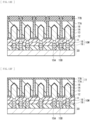
FIG. 1] FIG. 1 is a schematic cross-sectional view of an example of a configuration of a light-emitting device according to a first embodiment of the present disclosure. - [
FIG. 2] FIG. 2 is a schematic view of an example of a planar configuration of the light-emitting device illustrated inFIG. 1 . - [
FIG. 3] FIG. 3 is a schematic cross-sectional view of an example of a configuration of a columnar structure illustrated inFIG. 1 . - [
FIG. 4A] FIG. 4A is an explanatory schematic cross-sectional view of an example of a step of manufacturing the light-emitting device illustrated inFIG. 1 . - [
FIG. 4B] FIG. 4B is a schematic cross-sectional view of a step subsequent toFIG. 4A . - [
FIG. 4C] FIG. 4C is a schematic cross-sectional view of a step subsequent toFIG. 4B . - [
FIG. 4D] FIG. 4D is a schematic cross-sectional view of a step subsequent toFIG. 4C . - [
FIG. 4E] FIG. 4E is a schematic cross-sectional view of a step subsequent toFIG. 4D . - [
FIG.4F] FIG. 4F is a schematic cross-sectional view of a step subsequent toFIG. 4E . - [
FIG. 4G] FIG. 4G is a schematic cross-sectional view of a step subsequent toFIG. 4F . - [
FIG. 4H] FIG. 4H is a schematic cross-sectional view of a step subsequent toFIG. 4G . - [
FIG. 4I] FIG. 4I is a schematic cross-sectional view of a step subsequent toFIG. 4H . - [
FIG.4J] FIG. 4J is a schematic cross-sectional view of a step subsequent toFIG. 4I . - [
FIG. 4K] FIG. 4K is a schematic cross-sectional view of a step subsequent toFIG. 4J . - [
FIG.4L] FIG. 4L is a schematic cross-sectional view of a step subsequent toFIG. 4K . - [
FIG. 4M] FIG. 4M is a schematic cross-sectional view of a step subsequent toFIG. 4L . - [
FIG.4N] FIG. 4N is a schematic cross-sectional view of a step subsequent toFIG. 4M . - [
FIG. 5] FIG. 5 is a perspective view of an example of a configuration of a display apparatus including the light-emitting device of the present disclosure. - [
FIG. 6] FIG. 6 is a schematic view of an example of a wiring layout of the image display apparatus illustrated inFIG. 5 . - [
FIG. 7] FIG. 7 is a schematic cross-sectional view of an example of a configuration of a light-emitting device according to Modification Example 1 of the present disclosure. - [
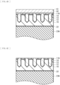
FIG. 8A] FIG. 8A is a schematic view of an example of a planar configuration of a configuration of a light-emitting device according to Modification Example 2 of the present disclosure. - [
FIG. 8B] FIG. 8B is a schematic view of another example of the planar configuration of the configuration of the light-emitting device according to Modification Example 2 of the present disclosure. - [
FIG. 9] FIG. 9 is a schematic cross-sectional view of an example of a configuration of a light-emitting device according to Modification Example 3 of the present disclosure. - [
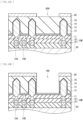
FIG. 10] FIG. 10 is a schematic cross-sectional view of an example of a configuration of a light-emitting device according to a second embodiment of the present disclosure. - [
FIG. 11A] FIG. 11A is an explanatory schematic cross-sectional view of an example of a step of manufacturing the light-emitting device illustrated inFIG. 10 . - [
FIG. 11B] FIG. 11B is a schematic cross-sectional view of a step subsequent toFIG. 11A . - [
FIG. 11C] FIG. 11C is a schematic cross-sectional view of a step subsequent toFIG. 11B . - [
FIG. 12] FIG. 12 is a schematic cross-sectional view of an example of a configuration of a light-emitting device according to Modification Example 4 of the present disclosure. - [
FIG. 13A] FIG. 13A is an explanatory schematic cross-sectional view of an example of a step of manufacturing the light-emitting device illustrated inFIG. 12 . - [
FIG. 13B] FIG. 13B is a schematic cross-sectional view of a step subsequent toFIG. 13A . - [
FIG. 13C] FIG. 13C is a schematic cross-sectional view of a step subsequent toFIG. 13B . - [
FIG. 13D] FIG. 13D is a schematic cross-sectional view of a step subsequent toFIG. 13C . - [
FIG. 13E] FIG. 13E is a schematic cross-sectional view of a step subsequent toFIG. 13D . - [
FIG. 13F] FIG. 13F is a schematic cross-sectional view of a step subsequent toFIG. 13E . - [
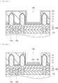
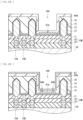
FIG. 14] FIG. 14 is a schematic cross-sectional view of an example of a configuration of a light-emitting device according to Modification Example 5 of the present disclosure. - [
FIG. 15A] FIG. 15A is an explanatory schematic cross-sectional view of an example of a step of manufacturing the light-emitting device illustrated inFIG. 14 . - [
FIG. 15B] FIG. 15B is a schematic cross-sectional view of a step subsequent toFIG. 15A . - [
FIG. 15C] FIG. 15C is a schematic cross-sectional view of a step subsequent toFIG. 15B . - [
FIG. 15D] FIG. 15D is a schematic cross-sectional view of a step subsequent toFIG. 15C . - [
FIG. 15E] FIG. 15E is a schematic cross-sectional view of a step subsequent toFIG. 15D . - [
FIG. 15F] FIG. 15F is a schematic cross-sectional view of a step subsequent toFIG. 15E . - [
FIG. 15G] FIG. 15G is a schematic cross-sectional view of a step subsequent toFIG. 15F . - [
FIG. 15H] FIG. 15H is a schematic cross-sectional view of a step subsequent toFIG. 15G . - [
FIG. 15I] FIG. 15I is a schematic cross-sectional view of a step subsequent toFIG. 15H . - [
FIG. 15J] FIG. 15J is a schematic cross-sectional view of a step subsequent toFIG. 15I . - [
FIG. 15K] FIG. 15K is a schematic cross-sectional view of a step subsequent toFIG. 15J . - [
FIG. 15L] FIG. 15L is a schematic cross-sectional view of a step subsequent toFIG. 15K . - [
FIG. 15M] FIG. 15M is a schematic cross-sectional view of a step subsequent toFIG. 15L . - [
FIG. 15N] FIG. 15N is a schematic cross-sectional view of a step subsequent toFIG. 15M . - [
FIG. 16] FIG. 16 is a perspective view of another example of the configuration of the display apparatus including the light-emitting device of the present disclosure. - [
FIG. 17] FIG. 17 is a perspective view of a configuration of a mounting substrate illustrated inFIG. 16 . - [
FIG. 18] FIG. 18 is a perspective view of a configuration of a unit substrate illustrated inFIG. 17 . - In the following, description is given in detail of embodiments of the present disclosure with reference to the drawings. The following description is merely a specific example of the present disclosure, and the present disclosure should not be limited to the following aspects. Moreover, the present disclosure is not limited to arrangements, dimensions, dimensional ratios, and the like of each component illustrated in the drawings. It is to be noted that the description is given in the following order.
- 1. First Embodiment (An example of a light-emitting device provided with a partition wall having an inclined surface of less than 90° between adjacent light-emitting elements)
- 1-1. Configuring of Light-Emitting Device
- 1-2. Method of Manufacturing Light-Emitting Device
- 1-3. Configuration of Display Apparatus
- 1-4. Workings and Effects
- 2. Modification Example 1 (An example of formation of a partition wall using a black resist)
- 3. Modification Example 2 (An example of using a planar type LED)
- 4. Modification Example 3 (Another example of a planar shape of a partition wall)
- 5. Second Embodiment (Another example of a light-emitting device provided with a partition wall having an inclined surface of less than 90° between adjacent light-emitting elements)
- 6. Modification Example 4 (Another example of a manufacturing method)
- 7. Modification Example 5 (An example of formation of a partition wall using logic wiring lines)
- 8. Modification Example 6 (Another example of display apparatus)
-
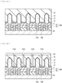
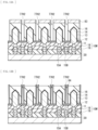
FIG. 1 schematically illustrates an example of a cross-sectional configuration of a light-emitting device (a light-emitting device 1) according to a first embodiment of the present disclosure.FIG. 2 schematically illustrates an example of a planar configuration of the light-emittingdevice 1 illustrated inFIG. 1, and FIG. 1 illustrates a cross-section corresponding to a line I-I' illustrated inFIG. 2 . The light-emittingdevice 1 is suitably applicable as a display pixel of a display apparatus (e.g., animage display apparatus 100, seeFIG. 5 ) called a so-called LED display. The light-emittingdevice 1 of the present embodiment has, for example, a configuration in which multiple nano-column type light-emitting elements (columnar structures 12) are provided on an insulatinglayer 11, and in which apartition wall 17 having an inclined surface of less than 90° relative to a surface of the insulatinglayer 11 is provided between adjacent columnar structures. - As described above, the light-emitting
device 1 includes a light-emittingsection 10 including the multiplecolumnar structures 12, awavelength conversion section 20 provided on a side of a light output surface 10S1 of the light-emittingsection 10, and adrive substrate 30 provided on a side of a wiring layer 10E of the light-emittingsection 10. Hereinafter, description is given in detail of the light-emittingsection 10, thewavelength conversion section 20, and thedrive substrate 30. - The light-emitting
section 10 includes the insulatinglayer 11 having a first surface 11S1 and a second surface 11S2 opposed to each other, the multiplecolumnar structures 12 arranged in matrix, for example, a p-electrode 13 and apassivation film 14 covering a side surface and a top surface of each of the multiplecolumnar structures 12, and an n-electrode 15A penetrating the insulatinglayer 11 from a side of the second surface 11S2 to be in contact with thecolumnar structure 12, an insulatingfilm 16 embedding the multiplecolumnar structures 12, and thepartition wall 17 provided between adjacentcolumnar structures 12. -
FIG. 3 schematically illustrates an example of a cross-sectional configuration of thecolumnar structure 12. Thecolumnar structure 12 is, for example, a nano-column type light-emitting diode (LED), and includes, for example, an n-type crystalline structure 12A, anactive layer 12B, and a p-type semiconductor layer 12C. - The n-
type crystalline structure 12A is provided on abuffer layer 42 stacked on agrowth substrate 41, inside anopening 11H provided in amask layer 11A, and is formed by, for example, an n-type GaN-based semiconductor material (see, e.g.,FIG. 4B ), although detailed description is given later. The n-type crystalline structure 12A is erected in a perpendicular direction (Z-axis direction) on thebuffer layer 42 in a substantially hexagonal column shape, for example, as illustrated inFIGs. 1 and2 , and has a shape in which an area of the side surface thereof is larger than an area of the top surface thereof. This n-type crystalline structure 12A corresponds to a specific example of a "columnar crystalline structure" of the present disclosure. - The
active layer 12B is provided, for example, along the side surface and the top surface of the n-type crystalline structure 12A. Theactive layer 12B has, for example, a multiquantum well structure in which InGaN and GaN are alternately stacked, and has a light-emitting region in the layer. For example, theactive layer 12B emits light in a blue band having an emission wavelength of 430 nm or more and 500 nm or less. Thisactive layer 12B corresponds to a specific example of an "active layer" of the present disclosure. - The p-
type semiconductor layer 12C is provided along a side surface and a top surface of theactive layer 12B. The p-type semiconductor layer 12C is formed by, for example, a p-type GaN-based semiconductor material. This p-type semiconductor layer 12C corresponds to a specific example of a "semiconductor layer" of the present disclosure. - The p-
electrode 13 covers a periphery of the p-type semiconductor layer 12C, and is provided as a common layer for the multiplecolumnar structures 12. The p-electrode 13 is formed by, for example, a transparent electrode material such as ITO (Indiun Tin Oxide), IZO, SnO, or TiO. - The
passivation film 14 is provided to protect the surface of thecolumnar structure 12, and covers a side surface and a top surface the p-electrode 13, for example; in addition, thepassivation film 14 is provided as a common layer for the multiplecolumnar structures 12. Thepassivation film 14 is formed by, for example, SiO, SiN, or the like. - The n-
electrodes 15A are provided independently of each other in the respective multiplecolumnar structures 12, and each penetrate the insulatinglayer 11 from the side of the second surface 11S2 of the insulatinglayer 11 to be in contact with the n-type crystalline structure 12A as described above. In addition, a p-electrode pad 15B penetrating the insulatinglayer 11 to be electrically coupled to the p-electrode 13 and apad electrode 15C to be electrically coupled to thepartition wall 17 are further provided, for example, between adjacentcolumnar structures 12 in the same layer as the n-electrode 15A on the side of the second surface 11S2 of the insulatinglayer 11. The n-electrode 15A, the p-electrode pad 15B, and thepad electrode 15C are each formed using a transparent electrode material such as ITO or IZO, for example. In addition thereto, the n-electrode 15A, the p-electrode pad 15B, and thepad electrode 15C can be formed using a metal material such as palladium (Pd), titanium (Ti), aluminum (Al), platinum (Pt), silver (Ag), nickel (Ni), or gold (Au), for example. - The insulating
film 16 embeds the multiplecolumnar structures 12, and forms the planar light output surface 10S1 of the light-emittingsection 10. The insulatingfilm 16 is formed by, for example, SiO, SiN, or the like. - The
partition wall 17 is provided to suppress occurrence of color mixture due to optical leakage to between adjacent RGB sub-pixels when applying the light-emittingdevice 1 to adisplay pixel 123 of theimage display apparatus 100 described later. For example, as illustrated inFIG. 2 , thepartition wall 17 is provided in a grid pattern to partition the multiplecolumnar structures 12 arranged in matrix. In the present embodiment, thepartition wall 17 has an inclined surface of less than 90° relative to thefirst surface 11 S1 of the insulatinglayer 11, for example, in a cross-sectional view. That is, thepartition wall 17 has a forward tapered shape in a cross-sectional view. Thispartition wall 17 corresponds to a specific example of a "light-blocking member" of the present disclosure. - The
partition wall 17 includes, for example, a light-blockingfilm 17A and an insulatingfilm 17B covering a side surface and a top surface of the light-blockingfilm 17A. It is preferable for the light-blockingfilm 17A to have a light-blocking property and to be formed using a material further having light reflectivity. Examples of such a material include Al, Ag, and rhodium (Rh). The insulatingfilm 17B is provided to reduce galvanic corrosion between the p-electrode 13 including, for example, ITO and the light-blockingfilm 17A including, for example, Al, and is formed by, for example, silicon oxide (SiO), silicon nitride (SiN), or the like. As described, by forming thepartition wall 17 having a forward tapered shape and further forming the light-blockingfilm 17A using a material having the light-blocking property and the light reflectivity, light emitted from the side surface of thecolumnar structure 12 is reflected by the inclined surface of thepartition wall 17 to the light output surface 10S1. This improves light extraction efficiency. - In the present embodiment, the
partition wall 17 penetrates the insulatinglayer 11, and the bottom of the light-blockingfilm 17A is exposed to the side of the second surface 11S2 of the insulatinglayer 11. The light-blockingfilm 17A is electrically coupled to, for example, thepad electrode 15C described later, and is coupled to, for example, GND. This suppresses abnormal electric discharge in the light-blockingfilm 17A. - The light-emitting
section 10 further includes awiring layer 10W on the side of the second surface 11S2 of the insulatinglayer 11. Thewiring layer 10W forms a bonded surface 10S2 with thedrive substrate 30. Thewiring layer 10W includes, in an insulatinglayer 18,multiple contact electrodes 19 to be each electrically coupled to the n-electrode 15A, the p-electrode pad 15B, and thepad electrode 15C. Themultiple contact electrodes 19 are each configured by, for example, a copper (Cu) pad, and exposed to the bonded surface 10S2. Thesemultiple contact electrodes 19 correspond to a specific example of "first contact electrodes" of the present disclosure. - The
wavelength conversion section 20 includes color conversion layers 21 (a redcolor conversion layer 21R, a greencolor conversion layer 21G, and a bluecolor conversion layer 21B) disposed above the multiplecolumnar structures 12, an insulatingfilm 22 and aseparation part 23 disposed between the color conversion layers 21R, 21G, and 21B, an insulatingfilm 24 covering side surfaces of the insulatingfilm 22 and theseparation part 23, and aprotective layer 25. - The color conversion layers 21 (red
color conversion layer 21R, greencolor conversion layer 21G, and bluecolor conversion layer 21B) are each provided to convert light emitted from the multiplecolumnar structures 12 into a desired wavelength (e.g., red (R)/green (G)/blue (B)) for emission. The redcolor conversion layer 21R, the greencolor conversion layer 21G, and the bluecolor conversion layer 21B can be formed to include and using quantum dots corresponding to the respective colors. Specifically, in a case where red light is obtained, the quantum dots can be selected from InP, GaInP, InAsP, CdSe, CdZnSe, CdTeSe, CdTe, or the like, for example. In a case where green light is obtained, the quantum dots can be selected from InP, GaInP, ZnSeTe, ZnTe, CdSe, CdZnSe, CdS CdSeS, or the like, for example. In a case where blue light is obtained, the quantum dots can be selected from ZnSe, ZnTe, ZnSeTe, CdSe, CdZnSe, CdS, CdZnS, CdSeS, and the like. It is to be noted that, in a case where blue light is emitted from thecolumnar structure 12 as described above, the bluecolor conversion layer 21B may be formed by a resin layer having light transmissivity. - Similarly to the
partition wall 17 described above, theseparation part 23 is provided to suppress occurrence of color mixture due to optical leakage to between adjacent RGB sub-pixels when applying the light-emittingdevice 1 to thedisplay pixel 123 of theimage display apparatus 100. Theseparation part 23 includes, for example, a silicon (Si)substrate 23A and a light-blocking film (unillustrated) having a light-blocking property and light reflectivity, for example, which are described later. - The insulating
films protective layer 25 is provided to protect a surface of the light-emittingdevice 1, and is formed by, for example, SiO, SiN, or the like. - The
drive substrate 30 includes asemiconductor substrate 31 and awiring layer 30W to be in contact with the bonded surface 10S2 of the light-emittingsection 10. In thewiring layer 30W, for example,multiple wiring lines 33 andmultiple contact electrodes 34 are stacked in order inside an insulatinglayer 32 from a side of thesemiconductor substrate 31. Similarly to themultiple contact electrodes 19 described above, themultiple contact electrodes 34 are each configured by, for example, a copper (Cu) pad, and exposed to a surface of the insulatinglayer 32. Thesemultiple contact electrodes 34 correspond to a specific example of "second contact electrodes" of the present disclosure. - The light-emitting
device 1 can be produced, for example, as follows.FIGs. 4A to 4N illustrate a method of manufacturing the light-emittingdevice 1 in the order of steps. - First, as illustrated in
FIG. 4A , thebuffer layer 42 is formed on thegrowth substrate 41, and then, for example, a chemical vapor deposition method (CVD method) is used to form themask layer 11A having theopening 11H at a predetermined position, for example, on thebuffer layer 42. - Subsequently, as illustrated in
FIG. 4B , the n-type crystalline structure 12A, theactive layer 12B, and the p-type semiconductor layer 12C are sequentially grown on thebuffer layer 42 exposed inside theopening 11H by means of epitaxial growth to form thecolumnar structure 12. Next, as illustrated inFIG. 4C , for example, an atomic layer deposition method (ALD method) is used to form, as a film, the p-electrode 13 which is continuous on the top surface and the side surface of thecolumnar structure 12 and on themask layer 11A, and then thepassivation film 14 is formed on the p-electrode 13. Further, as illustrated inFIG. 4C , for example, a CVD method is used to form the insulatingfilm 16 including, for example, SiO on thepassivation film 14 to embed thecolumnar structure 12, and then, for example, a CMP (Chemical Mechanical Polishing) method is used to planarize a surface of the insulatingfilm 16. - Subsequently, as illustrated in
FIG. 4D , anSi substrate 23A is attached onto the insulatingfilm 16 with the insulatingfilm 22 interposed therebetween, and then inversion is performed. Next, as illustrated inFIG. 4E , thegrowth substrate 41 and thebuffer layer 42 are removed as illustrated inFIG. 4F , and then anopening 17H penetrating themask layer 11A, the p-electrode 13, thepassivation film 14, and the insulatingfilm 16 is formed, between adjacentcolumnar structures 12, from a side of themask layer 11A as illustrated inFIG. 4F . - Subsequently, as illustrated in
FIG. 4G , for example, an ALD method is used to form the insulatingfilm 17B including, for example, SiO on themask layer 11A, the n-type crystalline structure 12A of thecolumnar structure 12, and a side surface and a bottom surface of theopening 17H. Next, similarly, the light-blockingfilm 17A including, for example, Al is formed to fill theopening 17H, and then, for example, etch-back is used to remove the light-blockingfilm 17A formed outside theopening 17H. - Subsequently, an insulating film including, for example, SiO is further formed on the light-blocking
film 17A and the insulatingfilm 17B, and then, as illustrated inFIG. 4H , for example, photolithography and etching are used to form openings 15H1 and 15H2 exposing the n-type crystalline structure 12A of thecolumnar structure 12 and the light-blockingfilm 17A, respectively. Next, as illustrated inFIG. 4I , for example, photolithography and etching are used to form an opening 15H3 exposing the p-electrode 13. - Subsequently, as illustrated in a cross-sectional view (A) and a plan view (B) of
FIG. 4J , for example, a sputtering method is used to form a metal film including, for example, Ti inside the openings 15H1, 15H2, and 15H3, and then patterning is performed by photolithography and etching to form the n-electrode 15A, the p-electrode pad 15B, and thepad electrode 15C, respectively. - Next, as illustrated in a cross-sectional view (A) and a plan view (B) of
FIG. 4K , for example, a CVD method is used to form the insulatinglayer 18 including, for example, SiO to cover the insulatinglayer 11, the n-electrode 15A, the p-electrode pad 15B, and thepad electrode 15C. Thereafter, a method similar to that described above is used to form thecontact electrode 19 to be electrically coupled to each of the n-electrode 15A, the p-electrode pad 15B, and thepad electrode 15C, and a surface thereof is planarized to form the bonded surface 10S2. - Subsequently, as illustrated in
FIG. 4L , thecontact electrode 19 exposed to the bonded surface 10S2 and thecontact electrode 34 exposed to a surface of thewiring layer 30W of thedrive substrate 30 prepared separately are attached together by Cu-Cu bonding, for example. - Next, as illustrated in
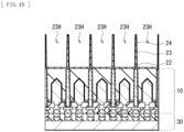
FIG. 4M , theSi substrate 23A is worked to form anopening 23H above each of thecolumnar structures 12. Then, for example, formation of an oxide film such as SiO and etch-back as well as formation of a light-blocking film and etch-back allow for formation of theseparation part 23 above thepartition wall 17, for example. Subsequently, as illustrated inFIG. 4N , the insulatingfilm 24 including, for example, SiO is formed, which is continuous on the side surface and a top surface of theseparation parts 23 and between theseparation parts 23. Thereafter, corresponding color conversion layers 21 (redcolor conversion layer 21R, greencolor conversion layer 21G, and bluecolor conversion layer 21B) are formed inside theopening 23H, and then theprotective layer 25 is formed. Through the above-described steps, the light-emittingdevice 1 illustrated inFIG. 1 is completed. -
FIG. 5 is a perspective view of an example of an outline configuration of a display apparatus (image display apparatus 100) of the present disclosure. Theimage display apparatus 100 is called a so-called LED display, and uses the light-emittingdevice 1 of the present embodiment as a display pixel. As illustrated inFIG. 5 , for example, theimage display apparatus 100 includes adisplay panel 110 and acontrol circuit 140 that drives thedisplay panel 110. - The
display panel 110 includes a mountingsubstrate 120 and acounter substrate 130 which are overlapped each other. Thecounter substrate 130 has a surface serving as a picture display surface, and has adisplay region 100A at a middle portion thereof as well as aframe region 100B being a non-display region around thedisplay region 100A. -
FIG. 6 illustrates an example of a wiring layout of a region, corresponding to thedisplay region 100A, of a surface of the mountingsubstrate 120 on a side of thecounter substrate 130. In the region, corresponding to thedisplay region 100A, of the surface of the mountingsubstrate 120, for example, as illustrated inFIG. 6 , multipledata wiring lines 121 are formed to extend in a predetermined direction, and are arranged in parallel at a predetermined pitch. In the region, corresponding to thedisplay region 100A, of the surface of the mountingsubstrate 120, for example, multiplescan wiring lines 122 are further formed to extend in a direction intersecting (e.g., orthogonal to) thedata wiring lines 121, and are arranged in parallel at a predetermined pitch. Thedata wiring line 121 and thescan wiring line 122 each include, for example, an electrically-conductive material such as Cu (copper). - The
scan wiring lines 122 are formed on, for example, an uppermost layer, and is formed on, for example, an insulating layer (unillustrated) formed on a surface of a base material. It is to be noted that a base material of the mountingsubstrate 120 includes, for example, a silicon substrate, a resin substrate, or the like, and that the insulating layer on the base material includes, for example, silicon nitride (SiN), silicon oxide (SiO), aluminum oxide (AlO), or a resin material. Meanwhile, thedata wiring lines 121 are formed inside a layer different from the uppermost layer including the scan wiring lines 122 (e.g., a layer under the uppermost layer), and is formed, for example, inside the insulating layer on the base material. - A periphery of an intersecting portion of the
data wiring line 121 and thescan wiring line 122 corresponds to thedisplay pixel 123, andmultiple display pixels 123 are arranged in a matrix shape within thedisplay region 100A. Each of thedisplay pixels 123 is mounted with the light-emittingdevice 1 including light-emitting sections corresponding to R, G, and B, for example. It is to be noted thatFIG. 6 exemplifies a case where three light-emitting sections R, G, and B constitute onedisplay pixel 123 to enable the light-emitting section R, the light-emitting section G, and the light-emitting section B to output red light, green light, and blue light, respectively. - The light-emitting
device 1 is provided with, for example, a pair of terminal electrodes disposed for each of the light-emitting sections R, G, and B, or provided with terminal electrodes one of which is shared by the light-emitting sections R, G, and B and another of which is disposed for each of the light-emitting sections R, G, and B. In addition, the one of the terminal electrodes is electrically coupled to thedata wiring line 121, and the other of the terminal electrodes is electrically coupled to thescan wiring line 122. For example, the one of the terminal electrodes is electrically coupled to apad electrode 121B at the tip of abranch 121A provided in thedata wiring line 121. Further, for example, the other of the terminal electrodes is electrically coupled to apad electrode 122B at the tip of abranch 122A provided in thescan wiring line 122. - Each of the
pad electrodes device 1 is mounted, as illustrated inFIG. 6 . Here, thepad electrodes - The mounting
substrate 120 is further provided with, for example, multiple support columns (unillustrated) to regulate an interval between the mountingsubstrate 120 and thecounter substrate 130. The support column may be provided within a region facing thedisplay region 100A, or may be provided within a region facing theframe region 100B. - The
counter substrate 130 includes, for example, a glass substrate, a resin substrate, or the like. A surface of thecounter substrate 130 on a side of the light-emittingdevice 1 may be planar, but is preferably a rough surface. The rough surface may be provided across the entire region facing thedisplay region 100A, or may be provided only in a region facing thedisplay pixel 123. The rough surface has fine unevenness on which light beams emitted from the light-emitting sections R, G, and B are incident on the rough surface. The unevenness of the rough surface can be prepared by, for example, sandblasting, dry etching, or the like. - The
control circuit 140 drives each display pixel 123 (each light-emitting device 1) on the basis of a picture signal. Thecontrol circuit 140 is configured by, for example, a data driver that drives thedata wiring lines 121 coupled to thedisplay pixel 123 and a scan driver that drives thescan wiring lines 122 coupled to thedisplay pixel 123. For example, as illustrated inFIG. 5 , thecontrol circuit 140 may be provided separately from thedisplay panel 110 and coupled to the mountingsubstrate 120 via a wiring line, or may be mounted on the mountingsubstrate 120. - In the present embodiment, for example, the
partition wall 17 having an inclined surface of less than 90° relative to the first surface 11S1 of the insulatinglayer 11 is provided between adjacentcolumnar structures 12. This suppresses optical leakage to adjacent RGB sub-pixels when using the light-emittingdevice 1 in thedisplay pixel 123 of theimage display apparatus 100, for example. - As described above, it is possible, in the light-emitting
device 1 of the present embodiment, to suppress occurrence of color mixture. Thus, it is possible to improve display quality of theimage display apparatus 100 including the light-emittingdevice 1. - In addition, in the present embodiment, the light-blocking
film 17A constituting thepartition wall 17 is formed using a material having light reflectivity in addition to a light-blocking property. This allows light emitted from the side surface of thecolumnar structure 12 to be reflected by the inclined surface of thepartition wall 17 to the light output surface 10S1. Thus, it is possible to improve light extraction efficiency. - Further, in the present embodiment, the multiple
columnar structures 12 are formed, and then formation is performed from the side of the surface (second surface 11S2 of insulating layer 11) on a side opposite to the light output surface 10S1, thus making it possible to easily form thepartition wall 17 having a forward tapered shape in which the inclined surface has an angle of less than 90° as described above. In addition, for example, fine working is possible as compared with a case where the formation is performed prior to the multiplecolumnar structures 12. - Furthermore, in the present embodiment, the
pad electrode 15C is coupled to the light-blockingfilm 17A constituting thepartition wall 17 to apply a fixed potential, thus suppressing abnormal electric discharge due to a floating state. Thus, it is possible to improve reliability of theimage display apparatus 100 including the same. - In addition, in the present embodiment, the p-
electrode 13 is used as a common electrode for the multiplecolumnar structures 12, and the p-electrode pad 15B to be electrically coupled to the p-electrode 13 is further provided on the side of the second surface 11S2 of the insulatinglayer 11 immediately below thepartition wall 17, thus making it possible to achieve a narrower pitch. This makes it possible to achieve higher definition in theimage display apparatus 100 including the same. - Next, description is given of a second embodiment of the present disclosure and modification examples (Modification Example 1 to 6). Hereinafter, components similar to those of the foregoing first embodiment are denoted by the same reference numerals, and descriptions thereof are omitted as appropriate.
-
FIG. 7 schematically illustrates an example of a cross-sectional configuration of a light-emitting device (a light-emittingdevice 1A) according to Modification Example 1 of the present disclosure. The light-emittingdevice 1A of the present modification example differs from the foregoing first embodiment in that a light-blockingfilm 57A of apartition wall 57 and aseparation part 63 are each formed using, for example, a resin material such as a black resist. - As described above, the foregoing first embodiment has given the example in which the
partition wall 17 is configured by the light-blockingfilm 17A having a light-blocking property and light reflectivity and the insulatingfilm 17B provided therearound and the example in which theseparation part 23 is configured by the Si substrate and the light-blocking film having a light-blocking property and light reflectivity. However, this is not limitative. - It is to be noted that, in a case where a black resist is used to form the
partition wall 57 as in the present modification example, thepad electrode 15C for applying a fixed potential to thepartition wall 17 formed in the foregoing first embodiment and thecontact electrode 19 to be electrically coupled thereto can be omitted. - In addition, the
separation part 23 need not have both the light-blocking property and the light-reflectivity. For example, the light-blocking film constituting theseparation part 23 may be omitted, for example, in the foregoing first embodiment. In that case, theseparation part 23 may be configured by a worked Si substrate and an insulating film including, for example, SiO or the like, or may be configured only by a worked Si substrate. -
FIGs. 8A and8B each schematically illustrate another example of the planar configuration of the light-emittingdevice 1 of the foregoing first embodiment. The foregoing first embodiment has given the example in which thepartition wall 17 is provided, for example, in a grid pattern between adjacentcolumnar structures 12; however, this is not limitative. - For example, as illustrated in
FIG. 8A , thepartition wall 17 may be formed to surround each of the multiplecolumnar structures 12 in a circular shape in a plan view. Alternatively, for example, as illustrated inFIG. 8B , each of the multiplecolumnar structures 12 may be formed in a polygonal shape in a plan view. It is to be noted that, as illustrated inFIG. 8B , in a case of adopting a hexagonal shape similarly to the planar shape of thecolumnar structure 12, the insulatingfilm 16 covering the side surface of thecolumnar structure 12 may be omitted so as to form thecolumnar structure 12 to allow the side surface of thecolumnar structure 12 and thepartition wall 17 to be in contact with each other. -
FIG. 9 schematically illustrates an example of a cross-sectional configuration of a light-emittingdevice 1B according to Modification Example 3 of the present disclosure. The foregoing first embodiment has given the example of using the nano-column type light-emitting element (columnar structure 12). However, the present technology is applicable also to a planar type light-emitting element as illustrated inFIG. 9 , and is able to achieve effects similar to those of the foregoing first embodiment. -
FIG. 10 schematically illustrates an example of a cross-sectional configuration of a light-emitting device (a light-emitting device 2) according to a second embodiment of the present disclosure. Similarly to the foregoing first embodiment, the light-emittingdevice 2 is suitably applicable as a display pixel of a display apparatus (e.g., image display apparatus 100) called a so-called LED display. The light-emittingdevice 2 of the present embodiment differs from the foregoing first embodiment in that, for example, apartition wall 77 is formed from the side of the light output surface 10S1. - The light-emitting
device 2 can be manufactured, for example, as follows.FIGs. 11A to 11C illustrate a method of manufacturing the light-emittingdevice 2 in the order of steps. - First, a method similar to that of the foregoing first embodiment is used to form the
columnar structure 12 and attach thedrive substrate 30 thereto with thewiring layer 10W interposed therebetween. Thereafter, as illustrated inFIG. 11A , inversion is performed, and a support substrate (unillustrated) attached onto the insulatingfilm 16 is removed. - Subsequently, as illustrated in
FIG. 11B , for example, a chemical vapor deposition method (CVD method) is used to form, for example, amask layer 82 having an opening at a predetermined position, on the insulatingfilm 16. Thereafter, for example, DET (Double Exposure Technology) is used to penetrate the insulatingfilm 16 and to form an opening 77H1 having a forward tapered shape. Next, as illustrated inFIG. 11C , for example, a CVD method is used to form, for example, Al as a film to fill the opening 77H1, and then, for example, etch-back is used to remove the Al film formed outside the opening 77H1 and themask layer 82, thus forming thepartition wall 77 including Al. Thereafter, thewavelength conversion section 20 is formed on the light output surface 10S1. Through the above-described steps, the light-emittingdevice 2 illustrated inFIG. 10 is completed. - As described above, the
partition wall 77 having a forward tapered shape in which the inclined surface has an angle of less than 90° can also be formed from the side of the light output surface 10S1. In addition, similarly to the foregoing first embodiment, thepartition wall 77 is formed after formation of the multiplecolumnar structures 12, thus enabling fine working, as compared with the case where the formation is performed prior to the multiplecolumnar structures 12. -
FIG. 12 schematically illustrates an example of a cross-sectional configuration of a light-emitting device (a light-emittingdevice 2A) according to Modification Example 4 of the present disclosure. The light-emittingdevice 2A of the present modification example differs from the foregoing second embodiment in that a printing technique is used to form thepartition wall 77 from the side of the light output surface 10S1. - The light-emitting
device 2A can be produced, for example, as follows.FIGs. 13A to 13F illustrate a method of manufacturing the light-emittingdevice 2 in the order of steps. - First, similarly to the foregoing second embodiment, the
columnar structure 12 is formed, and thedrive substrate 30 is attached thereto with thewiring layer 10W interposed therebetween. Thereafter, inversion is performed, and a support substrate (unillustrated) attached onto the insulatingfilm 16 is removed. Subsequently, as illustrated inFIG. 13A , for example, a lithography technique is used to form, for example, amask layer 83 having an opening at a predetermined position on the insulatingfilm 16. Thereafter, for example, dry etching is used to form an opening 77H2 penetrating the insulatingfilm 16. - Next, the
mask layer 83 is removed by, for example, wet etching. Thereafter, as illustrated inFIG. 13B , for example, a lithography technique is used to form amask layer 84 on a side surface of the opening 77H2, and the opening 77H2 is allowed to have a forward tapered shape. Subsequently, as illustrated inFIG. 13C , for example, printing is used to form a light-blockingfilm 77A including, for example, Al inside the opening 77H2. This allows for formation of the light-blockingfilm 77A having a forward tapered shape inside the opening 77H2. - Next, as illustrated in
FIG. 13D , for example, wet etching is used to remove themask layer 84 formed inside the opening 77H. Subsequently, as illustrated inFIG. 13E , for example, a CVD method is used to form an insulatingfilm 77B including, for example, SiO in the opening 77H2, and then, as illustrated inFIG. 13F , for example, a CMP method is used to planarize a surface of the insulatingfilm 77B. Thereafter, thewavelength conversion section 20 is formed on the light output surface 10S1. Through the above-described steps, the light-emittingdevice 2A illustrated inFIG. 12 is completed. - In this manner, the
partition wall 77 having a forward tapered shape in which the inclined surface has an angle of less than 90° can also be formed using a printing technique. -
FIG. 14 schematically illustrates an example of a cross-sectional configuration of a light-emitting device (a light-emittingdevice 2B) according to a Modification Example 5 of the present disclosure. The light-emittingdevice 2B of the present modification example differs from the foregoing second embodiment in that apartition wall 97 to be provided between adjacentcolumnar structures 12 is formed using multiple wiring lines formed in aperipheral region 10Y around a light-emittingregion 10X provided with the multiplecolumnar structures 12. - The
peripheral region 10Y is provided with, for example, awiring layer 90W in whichmultiple wiring lines multiple wiring lines - The light-emitting
device 2B can be produced, for example, as follows.FIGs. 15A to 15N illustrate a method of manufacturing the light-emittingdevice 2 in the order of steps. - First, as illustrated in
FIG. 15A , similarly to the foregoing Modification Example 4, for example, a lithography technique is used to form, for example, amask layer 85 having anopening 85H at a predetermined position on the insulatingfilm 16. Subsequently, as illustrated inFIG. 15B , dry etching is used to form anopening 16H penetrating the insulatingfilm 16. - Next, the
mask layer 85 is removed, and then, as illustrated inFIG. 15C , for example, a sputtering method is used to form an electrically-conductive film 91X including, for example, Al, which is continuous on the insulatingfilm 16 and on a side surface and a bottom surface of theopening 16H. Subsequently, as illustrated inFIG. 15D , for example, a lithography technique is used to form amask layer 86 inside theopening 16H, and then wet etching is performed. This allows for formation of a light-blockingfilm 91A having an inclined surface on a side surface thereof, which is the first layer of thepartition wall 97, inside theopening 16H. - Next, as illustrated in
FIG. 15E , for example, a CVD method is used to form an insulatingfilm 94A on the insulatingfilm 16 and on the side surface and the bottom surface of theopening 16H. Subsequently, as illustrated inFIG. 15F , for example, a lithography technique is used to form, on the insulatingfilm 94A, amask layer 87 having an opening at a predetermined position inside theopening 16H. Thereafter, dry etching is used to form anopening 94H penetrating to the light-blockingfilm 91A. Next, themask layer 87 is removed, and then, as illustrated inFIG. 15G , an electrically-conductive film 92X including, for example, Al is formed to fill theopening 94H. - Subsequently, as illustrated in
FIG. 15H , for example, a lithography technique is used to form amask layer 88 inside theopening 16H, and then wet etching is performed. This allows for formation of a light-blockingfilm 92A having an inclined surface on a side surface thereof, which is the second layer of thepartition wall 97, inside theopening 16H. Next, as illustrated inFIG. 15I , for example, a CVD method is used to form an insulatingfilm 94B on the insulatingfilm 94A. Subsequently, as illustrated inFIG. 15J , a similar method is used to form a light-blockingfilm 93A which is the third layer of thepartition wall 97, inside theopening 16H. - Next, as illustrated in
FIG. 15K , for example, a CVD method is used to form an insulatingfilm 94 to fill theopening 16H. Subsequently, as illustrated inFIG. 15L , for example, a CMP method is used to remove the insulatingfilm 94 provided on the insulatingfilm 16. Next, as illustrated inFIG. 15M , amask layer 89 having an opening at a predetermined position is formed, and then, for example, dry etching is used to form theopening 94H penetrating the insulatingfilm 94 to the light-blockingfilm 93A. - Subsequently, for example, wet etching is used to remove the
mask layer 89, and then, as illustrated inFIG. 15N , for example, a sputtering method and etch-back are used to form a metal film including, for example, Al, inside theopening 94H. This allows for formation of thepartition wall 97. Thereafter, thewavelength conversion section 20 is formed on the light output surface 10S1. Through the above-described steps, the light-emittingdevice 2B illustrated inFIG. 14 is completed. - As described above, the
partition wall 97 provided between adjacentcolumnar structures 12 may be formed using themultiple wiring lines peripheral region 10Y and constituting a logic circuit, for example. By forming thepartition wall 97 using a multilayer wiring layer (e.g.,wiring lines peripheral region 10Y, it is possible to form thepartition wall 97 simultaneously in a formation step of the logic circuit. Thus, it is possible to reduce manufacturing steps as compared with the case of separately forming (e.g., the partition wall 77) as in the foregoing second embodiment, etc. -
FIG. 16 is a perspective view of another configuration example (an image display apparatus 200) of the display apparatus using the light-emitting device (e.g., light-emitting device 1) of the present disclosure. Theimage display apparatus 200 is called a so-called tiling display in which an LED is used as a light source, and the light-emittingdevice 1 of the present embodiment is used as a display pixel. For example, as illustrated inFIG. 16 , theimage display apparatus 200 includes adisplay panel 210 and acontrol circuit 240 that drives thedisplay panel 210. - The
display panel 210 includes a mountingsubstrate 220 and acounter substrate 230 which are overlapped each other. Thecounter substrate 230 has a surface serving as a picture display surface, and has a display region at a middle portion thereof as well as a frame region being a non-display region around the display region (none of which is illustrated). For example, thecounter substrate 230 is disposed at a position facing the mountingsubstrate 220 with a predetermined gap interposed therebetween. It is to be noted that thecounter substrate 230 may be in contact with a top surface of the mountingsubstrate 220. -
FIG. 17 schematically illustrates an example of a configuration of the mountingsubstrate 220. For example, as illustrated inFIG. 17 , the mountingsubstrate 220 is configured bymultiple unit substrates 250 laid in a tile shape. It is to be noted thatFIG. 17 illustrates the example in which the mountingsubstrate 220 is configured by nineunit substrates 250; however, the number of theunit substrates 250 may be ten or more, or may be eight or less. -
FIG. 18 illustrates an example of a configuration of theunit substrate 250. Theunit substrate 250 includes, for example, the light-emittingdevices 1 including multiple light-emitting sections (e.g., light-emitting sections A1, A2, A3, A4, A5, and A6) laid in a tile shape, and asupport substrate 260 that supports the respective light-emittingdevices 1. Each of theunit substrates 250 further includes a control substrate (unillustrated). Thesupport substrate 260 is configured by, for example, a metal frame (metal plate), a wiring substrate, or the like. In a case where thesupport substrate 260 is configured by a wiring substrate, it may also be possible for thesupport substrate 260 to serve as a control substrate. At this time, at least one of thesupport substrate 260 or the control substrate is electrically coupled to each of the light-emittingdevices 1. - Description has been given hereinabove of the present disclosure referring to the first and second embodiments and Modification Example 1 to 6; however, the present disclosure is not limited to the foregoing embodiments, and may be modified in a wide variety of ways. For example, the components, the arrangement, the number, and the like of the light-emitting element (columnar structure 12) exemplified in the foregoing embodiments, and the like are merely exemplary. All of the components need not be included, and other components may further be included.
- In addition, the foregoing embodiments and the like have given the examples in which the light-emitting
device 1 or the like is applied to theimage display apparatus device 1 or the like of the present disclosure can also be used as an illumination apparatus. - It is to be noted that the effects described herein are merely exemplary and are not limited thereto, and may further include other effects.
- The present technology may also have the following configurations. According to the present technology of the following configurations, there is provided, between multiple columnar structures erected on a first surface of an insulating layer having the first surface and a second surface opposed to each other, a light-blocking member having an inclined surface of less than 90° relative to the first surface. This makes it possible to reduce optical leakage to adjacent columnar structures. Thus, it is possible to suppress occurrence of color mixture.
- (1) A light-emitting device including:
- an insulating layer having a first surface and a second surface that are opposed to each other;
- multiple columnar structures each including a columnar crystalline structure of a first electrically-conductive type erected in a direction perpendicular to the first surface of the insulating layer, and an active layer and a semiconductor layer of a second electrically-conductive type that are stacked in this order on a side surface and a top surface of the columnar crystalline structure; and
- a light-blocking member provided between the multiple columnar structures and having an inclined surface of less than 90° relative to the first surface.
- (2) The light-emitting device according to (1), in which the light-blocking member has light reflectivity.
- (3) The light-emitting device according to (1) or (2), in which the light-blocking member has a forward tapered shape.
- (4) The light-emitting device according to any one of (1) to (3), in which the light-blocking member includes multiple wiring layers.
- (5) The light-emitting device according to any one of (1) to (4), further including:
- a first electrode to be in contact with the columnar crystalline structure of each of the multiple columnar structures from the second surface of the insulating layer; and
- a second electrode that continuously covers a side surface and a top surface of the semiconductor layer of each of the multiple columnar structures on a side of the first surface of the insulating layer.
- (6) The light-emitting device according to (5), further including a drive substrate provided on a side of the second surface of the insulating layer and being electrically coupled to the columnar structures and the semiconductor layer via the first electrode and the second electrode.
- (7) The light-emitting device according to (6), in which the light-blocking member penetrates the second electrode and the insulating layer.
- (8) The light-emitting device according to any one of (1) to (7), in which the light-blocking member includes an electrically-conductive material.
- (9) The light-emitting device according to any one of (6) to (8), further including a wiring layer including multiple first contact electrodes each exposed to a surface facing the drive substrate on the side of the second surface of the insulating layer, in which
the first electrode, the second electrode, and the light-blocking member are electrically coupled to each of the multiple first contact electrodes. - (10) The light-emitting device according to (9), in which
- the drive substrate further includes multiple second contact electrodes each exposed to a surface facing the insulating layer, and
- the insulating layer and the drive substrate are bonded to each other via the first contact electrodes and the second contact electrodes.
- (11) The light-emitting device according to any one of (1) to (10), in which
- the multiple columnar structures are provided in matrix on the first surface of the insulating layer, and
- the light-blocking member is provided in a grid pattern on the first surface of the insulating layer.
- (12) The light-emitting device according to any one of (1) to (11), further including an insulating film provided on the first surface of the insulating layer and covering a side surface and a top surface of each of the multiple columnar structures, in which
the light-blocking member is provided to penetrate the insulating film. - (13) The light-emitting device according to any one of (1) to (12), further including, above the columnar structures, a wavelength conversion section that converts a wavelength of light emitted from the active layer.
- (14) The light-emitting device according to (13), in which the wavelength conversion section includes multiple wavelength conversion layers that each convert light emitted from the active layer of each of the multiple columnar structures into a wavelength different from one another.
- (15) A display apparatus including one or multiple light-emitting devices,
the light-emitting devices each including- an insulating layer having a first surface and a second surface that are opposed to each other,
- multiple columnar structures each including a columnar crystalline structure of a first electrically-conductive type erected in a direction perpendicular to the first surface of the insulating layer, and an active layer and a semiconductor layer of a second electrically-conductive type that are stacked in this order on a side surface and a top surface of the columnar crystalline structure, and
- a light-blocking member provided between the multiple columnar structures and having an inclined surface of less than 90° relative to the first surface.
- This application claims the benefit of Japanese Priority Patent Application
JP 2020-123308 filed with the Japan Patent Office on July 17, 2020 - It should be understood by those skilled in the art that various modifications, combinations, sub-combinations, and alterations may occur depending on design requirements and other factors insofar as they are within the scope of the appended claims or the equivalents thereof.
Claims (15)
- A light-emitting device comprising:an insulating layer having a first surface and a second surface that are opposed to each other;multiple columnar structures each including a columnar crystalline structure of a first electrically-conductive type erected in a direction perpendicular to the first surface of the insulating layer, and an active layer and a semiconductor layer of a second electrically-conductive type that are stacked in this order on a side surface and a top surface of the columnar crystalline structure; anda light-blocking member provided between the multiple columnar structures and having an inclined surface of less than 90° relative to the first surface.
- The light-emitting device according to claim 1, wherein the light-blocking member has light reflectivity.
- The light-emitting device according to claim 1, wherein the light-blocking member has a forward tapered shape.
- The light-emitting device according to claim 1, wherein the light-blocking member includes multiple wiring layers.
- The light-emitting device according to claim 1, further comprising:a first electrode to be in contact with the columnar crystalline structure of each of the multiple columnar structures from the second surface of the insulating layer; anda second electrode that continuously covers a side surface and a top surface of the semiconductor layer of each of the multiple columnar structures on a side of the first surface of the insulating layer.
- The light-emitting device according to claim 5, further comprising a drive substrate provided on a side of the second surface of the insulating layer and being electrically coupled to the columnar structures and the semiconductor layer via the first electrode and the second electrode.
- The light-emitting device according to claim 6, wherein the light-blocking member penetrates the second electrode and the insulating layer.
- The light-emitting device according to claim 1, wherein the light-blocking member includes an electrically-conductive material.
- The light-emitting device according to claim 6, further comprising a wiring layer including multiple first contact electrodes each exposed to a surface facing the drive substrate on the side of the second surface of the insulating layer, wherein
the first electrode, the second electrode, and the light-blocking member are electrically coupled to each of the multiple first contact electrodes. - The light-emitting device according to claim 9, whereinthe drive substrate further includes multiple second contact electrodes each exposed to a surface facing the insulating layer, andthe insulating layer and the drive substrate are bonded to each other via the first contact electrodes and the second contact electrodes.
- The light-emitting device according to claim 1, whereinthe multiple columnar structures are provided in matrix on the first surface of the insulating layer, andthe light-blocking member is provided in a grid pattern on the first surface of the insulating layer.
- The light-emitting device according to claim 1, further comprising an insulating film provided on the first surface of the insulating layer and covering a side surface and a top surface of each of the multiple columnar structures, wherein
the light-blocking member is provided to penetrate the insulating film. - The light-emitting device according to claim 1, further comprising, above the columnar structures, a wavelength conversion section that converts a wavelength of light emitted from the active layer.
- The light-emitting device according to claim 13, wherein the wavelength conversion section includes multiple wavelength conversion layers that each convert light emitted from the active layer of each of the multiple columnar structures into a wavelength different from one another.
- A display apparatus comprising one or multiple light-emitting devices,
the light-emitting devices each includingan insulating layer having a first surface and a second surface that are opposed to each other,multiple columnar structures each including a columnar crystalline structure of a first electrically-conductive type erected in a direction perpendicular to the first surface of the insulating layer, and an active layer and a semiconductor layer of a second electrically-conductive type that are stacked in this order on a side surface and a top surface of the columnar crystalline structure, anda light-blocking member provided between the multiple columnar structures and having an inclined surface of less than 90° relative to the first surface.
Applications Claiming Priority (2)
| Application Number | Priority Date | Filing Date | Title |
|---|---|---|---|
| JP2020123308A JP2022019456A (en) | 2020-07-17 | 2020-07-17 | Light emitting device and display |
| PCT/JP2021/022193 WO2022014216A1 (en) | 2020-07-17 | 2021-06-10 | Light-emitting device and display device |
Publications (2)
| Publication Number | Publication Date |
|---|---|
| EP4184595A1 true EP4184595A1 (en) | 2023-05-24 |
| EP4184595A4 EP4184595A4 (en) | 2024-01-24 |
Family
ID=79555194
Family Applications (1)
| Application Number | Title | Priority Date | Filing Date |
|---|---|---|---|
| EP21842361.4A Pending EP4184595A4 (en) | 2020-07-17 | 2021-06-10 | LIGHT-EMITTING DEVICE AND DISPLAY DEVICE |
Country Status (7)
| Country | Link |
|---|---|
| US (1) | US12543420B2 (en) |
| EP (1) | EP4184595A4 (en) |
| JP (1) | JP2022019456A (en) |
| KR (1) | KR20230039634A (en) |
| CN (1) | CN115803901A (en) |
| TW (1) | TWI897991B (en) |
| WO (1) | WO2022014216A1 (en) |
Families Citing this family (3)
| Publication number | Priority date | Publication date | Assignee | Title |
|---|---|---|---|---|
| KR102887715B1 (en) * | 2021-08-10 | 2025-11-18 | 삼성디스플레이 주식회사 | Display device |
| US12327978B2 (en) * | 2021-09-23 | 2025-06-10 | Osram Opto Semiconductors Gmbh | Semiconductor light source with a mirror coating and method |
| TWI891264B (en) * | 2024-03-04 | 2025-07-21 | 鴻海精密工業股份有限公司 | Multicolor light source device and manufacturing method thereof |
Family Cites Families (21)
| Publication number | Priority date | Publication date | Assignee | Title |
|---|---|---|---|---|
| US7521856B2 (en) * | 2005-01-26 | 2009-04-21 | Osram Opto Semiconductors Gmbh | OLED device |
| WO2010014032A1 (en) * | 2008-07-07 | 2010-02-04 | Glo Ab | A nanostructured LED |
| US8937297B2 (en) * | 2011-12-02 | 2015-01-20 | Commissariat A L'energie Atomique Et Aux Energies Alternatives | Optoelectronic device including nanowires with a core/shell structure |
| KR101898679B1 (en) * | 2012-12-14 | 2018-10-04 | 삼성전자주식회사 | Nano-structured light emitting devices |
| KR101603207B1 (en) | 2013-01-29 | 2016-03-14 | 삼성전자주식회사 | Manufacturing methdo of nano sturucture semiconductor light emitting device |
| KR102075986B1 (en) * | 2014-02-03 | 2020-02-11 | 삼성전자주식회사 | Emiconductor light emitting device |
| KR102188497B1 (en) * | 2014-03-27 | 2020-12-09 | 삼성전자주식회사 | Nano-sturucture semiconductor light emitting device |
| DE102014117892A1 (en) * | 2014-12-04 | 2016-06-09 | Osram Opto Semiconductors Gmbh | Optoelectronic component and optoelectronic component |
| DE102014117995A1 (en) * | 2014-12-05 | 2016-06-09 | Osram Opto Semiconductors Gmbh | Semiconductor layer sequence for generating visible light and light emitting diode |
| WO2017146477A1 (en) * | 2016-02-26 | 2017-08-31 | 서울반도체주식회사 | Display apparatus and method for producing same |
| JP7154133B2 (en) * | 2016-05-04 | 2022-10-17 | ナノシス, インコーポレイテッド | Monolithic Multicolor Direct View Display Containing LEDs of Different Colors and Method of Making Same |
| US10361337B2 (en) | 2017-08-18 | 2019-07-23 | Intel Corporation | Micro light-emitting diode (LED) display and fluidic self-assembly of same |
| JP6954562B2 (en) | 2017-09-15 | 2021-10-27 | セイコーエプソン株式会社 | Light emitting device and its manufacturing method, and projector |
| DE102018111021A1 (en) * | 2017-12-14 | 2019-06-19 | Osram Opto Semiconductors Gmbh | Light-emitting semi-conductor component and method for producing a light-emitting semiconductor component |
| KR102582424B1 (en) | 2017-12-14 | 2023-09-25 | 삼성전자주식회사 | Led lighting device package and display apparatus using the same |
| US11637093B2 (en) | 2018-05-24 | 2023-04-25 | Intel Corporation | Micro light-emitting diode display fabrication and assembly |
| WO2020046710A2 (en) * | 2018-08-24 | 2020-03-05 | Matthew Hartensveld | Nanowire light emitting switch devices and methods thereof |
| US11482644B2 (en) * | 2018-09-29 | 2022-10-25 | Intel Corporation | Nanowire light emitting diodes with high extraction efficiency for micro LED displays |
| JP7266387B2 (en) | 2018-11-12 | 2023-04-28 | 株式会社ジャパンディスプレイ | Display device |
| CN111507483A (en) | 2019-01-30 | 2020-08-07 | 鸿富锦精密电子(天津)有限公司 | Rework board detection apparatus, method, and computer-readable storage medium |
| US20200388723A1 (en) * | 2019-06-07 | 2020-12-10 | Intel Corporation | Micro light-emitting diode display having truncated nanopyramid structures |
-
2020
- 2020-07-17 JP JP2020123308A patent/JP2022019456A/en active Pending
-
2021
- 2021-06-10 EP EP21842361.4A patent/EP4184595A4/en active Pending
- 2021-06-10 KR KR1020237000169A patent/KR20230039634A/en active Pending
- 2021-06-10 WO PCT/JP2021/022193 patent/WO2022014216A1/en not_active Ceased
- 2021-06-10 US US18/004,763 patent/US12543420B2/en active Active
- 2021-06-10 CN CN202180049787.9A patent/CN115803901A/en active Pending
- 2021-07-06 TW TW110124723A patent/TWI897991B/en active
Also Published As
| Publication number | Publication date |
|---|---|
| TWI897991B (en) | 2025-09-21 |
| US20230261158A1 (en) | 2023-08-17 |
| CN115803901A (en) | 2023-03-14 |
| US12543420B2 (en) | 2026-02-03 |
| TW202213820A (en) | 2022-04-01 |
| WO2022014216A1 (en) | 2022-01-20 |
| JP2022019456A (en) | 2022-01-27 |
| EP4184595A4 (en) | 2024-01-24 |
| KR20230039634A (en) | 2023-03-21 |
Similar Documents
| Publication | Publication Date | Title |
|---|---|---|
| CN112242468B (en) | Micro light-emitting element and image display element | |
| JP7389021B2 (en) | Light-emitting element and display device including the same | |
| JP4555880B2 (en) | Multilayer semiconductor light emitting device and image forming apparatus | |
| CN107731861A (en) | Semiconductor package and use its display device | |
| KR102902647B1 (en) | Display apparatus | |
| US12543420B2 (en) | Light-emitting device and display apparatus | |
| US12622328B2 (en) | Display apparatus | |
| US20240243109A1 (en) | Light-emitting device and image display apparatus | |
| US20230223503A1 (en) | Light emitting device and display apparatus | |
| EP4184599A1 (en) | Light-emitting device and image display device | |
| CN114823762B (en) | Light-emitting diode chip, display device and its fabrication method | |
| US20240006461A1 (en) | Light emitting device and image display apparatus | |
| US20250176322A1 (en) | Light emitting device, method for manufacturing light emitting device, and image display apparatus | |
| KR20250103667A (en) | Method for manufacturing light-emitting devices and display devices and image display devices | |
| KR20240010394A (en) | Display apparatus | |
| US20260136710A1 (en) | Light-emitting device, method of manufacturing display device, and image display apparatus | |
| WO2025134553A1 (en) | Light emitting device and image display device | |
| KR20250166205A (en) | Light-emitting device and method for manufacturing light-emitting device and image display device | |
| CN120435933A (en) | Light-emitting device and image display device | |
| WO2024176784A1 (en) | Light emitting device and image display device | |
| WO2024202658A1 (en) | Light-emitting device and image display device | |
| KR20250177487A (en) | Light emitting element, display device including the light emitting element, and method for manufacturing the light emitting element | |
| WO2025205907A1 (en) | Light-emitting device and image display device | |
| KR20240010389A (en) | Led module, method of fabricating the same, and led display apparatus | |
| WO2025204188A1 (en) | Light-emitting device and image display apparatus |
Legal Events
| Date | Code | Title | Description |
|---|---|---|---|
| STAA | Information on the status of an ep patent application or granted ep patent |
Free format text: STATUS: THE INTERNATIONAL PUBLICATION HAS BEEN MADE |
|
| PUAI | Public reference made under article 153(3) epc to a published international application that has entered the european phase |
Free format text: ORIGINAL CODE: 0009012 |
|
| STAA | Information on the status of an ep patent application or granted ep patent |
Free format text: STATUS: REQUEST FOR EXAMINATION WAS MADE |
|
| 17P | Request for examination filed |
Effective date: 20230124 |
|
| AK | Designated contracting states |
Kind code of ref document: A1 Designated state(s): AL AT BE BG CH CY CZ DE DK EE ES FI FR GB GR HR HU IE IS IT LI LT LU LV MC MK MT NL NO PL PT RO RS SE SI SK SM TR |
|
| DAV | Request for validation of the european patent (deleted) | ||
| DAX | Request for extension of the european patent (deleted) | ||
| REG | Reference to a national code |
Ref country code: DE Ref legal event code: R079 Free format text: PREVIOUS MAIN CLASS: H01L0033080000 Ipc: H01L0033200000 |
|
| A4 | Supplementary search report drawn up and despatched |
Effective date: 20240102 |
|
| RIC1 | Information provided on ipc code assigned before grant |
Ipc: H01L 33/62 20100101ALN20231219BHEP Ipc: H01L 33/60 20100101ALN20231219BHEP Ipc: H01L 33/58 20100101ALN20231219BHEP Ipc: H01L 25/16 20230101ALN20231219BHEP Ipc: H01L 25/075 20060101ALN20231219BHEP Ipc: G09F 9/33 20060101ALI20231219BHEP Ipc: H01L 33/50 20100101ALI20231219BHEP Ipc: H01L 33/08 20100101ALI20231219BHEP Ipc: H01L 33/20 20100101AFI20231219BHEP |