EP4184485A1 - Method of manufacturing image display apparatus - Google Patents
Method of manufacturing image display apparatus Download PDFInfo
- Publication number
- EP4184485A1 EP4184485A1 EP22215388.4A EP22215388A EP4184485A1 EP 4184485 A1 EP4184485 A1 EP 4184485A1 EP 22215388 A EP22215388 A EP 22215388A EP 4184485 A1 EP4184485 A1 EP 4184485A1
- Authority
- EP
- European Patent Office
- Prior art keywords
- light
- shielding layer
- light shielding
- image display
- resin composition
- Prior art date
- Legal status (The legal status is an assumption and is not a legal conclusion. Google has not performed a legal analysis and makes no representation as to the accuracy of the status listed.)
- Granted
Links
Images



Classifications
-
- G—PHYSICS
- G02—OPTICS
- G02F—OPTICAL DEVICES OR ARRANGEMENTS FOR THE CONTROL OF LIGHT BY MODIFICATION OF THE OPTICAL PROPERTIES OF THE MEDIA OF THE ELEMENTS INVOLVED THEREIN; NON-LINEAR OPTICS; FREQUENCY-CHANGING OF LIGHT; OPTICAL LOGIC ELEMENTS; OPTICAL ANALOGUE/DIGITAL CONVERTERS
- G02F1/00—Devices or arrangements for the control of the intensity, colour, phase, polarisation or direction of light arriving from an independent light source, e.g. switching, gating or modulating; Non-linear optics
- G02F1/01—Devices or arrangements for the control of the intensity, colour, phase, polarisation or direction of light arriving from an independent light source, e.g. switching, gating or modulating; Non-linear optics for the control of the intensity, phase, polarisation or colour
- G02F1/13—Devices or arrangements for the control of the intensity, colour, phase, polarisation or direction of light arriving from an independent light source, e.g. switching, gating or modulating; Non-linear optics for the control of the intensity, phase, polarisation or colour based on liquid crystals, e.g. single liquid crystal display cells
- G02F1/1303—Apparatus specially adapted to the manufacture of LCDs
-
- H—ELECTRICITY
- H10—SEMICONDUCTOR DEVICES; ELECTRIC SOLID-STATE DEVICES NOT OTHERWISE PROVIDED FOR
- H10K—ORGANIC ELECTRIC SOLID-STATE DEVICES
- H10K59/00—Integrated devices, or assemblies of multiple devices, comprising at least one organic light-emitting element covered by group H10K50/00
- H10K59/80—Constructional details
- H10K59/87—Passivation; Containers; Encapsulations
- H10K59/873—Encapsulations
-
- B—PERFORMING OPERATIONS; TRANSPORTING
- B32—LAYERED PRODUCTS
- B32B—LAYERED PRODUCTS, i.e. PRODUCTS BUILT-UP OF STRATA OF FLAT OR NON-FLAT, e.g. CELLULAR OR HONEYCOMB, FORM
- B32B37/00—Methods or apparatus for laminating, e.g. by curing or by ultrasonic bonding
- B32B37/14—Methods or apparatus for laminating, e.g. by curing or by ultrasonic bonding characterised by the properties of the layers
-
- G—PHYSICS
- G02—OPTICS
- G02F—OPTICAL DEVICES OR ARRANGEMENTS FOR THE CONTROL OF LIGHT BY MODIFICATION OF THE OPTICAL PROPERTIES OF THE MEDIA OF THE ELEMENTS INVOLVED THEREIN; NON-LINEAR OPTICS; FREQUENCY-CHANGING OF LIGHT; OPTICAL LOGIC ELEMENTS; OPTICAL ANALOGUE/DIGITAL CONVERTERS
- G02F1/00—Devices or arrangements for the control of the intensity, colour, phase, polarisation or direction of light arriving from an independent light source, e.g. switching, gating or modulating; Non-linear optics
- G02F1/01—Devices or arrangements for the control of the intensity, colour, phase, polarisation or direction of light arriving from an independent light source, e.g. switching, gating or modulating; Non-linear optics for the control of the intensity, phase, polarisation or colour
- G02F1/13—Devices or arrangements for the control of the intensity, colour, phase, polarisation or direction of light arriving from an independent light source, e.g. switching, gating or modulating; Non-linear optics for the control of the intensity, phase, polarisation or colour based on liquid crystals, e.g. single liquid crystal display cells
- G02F1/133—Constructional arrangements; Operation of liquid crystal cells; Circuit arrangements
-
- G—PHYSICS
- G02—OPTICS
- G02F—OPTICAL DEVICES OR ARRANGEMENTS FOR THE CONTROL OF LIGHT BY MODIFICATION OF THE OPTICAL PROPERTIES OF THE MEDIA OF THE ELEMENTS INVOLVED THEREIN; NON-LINEAR OPTICS; FREQUENCY-CHANGING OF LIGHT; OPTICAL LOGIC ELEMENTS; OPTICAL ANALOGUE/DIGITAL CONVERTERS
- G02F1/00—Devices or arrangements for the control of the intensity, colour, phase, polarisation or direction of light arriving from an independent light source, e.g. switching, gating or modulating; Non-linear optics
- G02F1/01—Devices or arrangements for the control of the intensity, colour, phase, polarisation or direction of light arriving from an independent light source, e.g. switching, gating or modulating; Non-linear optics for the control of the intensity, phase, polarisation or colour
- G02F1/13—Devices or arrangements for the control of the intensity, colour, phase, polarisation or direction of light arriving from an independent light source, e.g. switching, gating or modulating; Non-linear optics for the control of the intensity, phase, polarisation or colour based on liquid crystals, e.g. single liquid crystal display cells
- G02F1/133—Constructional arrangements; Operation of liquid crystal cells; Circuit arrangements
- G02F1/1333—Constructional arrangements; Manufacturing methods
-
- G—PHYSICS
- G02—OPTICS
- G02F—OPTICAL DEVICES OR ARRANGEMENTS FOR THE CONTROL OF LIGHT BY MODIFICATION OF THE OPTICAL PROPERTIES OF THE MEDIA OF THE ELEMENTS INVOLVED THEREIN; NON-LINEAR OPTICS; FREQUENCY-CHANGING OF LIGHT; OPTICAL LOGIC ELEMENTS; OPTICAL ANALOGUE/DIGITAL CONVERTERS
- G02F1/00—Devices or arrangements for the control of the intensity, colour, phase, polarisation or direction of light arriving from an independent light source, e.g. switching, gating or modulating; Non-linear optics
- G02F1/01—Devices or arrangements for the control of the intensity, colour, phase, polarisation or direction of light arriving from an independent light source, e.g. switching, gating or modulating; Non-linear optics for the control of the intensity, phase, polarisation or colour
- G02F1/13—Devices or arrangements for the control of the intensity, colour, phase, polarisation or direction of light arriving from an independent light source, e.g. switching, gating or modulating; Non-linear optics for the control of the intensity, phase, polarisation or colour based on liquid crystals, e.g. single liquid crystal display cells
- G02F1/133—Constructional arrangements; Operation of liquid crystal cells; Circuit arrangements
- G02F1/1333—Constructional arrangements; Manufacturing methods
- G02F1/13338—Input devices, e.g. touch panels
-
- G—PHYSICS
- G02—OPTICS
- G02F—OPTICAL DEVICES OR ARRANGEMENTS FOR THE CONTROL OF LIGHT BY MODIFICATION OF THE OPTICAL PROPERTIES OF THE MEDIA OF THE ELEMENTS INVOLVED THEREIN; NON-LINEAR OPTICS; FREQUENCY-CHANGING OF LIGHT; OPTICAL LOGIC ELEMENTS; OPTICAL ANALOGUE/DIGITAL CONVERTERS
- G02F1/00—Devices or arrangements for the control of the intensity, colour, phase, polarisation or direction of light arriving from an independent light source, e.g. switching, gating or modulating; Non-linear optics
- G02F1/01—Devices or arrangements for the control of the intensity, colour, phase, polarisation or direction of light arriving from an independent light source, e.g. switching, gating or modulating; Non-linear optics for the control of the intensity, phase, polarisation or colour
- G02F1/13—Devices or arrangements for the control of the intensity, colour, phase, polarisation or direction of light arriving from an independent light source, e.g. switching, gating or modulating; Non-linear optics for the control of the intensity, phase, polarisation or colour based on liquid crystals, e.g. single liquid crystal display cells
- G02F1/133—Constructional arrangements; Operation of liquid crystal cells; Circuit arrangements
- G02F1/1333—Constructional arrangements; Manufacturing methods
- G02F1/1335—Structural association of cells with optical devices, e.g. polarisers or reflectors
- G02F1/133509—Filters, e.g. light shielding masks
- G02F1/133512—Light shielding layers, e.g. black matrix
-
- H—ELECTRICITY
- H05—ELECTRIC TECHNIQUES NOT OTHERWISE PROVIDED FOR
- H05B—ELECTRIC HEATING; ELECTRIC LIGHT SOURCES NOT OTHERWISE PROVIDED FOR; CIRCUIT ARRANGEMENTS FOR ELECTRIC LIGHT SOURCES, IN GENERAL
- H05B33/00—Electroluminescent light sources
- H05B33/02—Details
- H05B33/04—Sealing arrangements, e.g. against humidity
-
- H—ELECTRICITY
- H05—ELECTRIC TECHNIQUES NOT OTHERWISE PROVIDED FOR
- H05B—ELECTRIC HEATING; ELECTRIC LIGHT SOURCES NOT OTHERWISE PROVIDED FOR; CIRCUIT ARRANGEMENTS FOR ELECTRIC LIGHT SOURCES, IN GENERAL
- H05B33/00—Electroluminescent light sources
- H05B33/10—Apparatus or processes specially adapted to the manufacture of electroluminescent light sources
-
- H—ELECTRICITY
- H10—SEMICONDUCTOR DEVICES; ELECTRIC SOLID-STATE DEVICES NOT OTHERWISE PROVIDED FOR
- H10H—INORGANIC LIGHT-EMITTING SEMICONDUCTOR DEVICES HAVING POTENTIAL BARRIERS
- H10H20/00—Individual inorganic light-emitting semiconductor devices having potential barriers, e.g. light-emitting diodes [LED]
- H10H20/01—Manufacture or treatment
-
- H—ELECTRICITY
- H10—SEMICONDUCTOR DEVICES; ELECTRIC SOLID-STATE DEVICES NOT OTHERWISE PROVIDED FOR
- H10K—ORGANIC ELECTRIC SOLID-STATE DEVICES
- H10K50/00—Organic light-emitting devices
- H10K50/80—Constructional details
- H10K50/84—Passivation; Containers; Encapsulations
- H10K50/844—Encapsulations
-
- H—ELECTRICITY
- H10—SEMICONDUCTOR DEVICES; ELECTRIC SOLID-STATE DEVICES NOT OTHERWISE PROVIDED FOR
- H10K—ORGANIC ELECTRIC SOLID-STATE DEVICES
- H10K59/00—Integrated devices, or assemblies of multiple devices, comprising at least one organic light-emitting element covered by group H10K50/00
- H10K59/80—Constructional details
- H10K59/8791—Arrangements for improving contrast, e.g. preventing reflection of ambient light
- H10K59/8792—Arrangements for improving contrast, e.g. preventing reflection of ambient light comprising light absorbing layers, e.g. black layers
-
- G—PHYSICS
- G02—OPTICS
- G02B—OPTICAL ELEMENTS, SYSTEMS OR APPARATUS
- G02B5/00—Optical elements other than lenses
- G02B5/003—Light absorbing elements
-
- G—PHYSICS
- G09—EDUCATION; CRYPTOGRAPHY; DISPLAY; ADVERTISING; SEALS
- G09F—DISPLAYING; ADVERTISING; SIGNS; LABELS OR NAME-PLATES; SEALS
- G09F9/00—Indicating arrangements for variable information in which the information is built-up on a support by selection or combination of individual elements
- G09F9/30—Indicating arrangements for variable information in which the information is built-up on a support by selection or combination of individual elements in which the desired character or characters are formed by combining individual elements
- G09F9/33—Indicating arrangements for variable information in which the information is built-up on a support by selection or combination of individual elements in which the desired character or characters are formed by combining individual elements being semiconductor devices, e.g. diodes
-
- G—PHYSICS
- G09—EDUCATION; CRYPTOGRAPHY; DISPLAY; ADVERTISING; SEALS
- G09F—DISPLAYING; ADVERTISING; SIGNS; LABELS OR NAME-PLATES; SEALS
- G09F9/00—Indicating arrangements for variable information in which the information is built-up on a support by selection or combination of individual elements
- G09F9/30—Indicating arrangements for variable information in which the information is built-up on a support by selection or combination of individual elements in which the desired character or characters are formed by combining individual elements
- G09F9/35—Indicating arrangements for variable information in which the information is built-up on a support by selection or combination of individual elements in which the desired character or characters are formed by combining individual elements being liquid crystals
-
- H—ELECTRICITY
- H10—SEMICONDUCTOR DEVICES; ELECTRIC SOLID-STATE DEVICES NOT OTHERWISE PROVIDED FOR
- H10K—ORGANIC ELECTRIC SOLID-STATE DEVICES
- H10K50/00—Organic light-emitting devices
- H10K50/80—Constructional details
- H10K50/86—Arrangements for improving contrast, e.g. preventing reflection of ambient light
- H10K50/865—Arrangements for improving contrast, e.g. preventing reflection of ambient light comprising light absorbing layers, e.g. light-blocking layers
Definitions
- the present invention relates to a method of manufacturing an image display apparatus by bonding and laminating an image display member such as a liquid crystal display panel and a light-transmissive cover member such as a transparent protective sheet disposed on the surface side of the image display member, via a light-transmissive cured resin layer.
- An image display apparatus such as a liquid crystal display panel used in information terminals such as a smartphone is manufactured by disposing a photocurable resin composition between an image display member such as a liquid crystal display panel or an organic EL display panel, and a light-transmissive cover member; and thereafter irradiating UV rays to the resin composition so as to cure into a light-transmissive cured resin layer, thereby bonding and laminating the image display member and the light-transmissive cover member (Patent Literature 1) .
- a light shielding layer for improving the brightness and contrast of a display image is disposed around an outer edge on the image display member-side surface of the light-transmissive cover member. For this reason, curing of the photocurable resin composition disposed between such a light shielding layer and the image display member does not sufficiently proceed, and therefore, sufficient adhesion cannot be obtained. Accordingly, it is concerned that a peeling between the transmissive cover member and the image display member is caused, and that moisture invades a space between the transmissive cover member and the image display member, resulting in a reduced image quality.
- Patent Literature 2 a method of: mixing a thermal polymerization initiator in a photocurable resin composition to obtain a heat- and photocurable resin composition; coating the surface of the light-transmissive cover member having the light shielding layer formed thereon with the heat- and photocurable resin composition; laminating the coated surface to the image display member; irradiating UV rays for photocuring; and thereafter heating the whole for heat-curing of the heat- and photocurable resin composition located between the light shielding layer and the image display member (Patent Literature 2).
- Patent Literature 2 Although the problems concerned in Patent Literature 1 can be expected to be solved, it is required to use a thermal polymerization initiator in addition to a photopolymerization initiator at the same time, and to perform a thermal polymerization process as well as a photopolymerization process. Therefore, there have been problems that an initial investment for the thermal polymerization process becomes larger, and that the storage stability of the heat- and photocurable resin composition is reduced. Furthermore, when the light-transmissive cover member including the heat- and photocurable resin composition coated thereon is laminated to the image display member, the resin composition is not subjected to a curing process yet. As a result, the resin composition is eliminated from between the light shielding layer and the image display member. Accordingly, a step formed between the light shielding layer and the surface of the light-transmissive cover member is not canceled. It is also concerned that air bubbles are generated, and an interlayer peeling between the light-transmissive cover member and the resin is caused.
- An object of the present invention is to solve the above-described problems associated with conventional technologies, and to manufacture an image display apparatus by laminating an image display member and a light-transmissive cover member disposed on the surface side of the image display member via a cured resin layer of a photocurable resin composition wherein the photocurable resin composition between the light shielding layer and the image display member can be sufficiently photocured and a step formed between the light shielding layer and the light-transmissive cover member can be canceled without the use of a thermal polymerization process and without being eliminated from between the light shielding layer and the image display member, and to manufacture the image display apparatus solely by a photopolymerization process.
- the inventors have found that the light-transmissive cured resin layer between the light shielding layer and the image display member can be sufficiently photocured without being excessively eliminated from between the light shielding layer and the image display member, and the step formed between the light shielding layer and the light shielding layer formation-side surface of the light-transmissive cover member can be canceled, by coating the surface of the light-transmissive cover member including the light shielding layer or the surface of the image display member with a liquid photocurable resin composition that does not contain a thermal polymerization initiator in a thickness thicker than that of the light shielding layer, and thereafter irradiating UV rays in that state for curing so that the image display member and the light-transmissive cover member are laminated to each other via such a light-transmissive cured resin layer.
- the present invention has been completed.
- the present invention is a method of manufacturing an image display apparatus wherein an image display member and a light-transmissive cover member having a light shielding layer formed around an outer edge of the cover member are laminated to each other via a light-transmissive cured resin layer formed from a liquid photocurable resin composition such that the light shielding layer-formed surface of the light-transmissive cover member is arranged on the image display member side.
- the manufacturing method includes the following steps (A) to (C):
- the liquid photocurable resin composition that does not contain a thermal polymerization initiator is coated on the surface of the light-transmissive cover member including the light shielding layer or on the surface of the image display member in a thickness thicker than that of the light shielding layer, and thereafter UV rays are irradiated in that state for curing to form the light-transmissive cured resin layer. Then, the image display member and the light-transmissive cover member are laminated to each other via the light-transmissive cured resin layer. Accordingly, the light-transmissive cured resin layer between the light shielding layer and the image display member can be sufficiently photocured without being excessively eliminated from between the light shielding layer and the image display member. Furthermore, the step formed between the light shielding layer and the light shielding layer formation-side surface of the light-transmissive cover member can be canceled.
- a light-transmissive cover member 2 including a light shielding layer 1 formed around an outer edge of one surface thereof is prepared.
- a surface 2a of the light-transmissive cover member 2 is coated with a liquid photocurable resin composition 3 in a thickness thicker than that of the light shielding layer 1 so that a step 4 formed by the light shielding layer 1 and the light shielding layer formation-side surface 2a of the light-transmissive cover member 2 is canceled.
- the whole of the light shielding layer formation-side surface 2a of the light-transmissive cover member 2, including the surface of the light shielding layer 1, is coated flat with the photocurable resin composition 3 so that a step does not occur. Therefore, the photocurable resin composition 3 is coated in a thickness of preferably 1.2 to 50 times, and more preferably 2 to 30 times the thickness of the light shielding layer 1.
- the photocurable resin composition 3 may be coated a plurality of times to obtain a required thickness.
- the light-transmissive cover member 2 has a light transmittance which allows an image formed on the image display member to be visually recognized.
- Examples of the light-transmissive cover member 2 may include a plate-like material and a sheet-like material of glass, an acrylic resin, polyethylene terephthalate, polyethylene naphthalate, and polycarbonate. These materials may be subjected to a single or double sided hard coating treatment, an antireflection treatment and the like.
- the physical properties such as a thickness and an elasticity of the light-transmissive cover member 2 can be determined depending on the intended use.
- the light shielding layer 1 is provided for, for example, enhancing the contrast of an image, and is obtained by performing coating with a paint colored in black or the like by a screen printing method or the like, and then drying and curing the coat.
- the thickness of the light shielding layer 1 is usually 5 to 100 ⁇ m, which corresponds to the thickness of the step 4.
- the property of the photocurable resin composition 3 used in this step is liquid.
- a liquid indicates a substance having a viscosity of 0.01 to 100 Pa ⁇ s (at 25°C, cone-plate rheometer, cone and plate C35/2, rotational speed 10 rpm).
- Examples of such a photocurable resin composition 3 may include a substance which contains, for example, a radical photopolymerizable poly(meth)acrylate such as polyurethane-based (meth)acrylate and polyisoprene-based (meth)acrylate, and a photopolymerization initiator, as main ingredients.
- a radical photopolymerizable poly(meth)acrylate such as polyurethane-based (meth)acrylate and polyisoprene-based (meth)acrylate
- a photopolymerization initiator as main ingredients.
- (meth)acrylate means to include acrylate and methacrylate.
- Preferred examples of the radical photopolymerizable poly(meth)acrylate may include a (meth)acrylate-based oligomer having polyisoprene, polybutadiene or polyurethane as a backbone.
- Preferred examples of the (meth)acrylate-based oligomer having a polyisoprene backbone may include an esterified product of a maleic anhydride adduct of a polyisoprene polymer and 2-hydroxyethyl methacrylate (UC102 (polystyrene-equivalent molecular weight: 17000), Kuraray Co., Ltd.; UC203 (polystyrene-equivalent molecular weight: 35000), Kuraray Co., Ltd.; UC-1 (molecular weight: approximately 25000), Kuraray Co., Ltd.).
- UC102 polystyrene-equivalent molecular weight: 17000
- UC203 polystyrene-equivalent molecular weight: 35000
- UC-1 molecular weight: approximately 25000
- Kuraray Co., Ltd. 2-hydroxyethyl methacrylate
- Preferred examples of the (meth)acrylate-based oligomer having a polyurethane backbone may include an aliphatic urethane acrylate (EBECRYL 230 (molecular weight: 5000), DAICEL-ALLNEX Ltd.; UA-1, Light Chemical Industries Co., Ltd.).
- EBECRYL 230 molecular weight: 5000
- DAICEL-ALLNEX Ltd. molecular weight: 5000
- UA-1 Light Chemical Industries Co., Ltd.
- photopolymerization initiator publicly known radical photopolymerization initiators can be used. Examples thereof may include 1-hydroxy-cyclohexyl phenyl ketone (Irgacure 184, BASF Japan Ltd.), 2-hydroxy-1- ⁇ 4-[4-(2-hydroxy-2-methyl-propionyl)benzyl]phenyl ⁇ -2-methyl-1-propan-1-one (Irgacure 127, BASF Japan Ltd.), benzophenone and acetophenone.
- 1-hydroxy-cyclohexyl phenyl ketone Irgacure 184, BASF Japan Ltd.
- 2-hydroxy-1- ⁇ 4-[4-(2-hydroxy-2-methyl-propionyl)benzyl]phenyl ⁇ -2-methyl-1-propan-1-one Irgacure 127, BASF Japan Ltd.
- benzophenone and acetophenone benzophenone and acetophenone.
- the amount of the photopolymerization initiator based on 100 parts by mass of radical photopolymerizable poly(meth)acrylate is too small, curing during UV irradiation becomes insufficient. When the amount is too large, an increase of an outgas due to cleavage tends to cause a foaming failure. Therefore, the amount of the photopolymerization initiator is preferably 0.1 to 5 parts by mass, and more preferably 0.2 to 3 parts by mass.
- the liquid photocurable resin composition 3 may further contain publicly known plasticizers (flexibility-imparting agents) which are compatible with the radical photopolymerizable poly(meth)acrylate.
- plasticizers may include a terpene-based hydrogenated resin, polybutadiene and polyisoprene. These plasticizers may also be used as a tackifier as described later.
- the photocurable resin composition 3 may also contain a reactive diluent.
- Preferred examples of the reactive diluent may include 2-hydroxypropyl methacrylate, benzyl acrylate and dicyclopentenyloxyethyl methacrylate.
- the photocurable resin composition 3 may further contain, as necessary, general additives, for example, an adhesion-improving agent such as a silane coupling agent, and an antioxidant.
- an adhesion-improving agent such as a silane coupling agent
- an antioxidant such as an antioxidant
- the photocurable resin composition 3 may also contain a chain transfer agent for adjusting a molecular weight.
- chain transfer agent may include 2-mercapto ethanol, lauryl mercaptan, glycidyl mercaptan, mercaptoacetic acid, 2-ethylhexyl thioglycolate, 2,3-dimethylcapto-1-propanol and ⁇ -methylstyrene dimer.
- a so-called tackifier is desirably mixed in the photocurable resin composition 3.
- the tackifier used may include terpene-based resins such as a terpene resin, a terpene phenol resin and a hydrogenated terpene resin; rosin resins such as a natural rosin, a polymerized rosin, a rosin ester and a hydrogenated rosin; and petroleum resins such as polybutadiene and polyisoprene.
- the mixed amount of such a tackifier in 100 parts by mass of the photocurable resin composition is preferably 40 to 70 parts by mass.
- the base material of the photocurable resin composition 3 is the above-described radical photopolymerizable poly(meth)acrylate
- the radical photopolymerizable poly(meth)acrylate which has been previously polymerized can be contained as the base material in order to develop the tackiness-imparting effect of the tackifier more strongly.
- examples of such a polymerized material may include a copolymer of butyl acrylate and 2-hexyl acrylate, and an acrylic acid; and a copolymer of cyclohexyl acrylate and a methacrylic acid.
- UV rays are irradiated to the coat of the photocurable resin composition 3 formed in the step (A) for curing to form a light-transmissive cured resin layer 5 ( Fig. 1D ).
- the light-transmissive cured resin layer 5 between the light shielding layer 1 and the image display member 6 can be sufficiently photocured without being excessively eliminated from between the light shielding layer 1 and the image display member.
- the level of the curing is such that the curing rate (gel fraction) of the light-transmissive cured resin layer 5 is preferably 90% or more, and further preferably 95% or more.
- the curing rate is a value defined as a ratio (consumption ratio) of the present amount of a (meth)acryloyl group after UV irradiation to the present amount of a (meth)acryloyl group before UV irradiation in the photocurable resin composition 3.
- This value is, the further the curing proceeds.
- the curing rate (gel fraction) can be calculated by substituting in a mathematical expression (1) below an absorption peak height (X) from the baseline at 1640 to 1620 cm -1 in the FT-IR measurement chart of the resin composition layer before UV irradiation, and an absorption peak height (Y) from the baseline at 1640 to 1620 cm -1 in the FT-IR measurement chart of the resin composition layer after UV irradiation.
- Curing rate % X ⁇ Y / X ⁇ 100
- the type, output and accumulated light amount of a light source are not particularly limited as long as the curing can be performed so as to have a curing rate (gel fraction) of preferably 90% or more, and a publicly known process condition for radically photopolymerizing (meth)acrylate with UV irradiation can be adopted.
- the light-transmissive cover member 2 is bonded to an image display member 6 on the side of the light-transmissive cured resin layer 5.
- the bonding can be performed under pressure at 10°C to 80°C using a publicly known pressure bonding apparatus. Accordingly, the image display member 6 and the light-transmissive cover member 2 are laminated to each other via the light-transmissive cured resin layer 5 to obtain an image display apparatus 10.
- Examples of the image display member 6 may include a liquid crystal display panel, an organic EL display panel, a plasma display panel and a touch panel.
- the touch panel means an image display and input panel in which a display element such as a liquid crystal display panel and a position input device such as a touch pad are combined.
- the light transmittance level of the light-transmissive cured resin layer 5 may be such that an image formed on the image display member 6 can be visually recognized.
- the photocurable resin composition 3 is coated flat on the surface of the image display member 6.
- the coated thickness in this case is preferably 1.2 to 50 times, and further preferably 2 to 30 times the thickness of the light shielding layer so that the step formed by the light shielding layer and the light shielding layer formation-side surface of the light-transmissive cover member is canceled.
- the coating of the photocurable resin composition 3 may be performed a plurality of times to obtain a necessary thickness.
- UV rays are irradiated to the photocurable resin composition 3 coated in the step (AA) for curing to form the light-transmissive cured resin layer 5 ( Fig. 2C ).
- the level of the curing is such that the gel fraction of the light-transmissive cured resin layer 5 is preferably 90% or more, and more preferably 95% or more.
- the light-transmissive cover member 2 is bonded to the light-transmissive cured resin layer 5 of the image display member 6 on the side of the light shielding layer 1.
- the bonding can be performed under pressure at 10 to 80°C using a publicly known pressure bonding apparatus. Accordingly, the image display member 6 and the light-transmissive cover member 2 are laminated to each other via the light-transmissive cured resin layer 5 to obtain the image display apparatus 10.
- Examples of the image display member 6 may include a liquid crystal display panel, an organic EL display panel, a plasma display panel and a touch panel.
- the light transmittance level of the light-transmissive cured resin layer 5 may be such that an image formed on the image display member 6 can be visually recognized.
- the present invention further relates to the following items.
- a glass plate having a size of 45 (w) ⁇ 80 (1) ⁇ 0.4 (t) mm was prepared.
- An entire region of the outer edge of the glass plate was coated with a photocurable black ink (MRX Ink, Teikoku Printing Inks Mfg. Co., Ltd) by a screen printing method so as to form a light shielding layer having a dry thickness of 40 ⁇ m and a width of 4 mm.
- the coated black ink was dried to prepare a glass plate with a light shielding layer.
- the photocurable resin composition was discharged on the entire light shielding layer-formed surface of the glass plate including the light shielding layer with a resin dispenser to form a photocurable resin composition film having an average thickness of 200 ⁇ m.
- the photocurable resin composition film was formed so as to be substantially spread over the entire region of the light shielding layer as shown in Fig. 1B in a thickness thicker by 160 ⁇ m than the light shielding layer having a thickness of 40 ⁇ m.
- the photocurable resin composition film was irradiated with UV rays having an intensity of 50 mW/cm 2 for 60 seconds so that the accumulated light amount becomes 3000 mJ/cm 2 , using a UV irradiation device (LC-8, Hamamatsu Photonics K.K.), to cure the photocurable resin composition film.
- a UV irradiation device LC-8, Hamamatsu Photonics K.K.
- the photocurable resin composition film after UV irradiation that is the light-transmissive cured resin layer, had a curing rate of approximately 92%.
- the curing rate was calculated by using as an index an absorption peak height from the baseline at 1640 to 1620 cm -1 in the FT-IR measurement chart.
- the tackiness of the surface of the light-transmissive cured resin layer was 110 N/cm 2 , based on a measurement by a probe tack method using a tacking tester (TAC-II, Rhesca Co., Ltd.).
- the glass plate obtained in the step (B) was placed on the surface of a laminated polarizing plate of a liquid crystal display element having a size of 40 (W) ⁇ 70 (L) mm so that the light-transmissive cured resin layer side of the glass plate is on the polarizing plate side. Then, pressure was applied from the glass plate side with a rubber roller so that the glass plate was bonded to the liquid crystal display element. When the bonded liquid crystal display element was visually observed from the glass plate side, air bubbles were not observed around the light shielding layer.
- Example 1 The product obtained in each of the steps in Example 1 was visually observed on whether or not air bubbles exist in the boundary between the light shielding layer and the photocurable resin composition film layer or the light-transmissive cured resin layer, as will be described below. In addition, the adhesion state of the liquid crystal display apparatus was evaluated as will be described below.
- Example 1 The product obtained in each of the steps in Example 1 was visually observed on whether or not air bubbles exist in the boundary between the light shielding layer and the photocurable resin composition film layer or the cured resin layer. As a result, air bubbles were not observed in the product obtained in any of the steps and in the final liquid crystal display apparatus.
- a glass base 30 having a size of 40 (W) ⁇ 70 (L) mm was used instead of a liquid crystal display element.
- a glass plate 31 including a light-transmissive cured resin layer formed thereon was bonded to the glass base 30 on the light-transmissive cured resin layer side into a cross shape.
- a glass connection body was obtained.
- the glass base 30 positioned on the lower side of the connection body was fixed, the glass plate 31 positioned on the upper side was peeled off directly upward. Then, the peeling property was visually observed, and the adhesion state was evaluated as "A" in accordance with the criteria below.
- a liquid crystal display apparatus and a glass connection body for measuring an adhesion strength were prepared in the same manner as in Example 1, except that in the step (A) (Coating step) of Example 1, the photocurable resin composition film was formed so as to be spread over approximately 70% of the width of the light shielding layer. Then, observation was performed on whether or not air bubbles exist, and the adhesion state was evaluated. As a result, even when the photocurable resin composition film was formed to be spread over approximately 70% of the width of the light shielding layer, air bubbles did not exist in the product obtained in each step and in the final liquid crystal display apparatus in Example 2, and the adhesion state was also evaluated as "A.”
- a liquid crystal display apparatus and a glass connection body for measuring an adhesion strength were prepared in the same manner as in Example 1, except that in the step (A) (Coating step) of Example 1, the photocurable resin composition film formed had a thickness of approximately 1.2 times the thickness of the light shielding layer. Then, observation was performed on whether or not air bubbles exist, and the adhesion state was evaluated. As a result, when the photocurable resin composition film formed had a thickness of approximately 1.2 times the thickness of the light shielding layer, air bubbles did not exist in the product obtained in each step and in the final liquid crystal display apparatus in Example 3, and the adhesion state was also evaluated as "A.”
- a liquid crystal display apparatus and a glass connection body for measuring an adhesion strength were prepared in the same manner as in Example 1, except that in the step (A) (Coating step) of Example 1, as shown in Fig. 4A , a photocurable resin composition 3a was coated in the same thickness as that of the light shielding layer 1 without being spread over the light shielding layer 1, and further, as shown in Fig. 4B , a photocurable resin composition 3b was coated so as to be spread over the light shielding layer 1. Then, observation was performed on whether or not air bubbles exist, and the adhesion state was evaluated. As a result, even when the photocurable resin composition was multi-layered, air bubbles did not exist in the product obtained in each step and in the final liquid crystal display apparatus in Example 4, and the adhesion state was also evaluated as "A.”
- a liquid crystal display apparatus and a glass connection body for measuring an adhesion strength were prepared in the same manner as in Example 1, except that in the step (A) (Coating: step) of Example 1, the photocurable resin composition 3 was spread over an entire region of the light shielding layer 1, but had a thickness of 30 ⁇ m thinner than that of the light shielding layer 1, as shown in Fig. 5 . Then, observation was performed on whether or not air bubbles exist, and the adhesion state was evaluated. As a result, although air bubbles were not observed in the product obtained in the step (A), air bubbles were observed in the product obtained in the step (C). The adhesion state was also evaluated as "A.”
- a liquid crystal display apparatus and a glass connection body for measuring an adhesion strength were prepared in the same manner as in Example 1, except that in the step (A) (Coating step) of Example 1, as shown in Fig. 6 , the photocurable resin composition 3 was not formed so as to be spread over the light shielding layer 1, and was coated thinner than the light shielding layer 1. Then, observation was performed on whether or not air bubbles exist, and the adhesion state was evaluated. As a result, although air bubbles were not found in the product obtained in the step (A), air bubbles were found in the product obtained in the bonding step of the step (C). The adhesion state was also evaluated as "A.”
- a liquid crystal display apparatus and a glass connection body for measuring an adhesion strength were prepared in the same manner as in Example 1, except that in the step (A) of Example 1, the photocurable resin composition was not coated on the glass plate, but formed on a release film; UV irradiation similar to the step (B) of Example 1 was performed to form a light-transmissive cured resin layer of the photocurable resin composition on the release film ; and the light-transmissive cured resin layer was transferred on the glass plate including the light shielding layer formed thereon. Then, observation was performed on whether or not air bubbles exist, and the adhesion state was evaluated. As a result, air bubbles were found around the step of the light shielding layer when the light-transmissive cured resin layer was transferred. Air bubbles were also observed in the product obtained in the following step (C). The adhesion state was evaluated as "B.”
- the light-transmissive cured resin layer between the light shielding layer and the image display member can be sufficiently photocured without being excessively eliminated from between the light shielding layer and the image display member. Furthermore, the step formed between the light shielding layer and the light shielding layer formation-side surface of the light-transmissive cover member can be canceled. Therefore, the manufacturing method according to the present invention is useful in industrial manufacturing of information terminals such as a smartphone equipped with a touch panel, and a touch pad.
Landscapes
- Physics & Mathematics (AREA)
- Nonlinear Science (AREA)
- Optics & Photonics (AREA)
- General Physics & Mathematics (AREA)
- Crystallography & Structural Chemistry (AREA)
- Chemical & Material Sciences (AREA)
- Mathematical Physics (AREA)
- Engineering & Computer Science (AREA)
- Manufacturing & Machinery (AREA)
- Devices For Indicating Variable Information By Combining Individual Elements (AREA)
- Lining Or Joining Of Plastics Or The Like (AREA)
- Electroluminescent Light Sources (AREA)
- Theoretical Computer Science (AREA)
Abstract
Description
- The present invention relates to a method of manufacturing an image display apparatus by bonding and laminating an image display member such as a liquid crystal display panel and a light-transmissive cover member such as a transparent protective sheet disposed on the surface side of the image display member, via a light-transmissive cured resin layer.
- An image display apparatus such as a liquid crystal display panel used in information terminals such as a smartphone is manufactured by disposing a photocurable resin composition between an image display member such as a liquid crystal display panel or an organic EL display panel, and a light-transmissive cover member; and thereafter irradiating UV rays to the resin composition so as to cure into a light-transmissive cured resin layer, thereby bonding and laminating the image display member and the light-transmissive cover member (Patent Literature 1) .
- In the image display apparatus, a light shielding layer for improving the brightness and contrast of a display image is disposed around an outer edge on the image display member-side surface of the light-transmissive cover member. For this reason, curing of the photocurable resin composition disposed between such a light shielding layer and the image display member does not sufficiently proceed, and therefore, sufficient adhesion cannot be obtained. Accordingly, it is concerned that a peeling between the transmissive cover member and the image display member is caused, and that moisture invades a space between the transmissive cover member and the image display member, resulting in a reduced image quality.
- Under such circumstances, there is proposed a method of: mixing a thermal polymerization initiator in a photocurable resin composition to obtain a heat- and photocurable resin composition; coating the surface of the light-transmissive cover member having the light shielding layer formed thereon with the heat- and photocurable resin composition; laminating the coated surface to the image display member; irradiating UV rays for photocuring; and thereafter heating the whole for heat-curing of the heat- and photocurable resin composition located between the light shielding layer and the image display member (Patent Literature 2).
-
- Patent Literature 1:
WO2010/027041 - Patent Literature 2:
WO2008/126860 - However, according to the technology of
Patent Literature 2, although the problems concerned inPatent Literature 1 can be expected to be solved, it is required to use a thermal polymerization initiator in addition to a photopolymerization initiator at the same time, and to perform a thermal polymerization process as well as a photopolymerization process. Therefore, there have been problems that an initial investment for the thermal polymerization process becomes larger, and that the storage stability of the heat- and photocurable resin composition is reduced. Furthermore, when the light-transmissive cover member including the heat- and photocurable resin composition coated thereon is laminated to the image display member, the resin composition is not subjected to a curing process yet. As a result, the resin composition is eliminated from between the light shielding layer and the image display member. Accordingly, a step formed between the light shielding layer and the surface of the light-transmissive cover member is not canceled. It is also concerned that air bubbles are generated, and an interlayer peeling between the light-transmissive cover member and the resin is caused. - An object of the present invention is to solve the above-described problems associated with conventional technologies, and to manufacture an image display apparatus by laminating an image display member and a light-transmissive cover member disposed on the surface side of the image display member via a cured resin layer of a photocurable resin composition wherein the photocurable resin composition between the light shielding layer and the image display member can be sufficiently photocured and a step formed between the light shielding layer and the light-transmissive cover member can be canceled without the use of a thermal polymerization process and without being eliminated from between the light shielding layer and the image display member, and to manufacture the image display apparatus solely by a photopolymerization process.
- The inventors have found that the light-transmissive cured resin layer between the light shielding layer and the image display member can be sufficiently photocured without being excessively eliminated from between the light shielding layer and the image display member, and the step formed between the light shielding layer and the light shielding layer formation-side surface of the light-transmissive cover member can be canceled, by coating the surface of the light-transmissive cover member including the light shielding layer or the surface of the image display member with a liquid photocurable resin composition that does not contain a thermal polymerization initiator in a thickness thicker than that of the light shielding layer, and thereafter irradiating UV rays in that state for curing so that the image display member and the light-transmissive cover member are laminated to each other via such a light-transmissive cured resin layer. Thus, the present invention has been completed.
- That is, the present invention is a method of manufacturing an image display apparatus wherein an image display member and a light-transmissive cover member having a light shielding layer formed around an outer edge of the cover member are laminated to each other via a light-transmissive cured resin layer formed from a liquid photocurable resin composition such that the light shielding layer-formed surface of the light-transmissive cover member is arranged on the image display member side. The manufacturing method includes the following steps (A) to (C):
- <Step (A)>
coating the light shielding layer formation-side surface of the light-transmissive cover member or the surface of the image display member with the liquid photocurable resin composition in a thickness thicker than that of the light shielding layer so that a step formed by the light shielding layer and the light shielding layer formation-side surface of the light-transmissive cover member is canceled; - <Step (B)>
irradiating UV rays to the coated photocurable resin composition for curing to form the light-transmissive cured resin layer; and - <Step (C)>
bonding the light-transmissive cover member with the image display member such that the light shielding layer and the light-transmissive cured resin layer are located inside. - In the method of manufacturing an image display apparatus according to the present invention, the liquid photocurable resin composition that does not contain a thermal polymerization initiator is coated on the surface of the light-transmissive cover member including the light shielding layer or on the surface of the image display member in a thickness thicker than that of the light shielding layer, and thereafter UV rays are irradiated in that state for curing to form the light-transmissive cured resin layer. Then, the image display member and the light-transmissive cover member are laminated to each other via the light-transmissive cured resin layer. Accordingly, the light-transmissive cured resin layer between the light shielding layer and the image display member can be sufficiently photocured without being excessively eliminated from between the light shielding layer and the image display member. Furthermore, the step formed between the light shielding layer and the light shielding layer formation-side surface of the light-transmissive cover member can be canceled.
-
-
Fig. 1A is an illustrative drawing of the step (A) of the method of manufacturing an image display apparatus according to the present invention. -
Fig. 1B is an illustrative drawing of the step (A) of the method of manufacturing an image display apparatus according to the present invention. -
Fig. 1C is an illustrative drawing of the step (B) of the method of manufacturing an image display apparatus according to the present invention. -
Fig. 1D is an illustrative drawing of the step (B) of the method of manufacturing an image display apparatus according to the present invention. -
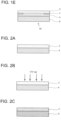
Fig. 1E is an illustrative drawing of the step (C) of the method of manufacturing an image display apparatus according to the present invention. -
Fig. 2A is an illustrative drawing of a step (AA) of the method of manufacturing an image display apparatus according to the present invention. -
Fig. 2B is an illustrative drawing of a step (BB) of the method of manufacturing an image display apparatus according to the present invention. -
Fig. 2C is an illustrative drawing of a step (BB) of the method of manufacturing an image display apparatus according to the present invention. -
Fig. 2D is an illustrative drawing of a step (CC) of the method of manufacturing an image display apparatus according to the present invention. -
Fig. 3 is an illustrative drawing of the evaluation test on the adhesion state of the light-transmissive cured resin layer. -
Fig. 4A is an illustrative drawing of an embodiment of coating of the light-transmissive cover member with the photocurable resin composition. -
Fig. 4B is an illustrative drawing of an embodiment of coating of the light-transmissive cover member with the photocurable resin composition. -
Fig. 5 is an illustrative drawing of an embodiment of coating of the light-transmissive cover member with the photocurable resin composition. -
Fig. 6 is an illustrative drawing of an embodiment of coating of the light-transmissive cover member with the photocurable resin composition. - Hereinafter, the method of manufacturing an image display apparatus according to the present invention, which includes the steps (A) to (C), will be described in detail for each step with reference to the drawings.
- First, as shown in
Fig. 1A , a light-transmissive cover member 2 including alight shielding layer 1 formed around an outer edge of one surface thereof is prepared. Next, as shown inFig. 1B , asurface 2a of the light-transmissive cover member 2 is coated with a liquidphotocurable resin composition 3 in a thickness thicker than that of thelight shielding layer 1 so that astep 4 formed by thelight shielding layer 1 and the light shielding layer formation-side surface 2a of the light-transmissive cover member 2 is canceled. Specifically, the whole of the light shielding layer formation-side surface 2a of the light-transmissive cover member 2, including the surface of thelight shielding layer 1, is coated flat with thephotocurable resin composition 3 so that a step does not occur. Therefore, thephotocurable resin composition 3 is coated in a thickness of preferably 1.2 to 50 times, and more preferably 2 to 30 times the thickness of thelight shielding layer 1. - The
photocurable resin composition 3 may be coated a plurality of times to obtain a required thickness. - The light-
transmissive cover member 2 has a light transmittance which allows an image formed on the image display member to be visually recognized. Examples of the light-transmissive cover member 2 may include a plate-like material and a sheet-like material of glass, an acrylic resin, polyethylene terephthalate, polyethylene naphthalate, and polycarbonate. These materials may be subjected to a single or double sided hard coating treatment, an antireflection treatment and the like. The physical properties such as a thickness and an elasticity of the light-transmissive cover member 2 can be determined depending on the intended use. - The
light shielding layer 1 is provided for, for example, enhancing the contrast of an image, and is obtained by performing coating with a paint colored in black or the like by a screen printing method or the like, and then drying and curing the coat. The thickness of thelight shielding layer 1 is usually 5 to 100 µm, which corresponds to the thickness of thestep 4. - The property of the
photocurable resin composition 3 used in this step is liquid. By using a liquid, thestep 4 formed by thelight shielding layer 1 and the light shielding layer formation-side surface 2a of the light-transmissive cover member 2 can be canceled. Here, a liquid indicates a substance having a viscosity of 0.01 to 100 Pa·s (at 25°C, cone-plate rheometer, cone and plate C35/2,rotational speed 10 rpm). - Examples of such a
photocurable resin composition 3 may include a substance which contains, for example, a radical photopolymerizable poly(meth)acrylate such as polyurethane-based (meth)acrylate and polyisoprene-based (meth)acrylate, and a photopolymerization initiator, as main ingredients. Here, the term "(meth)acrylate" means to include acrylate and methacrylate. - Preferred examples of the radical photopolymerizable poly(meth)acrylate may include a (meth)acrylate-based oligomer having polyisoprene, polybutadiene or polyurethane as a backbone.
- Preferred examples of the (meth)acrylate-based oligomer having a polyisoprene backbone may include an esterified product of a maleic anhydride adduct of a polyisoprene polymer and 2-hydroxyethyl methacrylate (UC102 (polystyrene-equivalent molecular weight: 17000), Kuraray Co., Ltd.; UC203 (polystyrene-equivalent molecular weight: 35000), Kuraray Co., Ltd.; UC-1 (molecular weight: approximately 25000), Kuraray Co., Ltd.).
- Preferred examples of the (meth)acrylate-based oligomer having a polyurethane backbone may include an aliphatic urethane acrylate (EBECRYL 230 (molecular weight: 5000), DAICEL-ALLNEX Ltd.; UA-1, Light Chemical Industries Co., Ltd.).
- As the photopolymerization initiator, publicly known radical photopolymerization initiators can be used. Examples thereof may include 1-hydroxy-cyclohexyl phenyl ketone (Irgacure 184, BASF Japan Ltd.), 2-hydroxy-1-{4-[4-(2-hydroxy-2-methyl-propionyl)benzyl]phenyl}-2-methyl-1-propan-1-one (Irgacure 127, BASF Japan Ltd.), benzophenone and acetophenone.
- When the amount of the photopolymerization initiator based on 100 parts by mass of radical photopolymerizable poly(meth)acrylate is too small, curing during UV irradiation becomes insufficient. When the amount is too large, an increase of an outgas due to cleavage tends to cause a foaming failure. Therefore, the amount of the photopolymerization initiator is preferably 0.1 to 5 parts by mass, and more preferably 0.2 to 3 parts by mass.
- The liquid
photocurable resin composition 3 may further contain publicly known plasticizers (flexibility-imparting agents) which are compatible with the radical photopolymerizable poly(meth)acrylate. Examples of such plasticizers may include a terpene-based hydrogenated resin, polybutadiene and polyisoprene. These plasticizers may also be used as a tackifier as described later. - The
photocurable resin composition 3 may also contain a reactive diluent. Preferred examples of the reactive diluent may include 2-hydroxypropyl methacrylate, benzyl acrylate and dicyclopentenyloxyethyl methacrylate. - The
photocurable resin composition 3 may further contain, as necessary, general additives, for example, an adhesion-improving agent such as a silane coupling agent, and an antioxidant. - The
photocurable resin composition 3 may also contain a chain transfer agent for adjusting a molecular weight. Examples of the chain transfer agent may include 2-mercapto ethanol, lauryl mercaptan, glycidyl mercaptan, mercaptoacetic acid, 2-ethylhexyl thioglycolate, 2,3-dimethylcapto-1-propanol and α-methylstyrene dimer. - It is noted that the UV irradiation in the step (B) described later can function, in some cases, such that the initial adhesive strength (a so-called tackiness) of the
photocurable resin composition 3 is decreased, and the final adhesive strength is reduced. Therefore, a so-called tackifier is desirably mixed in thephotocurable resin composition 3. Examples of the tackifier used may include terpene-based resins such as a terpene resin, a terpene phenol resin and a hydrogenated terpene resin; rosin resins such as a natural rosin, a polymerized rosin, a rosin ester and a hydrogenated rosin; and petroleum resins such as polybutadiene and polyisoprene. The mixed amount of such a tackifier in 100 parts by mass of the photocurable resin composition is preferably 40 to 70 parts by mass. - Although the base material of the
photocurable resin composition 3 is the above-described radical photopolymerizable poly(meth)acrylate, the radical photopolymerizable poly(meth)acrylate which has been previously polymerized can be contained as the base material in order to develop the tackiness-imparting effect of the tackifier more strongly. Examples of such a polymerized material may include a copolymer of butyl acrylate and 2-hexyl acrylate, and an acrylic acid; and a copolymer of cyclohexyl acrylate and a methacrylic acid. - Next, as shown in
Fig. 1C , UV rays are irradiated to the coat of thephotocurable resin composition 3 formed in the step (A) for curing to form a light-transmissive cured resin layer 5 (Fig. 1D ). By the curing, the light-transmissive curedresin layer 5 between thelight shielding layer 1 and theimage display member 6 can be sufficiently photocured without being excessively eliminated from between thelight shielding layer 1 and the image display member. The level of the curing is such that the curing rate (gel fraction) of the light-transmissive curedresin layer 5 is preferably 90% or more, and further preferably 95% or more. Here, the curing rate (gel fraction) is a value defined as a ratio (consumption ratio) of the present amount of a (meth)acryloyl group after UV irradiation to the present amount of a (meth)acryloyl group before UV irradiation in thephotocurable resin composition 3. The larger this value is, the further the curing proceeds. - The curing rate (gel fraction) can be calculated by substituting in a mathematical expression (1) below an absorption peak height (X) from the baseline at 1640 to 1620 cm-1 in the FT-IR measurement chart of the resin composition layer before UV irradiation, and an absorption peak height (Y) from the baseline at 1640 to 1620 cm-1 in the FT-IR measurement chart of the resin composition layer after UV irradiation.

- Regarding UV irradiation, the type, output and accumulated light amount of a light source are not particularly limited as long as the curing can be performed so as to have a curing rate (gel fraction) of preferably 90% or more, and a publicly known process condition for radically photopolymerizing (meth)acrylate with UV irradiation can be adopted.
- Next, as shown in
Fig. 1E , the light-transmissive cover member 2 is bonded to animage display member 6 on the side of the light-transmissive curedresin layer 5. The bonding can be performed under pressure at 10°C to 80°C using a publicly known pressure bonding apparatus. Accordingly, theimage display member 6 and the light-transmissive cover member 2 are laminated to each other via the light-transmissive curedresin layer 5 to obtain animage display apparatus 10. - Examples of the
image display member 6 may include a liquid crystal display panel, an organic EL display panel, a plasma display panel and a touch panel. Here, the touch panel means an image display and input panel in which a display element such as a liquid crystal display panel and a position input device such as a touch pad are combined. - The light transmittance level of the light-transmissive cured
resin layer 5 may be such that an image formed on theimage display member 6 can be visually recognized. - Although an example in which the photocurable resin composition is coated on the light shielding layer-side surface of the light-transmissive cover member has been described in
Fig. 1A to Fig. 1E , an example in which the photocurable resin composition is coated on the surface of the image display member will be described inFig. 2A to Fig. 2D below. The same reference numerals assigned inFig. 1A to Fig. 1E and inFig. 2A to Fig. 2D represent the same components. - First, as shown in
Fig. 2A , thephotocurable resin composition 3 is coated flat on the surface of theimage display member 6. The coated thickness in this case is preferably 1.2 to 50 times, and further preferably 2 to 30 times the thickness of the light shielding layer so that the step formed by the light shielding layer and the light shielding layer formation-side surface of the light-transmissive cover member is canceled. - The coating of the
photocurable resin composition 3 may be performed a plurality of times to obtain a necessary thickness. - Next, as shown in
Fig. 2B , UV rays are irradiated to thephotocurable resin composition 3 coated in the step (AA) for curing to form the light-transmissive cured resin layer 5 (Fig. 2C ). By curing the composition in this manner, the light-transmissive curedresin layer 5 between the light shielding layer and the image display member can be sufficiently photocured without being eliminated from between thelight shielding layer 1 and theimage display member 6. The level of the curing is such that the gel fraction of the light-transmissive curedresin layer 5 is preferably 90% or more, and more preferably 95% or more. - Next, as shown in
Fig. 2D , the light-transmissive cover member 2 is bonded to the light-transmissive curedresin layer 5 of theimage display member 6 on the side of thelight shielding layer 1. The bonding can be performed under pressure at 10 to 80°C using a publicly known pressure bonding apparatus. Accordingly, theimage display member 6 and the light-transmissive cover member 2 are laminated to each other via the light-transmissive curedresin layer 5 to obtain theimage display apparatus 10. - Examples of the
image display member 6 may include a liquid crystal display panel, an organic EL display panel, a plasma display panel and a touch panel. - The light transmittance level of the light-transmissive cured
resin layer 5 may be such that an image formed on theimage display member 6 can be visually recognized. - The present invention further relates to the following items.
- 1. A method of manufacturing an image display apparatus wherein an image display member and a light-transmissive cover member having a light shielding layer formed around an outer edge of the cover member are laminated to each other via a light-transmissive cured resin layer formed from a liquid photocurable resin composition such that a surface of the light-transmissive cover member on which the light shielding layer is formed is arranged on a side of the image display member, the manufacturing method comprising the following steps (A) to (C) :
- <Step (A) >
coating the surface of the light-transmissive cover member on which the light shielding layer is formed or the surface of the image display member with the liquid photocurable resin composition in a thickness thicker than that of the light shielding layer so that a step formed by the light shielding layer and the surface of the light-transmissive cover member on which the light shielding layer is formed is canceled; - <Step (B) >
irradiating UV rays to the coated photocurable resin composition for curing to form a light-transmissive cured resin layer; and - <Step (C)>
bonding the light-transmissive cover member with the image display member such that the light shielding layer and the light-transmissive cured resin layer are located inside.
- <Step (A) >
- 2. The manufacturing method according to item 1., wherein the image display member is a liquid crystal display panel, an organic EL display panel or a touch panel.
- 3. The manufacturing method according to
item 1. or 2., wherein in the step (A), the photocurable resin composition is coated in a thickness 1.2 to 50 times a thickness of the light shielding layer. - 4. The manufacturing method according to any of
items 1. to 3., wherein in the step (B), the photocurable resin composition is irradiated with UV rays for curing so that the light-transmissive cured resin layer has a curing rate of 90% or more. - 5. The manufacturing method according to any of
items 1. to 4., wherein the liquid photocurable resin composition contains polyurethane-based (meth)acrylate or polyisoprene-based (meth)acrylate, and a photopolymerization initiator. - The present invention will be specifically described by way of examples below.
- First, a glass plate having a size of 45 (w) × 80 (1) × 0.4 (t) mm was prepared. An entire region of the outer edge of the glass plate was coated with a photocurable black ink (MRX Ink, Teikoku Printing Inks Mfg. Co., Ltd) by a screen printing method so as to form a light shielding layer having a dry thickness of 40 µm and a width of 4 mm. The coated black ink was dried to prepare a glass plate with a light shielding layer.
- Also, 6 parts by weight of polyisoprene methacrylate (UC102, Kuraray Co., Ltd.) as a radical photopolymerizable poly(meth)acrylate, 15 parts by weight of dicyclopentenyloxyethyl methacrylate and 5 parts by weight of lauryl methacrylate as a reactive diluent, 20 parts by weight of polybutadiene (Polyvest 110, Evonik Japan Co., Ltd.) as a plasticizer, 1 part by weight of a photopolymerization initiator (Irgacure 184, BASF Japan Ltd.) and 53 parts by weight of a hydrogenated terpene resin (Clearon M105, Yasuhara Chemical Co., Ltd.) as a tackifier were uniformly mixed to prepare a photocurable resin composition. The viscosity (cone-plate rheometer, 25°C, cone and plate C35/2,
rotational speed 10 rpm) of this photocurable resin composition was approximately 6 Pa·s. - Next, the photocurable resin composition was discharged on the entire light shielding layer-formed surface of the glass plate including the light shielding layer with a resin dispenser to form a photocurable resin composition film having an average thickness of 200 µm. The photocurable resin composition film was formed so as to be substantially spread over the entire region of the light shielding layer as shown in
Fig. 1B in a thickness thicker by 160 µm than the light shielding layer having a thickness of 40 µm. - Next, the photocurable resin composition film was irradiated with UV rays having an intensity of 50 mW/cm2 for 60 seconds so that the accumulated light amount becomes 3000 mJ/cm2, using a UV irradiation device (LC-8, Hamamatsu Photonics K.K.), to cure the photocurable resin composition film. In this manner, a light-transmissive cured resin layer was formed.
- The photocurable resin composition film after UV irradiation, that is the light-transmissive cured resin layer, had a curing rate of approximately 92%. The curing rate was calculated by using as an index an absorption peak height from the baseline at 1640 to 1620 cm-1 in the FT-IR measurement chart.
- Furthermore, the tackiness of the surface of the light-transmissive cured resin layer was 110 N/cm2, based on a measurement by a probe tack method using a tacking tester (TAC-II, Rhesca Co., Ltd.).
- Next, the glass plate obtained in the step (B) was placed on the surface of a laminated polarizing plate of a liquid crystal display element having a size of 40 (W) × 70 (L) mm so that the light-transmissive cured resin layer side of the glass plate is on the polarizing plate side. Then, pressure was applied from the glass plate side with a rubber roller so that the glass plate was bonded to the liquid crystal display element. When the bonded liquid crystal display element was visually observed from the glass plate side, air bubbles were not observed around the light shielding layer.
- The product obtained in each of the steps in Example 1 was visually observed on whether or not air bubbles exist in the boundary between the light shielding layer and the photocurable resin composition film layer or the light-transmissive cured resin layer, as will be described below. In addition, the adhesion state of the liquid crystal display apparatus was evaluated as will be described below.
- The product obtained in each of the steps in Example 1 was visually observed on whether or not air bubbles exist in the boundary between the light shielding layer and the photocurable resin composition film layer or the cured resin layer. As a result, air bubbles were not observed in the product obtained in any of the steps and in the final liquid crystal display apparatus.
- When preparing a liquid crystal display apparatus, a
glass base 30 having a size of 40 (W) × 70 (L) mm was used instead of a liquid crystal display element. Aglass plate 31 including a light-transmissive cured resin layer formed thereon was bonded to theglass base 30 on the light-transmissive cured resin layer side into a cross shape. Thus, a glass connection body was obtained. Then, while theglass base 30 positioned on the lower side of the connection body was fixed, theglass plate 31 positioned on the upper side was peeled off directly upward. Then, the peeling property was visually observed, and the adhesion state was evaluated as "A" in accordance with the criteria below. -
- A: When aggregation peeling occurred
- B: When both aggregation peeling and interface peeling existed
- C: When interface peeling occurred
- A liquid crystal display apparatus and a glass connection body for measuring an adhesion strength were prepared in the same manner as in Example 1, except that in the step (A) (Coating step) of Example 1, the photocurable resin composition film was formed so as to be spread over approximately 70% of the width of the light shielding layer. Then, observation was performed on whether or not air bubbles exist, and the adhesion state was evaluated. As a result, even when the photocurable resin composition film was formed to be spread over approximately 70% of the width of the light shielding layer, air bubbles did not exist in the product obtained in each step and in the final liquid crystal display apparatus in Example 2, and the adhesion state was also evaluated as "A."
- A liquid crystal display apparatus and a glass connection body for measuring an adhesion strength were prepared in the same manner as in Example 1, except that in the step (A) (Coating step) of Example 1, the photocurable resin composition film formed had a thickness of approximately 1.2 times the thickness of the light shielding layer. Then, observation was performed on whether or not air bubbles exist, and the adhesion state was evaluated. As a result, when the photocurable resin composition film formed had a thickness of approximately 1.2 times the thickness of the light shielding layer, air bubbles did not exist in the product obtained in each step and in the final liquid crystal display apparatus in Example 3, and the adhesion state was also evaluated as "A."
- A liquid crystal display apparatus and a glass connection body for measuring an adhesion strength were prepared in the same manner as in Example 1, except that in the step (A) (Coating step) of Example 1, as shown in
Fig. 4A , aphotocurable resin composition 3a was coated in the same thickness as that of thelight shielding layer 1 without being spread over thelight shielding layer 1, and further, as shown inFig. 4B , aphotocurable resin composition 3b was coated so as to be spread over thelight shielding layer 1. Then, observation was performed on whether or not air bubbles exist, and the adhesion state was evaluated. As a result, even when the photocurable resin composition was multi-layered, air bubbles did not exist in the product obtained in each step and in the final liquid crystal display apparatus in Example 4, and the adhesion state was also evaluated as "A." - A liquid crystal display apparatus and a glass connection body for measuring an adhesion strength were prepared in the same manner as in Example 1, except that in the step (A) (Coating: step) of Example 1, the
photocurable resin composition 3 was spread over an entire region of thelight shielding layer 1, but had a thickness of 30 µm thinner than that of thelight shielding layer 1, as shown inFig. 5 . Then, observation was performed on whether or not air bubbles exist, and the adhesion state was evaluated. As a result, although air bubbles were not observed in the product obtained in the step (A), air bubbles were observed in the product obtained in the step (C). The adhesion state was also evaluated as "A." - A liquid crystal display apparatus and a glass connection body for measuring an adhesion strength were prepared in the same manner as in Example 1, except that in the step (A) (Coating step) of Example 1, as shown in
Fig. 6 , thephotocurable resin composition 3 was not formed so as to be spread over thelight shielding layer 1, and was coated thinner than thelight shielding layer 1. Then, observation was performed on whether or not air bubbles exist, and the adhesion state was evaluated. As a result, although air bubbles were not found in the product obtained in the step (A), air bubbles were found in the product obtained in the bonding step of the step (C). The adhesion state was also evaluated as "A." - A liquid crystal display apparatus and a glass connection body for measuring an adhesion strength were prepared in the same manner as in Example 1, except that in the step (A) of Example 1, the photocurable resin composition was not coated on the glass plate, but formed on a release film; UV irradiation similar to the step (B) of Example 1 was performed to form a light-transmissive cured resin layer of the photocurable resin composition on the release film ; and the light-transmissive cured resin layer was transferred on the glass plate including the light shielding layer formed thereon. Then, observation was performed on whether or not air bubbles exist, and the adhesion state was evaluated. As a result, air bubbles were found around the step of the light shielding layer when the light-transmissive cured resin layer was transferred. Air bubbles were also observed in the product obtained in the following step (C). The adhesion state was evaluated as "B."
- According to the method of manufacturing an image display apparatus of the present invention, the light-transmissive cured resin layer between the light shielding layer and the image display member can be sufficiently photocured without being excessively eliminated from between the light shielding layer and the image display member. Furthermore, the step formed between the light shielding layer and the light shielding layer formation-side surface of the light-transmissive cover member can be canceled. Therefore, the manufacturing method according to the present invention is useful in industrial manufacturing of information terminals such as a smartphone equipped with a touch panel, and a touch pad.
-
- 1
- Light shielding layer
- 2
- Light-transmissive cover member
- 2a
- (Light shielding layer formation-side) surface of light-transmissive cover member
- 3, 3a, 3b
- Photocurable resin composition
- 4
- Step
- 5
- Light-transmissive cured resin layer
- 6
- Image display member
- 10
- Image display apparatus
- 30
- Glass base
- 31
- Glass plate
Claims (5)
- A method of manufacturing an image display apparatus (10) wherein an image display member (6) and a light-transmissive cover member (2) having a light shielding layer (1) formed around an outer edge of the cover member (2) are laminated to each other via a light-transmissive cured resin layer (5) formed from a liquid photocurable resin composition (3, 3a, 3b) such that a surface (2a) of the light-transmissive cover member (2) on which the light shielding layer (1) is formed is arranged on a side of the image display member (6), the manufacturing method comprising the following steps (A) to (C) :<Step (A) >
coating the surface (2a) of the light-transmissive cover member (2) on which the light shielding layer (1) is formed with the liquid photocurable resin composition (3, 3a, 3b) in a thickness thicker than that of the light shielding layer (1) so that a step (4) formed by the light shielding layer (1) and the surface (2a) of the light-transmissive cover member (2) on which the light shielding layer (1) is formed is canceled, wherein the liquid photocurable resin composition (3, 3a, 3b) has a viscosity of 0.01 to 100 Pa·s and is coated in a thickness 2 to 30 times a thickness of the light shielding layer (1);<Step (B) >
irradiating UV rays to the coated photocurable resin composition (3, 3a, 3b) for curing to form a light-transmissive cured resin layer (5); and<Step (C)>
bonding the light-transmissive cover member (2) with the image display member (6) under pressure at 10°C to 80°C using a publicly known pressure bonding apparatus such that the light shielding layer (1) and the light-transmissive cured resin layer (5) are located inside. - The manufacturing method according to claim 1, wherein the image display member (6) is a liquid crystal display panel, an organic EL display panel or a touch panel.
- The manufacturing method according to claim 1 or 2, wherein in the step (B), the photocurable resin composition (3, 3a, 3b) is irradiated with UV rays for curing so that the light-transmissive cured resin layer (5) has a curing rate of 90% or more.
- The manufacturing method according to any of claims 1 to 3, wherein the liquid photocurable resin composition (3, 3a, 3b) contains polyurethane-based (meth)acrylate or polyisoprene-based (meth)acrylate, and a photopolymerization initiator.
- The manufacturing method according to any of claims 1 to 4, wherein in the step (A), the whole of the surface (2a) of the light-transmissive cover member (2) on which the light shielding layer (1) is formed, including the surface of the light shielding layer (1), is coated with the liquid photocurable resin composition (3, 3a, 3b) in a thickness thicker than that of the light shielding layer (1) so that a step (4) formed by the light shielding layer (1) and the surface (2a) of the light-transmissive cover member (2) on which the light shielding layer (1) is formed is canceled.
Applications Claiming Priority (3)
| Application Number | Priority Date | Filing Date | Title |
|---|---|---|---|
| JP2012107707 | 2012-05-09 | ||
| EP13788012.6A EP2849170B1 (en) | 2012-05-09 | 2013-04-30 | Image display device manufacturing method |
| PCT/JP2013/062552 WO2013168629A1 (en) | 2012-05-09 | 2013-04-30 | Image display device manufacturing method |
Related Parent Applications (1)
| Application Number | Title | Priority Date | Filing Date |
|---|---|---|---|
| EP13788012.6A Division EP2849170B1 (en) | 2012-05-09 | 2013-04-30 | Image display device manufacturing method |
Publications (2)
| Publication Number | Publication Date |
|---|---|
| EP4184485A1 true EP4184485A1 (en) | 2023-05-24 |
| EP4184485B1 EP4184485B1 (en) | 2025-08-13 |
Family
ID=49550671
Family Applications (2)
| Application Number | Title | Priority Date | Filing Date |
|---|---|---|---|
| EP22215388.4A Active EP4184485B1 (en) | 2012-05-09 | 2013-04-30 | Method of manufacturing image display apparatus |
| EP13788012.6A Active EP2849170B1 (en) | 2012-05-09 | 2013-04-30 | Image display device manufacturing method |
Family Applications After (1)
| Application Number | Title | Priority Date | Filing Date |
|---|---|---|---|
| EP13788012.6A Active EP2849170B1 (en) | 2012-05-09 | 2013-04-30 | Image display device manufacturing method |
Country Status (9)
| Country | Link |
|---|---|
| US (3) | US9718264B2 (en) |
| EP (2) | EP4184485B1 (en) |
| JP (2) | JP5477495B2 (en) |
| KR (2) | KR101791731B1 (en) |
| CN (2) | CN104272370B (en) |
| HK (1) | HK1202696A1 (en) |
| HU (2) | HUE073469T2 (en) |
| TW (1) | TWI501002B (en) |
| WO (1) | WO2013168629A1 (en) |
Families Citing this family (9)
| Publication number | Priority date | Publication date | Assignee | Title |
|---|---|---|---|---|
| JP5304922B1 (en) * | 2012-05-09 | 2013-10-02 | デクセリアルズ株式会社 | Manufacturing method of image display device |
| CN104272370B (en) | 2012-05-09 | 2016-12-07 | 迪睿合电子材料有限公司 | Method for manufacturing image display device |
| KR20150097359A (en) | 2014-02-18 | 2015-08-26 | 주식회사 엘지화학 | Encapsulation film and organic electronic device comprising the same |
| JP5901808B2 (en) | 2014-08-05 | 2016-04-13 | 古河電気工業株式会社 | Curable hygroscopic resin composition for sealing electronic device, sealing resin and electronic device |
| JP6273193B2 (en) * | 2014-11-20 | 2018-01-31 | 協立化学産業株式会社 | Manufacturing method of laminate |
| JP6948776B2 (en) * | 2016-10-12 | 2021-10-13 | 昭和電工パッケージング株式会社 | Manufacturing method of packaging material |
| JP2019191560A (en) * | 2018-04-24 | 2019-10-31 | 住友化学株式会社 | Optical laminate and manufacturing method thereof |
| JP2026050264A (en) * | 2024-09-09 | 2026-03-19 | デクセリアルズ株式会社 | Image display device and method for manufacturing an image display device |
| JP2026050265A (en) * | 2024-09-09 | 2026-03-19 | デクセリアルズ株式会社 | Image display device and method for manufacturing an image display device |
Citations (5)
| Publication number | Priority date | Publication date | Assignee | Title |
|---|---|---|---|---|
| US6995193B1 (en) * | 2000-02-14 | 2006-02-07 | Sekisui Chemical Co., Ltd. | Photocurable composition, process for producing photocurable composition, photocurable pressure-sensitive adhesive sheet, process for producing photocurable pressure-sensitive adhesive sheet, and method of bonding |
| WO2008126860A1 (en) | 2007-04-09 | 2008-10-23 | Sony Chemical & Information Device Corporation | Image display device, resin composition, resin cured layer and method for manufacturing image display device |
| JP2009186954A (en) * | 2007-04-04 | 2009-08-20 | Sony Chemical & Information Device Corp | Method of manufacturing image display apparatus |
| KR100945381B1 (en) * | 2009-07-01 | 2010-03-08 | 강용호 | Icon sheet for display window of mobile apparatus and method of the same, display window for mobile apparatus and mobile apparatus including the same |
| WO2010027041A1 (en) | 2008-09-05 | 2010-03-11 | 協立化学産業株式会社 | Photocurable resin composition for laminating optically functional material |
Family Cites Families (38)
| Publication number | Priority date | Publication date | Assignee | Title |
|---|---|---|---|---|
| US5747551A (en) * | 1994-12-05 | 1998-05-05 | Acheson Industries, Inc. | UV curable pressure sensitive adhesive composition |
| US6649259B1 (en) * | 2000-02-29 | 2003-11-18 | National Starch And Chemical Investment Holding Corporation | Adhesives for thermally shrinkable films or labels |
| JP2002341320A (en) * | 2001-05-15 | 2002-11-27 | Fuji Photo Film Co Ltd | Liquid crystal display device and optical laminate |
| JP4134559B2 (en) * | 2002-01-15 | 2008-08-20 | 岩崎電気株式会社 | Hardener for sealing material of glass substrate for display panel |
| JP4150534B2 (en) | 2002-05-22 | 2008-09-17 | シャープ株式会社 | Manufacturing method of display element |
| WO2003099912A1 (en) * | 2002-05-27 | 2003-12-04 | Nitto Denko Corporation | Resin sheet and liquid-crystal cell substrate comprising the same |
| JP2005107199A (en) * | 2003-09-30 | 2005-04-21 | Dainippon Printing Co Ltd | Optical filter and plasma display panel |
| EP1674505B1 (en) * | 2003-10-07 | 2011-12-07 | Bridgestone Corporation | Photocuring transfer sheet, method for manufacturing optical information recording medium using the sheet, and optical information recording medium |
| US7285313B2 (en) * | 2004-01-20 | 2007-10-23 | Lg Chem Ltd. | Acrylic pressure-sensitive adhesive composition for polarizing film |
| US7238732B2 (en) * | 2004-02-18 | 2007-07-03 | Eastman Chemical Company | Radiation-curable adhesive compositions |
| KR101253802B1 (en) * | 2005-12-05 | 2013-04-12 | 세이코 인스트루 가부시키가이샤 | Display and method for manufacturing display |
| KR100932887B1 (en) * | 2005-12-14 | 2009-12-21 | 주식회사 엘지화학 | Acrylic pressure-sensitive adhesive composition |
| EP3118841B1 (en) * | 2006-07-14 | 2021-01-06 | Dexerials Corporation | Resin composition and display apparatus |
| CN101426648A (en) * | 2006-12-30 | 2009-05-06 | Mogem有限公司 | Window for display device, manufacturing method thereof and wireless terminal unit comprising the same |
| CN101652803B (en) * | 2007-04-03 | 2015-02-04 | 迪睿合电子材料有限公司 | Method for manufacturing image display device |
| KR101527980B1 (en) * | 2007-04-03 | 2015-06-10 | 데쿠세리아루즈 가부시키가이샤 | Manufacturing method of image display device |
| WO2008123611A1 (en) * | 2007-04-04 | 2008-10-16 | Sony Chemical & Information Device Corporation | Method for manufacturing image display |
| JP5401824B2 (en) * | 2007-04-09 | 2014-01-29 | デクセリアルズ株式会社 | Image display device |
| CN101285969B (en) * | 2007-04-13 | 2012-07-04 | 群康科技(深圳)有限公司 | Liquid crystal display panel and method for producing same |
| JP2008266473A (en) * | 2007-04-20 | 2008-11-06 | Nitto Denko Corp | Transparent adhesive sheet and flat panel display |
| JP2009008973A (en) * | 2007-06-29 | 2009-01-15 | Hitachi Displays Ltd | Liquid crystal display |
| JP4711354B2 (en) * | 2007-07-17 | 2011-06-29 | ソニーケミカル&インフォメーションデバイス株式会社 | Manufacturing method of image display device |
| JP5343391B2 (en) * | 2007-07-17 | 2013-11-13 | デクセリアルズ株式会社 | Resin composition and image display device |
| JP5288753B2 (en) * | 2007-09-07 | 2013-09-11 | 新光電気工業株式会社 | Method and apparatus for laminating UV curable waveguide material |
| US20100277684A1 (en) * | 2007-10-22 | 2010-11-04 | Hiroshi Fukushima | Display device and method for production thereof |
| CN101645363A (en) * | 2008-08-04 | 2010-02-10 | 钟金龙 | Continuous forming method of film type keyboard group unit |
| JP2010072471A (en) * | 2008-09-19 | 2010-04-02 | Three M Innovative Properties Co | Transparent adhesive sheet, image display apparatus comprising the same, and method for producing the image display apparatus |
| TWI373665B (en) * | 2008-12-25 | 2012-10-01 | Au Optronics Corp | Touch panel structure |
| JP5545296B2 (en) * | 2009-07-22 | 2014-07-09 | 日立化成株式会社 | Photo-curable resin composition and cured product thereof, resin sheet and production method thereof, and display device |
| JP4992958B2 (en) * | 2009-11-30 | 2012-08-08 | カシオ計算機株式会社 | Manufacturing method of plate member assembly and manufacturing method of electronic member with transparent substrate |
| JP5605088B2 (en) | 2009-12-03 | 2014-10-15 | ソニー株式会社 | Liquid crystal display |
| CN102792218B (en) * | 2010-03-09 | 2016-02-03 | 3M创新有限公司 | For bonding the thermal activation optically clear adhesive of display panel |
| CN104698658A (en) * | 2010-05-26 | 2015-06-10 | 旭硝子株式会社 | Transparent surface material having adhesive layer, display device, and manufacturing method for same |
| JP5750848B2 (en) * | 2010-08-26 | 2015-07-22 | 住友化学株式会社 | Optical member for image display device |
| JP5558993B2 (en) | 2010-09-29 | 2014-07-23 | 芝浦メカトロニクス株式会社 | Adhesive supply device and adhesive supply method |
| CN105842894B (en) * | 2012-01-25 | 2020-09-22 | 迪睿合电子材料有限公司 | Manufacturing method of image display device |
| CN104272370B (en) | 2012-05-09 | 2016-12-07 | 迪睿合电子材料有限公司 | Method for manufacturing image display device |
| JP5370706B1 (en) | 2012-12-14 | 2013-12-18 | デクセリアルズ株式会社 | Manufacturing method of image display device |
-
2013
- 2013-04-30 CN CN201380002824.6A patent/CN104272370B/en active Active
- 2013-04-30 EP EP22215388.4A patent/EP4184485B1/en active Active
- 2013-04-30 HK HK15102554.7A patent/HK1202696A1/en unknown
- 2013-04-30 HU HUE22215388A patent/HUE073469T2/en unknown
- 2013-04-30 CN CN201610979393.4A patent/CN106896551B/en active Active
- 2013-04-30 WO PCT/JP2013/062552 patent/WO2013168629A1/en not_active Ceased
- 2013-04-30 HU HUE13788012A patent/HUE060772T2/en unknown
- 2013-04-30 US US14/353,900 patent/US9718264B2/en active Active
- 2013-04-30 KR KR1020147005040A patent/KR101791731B1/en active Active
- 2013-04-30 JP JP2013095061A patent/JP5477495B2/en active Active
- 2013-04-30 EP EP13788012.6A patent/EP2849170B1/en active Active
- 2013-04-30 KR KR1020177008687A patent/KR101962550B1/en active Active
- 2013-05-09 TW TW102116497A patent/TWI501002B/en active
-
2014
- 2014-02-12 JP JP2014024291A patent/JP6318671B2/en active Active
-
2017
- 2017-06-22 US US15/630,347 patent/US10882293B2/en active Active
-
2020
- 2020-12-22 US US17/130,090 patent/US11945203B2/en active Active
Patent Citations (5)
| Publication number | Priority date | Publication date | Assignee | Title |
|---|---|---|---|---|
| US6995193B1 (en) * | 2000-02-14 | 2006-02-07 | Sekisui Chemical Co., Ltd. | Photocurable composition, process for producing photocurable composition, photocurable pressure-sensitive adhesive sheet, process for producing photocurable pressure-sensitive adhesive sheet, and method of bonding |
| JP2009186954A (en) * | 2007-04-04 | 2009-08-20 | Sony Chemical & Information Device Corp | Method of manufacturing image display apparatus |
| WO2008126860A1 (en) | 2007-04-09 | 2008-10-23 | Sony Chemical & Information Device Corporation | Image display device, resin composition, resin cured layer and method for manufacturing image display device |
| WO2010027041A1 (en) | 2008-09-05 | 2010-03-11 | 協立化学産業株式会社 | Photocurable resin composition for laminating optically functional material |
| KR100945381B1 (en) * | 2009-07-01 | 2010-03-08 | 강용호 | Icon sheet for display window of mobile apparatus and method of the same, display window for mobile apparatus and mobile apparatus including the same |
Also Published As
| Publication number | Publication date |
|---|---|
| WO2013168629A1 (en) | 2013-11-14 |
| KR101962550B1 (en) | 2019-03-26 |
| US20140305582A1 (en) | 2014-10-16 |
| US10882293B2 (en) | 2021-01-05 |
| KR20140042918A (en) | 2014-04-07 |
| CN104272370B (en) | 2016-12-07 |
| JP6318671B2 (en) | 2018-05-09 |
| JP2013254195A (en) | 2013-12-19 |
| EP2849170A1 (en) | 2015-03-18 |
| CN104272370A (en) | 2015-01-07 |
| US11945203B2 (en) | 2024-04-02 |
| KR101791731B1 (en) | 2017-10-30 |
| EP4184485B1 (en) | 2025-08-13 |
| CN106896551A (en) | 2017-06-27 |
| CN106896551B (en) | 2021-05-18 |
| US20170282530A1 (en) | 2017-10-05 |
| JP5477495B2 (en) | 2014-04-23 |
| TW201413339A (en) | 2014-04-01 |
| HUE073469T2 (en) | 2026-01-28 |
| HK1202696A1 (en) | 2015-10-02 |
| US9718264B2 (en) | 2017-08-01 |
| US20210107268A1 (en) | 2021-04-15 |
| HUE060772T2 (en) | 2023-04-28 |
| JP2014123144A (en) | 2014-07-03 |
| EP2849170A4 (en) | 2016-03-09 |
| KR20170038132A (en) | 2017-04-05 |
| TWI501002B (en) | 2015-09-21 |
| EP2849170B1 (en) | 2023-01-11 |
Similar Documents
| Publication | Publication Date | Title |
|---|---|---|
| US11945203B2 (en) | Method of manufacturing image display apparatus | |
| KR102137449B1 (en) | Method of manufacturing image display device | |
| JP5218802B1 (en) | Manufacturing method of image display device | |
| JP5138820B1 (en) | Manufacturing method of image display device | |
| EP2767970B1 (en) | Method for producing image display device | |
| JP5304960B1 (en) | Manufacturing method of image display device | |
| JP6220123B2 (en) | Manufacturing method of image display device | |
| JP2014081642A (en) | Method for manufacturing image display apparatus | |
| JP5440725B2 (en) | Manufacturing method of image display device | |
| JP6786647B2 (en) | Manufacturing method of image display device | |
| HK1191437B (en) | Image display device fabrication method |
Legal Events
| Date | Code | Title | Description |
|---|---|---|---|
| PUAI | Public reference made under article 153(3) epc to a published international application that has entered the european phase |
Free format text: ORIGINAL CODE: 0009012 |
|
| STAA | Information on the status of an ep patent application or granted ep patent |
Free format text: STATUS: THE APPLICATION HAS BEEN PUBLISHED |
|
| AC | Divisional application: reference to earlier application |
Ref document number: 2849170 Country of ref document: EP Kind code of ref document: P |
|
| AK | Designated contracting states |
Kind code of ref document: A1 Designated state(s): AL AT BE BG CH CY CZ DE DK EE ES FI FR GB GR HR HU IE IS IT LI LT LU LV MC MK MT NL NO PL PT RO RS SE SI SK SM TR |
|
| STAA | Information on the status of an ep patent application or granted ep patent |
Free format text: STATUS: REQUEST FOR EXAMINATION WAS MADE |
|
| 17P | Request for examination filed |
Effective date: 20231123 |
|
| RBV | Designated contracting states (corrected) |
Designated state(s): AL AT BE BG CH CY CZ DE DK EE ES FI FR GB GR HR HU IE IS IT LI LT LU LV MC MK MT NL NO PL PT RO RS SE SI SK SM TR |
|
| GRAP | Despatch of communication of intention to grant a patent |
Free format text: ORIGINAL CODE: EPIDOSNIGR1 |
|
| STAA | Information on the status of an ep patent application or granted ep patent |
Free format text: STATUS: GRANT OF PATENT IS INTENDED |
|
| INTG | Intention to grant announced |
Effective date: 20250306 |
|
| GRAS | Grant fee paid |
Free format text: ORIGINAL CODE: EPIDOSNIGR3 |
|
| GRAA | (expected) grant |
Free format text: ORIGINAL CODE: 0009210 |
|
| STAA | Information on the status of an ep patent application or granted ep patent |
Free format text: STATUS: THE PATENT HAS BEEN GRANTED |
|
| AC | Divisional application: reference to earlier application |
Ref document number: 2849170 Country of ref document: EP Kind code of ref document: P |
|
| AK | Designated contracting states |
Kind code of ref document: B1 Designated state(s): AL AT BE BG CH CY CZ DE DK EE ES FI FR GB GR HR HU IE IS IT LI LT LU LV MC MK MT NL NO PL PT RO RS SE SI SK SM TR |
|
| RAP3 | Party data changed (applicant data changed or rights of an application transferred) |
Owner name: DEXERIALS CORPORATION |
|
| REG | Reference to a national code |
Ref country code: GB Ref legal event code: FG4D |
|
| REG | Reference to a national code |
Ref country code: CH Ref legal event code: EP |
|
| REG | Reference to a national code |
Ref country code: DE Ref legal event code: R096 Ref document number: 602013086969 Country of ref document: DE |
|
| REG | Reference to a national code |
Ref country code: IE Ref legal event code: FG4D |
|
| REG | Reference to a national code |
Ref country code: NL Ref legal event code: MP Effective date: 20250813 |
|
| PG25 | Lapsed in a contracting state [announced via postgrant information from national office to epo] |
Ref country code: IS Free format text: LAPSE BECAUSE OF FAILURE TO SUBMIT A TRANSLATION OF THE DESCRIPTION OR TO PAY THE FEE WITHIN THE PRESCRIBED TIME-LIMIT Effective date: 20251213 |
|
| PG25 | Lapsed in a contracting state [announced via postgrant information from national office to epo] |
Ref country code: NO Free format text: LAPSE BECAUSE OF FAILURE TO SUBMIT A TRANSLATION OF THE DESCRIPTION OR TO PAY THE FEE WITHIN THE PRESCRIBED TIME-LIMIT Effective date: 20251113 |
|
| REG | Reference to a national code |
Ref country code: LT Ref legal event code: MG9D |
|
| PG25 | Lapsed in a contracting state [announced via postgrant information from national office to epo] |
Ref country code: PT Free format text: LAPSE BECAUSE OF FAILURE TO SUBMIT A TRANSLATION OF THE DESCRIPTION OR TO PAY THE FEE WITHIN THE PRESCRIBED TIME-LIMIT Effective date: 20251215 |
|
| PG25 | Lapsed in a contracting state [announced via postgrant information from national office to epo] |
Ref country code: FI Free format text: LAPSE BECAUSE OF FAILURE TO SUBMIT A TRANSLATION OF THE DESCRIPTION OR TO PAY THE FEE WITHIN THE PRESCRIBED TIME-LIMIT Effective date: 20250813 |
|
| PG25 | Lapsed in a contracting state [announced via postgrant information from national office to epo] |
Ref country code: HR Free format text: LAPSE BECAUSE OF FAILURE TO SUBMIT A TRANSLATION OF THE DESCRIPTION OR TO PAY THE FEE WITHIN THE PRESCRIBED TIME-LIMIT Effective date: 20250813 Ref country code: NL Free format text: LAPSE BECAUSE OF FAILURE TO SUBMIT A TRANSLATION OF THE DESCRIPTION OR TO PAY THE FEE WITHIN THE PRESCRIBED TIME-LIMIT Effective date: 20250813 |
|
| PG25 | Lapsed in a contracting state [announced via postgrant information from national office to epo] |
Ref country code: GR Free format text: LAPSE BECAUSE OF FAILURE TO SUBMIT A TRANSLATION OF THE DESCRIPTION OR TO PAY THE FEE WITHIN THE PRESCRIBED TIME-LIMIT Effective date: 20251114 |
|
| PG25 | Lapsed in a contracting state [announced via postgrant information from national office to epo] |
Ref country code: SE Free format text: LAPSE BECAUSE OF FAILURE TO SUBMIT A TRANSLATION OF THE DESCRIPTION OR TO PAY THE FEE WITHIN THE PRESCRIBED TIME-LIMIT Effective date: 20250813 |
|
| PG25 | Lapsed in a contracting state [announced via postgrant information from national office to epo] |
Ref country code: LV Free format text: LAPSE BECAUSE OF FAILURE TO SUBMIT A TRANSLATION OF THE DESCRIPTION OR TO PAY THE FEE WITHIN THE PRESCRIBED TIME-LIMIT Effective date: 20250813 |
|
| PG25 | Lapsed in a contracting state [announced via postgrant information from national office to epo] |
Ref country code: BG Free format text: LAPSE BECAUSE OF FAILURE TO SUBMIT A TRANSLATION OF THE DESCRIPTION OR TO PAY THE FEE WITHIN THE PRESCRIBED TIME-LIMIT Effective date: 20250813 Ref country code: PL Free format text: LAPSE BECAUSE OF FAILURE TO SUBMIT A TRANSLATION OF THE DESCRIPTION OR TO PAY THE FEE WITHIN THE PRESCRIBED TIME-LIMIT Effective date: 20250813 |
|
| PG25 | Lapsed in a contracting state [announced via postgrant information from national office to epo] |
Ref country code: RS Free format text: LAPSE BECAUSE OF FAILURE TO SUBMIT A TRANSLATION OF THE DESCRIPTION OR TO PAY THE FEE WITHIN THE PRESCRIBED TIME-LIMIT Effective date: 20251113 |
|
| REG | Reference to a national code |
Ref country code: HU Ref legal event code: AG4A Ref document number: E073469 Country of ref document: HU |
|
| PG25 | Lapsed in a contracting state [announced via postgrant information from national office to epo] |
Ref country code: ES Free format text: LAPSE BECAUSE OF FAILURE TO SUBMIT A TRANSLATION OF THE DESCRIPTION OR TO PAY THE FEE WITHIN THE PRESCRIBED TIME-LIMIT Effective date: 20250813 |
|
| REG | Reference to a national code |
Ref country code: AT Ref legal event code: MK05 Ref document number: 1825593 Country of ref document: AT Kind code of ref document: T Effective date: 20250813 |
|
| PG25 | Lapsed in a contracting state [announced via postgrant information from national office to epo] |
Ref country code: SM Free format text: LAPSE BECAUSE OF FAILURE TO SUBMIT A TRANSLATION OF THE DESCRIPTION OR TO PAY THE FEE WITHIN THE PRESCRIBED TIME-LIMIT Effective date: 20250813 |
|
| PG25 | Lapsed in a contracting state [announced via postgrant information from national office to epo] |
Ref country code: DK Free format text: LAPSE BECAUSE OF FAILURE TO SUBMIT A TRANSLATION OF THE DESCRIPTION OR TO PAY THE FEE WITHIN THE PRESCRIBED TIME-LIMIT Effective date: 20250813 |
|
| PG25 | Lapsed in a contracting state [announced via postgrant information from national office to epo] |
Ref country code: AT Free format text: LAPSE BECAUSE OF FAILURE TO SUBMIT A TRANSLATION OF THE DESCRIPTION OR TO PAY THE FEE WITHIN THE PRESCRIBED TIME-LIMIT Effective date: 20250813 |
|
| PG25 | Lapsed in a contracting state [announced via postgrant information from national office to epo] |
Ref country code: IT Free format text: LAPSE BECAUSE OF FAILURE TO SUBMIT A TRANSLATION OF THE DESCRIPTION OR TO PAY THE FEE WITHIN THE PRESCRIBED TIME-LIMIT Effective date: 20250813 |
|
| PGFP | Annual fee paid to national office [announced via postgrant information from national office to epo] |
Ref country code: RO Payment date: 20260330 Year of fee payment: 14 |
|
| PG25 | Lapsed in a contracting state [announced via postgrant information from national office to epo] |
Ref country code: EE Free format text: LAPSE BECAUSE OF FAILURE TO SUBMIT A TRANSLATION OF THE DESCRIPTION OR TO PAY THE FEE WITHIN THE PRESCRIBED TIME-LIMIT Effective date: 20250813 Ref country code: SK Free format text: LAPSE BECAUSE OF FAILURE TO SUBMIT A TRANSLATION OF THE DESCRIPTION OR TO PAY THE FEE WITHIN THE PRESCRIBED TIME-LIMIT Effective date: 20250813 |
|
| REG | Reference to a national code |
Ref country code: DE Ref legal event code: R097 Ref document number: 602013086969 Country of ref document: DE |
|
| PGFP | Annual fee paid to national office [announced via postgrant information from national office to epo] |
Ref country code: HU Payment date: 20260330 Year of fee payment: 14 |
|
| PLBE | No opposition filed within time limit |
Free format text: ORIGINAL CODE: 0009261 |
|
| STAA | Information on the status of an ep patent application or granted ep patent |
Free format text: STATUS: NO OPPOSITION FILED WITHIN TIME LIMIT |
|
| REG | Reference to a national code |
Ref country code: CH Ref legal event code: L10 Free format text: ST27 STATUS EVENT CODE: U-0-0-L10-L00 (AS PROVIDED BY THE NATIONAL OFFICE) Effective date: 20260624 |
|
| PG25 | Lapsed in a contracting state [announced via postgrant information from national office to epo] |
Ref country code: LT Free format text: LAPSE BECAUSE OF FAILURE TO SUBMIT A TRANSLATION OF THE DESCRIPTION OR TO PAY THE FEE WITHIN THE PRESCRIBED TIME-LIMIT Effective date: 20250813 |
|
| PGFP | Annual fee paid to national office [announced via postgrant information from national office to epo] |
Ref country code: DE Payment date: 20260305 Year of fee payment: 14 |
|
| PGFP | Annual fee paid to national office [announced via postgrant information from national office to epo] |
Ref country code: CZ Payment date: 20260423 Year of fee payment: 14 |
|
| 26N | No opposition filed |
Effective date: 20260515 |