EP4177946A1 - Integrated device package with an integrated heat sink - Google Patents
Integrated device package with an integrated heat sink Download PDFInfo
- Publication number
- EP4177946A1 EP4177946A1 EP22205245.8A EP22205245A EP4177946A1 EP 4177946 A1 EP4177946 A1 EP 4177946A1 EP 22205245 A EP22205245 A EP 22205245A EP 4177946 A1 EP4177946 A1 EP 4177946A1
- Authority
- EP
- European Patent Office
- Prior art keywords
- electronic component
- heat sink
- integrated device
- protective material
- package
- Prior art date
- Legal status (The legal status is an assumption and is not a legal conclusion. Google has not performed a legal analysis and makes no representation as to the accuracy of the status listed.)
- Granted
Links
Images



Classifications
-
- H—ELECTRICITY
- H10—SEMICONDUCTOR DEVICES; ELECTRIC SOLID-STATE DEVICES NOT OTHERWISE PROVIDED FOR
- H10W—GENERIC PACKAGES, INTERCONNECTIONS, CONNECTORS OR OTHER CONSTRUCTIONAL DETAILS OF DEVICES COVERED BY CLASS H10
- H10W70/00—Package substrates; Interposers; Redistribution layers [RDL]
- H10W70/60—Insulating or insulated package substrates; Interposers; Redistribution layers
- H10W70/611—Insulating or insulated package substrates; Interposers; Redistribution layers for connecting multiple chips together
- H10W70/614—Insulating or insulated package substrates; Interposers; Redistribution layers for connecting multiple chips together the multiple chips being integrally enclosed
-
- H—ELECTRICITY
- H10—SEMICONDUCTOR DEVICES; ELECTRIC SOLID-STATE DEVICES NOT OTHERWISE PROVIDED FOR
- H10W—GENERIC PACKAGES, INTERCONNECTIONS, CONNECTORS OR OTHER CONSTRUCTIONAL DETAILS OF DEVICES COVERED BY CLASS H10
- H10W40/00—Arrangements for thermal protection or thermal control
- H10W40/20—Arrangements for cooling
- H10W40/22—Arrangements for cooling characterised by their shape, e.g. having conical or cylindrical projections
- H10W40/226—Arrangements for cooling characterised by their shape, e.g. having conical or cylindrical projections characterised by projecting parts, e.g. fins to increase surface area
-
- H—ELECTRICITY
- H10—SEMICONDUCTOR DEVICES; ELECTRIC SOLID-STATE DEVICES NOT OTHERWISE PROVIDED FOR
- H10W—GENERIC PACKAGES, INTERCONNECTIONS, CONNECTORS OR OTHER CONSTRUCTIONAL DETAILS OF DEVICES COVERED BY CLASS H10
- H10W40/00—Arrangements for thermal protection or thermal control
- H10W40/20—Arrangements for cooling
- H10W40/22—Arrangements for cooling characterised by their shape, e.g. having conical or cylindrical projections
- H10W40/226—Arrangements for cooling characterised by their shape, e.g. having conical or cylindrical projections characterised by projecting parts, e.g. fins to increase surface area
- H10W40/228—Arrangements for cooling characterised by their shape, e.g. having conical or cylindrical projections characterised by projecting parts, e.g. fins to increase surface area the projecting parts being wire-shaped or pin-shaped
-
- H—ELECTRICITY
- H10—SEMICONDUCTOR DEVICES; ELECTRIC SOLID-STATE DEVICES NOT OTHERWISE PROVIDED FOR
- H10W—GENERIC PACKAGES, INTERCONNECTIONS, CONNECTORS OR OTHER CONSTRUCTIONAL DETAILS OF DEVICES COVERED BY CLASS H10
- H10W70/00—Package substrates; Interposers; Redistribution layers [RDL]
- H10W70/01—Manufacture or treatment
- H10W70/02—Manufacture or treatment of conductive package substrates serving as an interconnection, e.g. of metal plates
-
- H—ELECTRICITY
- H10—SEMICONDUCTOR DEVICES; ELECTRIC SOLID-STATE DEVICES NOT OTHERWISE PROVIDED FOR
- H10W—GENERIC PACKAGES, INTERCONNECTIONS, CONNECTORS OR OTHER CONSTRUCTIONAL DETAILS OF DEVICES COVERED BY CLASS H10
- H10W74/00—Encapsulations, e.g. protective coatings
- H10W74/01—Manufacture or treatment
-
- H—ELECTRICITY
- H10—SEMICONDUCTOR DEVICES; ELECTRIC SOLID-STATE DEVICES NOT OTHERWISE PROVIDED FOR
- H10W—GENERIC PACKAGES, INTERCONNECTIONS, CONNECTORS OR OTHER CONSTRUCTIONAL DETAILS OF DEVICES COVERED BY CLASS H10
- H10W74/00—Encapsulations, e.g. protective coatings
- H10W74/10—Encapsulations, e.g. protective coatings characterised by their shape or disposition
- H10W74/111—Encapsulations, e.g. protective coatings characterised by their shape or disposition the semiconductor body being completely enclosed
-
- H—ELECTRICITY
- H10—SEMICONDUCTOR DEVICES; ELECTRIC SOLID-STATE DEVICES NOT OTHERWISE PROVIDED FOR
- H10W—GENERIC PACKAGES, INTERCONNECTIONS, CONNECTORS OR OTHER CONSTRUCTIONAL DETAILS OF DEVICES COVERED BY CLASS H10
- H10W74/00—Encapsulations, e.g. protective coatings
- H10W74/10—Encapsulations, e.g. protective coatings characterised by their shape or disposition
- H10W74/131—Encapsulations, e.g. protective coatings characterised by their shape or disposition the semiconductor body being only partially enclosed
-
- H—ELECTRICITY
- H10—SEMICONDUCTOR DEVICES; ELECTRIC SOLID-STATE DEVICES NOT OTHERWISE PROVIDED FOR
- H10W—GENERIC PACKAGES, INTERCONNECTIONS, CONNECTORS OR OTHER CONSTRUCTIONAL DETAILS OF DEVICES COVERED BY CLASS H10
- H10W40/00—Arrangements for thermal protection or thermal control
- H10W40/20—Arrangements for cooling
- H10W40/25—Arrangements for cooling characterised by their materials
- H10W40/258—Metallic materials
Definitions
- the field relates to an electronic device and, in particular, to an integrated device package with an embedded heat sink.
- an integrated device package can include an electronic component package.
- the electronic component package can comprise an electronic component; and a protective material in which the electronic component is at least partially embedded.
- the electronic component package can comprise a first surface and a second surface; and a heat sink plated onto the first surface.
- the electronic component comprises a passive electronic device. In some embodiments, the electronic component comprises an integrated device die. In some embodiments, the electronic component is partially embedded within the protective material, the heat sink plated onto an exposed surface of the electronic component. In some embodiments, the electronic component comprises an insulating layer over the protective material, wherein the electronic component is completely embedded within the protective material, the heat sink plated onto the insulating layer. In some embodiments, the electronic component is completely embedded within the protective material. In some embodiments, the heat sink is connected to the electronic component by at least one via, the at least one via disposed within the protective material and connecting the heat sink and the electronic component at least thermally. In some embodiments, the heat sink comprises a shaped metal layer provided over the first surface of the electronic component package.
- the heat sink comprises a base portion and a plurality of projections extending in a direction away from the electronic component, the projections comprising fins spaced apart along one dimension of the first surface.
- the heat sink comprises a base portion and a plurality of projections extending in a direction away from the electronic component, the projections comprising pins spaced apart in a two-dimensional (2D) array along a width and a length of the first surface.
- a method of manufacturing an integrated device package can include: at least partially embedding an electronic component within a protective material of an electronic component package, the electronic component package comprising a first surface and a second surface; and electroplating a heat sink onto the first surface.
- the electronic component comprises a passive electronic device. In some embodiments, the electronic component comprises an integrated device die. In some embodiments, at least partially embedding the electronic component comprises partially embedding the electronic component within the protective material so as to expose at least a portion of the electronic component through the protective material. In some embodiments, electroplating the heat sink comprises adding a metal layer over the first surface and plating the metal layer such that the metal layer directly contacts the electronic component. In some embodiments, at least partially embedding the electronic component comprises completely embedding the electronic component within the protective material. In some embodiments, electroplating the heat sink comprises adding a metal layer over the first surface and plating the metal layer such that the metal layer contacts an insulating layer over the protective material.
- electroplating the heat sink comprises adding a metal layer over the first surface and forming, by a photolithography process, the metal layer in a shape for dissipating heat.
- forming the metal layer in the shape for dissipating the heat comprises forming a plurality of projections extending in a direction away from the electronic component, the projections comprising fins spaced apart along one dimension of the first surface, wherein the space between the fins comprises a plurality of insulating portions.
- forming the metal layer in the shape for dissipating the heat comprises forming a plurality of projections extending in a direction away from the electronic component, the projections comprising pins spaced apart in a two-dimensional (2D) array along a width and a length of the first surface, wherein the space between the pins comprises a plurality of insulating portions.
- Electronic devices can comprise devices that generate a significant amount of power.
- Heat generated from the dies can be dissipated in a variety of ways. With respect to electronic devices that generate heat, there are several ways in which the heat can be dissipated.
- An example heat dissipation pathway includes a pathway down into the system board (i .e. , by a thermally-conductive pathway to the board). In many cases, the system boards are very dense and have many heat-generating components, and it is not feasible or desirable to pull all of the heat through the system board.
- other structures e.g. , heat sinks, cold plates, fans, etc. are utilized with the electronic devices to improve the heat dissipation through the top of the components.
- Some solutions typically add the other structures such as heat sinks as separate components. These increase cost ( e.g. , via added material and processes) and are not as efficient because of high thermally resistant polymers and adhesives used to attach, e.g. , the heat sinks to the electronic devices.
- the package manufacturing process e.g. , to embed a die or component into a molding material
- a final top metal layer can be added and patterned to provide increased surface area to improve the convection cooling and heat dissipation characteristics of the package.
- the top metal pattern can mimic a heat sink (e.g. , a pin-type or fin-type heat sink), but can be manufactured using plating technologies rather than being adhered to the package.
- FIG. 1 is a schematic side sectional view of an electronic component package 1, according to some implementations.
- the electronic component package 1 can be used in any suitable type of electronic system, and can be packaged in any suitable manner.
- the electronic component package 1 can include a first insulating layer 2, a second insulating layer 3, a plurality of first vias 4, a plurality of second vias 10, a plurality of laterally-extending traces 11, a plurality of packaging terminations 5, a protective material 6, a second layer 7 of protective material, an electronic component 8 and a plurality of contact pads 9 that electrically connect the component 8 to the metallization 12.
- the metallization 12 can comprise any suitable type of metal, such as, e.g. , copper, as would be known to one of ordinary skill in the art.
- the protective material can comprise an organic or polymer coating.
- the protective material can comprise a molding compound in some embodiments.
- the protective material can comprise a film, e.g. , an organic epoxy resin which may include inorganic microparticle fillers, such as Ajinomoto Build-up Film (ABF), sold by Ajinomoto Group of Tokyo, Japan.
- ABSF Ajinomoto Build-up Film
- the electronic component 8 can comprise any suitable type of electronic component, such as an integrated device die (which can include active circuitry therein), a passive electronic device (such as a capacitor, an inductor, a resistor, a transformer, etc.), or any other suitable type of device.
- the component 8 can connect to the metallization 12 by way of the contact pads 9.
- the electronic component 8 can be embedded within the protective material 6, and coupled to the packaging terminations 5 through the contact pads 9 and the second vias 10.
- the electronic component 8 can be placed between the first insulating layer 2 and the second insulating layer 3, wherein the first insulating layer 2 and the second insulating layer 3 can be connected by the first vias 4.
- the second insulating layer 3 can be placed over a substrate such as a system board, e.g. , a PCB (printed circuit board) (not shown).
- the packaging terminations 5 can be, e.g. , a BGA (Ball Grid Array) or an LGA (Land Grid Array), and provide electrical connection to the PCB.
- the metallization 12 can include the vias 4, 10 which provide vertical communication through the protective material 6 and the second insulating layer 3, respectively.
- the metallization 12 can also include the laterally-extending traces 11 that provide horizontal electrical communication within the package 1.
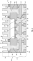
- Figure 2 is a schematic side sectional view showing an example of an integrated device package 40 including an integrated heat sink 33, according to an embodiment.
- the integrated device package 40 can also be used in any suitable type of electronic system.
- the integrated device package 40 can be utilized for a high power application (e.g. , a high power regulator).
- the integrated device package 40 can include an electronic component package 21 and the integrated heat sink 33.
- the electronic component package 21 can include a first insulating layer 22, a second insulating layer 23, a plurality of first vias 24, a plurality of second vias 30, a plurality of laterally-extending traces 31, a plurality of packaging terminations 25, a protective material 26, a second layer 27 of protective material, an electronic component 28 and a plurality of contact pads 29 (which electrically connect the electronic component 28 to the metallization 32), as well as a first surface 41 and a second surface 42.
- the metallization 32 can include the vias 24, 30 which provide vertical communication through the protective material 26 and the second insulating layer 23, respectively. Furthermore, the metallization 32 can also include the laterally-extending traces 31 that provide horizontal electrical communication within the integrated device package 40.
- the metallization 12 can comprise any suitable type of metal, such as, e.g. , copper, as would be known to one of ordinary skill in the art.
- the heat sink 33 can include a plurality of projections 34 and a plurality of insulating portions 35 between corresponding projections 34.
- the insulating portions 35 can comprise a gas (e.g ., air) in some embodiments, such that the gas is provided between the projections 34.
- a solid state insulating materials such as an organic or inorganic dielectric
- the electronic component 28 can comprise any suitable type of electronic component, such as an integrated device die (which can include active circuitry therein), a passive electronic device (such as a capacitor, an inductor, a resistor, a transformer, etc.), or any other suitable type of device.
- the electronic component 28 can connect to the metallization 32 by way of the contact pads 29.
- the electronic component 28 can be embedded within the protective material 26, and coupled to packaging terminations 25 through the contact pads 29 and the second vias 30.
- the electronic component 28 can be placed between the first insulating layer 22 and the second insulating layer 23, wherein the first insulating layer 22 and the second insulating layer 23 can be connected by the first vias 24.
- the second insulating layer 23 can be placed over a substrate such as a system board, e.g. , a PCB (not shown) and coupled to the PCB, for example, by way of solder bumps (not shown).
- the packaging terminations 25 can be, e.g. , a BGA or an LGA.
- the packaging terminations 25 can be disposed over the PCB and spaced apart along the second surface 42 in a pattern corresponding to, e.g. , the BGA or the LGA, and provide electrical connection between the electronic component 28 and the PCB.
- the electronic component 28 can comprise a die of one or more layers. In another embodiment, there can be more than one electronic component 28 embedded within the molding material 26.
- the foregoing structure of the electronic component package 21 can generate power of at least 100 W, at least 500 W, at least 1 kW, or at least 3 kW. In some embodiments, it can generate power in a range of 100 W to 5 kW, in a range of 500 W to 5 kW, in a range of 1 kW to 5 kW, or in a range of 3 kW to 5 kW. In some applications, it can operate at one or more frequencies in a range of 30 kHz to 3 MHz, in a range of 100 kHz to 3 MHz, or in a range of 1 MHz to 3 MHz.
- the inductance can be at least 10 ⁇ H, at least 50 ⁇ H, or at least 100 ⁇ H, for example, in a range of 10 ⁇ H to 100 ⁇ H.
- the heat sink 33 can be added to the first surface 41 of the electronic component package 21, to dissipate the generated heat. For example, based on the heat sink 33 directly contacting the first vias 24, most heat can be pulled away.
- the heat sink 33 can include the projections 34, which can be spaced apart by the insulating portions 35.
- the projections 34 can extend from a base portion that contacts the first surface 41, and away from the electronic component package 21.
- the first vias 24 can provide a thermal connection to the electronic component 28, and provide, e.g. , a thermal pathway for the generated heat discussed herein to be dissipated from the component 28 through the heat sink 33.
- the integrated device package 40 can achieve a more efficient heat dissipating characteristics than adding a heat sink with an adhesive.
- the heat sink 33 can comprise a metal layer that is added on the first surface 41 of the electronic component package 21.
- the heat sink 33 can be added by, e.g. , electroplating the heat sink 33 onto ( e.g. , directly onto) the first insulating layer 22 and the upper pads 36 of the metallization 32.
- the dry film patterning or photolithography can allow the metal layer to be patterned to mimic a shape of a heat sink.
- the metal layer can be plated with pins or fins. Electroplating the heat sink 33 onto the surface 41 of the electronic component package 21 can accordingly be performed without an adhesive between the electronic component package 21 and the heat sink 33.
- the electroplated metallic portion of the heat sink 33 can directly contact the portions of the insulating layer 22 and the portions of the metallization 32 over which the heat sink is deposited.
- the patterned metal layer i.e. , the heat sink 33
- the projections 34 can be spaced apart by the insulating portions 35, which can comprise a gas such as air or a solid-state insulating material, such that heat can be conveyed away from the integrated device package 40.
- Various embodiments utilizing the plating and photolithography processes developed as part of an embedded die manufacturing process can employ an inductor/ferrite manufacturing process to provide a thermally enhanced integrated device package 40 (e.g ., high power inductors and transformers). This can be achieved by manufacturing inductors using the different metal layers in the structure to create parallel inductor windings between the metal layers, and can be further improved by incorporating ferrous dielectric layers between the metal layers to increase the inductance. Because the plating and photolithography process are used to provide the heat sink 33, manufacturing of the integrated device package 40 provides a solution that does not add significantly to the material and process costs.
- an inductor/ferrite manufacturing process to provide a thermally enhanced integrated device package 40 (e.g ., high power inductors and transformers). This can be achieved by manufacturing inductors using the different metal layers in the structure to create parallel inductor windings between the metal layers, and can be further improved by incorporating ferrous dielectric layers between the metal layers to increase the inductance. Because the plating
- the integrated device package 40 with the integrated heat sink 33 can be integrated into a manufacturing process with little to no impact to pricing. Further, as explained above, increasing the available surface area of the heat sink by proper design of the heat sinks pins and fins for improved convective thermal dissipative properties can provide the ability to operate the finished module at high dissipative power densities.
- the heat sink 33 can be added onto ( e.g. , plated directly onto and contacting) the electronic component package 21 wherein the first surface 41 ( Figure 3 ) may be, in some embodiments, the first insulating layer 22 ( i.e. , the entire surface of the electronic component package 21 facing the heat sink 33) or, in other embodiments, the first insulating layer 22 and the exposed upper surface of the electronic component 28 ( Figure 4 ). This can be important when electrical isolation between the die and the heat sink is required.
- the shape of the heat sink 33 can be formed or modified so as to include the heat-dissipating projections 34 as, e.g ., a fin-type ( Figure 5 ) or pin-type ( Figure 6 ) heat sink.
- the projections 34 can comprise a plurality of elongated fins.
- the fins in Figure 5 can extend across a width of the first surface 41.
- the fins in Figure 5 can be spaced along a length of the first surface 41 in a one-dimensional (1D) array of projections 34.
- the projections 34 can comprise a plurality of pins disposed in an array over the first surface 41.
- the pins of Figure 6 can be disposed in a two-dimensional (2D) array in which pins are spaced apart along the width and length of the first surface 41.
- the integrated device package 40 may not include a separate heat sink structure that is adhered with an adhesive.
- the integrated device package 40 can include any suitable type of electronic component 28.
- the electronic component 28 can comprise a semiconductor die, such as a processor die, a memory die, a sensor die, a microelectromechanical systems die, etc.
- the packaging terminations 25 can connect to any suitable carrier. In the illustrated embodiment, the packaging terminations 25 can be disposed on the second surface 42 of the electronic component package 21.
- Figure 7 is a flow chart showing a method 50 of manufacturing an integrated device package 40 including an integrated heat sink 33, according to an embodiment.
- the method 50 comprises at least partially embedding an electronic component 28 within a protective material 26.
- the electronic component 28 can be only partially embedded within the protective material 26.
- the electronic component 28 may be exposed through the protective material 26 in some embodiments (see Figure 4 ).
- the electronic component 28 can be embedded completely within the protective material 26 (see Figure 3 ).
- the integrated device package 40 can have additional vias ( e.g ., through the protective material 26) to at least thermally connect the electronic component 28 to the heat sink 33.
- the method 50 comprises electroplating a heat sink 33 on a first surface of an electronic component package 21.
- electroplating the heat sink 33 can include utilizing the plating and photolithography processes developed as part of an embedded die manufacturing process to provide a thermally enhanced integrated device package 40 (e . g ., high power inductors and transformers).
- the integrated device package 40 with the embedded heat sink 33 can be economically integrated into a molded packaging process. Further, as explained above, increasing the available surface area for improved convective thermal dissipative properties can provide the ability to operate the finished module at high dissipative power densities.
- electroplating the heat sink 33 can comprise forming the projections 34 that are fin-type ( Figure 5 ) or pin-type ( Figure 6 ), it can also include forming the projections 34 in any other way so as to increase the available surface area of the heat sink 33 for heat dissipation.
- the words “comprise,” “comprising,” “include,” “including” and the like are to be construed in an inclusive sense, as opposed to an exclusive or exhaustive sense; that is to say, in the sense of "including, but not limited to.”
- the word “coupled”, as generally used herein, refers to two or more elements that may be either directly connected, or connected by way of one or more intermediate elements.
- the word “connected”, as generally used herein, refers to two or more elements that may be either directly connected, or connected by way of one or more intermediate elements.
- conditional language used herein such as, among others, “can,” “could,” “might,” “may,” “e.g.,” “for example,” “such as” and the like, unless specifically stated otherwise, or otherwise understood within the context as used, is generally intended to convey that certain embodiments include, while other embodiments do not include, certain features, elements and/or states. Thus, such conditional language is not generally intended to imply that features, elements and/or states are in any way required for one or more embodiments.
Landscapes
- Cooling Or The Like Of Semiconductors Or Solid State Devices (AREA)
Abstract
Description
- Any and all applications for which a foreign or domestic priority claim is identified in the Application Data Sheet as filed with the present application are hereby incorporated by reference under 37 CFR 1.57.
- The field relates to an electronic device and, in particular, to an integrated device package with an embedded heat sink.
- Various electronic devices (e.g., high power regulators), due to various inefficiencies, generate heat that should be dissipated. Otherwise, the generated heat may degrade or limit the product performance. Accordingly, there is a continuing need for improved electronic devices with efficient solutions for dissipating the generated heat.
- In one embodiment, an integrated device package can include an electronic component package. The electronic component package can comprise an electronic component; and a protective material in which the electronic component is at least partially embedded. The electronic component package can comprise a first surface and a second surface; and a heat sink plated onto the first surface.
- In some embodiments, the electronic component comprises a passive electronic device. In some embodiments, the electronic component comprises an integrated device die. In some embodiments, the electronic component is partially embedded within the protective material, the heat sink plated onto an exposed surface of the electronic component. In some embodiments, the electronic component comprises an insulating layer over the protective material, wherein the electronic component is completely embedded within the protective material, the heat sink plated onto the insulating layer. In some embodiments, the electronic component is completely embedded within the protective material. In some embodiments, the heat sink is connected to the electronic component by at least one via, the at least one via disposed within the protective material and connecting the heat sink and the electronic component at least thermally. In some embodiments, the heat sink comprises a shaped metal layer provided over the first surface of the electronic component package. In some embodiments, the heat sink comprises a base portion and a plurality of projections extending in a direction away from the electronic component, the projections comprising fins spaced apart along one dimension of the first surface. In some embodiments, the heat sink comprises a base portion and a plurality of projections extending in a direction away from the electronic component, the projections comprising pins spaced apart in a two-dimensional (2D) array along a width and a length of the first surface.
- In another embodiment, a method of manufacturing an integrated device package is disclosed. The method can include: at least partially embedding an electronic component within a protective material of an electronic component package, the electronic component package comprising a first surface and a second surface; and electroplating a heat sink onto the first surface.
- In some embodiments, the electronic component comprises a passive electronic device. In some embodiments, the electronic component comprises an integrated device die. In some embodiments, at least partially embedding the electronic component comprises partially embedding the electronic component within the protective material so as to expose at least a portion of the electronic component through the protective material. In some embodiments, electroplating the heat sink comprises adding a metal layer over the first surface and plating the metal layer such that the metal layer directly contacts the electronic component. In some embodiments, at least partially embedding the electronic component comprises completely embedding the electronic component within the protective material. In some embodiments, electroplating the heat sink comprises adding a metal layer over the first surface and plating the metal layer such that the metal layer contacts an insulating layer over the protective material. In some embodiments, electroplating the heat sink comprises adding a metal layer over the first surface and forming, by a photolithography process, the metal layer in a shape for dissipating heat. In some embodiments, forming the metal layer in the shape for dissipating the heat comprises forming a plurality of projections extending in a direction away from the electronic component, the projections comprising fins spaced apart along one dimension of the first surface, wherein the space between the fins comprises a plurality of insulating portions. In some embodiments, forming the metal layer in the shape for dissipating the heat comprises forming a plurality of projections extending in a direction away from the electronic component, the projections comprising pins spaced apart in a two-dimensional (2D) array along a width and a length of the first surface, wherein the space between the pins comprises a plurality of insulating portions.
- Embodiments of this disclosure will now be described, by way of non-limiting example, with reference to the accompanying drawings.
-
Figure 1 is a schematic side sectional view of an electronic component package. -
Figure 2 is a schematic side sectional view showing an example of an integrated device package including an integrated heat sink, according to an embodiment. -
Figure 3 is a schematic perspective view showing an example of an electronic component package before a heat sink is added. -
Figure 4 is a schematic perspective view showing another example of an electronic component package before a heat sink is added. -
Figure 5 is a schematic perspective view showing an example of an integrated device package with a heat sink including a plurality of elongate fins. -
Figure 6 is a schematic perspective view showing another example of an integrated device package with a heat sink including an array of vertically-extending pins. -
Figure 7 is a flow chart showing a method of manufacturing an integrated device package including an embedded heat sink, according to an embodiment. - Electronic devices, including integrated circuit dies, can comprise devices that generate a significant amount of power. Heat generated from the dies can be dissipated in a variety of ways. With respect to electronic devices that generate heat, there are several ways in which the heat can be dissipated. An example heat dissipation pathway includes a pathway down into the system board (i.e., by a thermally-conductive pathway to the board). In many cases, the system boards are very dense and have many heat-generating components, and it is not feasible or desirable to pull all of the heat through the system board. Thus, other structures (e.g., heat sinks, cold plates, fans, etc.) are utilized with the electronic devices to improve the heat dissipation through the top of the components.
- Some solutions typically add the other structures such as heat sinks as separate components. These increase cost (e.g., via added material and processes) and are not as efficient because of high thermally resistant polymers and adhesives used to attach, e.g., the heat sinks to the electronic devices.
- Thus, as described herein, the package manufacturing process (e.g., to embed a die or component into a molding material) can be used to add an integrated heat sink into an electronic component package, which would not incur the increased costs discussed above. For example, a final top metal layer can be added and patterned to provide increased surface area to improve the convection cooling and heat dissipation characteristics of the package. The top metal pattern can mimic a heat sink (e.g., a pin-type or fin-type heat sink), but can be manufactured using plating technologies rather than being adhered to the package.
-
Figure 1 is a schematic side sectional view of an electronic component package 1, according to some implementations. The electronic component package 1 can be used in any suitable type of electronic system, and can be packaged in any suitable manner. The electronic component package 1 can include a first insulating layer 2, a secondinsulating layer 3, a plurality of first vias 4, a plurality ofsecond vias 10, a plurality of laterally-extendingtraces 11, a plurality ofpackaging terminations 5, aprotective material 6, a second layer 7 of protective material, anelectronic component 8 and a plurality ofcontact pads 9 that electrically connect thecomponent 8 to themetallization 12. Themetallization 12 can comprise any suitable type of metal, such as, e.g., copper, as would be known to one of ordinary skill in the art. In various embodiments, the protective material can comprise an organic or polymer coating. For example, the protective material can comprise a molding compound in some embodiments. In other embodiments, the protective material can comprise a film, e.g., an organic epoxy resin which may include inorganic microparticle fillers, such as Ajinomoto Build-up Film (ABF), sold by Ajinomoto Group of Tokyo, Japan. - The
electronic component 8 can comprise any suitable type of electronic component, such as an integrated device die (which can include active circuitry therein), a passive electronic device (such as a capacitor, an inductor, a resistor, a transformer, etc.), or any other suitable type of device. Thecomponent 8 can connect to themetallization 12 by way of thecontact pads 9. - As shown, the
electronic component 8 can be embedded within theprotective material 6, and coupled to thepackaging terminations 5 through thecontact pads 9 and thesecond vias 10. Theelectronic component 8 can be placed between the first insulating layer 2 and the secondinsulating layer 3, wherein the first insulating layer 2 and the secondinsulating layer 3 can be connected by the first vias 4. The secondinsulating layer 3 can be placed over a substrate such as a system board, e.g., a PCB (printed circuit board) (not shown). Thepackaging terminations 5 can be, e.g., a BGA (Ball Grid Array) or an LGA (Land Grid Array), and provide electrical connection to the PCB. Themetallization 12 can include thevias 4, 10 which provide vertical communication through theprotective material 6 and the second insulatinglayer 3, respectively. Themetallization 12 can also include the laterally-extendingtraces 11 that provide horizontal electrical communication within the package 1. -
Figure 2 is a schematic side sectional view showing an example of anintegrated device package 40 including anintegrated heat sink 33, according to an embodiment. Theintegrated device package 40 can also be used in any suitable type of electronic system. For example, theintegrated device package 40 can be utilized for a high power application (e.g., a high power regulator). Theintegrated device package 40 can include anelectronic component package 21 and theintegrated heat sink 33. Theelectronic component package 21 can include a first insulatinglayer 22, a second insulatinglayer 23, a plurality offirst vias 24, a plurality ofsecond vias 30, a plurality of laterally-extendingtraces 31, a plurality ofpackaging terminations 25, aprotective material 26, asecond layer 27 of protective material, anelectronic component 28 and a plurality of contact pads 29 (which electrically connect theelectronic component 28 to the metallization 32), as well as afirst surface 41 and asecond surface 42. Themetallization 32 can include thevias protective material 26 and the second insulatinglayer 23, respectively. Furthermore, themetallization 32 can also include the laterally-extendingtraces 31 that provide horizontal electrical communication within theintegrated device package 40. In some embodiments, themetallization 12 can comprise any suitable type of metal, such as, e.g., copper, as would be known to one of ordinary skill in the art. Theheat sink 33 can include a plurality ofprojections 34 and a plurality of insulatingportions 35 between correspondingprojections 34. The insulatingportions 35 can comprise a gas (e.g., air) in some embodiments, such that the gas is provided between theprojections 34. In other embodiments, however, a solid state insulating materials (such as an organic or inorganic dielectric) can serve as the insulatingportions 35 betweenadjacent projections 34. - The
electronic component 28 can comprise any suitable type of electronic component, such as an integrated device die (which can include active circuitry therein), a passive electronic device (such as a capacitor, an inductor, a resistor, a transformer, etc.), or any other suitable type of device. Theelectronic component 28 can connect to themetallization 32 by way of thecontact pads 29. - As shown, the
electronic component 28 can be embedded within theprotective material 26, and coupled topackaging terminations 25 through thecontact pads 29 and thesecond vias 30. Theelectronic component 28 can be placed between the first insulatinglayer 22 and the second insulatinglayer 23, wherein the first insulatinglayer 22 and the second insulatinglayer 23 can be connected by thefirst vias 24. The second insulatinglayer 23 can be placed over a substrate such as a system board, e.g., a PCB (not shown) and coupled to the PCB, for example, by way of solder bumps (not shown). The packaging terminations 25 can be, e.g., a BGA or an LGA. The packaging terminations 25 can be disposed over the PCB and spaced apart along thesecond surface 42 in a pattern corresponding to, e.g., the BGA or the LGA, and provide electrical connection between theelectronic component 28 and the PCB. - While not shown, in one embodiment, the
electronic component 28 can comprise a die of one or more layers. In another embodiment, there can be more than oneelectronic component 28 embedded within themolding material 26. - In some high power applications, the foregoing structure of the
electronic component package 21 can generate power of at least 100 W, at least 500 W, at least 1 kW, or at least 3 kW. In some embodiments, it can generate power in a range of 100 W to 5 kW, in a range of 500 W to 5 kW, in a range of 1 kW to 5 kW, or in a range of 3 kW to 5 kW. In some applications, it can operate at one or more frequencies in a range of 30 kHz to 3 MHz, in a range of 100 kHz to 3 MHz, or in a range of 1 MHz to 3 MHz. It can also accommodate high relative currents, including current in a range of 50 A to 1000 A, in a range of 100 A to 1000 A, or in a range of 500 A to 1000 A. In some embodiments, it can comprise a passive device, such as an inductor or transformer. In embodiments that include an inductor, the inductance can be at least 10 µH, at least 50 µH, or at least 100 µH, for example, in a range of 10 µH to 100 µH. - Accordingly, high power devices like those disclosed herein can generate significant heat. Thus, it can be important to effectively remove the generated heat from, e.g., the
electronic component 28. As shown inFigure 2 , theheat sink 33 can be added to thefirst surface 41 of theelectronic component package 21, to dissipate the generated heat. For example, based on theheat sink 33 directly contacting thefirst vias 24, most heat can be pulled away. - In one embodiment, the
heat sink 33 can include theprojections 34, which can be spaced apart by the insulatingportions 35. Theprojections 34 can extend from a base portion that contacts thefirst surface 41, and away from theelectronic component package 21. Thefirst vias 24 can provide a thermal connection to theelectronic component 28, and provide, e.g., a thermal pathway for the generated heat discussed herein to be dissipated from thecomponent 28 through theheat sink 33. By providing a continuous connection between the vias 24, 30 and the heat sink 33 (i.e., without any added adhesive which may be highly thermally-resistant), theintegrated device package 40 can achieve a more efficient heat dissipating characteristics than adding a heat sink with an adhesive. - In one embodiment, the
heat sink 33 can comprise a metal layer that is added on thefirst surface 41 of theelectronic component package 21. For example, theheat sink 33 can be added by, e.g., electroplating theheat sink 33 onto (e.g., directly onto) the first insulatinglayer 22 and theupper pads 36 of themetallization 32. In one embodiment, the dry film patterning or photolithography can allow the metal layer to be patterned to mimic a shape of a heat sink. For example, the metal layer can be plated with pins or fins. Electroplating theheat sink 33 onto thesurface 41 of theelectronic component package 21 can accordingly be performed without an adhesive between theelectronic component package 21 and theheat sink 33. Accordingly, in the illustrated embodiment, the electroplated metallic portion of theheat sink 33 can directly contact the portions of the insulatinglayer 22 and the portions of themetallization 32 over which the heat sink is deposited. The patterned metal layer (i.e., the heat sink 33), with its increased surface area, can provide an improved heat dissipation for theintegrated device package 40 with convective cooling. As shown, for example, theprojections 34 can be spaced apart by the insulatingportions 35, which can comprise a gas such as air or a solid-state insulating material, such that heat can be conveyed away from theintegrated device package 40. - Various embodiments utilizing the plating and photolithography processes developed as part of an embedded die manufacturing process can employ an inductor/ferrite manufacturing process to provide a thermally enhanced integrated device package 40 (e.g., high power inductors and transformers). This can be achieved by manufacturing inductors using the different metal layers in the structure to create parallel inductor windings between the metal layers, and can be further improved by incorporating ferrous dielectric layers between the metal layers to increase the inductance. Because the plating and photolithography process are used to provide the
heat sink 33, manufacturing of theintegrated device package 40 provides a solution that does not add significantly to the material and process costs. By comparison, other solutions may experience increased material and processing costs, and may not be as efficient due to high thermally resistant polymers and adhesives used to attach separate components. In the embodiments disclosed herein, theintegrated device package 40 with theintegrated heat sink 33 can be integrated into a manufacturing process with little to no impact to pricing. Further, as explained above, increasing the available surface area of the heat sink by proper design of the heat sinks pins and fins for improved convective thermal dissipative properties can provide the ability to operate the finished module at high dissipative power densities. - In various embodiments, the
heat sink 33 can be added onto (e.g., plated directly onto and contacting) theelectronic component package 21 wherein the first surface 41 (Figure 3 ) may be, in some embodiments, the first insulating layer 22 (i.e., the entire surface of theelectronic component package 21 facing the heat sink 33) or, in other embodiments, the first insulatinglayer 22 and the exposed upper surface of the electronic component 28 (Figure 4 ). This can be important when electrical isolation between the die and the heat sink is required. - Moreover, in various embodiments, the shape of the
heat sink 33 can be formed or modified so as to include the heat-dissipatingprojections 34 as, e.g., a fin-type (Figure 5 ) or pin-type (Figure 6 ) heat sink. As illustrated herein inFigure 5 , for example, theprojections 34 can comprise a plurality of elongated fins. The fins inFigure 5 can extend across a width of thefirst surface 41. The fins inFigure 5 can be spaced along a length of thefirst surface 41 in a one-dimensional (1D) array ofprojections 34. In other embodiments, as shown inFigure 6 , theprojections 34 can comprise a plurality of pins disposed in an array over thefirst surface 41. The pins ofFigure 6 can be disposed in a two-dimensional (2D) array in which pins are spaced apart along the width and length of thefirst surface 41. Beneficially, theintegrated device package 40 may not include a separate heat sink structure that is adhered with an adhesive. - As explained herein, the
integrated device package 40 can include any suitable type ofelectronic component 28. For example, theelectronic component 28 can comprise a semiconductor die, such as a processor die, a memory die, a sensor die, a microelectromechanical systems die, etc. The packaging terminations 25 can connect to any suitable carrier. In the illustrated embodiment, thepackaging terminations 25 can be disposed on thesecond surface 42 of theelectronic component package 21. -
Figure 7 is a flow chart showing amethod 50 of manufacturing anintegrated device package 40 including anintegrated heat sink 33, according to an embodiment. - In
step 51, themethod 50 comprises at least partially embedding anelectronic component 28 within aprotective material 26. In one embodiment, theelectronic component 28 can be only partially embedded within theprotective material 26. For example, theelectronic component 28 may be exposed through theprotective material 26 in some embodiments (seeFigure 4 ). In another embodiment, theelectronic component 28 can be embedded completely within the protective material 26 (seeFigure 3 ). In some embodiments, theintegrated device package 40 can have additional vias (e.g., through the protective material 26) to at least thermally connect theelectronic component 28 to theheat sink 33. - In
step 52, themethod 50 comprises electroplating aheat sink 33 on a first surface of anelectronic component package 21. In one embodiment, as discussed herein, electroplating theheat sink 33 can include utilizing the plating and photolithography processes developed as part of an embedded die manufacturing process to provide a thermally enhanced integrated device package 40 (e.g., high power inductors and transformers). In the embodiments disclosed herein, theintegrated device package 40 with the embeddedheat sink 33 can be economically integrated into a molded packaging process. Further, as explained above, increasing the available surface area for improved convective thermal dissipative properties can provide the ability to operate the finished module at high dissipative power densities. Thus, while electroplating theheat sink 33 can comprise forming theprojections 34 that are fin-type (Figure 5 ) or pin-type (Figure 6 ), it can also include forming theprojections 34 in any other way so as to increase the available surface area of theheat sink 33 for heat dissipation. - Unless the context clearly requires otherwise, throughout the description and the claims, the words "comprise," "comprising," "include," "including" and the like are to be construed in an inclusive sense, as opposed to an exclusive or exhaustive sense; that is to say, in the sense of "including, but not limited to." The word "coupled", as generally used herein, refers to two or more elements that may be either directly connected, or connected by way of one or more intermediate elements. Likewise, the word "connected", as generally used herein, refers to two or more elements that may be either directly connected, or connected by way of one or more intermediate elements. Additionally, the words "herein," "above," "below," and words of similar import, when used in this application, shall refer to this application as a whole and not to any particular portions of this application. Moreover, as used herein, when a first element is described as being "on" or "over" a second element, the first element may be directly on or over the second element, such that the first and second elements directly contact, or the first element may be indirectly on or over the second element such that one or more elements intervene between the first and second elements. Where the context permits, words in the above Detailed Description using the singular or plural number may also include the plural or singular number respectively. Regarding the word "or" in reference to a list of two or more items, that word covers all of the following interpretations of the word: any of the items in the list, all of the items in the list, and any combination of the items in the list.
- Moreover, conditional language used herein, such as, among others, "can," "could," "might," "may," "e.g.," "for example," "such as" and the like, unless specifically stated otherwise, or otherwise understood within the context as used, is generally intended to convey that certain embodiments include, while other embodiments do not include, certain features, elements and/or states. Thus, such conditional language is not generally intended to imply that features, elements and/or states are in any way required for one or more embodiments.
- Although disclosed in the context of certain embodiments and examples, it will be understood by those skilled in the art that the present invention extends beyond the specifically disclosed embodiments to other alternative embodiments and/or uses and obvious modifications and equivalents thereof. Further, unless otherwise noted, the components of an illustration may be the same as or generally similar to like-numbered components of one or more different illustrations. In addition, while several variations have been shown and described in detail, other modifications, which are within the scope of this disclosure, will be readily apparent to those of skill in the art based upon this disclosure. It is also contemplated that various combinations or sub-combinations of the specific features and aspects of the embodiments may be made and still fall within the scope of the present disclosure. It should be understood that various features and aspects of the disclosed embodiments can be combined with, or substituted for, one another in order to form varying modes of the disclosed invention. Thus, it is intended that the scope of the present invention herein disclosed should not be limited by the particular disclosed embodiments described above, but should be determined only by a fair reading of the aspects that follow.
Claims (15)
- An integrated device package comprising:an electronic component package comprising:an electronic component; anda protective material in which the electronic component is at least partially embedded;wherein the electronic component package comprises a first surface and a second surface; anda heat sink plated onto the first surface.
- The integrated device package of Claim 1, wherein the electronic component comprises a passive electronic device.
- The integrated device package of Claim 1 or 2, wherein the electronic component comprises an integrated device die.
- The integrated device package of any preceding Claim, wherein the electronic component is partially embedded within the protective material, the heat sink plated onto an exposed surface of the electronic component.
- The integrated device package of any preceding Claim, wherein the electronic component is completely embedded within the protective material, and preferably the integrated device package further comprises an insulating layer over the protective material, and the heat sink plated onto the insulating layer.
- The integrated device package of any preceding Claim, wherein the heat sink is connected to the electronic component by at least one via, the at least one via disposed within the protective material and connecting the heat sink and the electronic component at least thermally.
- The integrated device package of any preceding Claim, wherein the heat sink comprises a shaped metal layer provided over the first surface of the electronic component package.
- The integrated device package of any preceding Claim, wherein the heat sink comprises a base portion and a plurality of projections extending in a direction away from the electronic component, the projections comprising fins spaced apart along one dimension of the first surface or the projections comprising pins spaced apart in a two-dimensional (2D) array along a width and a length of the first surface.
- A method of manufacturing an integrated device package, the method comprising:at least partially embedding an electronic component within a protective material of an electronic component package, the electronic component package comprising a first surface and a second surface; andelectroplating a heat sink onto the first surface.
- The method of Claim 9, wherein the electronic component comprises a passive electronic device.
- The method of Claim 9 or 10, wherein the electronic component comprises an integrated device die.
- The method of any of Claims 9 to 11, wherein at least partially embedding the electronic component comprises partially embedding the electronic component within the protective material so as to expose at least a portion of the electronic component through the protective material, and preferably wherein electroplating the heat sink comprises adding a metal layer over the first surface and plating the metal layer such that the metal layer directly contacts the electronic component.
- The method of any of Claims 9 to 12, wherein at least partially embedding the electronic component comprises completely embedding the electronic component within the protective material, and preferably wherein electroplating the heat sink comprises adding a metal layer over the first surface and plating the metal layer such that the metal layer contacts an insulating layer over the protective material.
- The method of any of Claims 9 to 13, wherein electroplating the heat sink comprises adding a metal layer over the first surface and forming, by a photolithography process, the metal layer in a shape for dissipating heat.
- The method of any of Claims 9 to 14, wherein forming the metal layer in the shape for dissipating the heat comprises forming a plurality of projections extending in a direction away from the electronic component, the projections comprising fins spaced apart along one dimension of the first surface or the projections comprising pins spaced apart in a two-dimensional (2D) array along a width and a length of the first surface, wherein the space between the fins comprises a plurality of insulating portions.
Applications Claiming Priority (1)
| Application Number | Priority Date | Filing Date | Title |
|---|---|---|---|
| US17/454,009 US12315776B2 (en) | 2021-11-08 | 2021-11-08 | Integrated device package with an integrated heat sink |
Publications (2)
| Publication Number | Publication Date |
|---|---|
| EP4177946A1 true EP4177946A1 (en) | 2023-05-10 |
| EP4177946B1 EP4177946B1 (en) | 2025-01-01 |
Family
ID=84361399
Family Applications (1)
| Application Number | Title | Priority Date | Filing Date |
|---|---|---|---|
| EP22205245.8A Active EP4177946B1 (en) | 2021-11-08 | 2022-11-03 | Integrated device package with an integrated heat sink |
Country Status (2)
| Country | Link |
|---|---|
| US (1) | US12315776B2 (en) |
| EP (1) | EP4177946B1 (en) |
Cited By (1)
| Publication number | Priority date | Publication date | Assignee | Title |
|---|---|---|---|---|
| US12315776B2 (en) | 2021-11-08 | 2025-05-27 | Analog Devices, Inc. | Integrated device package with an integrated heat sink |
Citations (4)
| Publication number | Priority date | Publication date | Assignee | Title |
|---|---|---|---|---|
| US8759147B2 (en) * | 2010-12-31 | 2014-06-24 | Samsung Electronics Co., Ltd. | Semiconductor packages and methods of fabricating the same |
| US9214404B1 (en) * | 2011-11-29 | 2015-12-15 | Hrl Laboratories, Llc | Apparatus for mounting microelectronic chips |
| US9484313B2 (en) * | 2013-02-27 | 2016-11-01 | Advanced Semiconductor Engineering, Inc. | Semiconductor packages with thermal-enhanced conformal shielding and related methods |
| US20190181116A1 (en) * | 2017-12-11 | 2019-06-13 | Semiconductor Components Industries, Llc | Fan-out structure for semiconductor packages and related methods |
Family Cites Families (133)
| Publication number | Priority date | Publication date | Assignee | Title |
|---|---|---|---|---|
| US4303934A (en) | 1979-08-30 | 1981-12-01 | Burr-Brown Research Corp. | Molded lead frame dual in line package including a hybrid circuit |
| JP3009788B2 (en) | 1991-11-15 | 2000-02-14 | 日本特殊陶業株式会社 | Package for integrated circuit |
| EP0562211A1 (en) | 1992-03-25 | 1993-09-29 | International Business Machines Corporation | Self-aligning fiber couplers |
| JP3159071B2 (en) | 1996-08-01 | 2001-04-23 | 株式会社日立製作所 | Electric device having radiating fins |
| US5689091A (en) | 1996-09-19 | 1997-11-18 | Vlsi Technology, Inc. | Multi-layer substrate structure |
| JP3354424B2 (en) | 1997-02-27 | 2002-12-09 | 三洋電機株式会社 | Semiconductor device and method of manufacturing semiconductor device |
| JPH11195550A (en) | 1998-01-06 | 1999-07-21 | Kureha Chem Ind Co Ltd | Coil part |
| US6075700A (en) | 1999-02-02 | 2000-06-13 | Compaq Computer Corporation | Method and system for controlling radio frequency radiation in microelectronic packages using heat dissipation structures |
| US6271060B1 (en) | 1999-09-13 | 2001-08-07 | Vishay Intertechnology, Inc. | Process of fabricating a chip scale surface mount package for semiconductor device |
| US6388336B1 (en) | 1999-09-15 | 2002-05-14 | Texas Instruments Incorporated | Multichip semiconductor assembly |
| US6326611B1 (en) | 1999-09-28 | 2001-12-04 | Raytheon Company | Integrated multiple sensor package |
| US6228682B1 (en) | 1999-12-21 | 2001-05-08 | International Business Machines Corporation | Multi-cavity substrate structure for discrete devices |
| KR100736000B1 (en) | 2000-03-29 | 2007-07-06 | 로무 가부시키가이샤 | Semiconductor device |
| US6459581B1 (en) | 2000-12-19 | 2002-10-01 | Harris Corporation | Electronic device using evaporative micro-cooling and associated methods |
| US20020090749A1 (en) | 2001-01-09 | 2002-07-11 | 3M Innovative Properties Company | Hermetic package for mems devices with integrated carrier |
| US6545345B1 (en) | 2001-03-20 | 2003-04-08 | Amkor Technology, Inc. | Mounting for a package containing a chip |
| US6787916B2 (en) | 2001-09-13 | 2004-09-07 | Tru-Si Technologies, Inc. | Structures having a substrate with a cavity and having an integrated circuit bonded to a contact pad located in the cavity |
| KR100442830B1 (en) | 2001-12-04 | 2004-08-02 | 삼성전자주식회사 | Low temperature hermetic sealing method having a passivation layer |
| US6490161B1 (en) | 2002-01-08 | 2002-12-03 | International Business Machines Corporation | Peripheral land grid array package with improved thermal performance |
| US6825108B2 (en) | 2002-02-01 | 2004-11-30 | Broadcom Corporation | Ball grid array package fabrication with IC die support structures |
| US6891239B2 (en) | 2002-03-06 | 2005-05-10 | The Charles Stark Draper Laboratory, Inc. | Integrated sensor and electronics package |
| US6657311B1 (en) | 2002-05-16 | 2003-12-02 | Texas Instruments Incorporated | Heat dissipating flip-chip ball grid array |
| JP2004063664A (en) | 2002-07-26 | 2004-02-26 | Murata Mfg Co Ltd | Multilayer ceramic substrate with cavity |
| US6821817B1 (en) | 2002-09-03 | 2004-11-23 | Asat Ltd. | Premolded cavity IC package |
| US6723585B1 (en) | 2002-10-31 | 2004-04-20 | National Semiconductor Corporation | Leadless package |
| JP4140632B2 (en) | 2002-12-13 | 2008-08-27 | 松下電器産業株式会社 | Multiple choke coil and electronic device using the same |
| JP2004200316A (en) | 2002-12-17 | 2004-07-15 | Shinko Electric Ind Co Ltd | Semiconductor device |
| TWI225299B (en) | 2003-05-02 | 2004-12-11 | Advanced Semiconductor Eng | Stacked flip chip package |
| JP4869546B2 (en) | 2003-05-23 | 2012-02-08 | ルネサスエレクトロニクス株式会社 | Semiconductor device |
| WO2004107439A1 (en) | 2003-05-28 | 2004-12-09 | Infineon Technologies Ag | An integrated circuit package employing a head-spreader member |
| US20050046003A1 (en) | 2003-08-26 | 2005-03-03 | Chung-Che Tsai | Stacked-chip semiconductor package and fabrication method thereof |
| DE10352002A1 (en) | 2003-11-07 | 2005-06-09 | Robert Bosch Gmbh | sensor module |
| JP2005175423A (en) | 2003-11-18 | 2005-06-30 | Denso Corp | Semiconductor package |
| US7411281B2 (en) | 2004-06-21 | 2008-08-12 | Broadcom Corporation | Integrated circuit device package having both wire bond and flip-chip interconnections and method of making the same |
| US7745927B2 (en) | 2004-06-29 | 2010-06-29 | Agere Systems Inc. | Heat sink formed of multiple metal layers on backside of integrated circuit die |
| US7045888B2 (en) | 2004-06-29 | 2006-05-16 | Macronix International Co., Ltd. | Ultra thin dual chip image sensor package structure and method for fabrication |
| JP4528058B2 (en) | 2004-08-20 | 2010-08-18 | アルプス電気株式会社 | Coiled powder magnetic core |
| US7196411B2 (en) | 2004-09-17 | 2007-03-27 | Taiwan Semiconductor Manufacturing Company, Ltd. | Heat dissipation for chip-on-chip IC packages |
| US20060097385A1 (en) * | 2004-10-25 | 2006-05-11 | Negley Gerald H | Solid metal block semiconductor light emitting device mounting substrates and packages including cavities and heat sinks, and methods of packaging same |
| US8164182B2 (en) | 2004-11-15 | 2012-04-24 | Stats Chippac Ltd. | Hyper thermally enhanced semiconductor package system comprising heat slugs on opposite surfaces of a semiconductor chip |
| US7098070B2 (en) | 2004-11-16 | 2006-08-29 | International Business Machines Corporation | Device and method for fabricating double-sided SOI wafer scale package with through via connections |
| US7217994B2 (en) | 2004-12-01 | 2007-05-15 | Kyocera Wireless Corp. | Stack package for high density integrated circuits |
| US20060138643A1 (en) | 2004-12-28 | 2006-06-29 | Daoqiang Lu | One step capillary underfill integration for semiconductor packages |
| US7249752B1 (en) | 2005-02-11 | 2007-07-31 | Foley Michael J | Hand tool for extracting a fastener from a material |
| US7408244B2 (en) | 2005-03-16 | 2008-08-05 | Advanced Semiconductor Engineering, Inc. | Semiconductor package and stack arrangement thereof |
| US7355289B2 (en) | 2005-07-29 | 2008-04-08 | Freescale Semiconductor, Inc. | Packaged integrated circuit with enhanced thermal dissipation |
| US7419853B2 (en) | 2005-08-11 | 2008-09-02 | Hymite A/S | Method of fabrication for chip scale package for a micro component |
| KR100659510B1 (en) | 2006-02-16 | 2006-12-20 | 삼성전기주식회사 | Cavity formed substrate manufacturing method |
| US7592202B2 (en) | 2006-03-31 | 2009-09-22 | Intel Corporation | Embedding device in substrate cavity |
| JP4222490B2 (en) | 2006-09-29 | 2009-02-12 | Tdk株式会社 | Planar transformer and switching power supply |
| TWI353047B (en) | 2006-12-28 | 2011-11-21 | Siliconware Precision Industries Co Ltd | Heat-dissipating-type semiconductor package |
| SI2149902T1 (en) | 2007-05-18 | 2019-03-29 | Sansha Electric Manufacturing Company, Limited | Power semiconductor module and arc discharge device using the same |
| US20080290502A1 (en) | 2007-05-25 | 2008-11-27 | Zafer Kutlu | Integrated circuit package with soldered lid for improved thermal performance |
| US7911059B2 (en) | 2007-06-08 | 2011-03-22 | SeniLEDS Optoelectronics Co., Ltd | High thermal conductivity substrate for a semiconductor device |
| US20090032926A1 (en) | 2007-07-31 | 2009-02-05 | Advanced Micro Devices, Inc. | Integrated Support Structure for Stacked Semiconductors With Overhang |
| US8136071B2 (en) | 2007-09-12 | 2012-03-13 | Neal Solomon | Three dimensional integrated circuits and methods of fabrication |
| US7920039B2 (en) | 2007-09-25 | 2011-04-05 | Flextronics Ap, Llc | Thermally enhanced magnetic transformer |
| US7619303B2 (en) | 2007-12-20 | 2009-11-17 | National Semiconductor Corporation | Integrated circuit package |
| US7998791B2 (en) | 2008-02-01 | 2011-08-16 | National Semiconductor Corporation | Panel level methods and systems for packaging integrated circuits with integrated heat sinks |
| US20090282917A1 (en) | 2008-05-19 | 2009-11-19 | Cenk Acar | Integrated multi-axis micromachined inertial sensing unit and method of fabrication |
| TW201004857A (en) | 2008-07-23 | 2010-02-01 | Ind Tech Res Inst | A packaging structure and method for integration of microelectronics and MEMS devices by 3D stacking |
| US8080925B2 (en) | 2008-09-23 | 2011-12-20 | Custom Sensors & Technologies, Inc. | Inertial sensor with dual cavity package and method of fabrication |
| US8115286B2 (en) | 2008-10-22 | 2012-02-14 | Honeywell International Inc. | Integrated sensor including sensing and processing die mounted on opposite sides of package substrate |
| JP5147677B2 (en) * | 2008-12-24 | 2013-02-20 | 新光電気工業株式会社 | Manufacturing method of resin-sealed package |
| US8405115B2 (en) | 2009-01-28 | 2013-03-26 | Maxim Integrated Products, Inc. | Light sensor using wafer-level packaging |
| JP5280880B2 (en) | 2009-02-10 | 2013-09-04 | 株式会社日立製作所 | Semiconductor integrated circuit device |
| US8405197B2 (en) | 2009-03-25 | 2013-03-26 | Stats Chippac Ltd. | Integrated circuit packaging system with stacked configuration and method of manufacture thereof |
| US20110024899A1 (en) | 2009-07-28 | 2011-02-03 | Kenji Masumoto | Substrate structure for cavity package |
| US8232142B2 (en) | 2009-09-14 | 2012-07-31 | Tyco Electronics Services Gmbh | Self-aligned silicon carrier for optical device supporting wafer scale methods |
| JP2011100932A (en) * | 2009-11-09 | 2011-05-19 | Toshiba Corp | Semiconductor package and dc-dc converter |
| US9202769B2 (en) | 2009-11-25 | 2015-12-01 | Stats Chippac, Ltd. | Semiconductor device and method of forming thermal lid for balancing warpage and thermal management |
| JP2011139024A (en) | 2009-12-04 | 2011-07-14 | Seiko Epson Corp | Package and vibrating device using the same |
| US20110163428A1 (en) | 2010-01-05 | 2011-07-07 | Manolito Fabres Galera | Semiconductor packages with embedded heat sink |
| US9385095B2 (en) | 2010-02-26 | 2016-07-05 | Taiwan Semiconductor Manufacturing Company, Ltd. | 3D semiconductor package interposer with die cavity |
| CN102256443B (en) | 2010-04-02 | 2015-12-16 | 雅达电子国际有限公司 | Sensor occupying space above circuit board components |
| US9215519B2 (en) | 2010-07-30 | 2015-12-15 | Invensense, Inc. | Reduced footprint microphone system with spacer member having through-hole |
| US8284561B2 (en) | 2010-08-05 | 2012-10-09 | Advanced Semiconductor Engineering, Inc. | Embedded component package structure |
| US9156673B2 (en) | 2010-09-18 | 2015-10-13 | Fairchild Semiconductor Corporation | Packaging to reduce stress on microelectromechanical systems |
| US20120098117A1 (en) | 2010-10-22 | 2012-04-26 | Renesas Technology America, Inc. | Power and thermal design using a common heat sink on top of high thermal conductive resin package |
| US8865525B2 (en) | 2010-11-22 | 2014-10-21 | Bridge Semiconductor Corporation | Method of making cavity substrate with built-in stiffener and cavity substrate manufactured thereby |
| JP5523299B2 (en) | 2010-12-20 | 2014-06-18 | 株式会社日立製作所 | Power module |
| US8772817B2 (en) | 2010-12-22 | 2014-07-08 | Cree, Inc. | Electronic device submounts including substrates with thermally conductive vias |
| US8409917B2 (en) | 2011-03-22 | 2013-04-02 | Stats Chippac Ltd. | Integrated circuit packaging system with an interposer substrate and method of manufacture thereof |
| KR101801945B1 (en) | 2011-08-09 | 2017-11-28 | 에스케이하이닉스 주식회사 | Semiconductor chip and semiconductor package having the same |
| US8653635B2 (en) | 2011-08-16 | 2014-02-18 | General Electric Company | Power overlay structure with leadframe connections |
| EP2568063A1 (en) * | 2011-09-09 | 2013-03-13 | Rohm and Haas Electronic Materials LLC | Low internal stress copper electroplating method |
| US20130069218A1 (en) | 2011-09-20 | 2013-03-21 | Stmicroelectronics Asia Pacific Pte Ltd. | High density package interconnect with copper heat spreader and method of making the same |
| CN103814627A (en) | 2011-09-21 | 2014-05-21 | 莫塞德技术公司 | Method and apparatus for connecting inlaid chip into printed circuit board |
| JP6014907B2 (en) | 2011-12-22 | 2016-10-26 | インテル・コーポレーション | 3D integrated circuit package with window interposer |
| US8842951B2 (en) | 2012-03-02 | 2014-09-23 | Analog Devices, Inc. | Systems and methods for passive alignment of opto-electronic components |
| US8920616B2 (en) * | 2012-06-18 | 2014-12-30 | Headway Technologies, Inc. | Paddle for electroplating for selectively depositing greater thickness |
| US8946879B2 (en) | 2012-07-27 | 2015-02-03 | Analog Devices, Inc. | Packages and methods for 3D integration including two stacked dies with a portion of one die extending into a hole of the other die |
| JP5945326B2 (en) | 2012-07-30 | 2016-07-05 | パナソニック株式会社 | Semiconductor device with heat dissipation structure |
| DE102012109028A1 (en) * | 2012-09-25 | 2014-03-27 | Osram Opto Semiconductors Gmbh | Optoelectronic semiconductor component and method for producing an optoelectronic semiconductor component |
| US9508674B2 (en) | 2012-11-14 | 2016-11-29 | Taiwan Semiconductor Manufacturing Company, Ltd. | Warpage control of semiconductor die package |
| JP5738326B2 (en) | 2013-01-14 | 2015-06-24 | 株式会社日本自動車部品総合研究所 | Power supply |
| US10566482B2 (en) | 2013-01-31 | 2020-02-18 | Global Graphene Group, Inc. | Inorganic coating-protected unitary graphene material for concentrated photovoltaic applications |
| US9209121B2 (en) | 2013-02-01 | 2015-12-08 | Analog Devices, Inc. | Double-sided package |
| EP2769956B1 (en) | 2013-02-20 | 2016-08-24 | Harman Becker Automotive Systems GmbH | Circuit board comprising spatial light modulator |
| JP5851439B2 (en) | 2013-03-07 | 2016-02-03 | 株式会社東芝 | High frequency semiconductor package |
| US9102513B1 (en) | 2014-01-29 | 2015-08-11 | Himax Display, Inc. | MEMS package structure |
| US9768090B2 (en) | 2014-02-14 | 2017-09-19 | Taiwan Semiconductor Manufacturing Company, Ltd. | Substrate design for semiconductor packages and method of forming same |
| SG10201400390YA (en) * | 2014-03-05 | 2015-10-29 | Delta Electronics Int L Singapore Pte Ltd | Package structure |
| US10121768B2 (en) | 2015-05-27 | 2018-11-06 | Bridge Semiconductor Corporation | Thermally enhanced face-to-face semiconductor assembly with built-in heat spreader and method of making the same |
| SG10201401622RA (en) * | 2014-04-17 | 2015-11-27 | Delta Electronics Int’L Singapore Pte Ltd | Package structure |
| FR3023059B1 (en) | 2014-06-25 | 2018-01-05 | Commissariat A L'energie Atomique Et Aux Energies Alternatives | INTEGRATED CIRCUIT COMPRISING A HEAT SINK |
| US9403674B2 (en) | 2014-08-12 | 2016-08-02 | Taiwan Semiconductor Manufacturing Co., Ltd. | Methods for packaging a microelectromechanical system (MEMS) wafer and application-specific integrated circuit (ASIC) dies using through mold vias (TMVs) |
| US9735130B2 (en) | 2014-08-29 | 2017-08-15 | Taiwan Semiconductor Manufacturing Company, Ltd. | Chip packages and methods of manufacture thereof |
| US9731959B2 (en) | 2014-09-25 | 2017-08-15 | Analog Devices, Inc. | Integrated device packages having a MEMS die sealed in a cavity by a processor die and method of manufacturing the same |
| US9735084B2 (en) | 2014-12-11 | 2017-08-15 | Invensas Corporation | Bond via array for thermal conductivity |
| US9533878B2 (en) | 2014-12-11 | 2017-01-03 | Analog Devices, Inc. | Low stress compact device packages |
| JP2017050358A (en) | 2015-08-31 | 2017-03-09 | トヨタ自動車株式会社 | Semiconductor device |
| US9659844B2 (en) | 2015-08-31 | 2017-05-23 | Texas Instruments Incorporated | Semiconductor die substrate with integral heat sink |
| US9761571B2 (en) | 2015-09-17 | 2017-09-12 | Deca Technologies Inc. | Thermally enhanced fully molded fan-out module |
| JP6402942B2 (en) | 2015-12-11 | 2018-10-10 | 株式会社オートネットワーク技術研究所 | Electrical junction box |
| US9913361B2 (en) * | 2016-01-06 | 2018-03-06 | International Business Machines Corporation | Integrated circuit device assembly |
| US11222973B2 (en) * | 2016-04-11 | 2022-01-11 | Mitsubishi Electric Corporation | Semiconductor device |
| JP6669586B2 (en) | 2016-05-26 | 2020-03-18 | 新光電気工業株式会社 | Semiconductor device and method of manufacturing semiconductor device |
| US10121766B2 (en) | 2016-06-30 | 2018-11-06 | Micron Technology, Inc. | Package-on-package semiconductor device assemblies including one or more windows and related methods and packages |
| JP6737009B2 (en) | 2016-06-30 | 2020-08-05 | 株式会社デンソー | Semiconductor device and manufacturing method thereof |
| US10395819B2 (en) | 2016-08-30 | 2019-08-27 | Astec International Limited | Multiple phase power converters having integrated magnetic cores for transformer and inductor windings |
| KR102527409B1 (en) * | 2016-12-19 | 2023-05-02 | 에스케이하이닉스 주식회사 | Semiconductor package including heat transferring block between chips and methods for manufacturing the same |
| JP6766734B2 (en) | 2017-04-03 | 2020-10-14 | トヨタ自動車株式会社 | How to make a heat sink |
| JP6958164B2 (en) | 2017-05-23 | 2021-11-02 | 株式会社オートネットワーク技術研究所 | Coil device, coil device with substrate and electrical junction box |
| JP6614210B2 (en) | 2017-07-27 | 2019-12-04 | Tdk株式会社 | Power receiving apparatus and wireless power transmission system |
| US10529677B2 (en) | 2018-04-27 | 2020-01-07 | Advanced Micro Devices, Inc. | Method and apparatus for power delivery to a die stack via a heat spreader |
| US20190393127A1 (en) | 2018-06-20 | 2019-12-26 | Semiconductor Components Industries, Llc | Semiconductor package with integrated heat sink |
| US10651109B2 (en) | 2018-07-16 | 2020-05-12 | Infineon Technologies Ag | Selective plating of semiconductor package leads |
| CN109390127B (en) | 2018-11-12 | 2024-01-30 | 矽力杰半导体技术(杭州)有限公司 | Supportable package device and package assembly |
| US11127524B2 (en) | 2018-12-14 | 2021-09-21 | Hong Kong Applied Science and Technology Research Institute Company Limited | Power converter |
| US11296005B2 (en) | 2019-09-24 | 2022-04-05 | Analog Devices, Inc. | Integrated device package including thermally conductive element and method of manufacturing same |
| US20210134510A1 (en) | 2019-10-31 | 2021-05-06 | Analog Devices International Unlimited Company | Electronic device |
| US12315776B2 (en) | 2021-11-08 | 2025-05-27 | Analog Devices, Inc. | Integrated device package with an integrated heat sink |
-
2021
- 2021-11-08 US US17/454,009 patent/US12315776B2/en active Active
-
2022
- 2022-11-03 EP EP22205245.8A patent/EP4177946B1/en active Active
Patent Citations (4)
| Publication number | Priority date | Publication date | Assignee | Title |
|---|---|---|---|---|
| US8759147B2 (en) * | 2010-12-31 | 2014-06-24 | Samsung Electronics Co., Ltd. | Semiconductor packages and methods of fabricating the same |
| US9214404B1 (en) * | 2011-11-29 | 2015-12-15 | Hrl Laboratories, Llc | Apparatus for mounting microelectronic chips |
| US9484313B2 (en) * | 2013-02-27 | 2016-11-01 | Advanced Semiconductor Engineering, Inc. | Semiconductor packages with thermal-enhanced conformal shielding and related methods |
| US20190181116A1 (en) * | 2017-12-11 | 2019-06-13 | Semiconductor Components Industries, Llc | Fan-out structure for semiconductor packages and related methods |
Cited By (1)
| Publication number | Priority date | Publication date | Assignee | Title |
|---|---|---|---|---|
| US12315776B2 (en) | 2021-11-08 | 2025-05-27 | Analog Devices, Inc. | Integrated device package with an integrated heat sink |
Also Published As
| Publication number | Publication date |
|---|---|
| US12315776B2 (en) | 2025-05-27 |
| US20230142729A1 (en) | 2023-05-11 |
| EP4177946B1 (en) | 2025-01-01 |
Similar Documents
| Publication | Publication Date | Title |
|---|---|---|
| US7511365B2 (en) | Thermal enhanced low profile package structure | |
| US9425131B2 (en) | Package structure | |
| US6212076B1 (en) | Enhanced heat-dissipating printed circuit board package | |
| US6549409B1 (en) | Power converter assembly | |
| JP5992368B2 (en) | Package carrier | |
| US7405102B2 (en) | Methods and apparatus for thermal management in a multi-layer embedded chip structure | |
| US12300424B2 (en) | Stacked electronic structure | |
| US20070090517A1 (en) | Stacked die package with thermally conductive block embedded in substrate | |
| KR20090034889A (en) | Chip module for complete power train | |
| WO2001006821A1 (en) | Encapsulated packaging in between 2 pcbs | |
| KR20160007455A (en) | Printed circuit board | |
| KR20120051992A (en) | Radiant heat substrate and method for manufacturing the radiant heat substrate, and package structure with the radiant heat substrate | |
| JP4987231B2 (en) | Thermally conductive substrate package | |
| US7309838B2 (en) | Multi-layered circuit board assembly with improved thermal dissipation | |
| US12315776B2 (en) | Integrated device package with an integrated heat sink | |
| US7714451B2 (en) | Semiconductor package system with thermal die bonding | |
| US20210134510A1 (en) | Electronic device | |
| US7327028B2 (en) | Embedded heat spreader for folded stacked chip-scale package | |
| US11848146B2 (en) | Stacked electronic module and method to make the same | |
| US11862688B2 (en) | Integrated GaN power module | |
| KR20160105266A (en) | Intergrated heat sink power module packege | |
| KR101140429B1 (en) | Radiant heat circuit board and manufacturing method thereof | |
| CN107527824B (en) | Package carrier with heat sink and method of making the same | |
| US20260026400A1 (en) | High density device package and packaging technique thereof | |
| KR101142036B1 (en) | Multi layer printed circuit board and method for manufacturing the same |
Legal Events
| Date | Code | Title | Description |
|---|---|---|---|
| PUAI | Public reference made under article 153(3) epc to a published international application that has entered the european phase |
Free format text: ORIGINAL CODE: 0009012 |
|
| STAA | Information on the status of an ep patent application or granted ep patent |
Free format text: STATUS: REQUEST FOR EXAMINATION WAS MADE |
|
| 17P | Request for examination filed |
Effective date: 20221103 |
|
| AK | Designated contracting states |
Kind code of ref document: A1 Designated state(s): AL AT BE BG CH CY CZ DE DK EE ES FI FR GB GR HR HU IE IS IT LI LT LU LV MC ME MK MT NL NO PL PT RO RS SE SI SK SM TR |
|
| STAA | Information on the status of an ep patent application or granted ep patent |
Free format text: STATUS: EXAMINATION IS IN PROGRESS |
|
| 17Q | First examination report despatched |
Effective date: 20240115 |
|
| GRAP | Despatch of communication of intention to grant a patent |
Free format text: ORIGINAL CODE: EPIDOSNIGR1 |
|
| STAA | Information on the status of an ep patent application or granted ep patent |
Free format text: STATUS: GRANT OF PATENT IS INTENDED |
|
| RIC1 | Information provided on ipc code assigned before grant |
Ipc: H01L 23/373 20060101ALN20240711BHEP Ipc: H01L 21/48 20060101ALI20240711BHEP Ipc: H01L 23/367 20060101ALI20240711BHEP Ipc: H01L 23/538 20060101AFI20240711BHEP |
|
| INTG | Intention to grant announced |
Effective date: 20240729 |
|
| RIC1 | Information provided on ipc code assigned before grant |
Ipc: H01L 23/373 20060101ALN20240719BHEP Ipc: H01L 21/48 20060101ALI20240719BHEP Ipc: H01L 23/367 20060101ALI20240719BHEP Ipc: H01L 23/538 20060101AFI20240719BHEP |
|
| RIN1 | Information on inventor provided before grant (corrected) |
Inventor name: OLSEN, EDWARD Inventor name: ANDERSON, MICHAEL JOHN |
|
| GRAS | Grant fee paid |
Free format text: ORIGINAL CODE: EPIDOSNIGR3 |
|
| GRAA | (expected) grant |
Free format text: ORIGINAL CODE: 0009210 |
|
| STAA | Information on the status of an ep patent application or granted ep patent |
Free format text: STATUS: THE PATENT HAS BEEN GRANTED |
|
| AK | Designated contracting states |
Kind code of ref document: B1 Designated state(s): AL AT BE BG CH CY CZ DE DK EE ES FI FR GB GR HR HU IE IS IT LI LT LU LV MC ME MK MT NL NO PL PT RO RS SE SI SK SM TR |
|
| REG | Reference to a national code |
Ref country code: GB Ref legal event code: FG4D |
|
| REG | Reference to a national code |
Ref country code: DE Ref legal event code: R096 Ref document number: 602022009294 Country of ref document: DE |
|
| REG | Reference to a national code |
Ref country code: CH Ref legal event code: EP |
|
| REG | Reference to a national code |
Ref country code: IE Ref legal event code: FG4D |
|
| REG | Reference to a national code |
Ref country code: LT Ref legal event code: MG9D |
|
| REG | Reference to a national code |
Ref country code: NL Ref legal event code: MP Effective date: 20250101 |
|
| REG | Reference to a national code |
Ref country code: AT Ref legal event code: MK05 Ref document number: 1757212 Country of ref document: AT Kind code of ref document: T Effective date: 20250101 |
|
| PG25 | Lapsed in a contracting state [announced via postgrant information from national office to epo] |
Ref country code: NL Free format text: LAPSE BECAUSE OF FAILURE TO SUBMIT A TRANSLATION OF THE DESCRIPTION OR TO PAY THE FEE WITHIN THE PRESCRIBED TIME-LIMIT Effective date: 20250101 |
|
| PG25 | Lapsed in a contracting state [announced via postgrant information from national office to epo] |
Ref country code: FI Free format text: LAPSE BECAUSE OF FAILURE TO SUBMIT A TRANSLATION OF THE DESCRIPTION OR TO PAY THE FEE WITHIN THE PRESCRIBED TIME-LIMIT Effective date: 20250101 |
|
| PG25 | Lapsed in a contracting state [announced via postgrant information from national office to epo] |
Ref country code: PL Free format text: LAPSE BECAUSE OF FAILURE TO SUBMIT A TRANSLATION OF THE DESCRIPTION OR TO PAY THE FEE WITHIN THE PRESCRIBED TIME-LIMIT Effective date: 20250101 |
|
| PG25 | Lapsed in a contracting state [announced via postgrant information from national office to epo] |
Ref country code: ES Free format text: LAPSE BECAUSE OF FAILURE TO SUBMIT A TRANSLATION OF THE DESCRIPTION OR TO PAY THE FEE WITHIN THE PRESCRIBED TIME-LIMIT Effective date: 20250101 |
|
| PG25 | Lapsed in a contracting state [announced via postgrant information from national office to epo] |
Ref country code: IS Free format text: LAPSE BECAUSE OF FAILURE TO SUBMIT A TRANSLATION OF THE DESCRIPTION OR TO PAY THE FEE WITHIN THE PRESCRIBED TIME-LIMIT Effective date: 20250501 Ref country code: NO Free format text: LAPSE BECAUSE OF FAILURE TO SUBMIT A TRANSLATION OF THE DESCRIPTION OR TO PAY THE FEE WITHIN THE PRESCRIBED TIME-LIMIT Effective date: 20250401 |
|
| PG25 | Lapsed in a contracting state [announced via postgrant information from national office to epo] |
Ref country code: HR Free format text: LAPSE BECAUSE OF FAILURE TO SUBMIT A TRANSLATION OF THE DESCRIPTION OR TO PAY THE FEE WITHIN THE PRESCRIBED TIME-LIMIT Effective date: 20250101 |
|
| PG25 | Lapsed in a contracting state [announced via postgrant information from national office to epo] |
Ref country code: LV Free format text: LAPSE BECAUSE OF FAILURE TO SUBMIT A TRANSLATION OF THE DESCRIPTION OR TO PAY THE FEE WITHIN THE PRESCRIBED TIME-LIMIT Effective date: 20250101 Ref country code: PT Free format text: LAPSE BECAUSE OF FAILURE TO SUBMIT A TRANSLATION OF THE DESCRIPTION OR TO PAY THE FEE WITHIN THE PRESCRIBED TIME-LIMIT Effective date: 20250502 |
|
| PG25 | Lapsed in a contracting state [announced via postgrant information from national office to epo] |
Ref country code: GR Free format text: LAPSE BECAUSE OF FAILURE TO SUBMIT A TRANSLATION OF THE DESCRIPTION OR TO PAY THE FEE WITHIN THE PRESCRIBED TIME-LIMIT Effective date: 20250402 Ref country code: BG Free format text: LAPSE BECAUSE OF FAILURE TO SUBMIT A TRANSLATION OF THE DESCRIPTION OR TO PAY THE FEE WITHIN THE PRESCRIBED TIME-LIMIT Effective date: 20250101 |
|
| PG25 | Lapsed in a contracting state [announced via postgrant information from national office to epo] |
Ref country code: AT Free format text: LAPSE BECAUSE OF FAILURE TO SUBMIT A TRANSLATION OF THE DESCRIPTION OR TO PAY THE FEE WITHIN THE PRESCRIBED TIME-LIMIT Effective date: 20250101 |
|
| PG25 | Lapsed in a contracting state [announced via postgrant information from national office to epo] |
Ref country code: CZ Free format text: LAPSE BECAUSE OF FAILURE TO SUBMIT A TRANSLATION OF THE DESCRIPTION OR TO PAY THE FEE WITHIN THE PRESCRIBED TIME-LIMIT Effective date: 20250101 |
|
| PG25 | Lapsed in a contracting state [announced via postgrant information from national office to epo] |
Ref country code: SE Free format text: LAPSE BECAUSE OF FAILURE TO SUBMIT A TRANSLATION OF THE DESCRIPTION OR TO PAY THE FEE WITHIN THE PRESCRIBED TIME-LIMIT Effective date: 20250101 |
|
| REG | Reference to a national code |
Ref country code: DE Ref legal event code: R097 Ref document number: 602022009294 Country of ref document: DE |
|
| PG25 | Lapsed in a contracting state [announced via postgrant information from national office to epo] |
Ref country code: SM Free format text: LAPSE BECAUSE OF FAILURE TO SUBMIT A TRANSLATION OF THE DESCRIPTION OR TO PAY THE FEE WITHIN THE PRESCRIBED TIME-LIMIT Effective date: 20250101 |
|
| PG25 | Lapsed in a contracting state [announced via postgrant information from national office to epo] |
Ref country code: DK Free format text: LAPSE BECAUSE OF FAILURE TO SUBMIT A TRANSLATION OF THE DESCRIPTION OR TO PAY THE FEE WITHIN THE PRESCRIBED TIME-LIMIT Effective date: 20250101 |
|
| PG25 | Lapsed in a contracting state [announced via postgrant information from national office to epo] |
Ref country code: IT Free format text: LAPSE BECAUSE OF FAILURE TO SUBMIT A TRANSLATION OF THE DESCRIPTION OR TO PAY THE FEE WITHIN THE PRESCRIBED TIME-LIMIT Effective date: 20250101 |
|
| PG25 | Lapsed in a contracting state [announced via postgrant information from national office to epo] |
Ref country code: EE Free format text: LAPSE BECAUSE OF FAILURE TO SUBMIT A TRANSLATION OF THE DESCRIPTION OR TO PAY THE FEE WITHIN THE PRESCRIBED TIME-LIMIT Effective date: 20250101 |
|
| PG25 | Lapsed in a contracting state [announced via postgrant information from national office to epo] |
Ref country code: RO Free format text: LAPSE BECAUSE OF FAILURE TO SUBMIT A TRANSLATION OF THE DESCRIPTION OR TO PAY THE FEE WITHIN THE PRESCRIBED TIME-LIMIT Effective date: 20250101 |
|
| PG25 | Lapsed in a contracting state [announced via postgrant information from national office to epo] |
Ref country code: SK Free format text: LAPSE BECAUSE OF FAILURE TO SUBMIT A TRANSLATION OF THE DESCRIPTION OR TO PAY THE FEE WITHIN THE PRESCRIBED TIME-LIMIT Effective date: 20250101 |
|
| PLBE | No opposition filed within time limit |
Free format text: ORIGINAL CODE: 0009261 |
|
| STAA | Information on the status of an ep patent application or granted ep patent |
Free format text: STATUS: NO OPPOSITION FILED WITHIN TIME LIMIT |
|
| REG | Reference to a national code |
Ref country code: DE Ref legal event code: R079 Ref document number: 602022009294 Country of ref document: DE Free format text: PREVIOUS MAIN CLASS: H01L0023538000 Ipc: H10W0070600000 |
|
| 26N | No opposition filed |
Effective date: 20251002 |
|
| PGFP | Annual fee paid to national office [announced via postgrant information from national office to epo] |
Ref country code: DE Payment date: 20251022 Year of fee payment: 4 |