EP4177876A1 - Pixel circuit - Google Patents
Pixel circuit Download PDFInfo
- Publication number
- EP4177876A1 EP4177876A1 EP21206318.4A EP21206318A EP4177876A1 EP 4177876 A1 EP4177876 A1 EP 4177876A1 EP 21206318 A EP21206318 A EP 21206318A EP 4177876 A1 EP4177876 A1 EP 4177876A1
- Authority
- EP
- European Patent Office
- Prior art keywords
- pixel
- storage element
- driver
- pixel data
- line
- Prior art date
- Legal status (The legal status is an assumption and is not a legal conclusion. Google has not performed a legal analysis and makes no representation as to the accuracy of the status listed.)
- Withdrawn
Links
- 238000013500 data storage Methods 0.000 claims abstract description 80
- 238000012432 intermediate storage Methods 0.000 claims abstract description 28
- 238000000034 method Methods 0.000 claims description 28
- 238000003860 storage Methods 0.000 claims description 13
- 239000003990 capacitor Substances 0.000 claims description 12
- 239000000872 buffer Substances 0.000 claims description 5
- 101100191136 Arabidopsis thaliana PCMP-A2 gene Proteins 0.000 description 8
- 101100048260 Saccharomyces cerevisiae (strain ATCC 204508 / S288c) UBX2 gene Proteins 0.000 description 8
- 101100422768 Saccharomyces cerevisiae (strain ATCC 204508 / S288c) SUL2 gene Proteins 0.000 description 6
- 238000010586 diagram Methods 0.000 description 6
- 230000000007 visual effect Effects 0.000 description 5
- 229920001621 AMOLED Polymers 0.000 description 4
- 239000011159 matrix material Substances 0.000 description 3
- -1 ... Proteins 0.000 description 2
- 101100421141 Homo sapiens SELENON gene Proteins 0.000 description 1
- 102100023781 Selenoprotein N Human genes 0.000 description 1
- 230000009286 beneficial effect Effects 0.000 description 1
- 239000003086 colorant Substances 0.000 description 1
- 230000000694 effects Effects 0.000 description 1
- 239000011521 glass Substances 0.000 description 1
- 230000002123 temporal effect Effects 0.000 description 1
Images




Classifications
-
- G—PHYSICS
- G09—EDUCATION; CRYPTOGRAPHY; DISPLAY; ADVERTISING; SEALS
- G09G—ARRANGEMENTS OR CIRCUITS FOR CONTROL OF INDICATING DEVICES USING STATIC MEANS TO PRESENT VARIABLE INFORMATION
- G09G3/00—Control arrangements or circuits, of interest only in connection with visual indicators other than cathode-ray tubes
- G09G3/20—Control arrangements or circuits, of interest only in connection with visual indicators other than cathode-ray tubes for presentation of an assembly of a number of characters, e.g. a page, by composing the assembly by combination of individual elements arranged in a matrix no fixed position being assigned to or needed to be assigned to the individual characters or partial characters
- G09G3/22—Control arrangements or circuits, of interest only in connection with visual indicators other than cathode-ray tubes for presentation of an assembly of a number of characters, e.g. a page, by composing the assembly by combination of individual elements arranged in a matrix no fixed position being assigned to or needed to be assigned to the individual characters or partial characters using controlled light sources
- G09G3/30—Control arrangements or circuits, of interest only in connection with visual indicators other than cathode-ray tubes for presentation of an assembly of a number of characters, e.g. a page, by composing the assembly by combination of individual elements arranged in a matrix no fixed position being assigned to or needed to be assigned to the individual characters or partial characters using controlled light sources using electroluminescent panels
- G09G3/32—Control arrangements or circuits, of interest only in connection with visual indicators other than cathode-ray tubes for presentation of an assembly of a number of characters, e.g. a page, by composing the assembly by combination of individual elements arranged in a matrix no fixed position being assigned to or needed to be assigned to the individual characters or partial characters using controlled light sources using electroluminescent panels semiconductive, e.g. using light-emitting diodes [LED]
- G09G3/3208—Control arrangements or circuits, of interest only in connection with visual indicators other than cathode-ray tubes for presentation of an assembly of a number of characters, e.g. a page, by composing the assembly by combination of individual elements arranged in a matrix no fixed position being assigned to or needed to be assigned to the individual characters or partial characters using controlled light sources using electroluminescent panels semiconductive, e.g. using light-emitting diodes [LED] organic, e.g. using organic light-emitting diodes [OLED]
- G09G3/3225—Control arrangements or circuits, of interest only in connection with visual indicators other than cathode-ray tubes for presentation of an assembly of a number of characters, e.g. a page, by composing the assembly by combination of individual elements arranged in a matrix no fixed position being assigned to or needed to be assigned to the individual characters or partial characters using controlled light sources using electroluminescent panels semiconductive, e.g. using light-emitting diodes [LED] organic, e.g. using organic light-emitting diodes [OLED] using an active matrix
- G09G3/3233—Control arrangements or circuits, of interest only in connection with visual indicators other than cathode-ray tubes for presentation of an assembly of a number of characters, e.g. a page, by composing the assembly by combination of individual elements arranged in a matrix no fixed position being assigned to or needed to be assigned to the individual characters or partial characters using controlled light sources using electroluminescent panels semiconductive, e.g. using light-emitting diodes [LED] organic, e.g. using organic light-emitting diodes [OLED] using an active matrix with pixel circuitry controlling the current through the light-emitting element
-
- G—PHYSICS
- G09—EDUCATION; CRYPTOGRAPHY; DISPLAY; ADVERTISING; SEALS
- G09G—ARRANGEMENTS OR CIRCUITS FOR CONTROL OF INDICATING DEVICES USING STATIC MEANS TO PRESENT VARIABLE INFORMATION
- G09G2300/00—Aspects of the constitution of display devices
- G09G2300/08—Active matrix structure, i.e. with use of active elements, inclusive of non-linear two terminal elements, in the pixels together with light emitting or modulating elements
- G09G2300/0809—Several active elements per pixel in active matrix panels
- G09G2300/0833—Several active elements per pixel in active matrix panels forming a linear amplifier or follower
-
- G—PHYSICS
- G09—EDUCATION; CRYPTOGRAPHY; DISPLAY; ADVERTISING; SEALS
- G09G—ARRANGEMENTS OR CIRCUITS FOR CONTROL OF INDICATING DEVICES USING STATIC MEANS TO PRESENT VARIABLE INFORMATION
- G09G2300/00—Aspects of the constitution of display devices
- G09G2300/08—Active matrix structure, i.e. with use of active elements, inclusive of non-linear two terminal elements, in the pixels together with light emitting or modulating elements
- G09G2300/0809—Several active elements per pixel in active matrix panels
- G09G2300/0842—Several active elements per pixel in active matrix panels forming a memory circuit, e.g. a dynamic memory with one capacitor
- G09G2300/0852—Several active elements per pixel in active matrix panels forming a memory circuit, e.g. a dynamic memory with one capacitor being a dynamic memory with more than one capacitor
-
- G—PHYSICS
- G09—EDUCATION; CRYPTOGRAPHY; DISPLAY; ADVERTISING; SEALS
- G09G—ARRANGEMENTS OR CIRCUITS FOR CONTROL OF INDICATING DEVICES USING STATIC MEANS TO PRESENT VARIABLE INFORMATION
- G09G2310/00—Command of the display device
- G09G2310/02—Addressing, scanning or driving the display screen or processing steps related thereto
- G09G2310/0262—The addressing of the pixel, in a display other than an active matrix LCD, involving the control of two or more scan electrodes or two or more data electrodes, e.g. pixel voltage dependent on signals of two data electrodes
Definitions
- the present inventive concept relates to a pixel circuit, a display comprising a plurality of such pixel circuits, a method of controlling the display, a display controller configured to carry out the method, and to a non-transitory computer-readable storage medium having stored thereon instructions for implementing the method.
- Displays comprising self-emitting pixel elements, such as AMOLED and AMLED displays find wide application.
- pixel data is refreshed, i.e., a new frame is written, through a scanning procedure wherein the new pixel data is written to the display sequentially line by line, e.g., from top to bottom of the display.
- An objective of the present inventive concept is to provide a pixel circuit allowing for a display with less temporal visual artefacts.
- a pixel circuit integrable as part of a display, said pixel circuit comprising a selection block connected to a selection line and to a data line and configured to receive pixel data on said data line upon assertion of said selection line; a driver-side pixel data storage element; and a driver block connectable to a self-emitting pixel element for driving said self-emitting pixel element, wherein an instantaneous brightness of said self-emitting pixel element is controlled based on said driver-side pixel data storage element, said pixel circuit further comprising an intermediate storage block comprising an intermediate pixel data storage element and connected to said selection block, to said driver-side pixel data storage element, and to a latch line, wherein said pixel circuit is configured so that the pixel data input on said data line is transferred to said intermediate pixel data storage element upon assertion of said selection line, and so that pixel data is transferred from said intermediate pixel data storage element to said driver-side pixel data storage element upon assertion of said latch line.
- a pixel may be associated with or comprise a single self-emitting pixel element.
- a pixel may comprise several sub-pixels, each associated with or comprising a respective self-emitting pixel element.
- the respective self-emitting pixel element of each sub-pixel may emit a different primary color.
- pixel circuit should be understood the circuitry associated with the driving of a specific pixel or sub-pixel.
- a single pixel circuit may be associated with a single pixel or sub-pixel and each pixel or sub-pixel may be associated with a single pixel circuit.
- pixel data should be understood data indicating an intended instantaneous brightness of the self-emitting pixel element.
- the pixel data may be either an analog or a digital voltage.
- increasing voltage may indicate a higher instantaneous brightness level of the self-emitting pixel element.
- the digital voltage may indicate whether the self-emitting pixel element should be turned on or off.
- the self-emitting pixel element may be arranged to repeatedly turn on and off, e.g., through pulse width modulation (PWM).
- PWM pulse width modulation
- the present inventive concept stems from a realization that the arranging of an intermediate pixel data storage element allows simultaneous visual updating of all pixels of a display, instead of visual updating through scanning through the display lines. While the pixel data may still be written into the respective intermediate storage block through a scanning procedure employing the data and selection lines, the updated pixel data will only become visible and active in the respective pixel upon assertion of the latch line.
- all pixel circuits in a display may be connected to a same, i.e., global latch line, and asserting that latch line, all pixels of the display may be simultaneously updated.
- a same, i.e., global latch line i.e., global latch line
- the present inventive concept may find further use for 3D applications, wherein the 3D effect is created using a 2D display, such as a TV, and glasses that alternatingly block the light for either the left or the right eye and where therefore instantaneous updating of a whole display may be required, so the correct eye gets the correct image.
- a 2D display such as a TV
- glasses that alternatingly block the light for either the left or the right eye and where therefore instantaneous updating of a whole display may be required, so the correct eye gets the correct image.
- the intermediate storage block comprises a latch transistor controlled by the latch line. This is a particularly simple way of implementing the intermediate storage block.
- the intermediate storage block further comprises a forwarding transistor, wherein the latch transistor is connected to a supply voltage and to the forwarding transistor and the forwarding transistor is controlled by the intermediate pixel data storage element and further is connected to said driver-side pixel data storage element.
- the forwarding transistor may be configured as a source-follower. This is a particularly beneficial way of implementing the intermediate storage block in case of the pixel data being an analog voltage.
- the latch transistor is connected to said intermediate pixel data storage element and to the driver-side pixel data storage element. This is a particularly simple way of implementing the intermedia storage block in case of the pixel data being a digital voltage.
- the driver-side pixel data storage element is connected to a logic gate, and said logic gate is connected to said driver block. This is a particularly robust way of implementing the intermediate storage block in case of the pixel data being a digital voltage.
- the logic gate is a buffer or inverter.
- the logic gate is a NOR gate or NAND gate connected to a reset line. This allows for both simultaneously updating digital data voltages for all pixels and resetting all pixels.
- the selection block comprises a transistor controlled by said selection line and connected to said data line and to the intermediate pixel data storage element. This is a particularly simple way of implementing the selection block.
- the driver block comprises a transistor connectable in series with the self-emitting pixel element and controlled by the driver-side pixel-data storage element. This is a particularly simple way of implementing the driver block.
- said intermediate pixel data storage element and/or said driver-side pixel data storage element is a capacitor.
- a display comprising a plurality of pixel circuits according to the first aspect.
- This aspect may generally present the same or corresponding advantages as the former aspect.
- a method of updating the display according to the second aspect comprising performing a pixel data update procedure, said procedure comprising simultaneously asserting said selection line for each pixel circuit in a subset of pixel circuits of said plurality of pixel circuits while inputting pixel data on each respective data line of each pixel circuit of said subset of pixel circuits, wherein said pixel data update procedure is repeated, sequentially in time, for different subsets of said plurality of pixel circuits; and, thereafter, simultaneously, for each pixel circuit of said plurality of pixel circuits, asserting said latch line.
- This aspect may generally present the same or corresponding advantages as the former aspects.
- each said subset corresponds to a row of pixels in said display.
- a display controller configured to carry out the method according to the third aspect.
- This aspect may generally present the same or corresponding advantages as the former aspects.
- a non-transitory computer-readable storage medium having stored thereon instructions for implementing the method according to the third aspect, when executed on a device having processing capabilities.
- This aspect may generally present the same or corresponding advantages as the former aspects.
- FIG. 1A illustrates a pixel circuit 100 not according to the present inventive concept.
- a pixel circuit 100 which may form part of a display comprised of self-emitting pixel elements, such as an AMOLED display or an AMLED display.
- the display may be an active matrix (AM) display.
- AM active matrix
- the pixel circuit 100 comprises a selection block 102, a driver-side storage element 108, and a driver block 110, and is connectable to a self-emitting pixel-element 112, such as an LED, OLED, or ⁇ LED.
- a self-emitting pixel-element 112 such as an LED, OLED, or ⁇ LED.
- the selection block 102 is connected to a selection line 104 and to a data line 105.
- the selection block comprises a selection transistor 106, where a gate terminal of the selection transistor 106 is connected to the selection line 104 and a source or drain terminal is connected to the data line 105.
- the selection block 102 is configured to receive pixel data on the data line 105 upon assertion of the selection line 104.
- the other source or drain terminal of the selection transistor 106 is connected to the node V x .
- the driver block 110 comprises a driver transistor 114 connectable in series with the self-emitting pixel element 112 between a supply voltage V DD and ground. Further, the gate terminal of the driver transistor 114 is connected to the node Vx, and thus to the upper plate of the capacitor 108, so that the driver-side pixel-data storage element 108 controls the driver transistor 114.
- the driver-side storage element 108 is in the example of Fig. 1A a capacitor 108. It is connected between the node V x and ground, i.e., between a source or drain terminal of the selection transistor 106 opposite to the data line 105, and to the source terminal of the driver transistor 114, opposite to the self-emitting pixel element 112. In other embodiments, the driver-side storage element 108 may be connected to the drain terminal of the driver transistor 114.
- the driver block 110 is connectable to the self-emitting pixel element 112 for driving the self-emitting pixel element 112, wherein an instantaneous brightness of the self-emitting pixel element 112 is controlled based on said driver-side pixel data storage element 108.
- the pixel circuit is a so-called 2T1C pixel circuit, comprising two transistors 106, 114 and one capacitor 108.
- Fig. 1B shows a timing diagram for driving a display comprising a plurality of pixel circuits 100 of Fig. 1A .
- pixels may be organized in columns and rows.
- Data lines DATA1, DATA2, DATA3... may run vertically through the display, while selection lines SEL1, SEL2, SEL3... may run horizontally through the display.
- selection lines SEL1, SEL2, SEL3... may run horizontally through the display.
- a specific selection line selects a corresponding line of pixels in the display, while the individual pixels of that line then may be addressed through the data lines.
- pixel data may be refreshed by sequentially selecting each selection line, while applying a corresponding pixel data voltage to each data line.
- This is exemplified for a single data line DATAi in Fig. 1B , corresponding to a specific column of pixels.
- the timing diagram is provided for the updating of pixel data of two consecutive frames (frame a and frame b). Schematically shown are voltages on selection lines SEL1, SEL2, ..., SEL N and on nodes Vx1, Vx2, ..., VxN, i.e., the Vx node of the respective pixel circuit.
- pixel data d1_a is input on the DATAi line while asserting the selection line SEL1.
- d1_a shows up on Vx1.
- the procedure is repeated with pixel data d2_a while asserting the selection line SEL2, and so on.
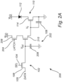
- Fig. 2A shows a pixel circuit 200.
- the pixel circuit 200 is particularly useful for analog pixel driving, but may also be used for digital driving.
- a pixel circuit 200 which may form part of a display comprised of self-emitting pixel elements, such as an AMOLED display or an AMLED display.
- the display may be an active matrix (AM) display.
- AM active matrix
- the pixel circuit 200 comprises a selection block 102, a driver-side storage element 108, and a driver block 110, and is connectable to a self-emitting pixel-element 112, such as an LED, OLED, or ⁇ LED.
- a self-emitting pixel-element 112 such as an LED, OLED, or ⁇ LED.
- the pixel circuit 200 comprises an intermediate storage block 202, connected between the selection block 102 and the driver-block 110, as will be elaborated further upon below.
- the selection block 102 is connected to a selection line SEL 104 and to a data line DATA 105.
- the selection block comprises a selection transistor 106, where a gate terminal of the selection transistor 106 is connected to the selection line 104, so that the selection transistor 106 is controlled by the selection line 104, and where a source or drain terminal of the selection transistor 106 is connected to the data line 105.
- the selection block 102 is configured to receive pixel data on the data line 105 upon assertion of the selection line 104.
- the other source or drain terminal of the selection transistor 106 is connected at a node Vint to the intermediate storage block 202, and in particular to the intermediate pixel data storage element 208.
- the present inventive concept is by no means limited to the selection block being comprised of a single selection transistor 106. Rather, other designs, for example, comprising several transistors and/or logic gates, etc., as known by the skilled person, are equally possible.
- the driver block 110 comprises a driver transistor 114 connectable in series with the self-emitting pixel element 112 between a supply voltage V DD and ground. Further, the gate terminal of the driver transistor 114 is connected to the node V x .
- the driver-side storage element 108 is in the example of Fig. 2A capacitor 108. It is connected between the node V x and ground, i.e., between the intermediate storage block 202 and the source terminal of the driver transistor 114 opposite to the self-emitting pixel element 112.
- the driver block 110 is connectable to the self-emitting pixel element 112 for driving the self-emitting pixel element 112, wherein an instantaneous brightness of the self-emitting pixel element 112 is controlled based on said driver-side pixel data storage element 108.
- the driver block 110 is connectable to the self-emitting pixel element 112 for driving the self-emitting pixel element 112, wherein an instantaneous brightness of the self-emitting pixel element 112 is controlled based on said driver-side pixel data storage element 108.
- other pixel driving arrangements as known by the skilled person are equally possible.
- the intermediate storage block 202 is connected between the selection block 102 and the driver block 110. More specifically, the intermediate storage block 202 is connected at the node V int to the selection block 102. Further, the intermediate storage block 202 is connected to the driver block 110 at the node V x .
- the intermediate storage block 202 comprises an intermediate pixel data storage element 208, a latch transistor 206 and a forwarding transistor 210.
- the intermediate pixel data storage element is a capacitor 208.
- the intermediate pixel data storage element 208 is connected at the node V int to the selection block 102, and to ground.
- the selection block 102 is configured to receive pixel data on the data line 105 upon assertion of the selection line 104, upon assertion of the selection line 104, the voltage on the data line 105 will charge the intermediate pixel data storage element 208.
- intermediate storage block 202 is connected to the driver-side pixel data storage element 108 at the node V x , and to a latch line LATCH 204.
- the intermediate storage block 202 comprises a latch transistor 206 connected at a gate terminal to the latch line 204, so that the latch line 204 controls the latch transistor 206.
- the latch transistor is at a drain terminal connected to the supply voltage V DD and at its source terminal to a drain terminal of the forwarding transistor 210.
- the gate terminal of the forwarding transistor 210 is connected to the selection block 102 and the intermediate pixel data storage element 208 through the node V int .
- the forwarding transistor 210 is controlled by the voltage present on the upper plates of the intermediate pixel data storage element 208.
- the forwarding transistor is configured as a source-follower.
- the forwarding transistor 210 is connected to the driver-side pixel data storage element 108 through the node V x .
- the pixel circuit is configured so that the pixel data input on said data line is transferred to said intermediate pixel data storage element upon assertion of the selection line 104, and so that pixel data is transferred from the intermediate pixel data storage element 208 to the driver-side pixel data storage element 108 upon assertion of the latch line 204.
- the skilled person could naturally contemplate other arrangement for configuring this functionality.
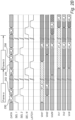
- FIG. 2B An example of operation of the pixel circuit 200 will now be exemplified with reference to the timing diagram of Fig. 2B for driving a display comprising a plurality of pixel circuits 200 of Fig. 2A .
- a method example of updating a display comprised of pixels each associated with a respective pixel circuit 200 will be disclosed. While exemplified herein for the pixel circuit 200 of Fig. 2A , the method example is equally valid, mutatis mutandis, for displays comprising the pixel circuits 300 if Fig. 3 (see below) or 400 of Fig. 4 (also see below).
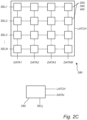
- Fig. 2C shows a display 280 comprised of pixels each associated with a respective pixel circuit 200.
- pixels may be organized in columns and rows.
- Data lines DATA1, DATA2, DATA3... DATAM may run vertically through the display, while selection lines SEL1, SEL2, SEL3... SELN may run horizontally through the display.
- selection lines SEL1, SEL2, SEL3... SELN may run horizontally through the display.
- a specific selection line selects a corresponding row of pixels in the display, while the individual pixels of that line then may be addressed through the data lines.
- each pixel circuit 200 may be connected to a same latch line LATCH.
- the pixels may be sequentially updated with respective pixel data, such as a respective analog data voltage, i.e., the voltage on the internal node V int (cf. Fig. 2A ), at the upper plate of the intermediate pixel data storage element 208 in the pixel circuit may be refreshed like in the 2T1C pixel circuit of Fig. 1A .
- pixel data may be refreshed by sequentially selecting each selection line, while applying a corresponding pixel data voltage to each data line.
- the global, i.e., common, LATCH line 204, common to each pixel circuit of the display may be activated, allowing the voltage stored in the intermediate pixel data storage element 208 to pass to the driver-side pixel data storage element 108 and driver block 110.
- the method example may be implemented in a display controller 282, connected to each data line DATAi 105, each selection line SELj 104 and the single latch line LATCH 204. Further, there may be provided a non-transitory computer-readable storage medium having stored thereon instructions for implementing the method, when executed on a device having processing capabilities.
- FIG. 2B This is exemplified for a single data line DATAi in Fig. 2B , corresponding to a specific column of pixels.
- the timing diagram is provided for reading in new data of two consecutive frames (frame a and frame b). Schematically shown are voltages on selection lines SEL1, SEL2, ..., SEL N, on nodes Vx1, Vx2, ..., VxN, i.e., the V x node of the respective pixel circuit 200, and on nodes Vint1, Vint2, ..., VintN i.e., the V int node of the respective pixel circuit 200.
- pixel data d1_a is input on the DATAi line while asserting the selection line SEL1.
- d1_a shows up on V int1 .
- other pixel data may be input on the other DATA lines (not shown in Fig. 2B ), with all pixel circuits connected to the SEL1 line forming a subset of pixel circuits in the form of a row of the display.
- asserting the selection line SEL1 is asserted for each pixel circuit in the subset of pixel circuits of the plurality of pixel circuits formed by the row.
- the procedure is repeated with pixel data d2_a while asserting the selection line SEL2 corresponding to a next row of the display, and so on.
- the pixel circuit asserting the selection line connected to the pixel in question, and inputting a pixel data voltage on the data line will result in the pixel data being provided to the respective node V int , thereby charging the intermediate pixel data storage element 208 capacitor.
- the pixel data thus input will not be immediately visible in the pixel. Instead, it is only stored in the intermediate pixel-data storage element 208, while the instantaneous brightness of the self-emitting pixel element of the respective pixel remains unchanged.
- the common LATCH line may be asserted, i.e., simultaneously, for each pixel circuit of the plurality of pixel circuits, asserting said LATCH line. This results in a simultaneous updating of all pixels.
- Fig. 3 shows a pixel circuit suitable for employing digital pixel driving.
- a pixel circuit 300 which may form part of a display comprised of self-emitting pixel elements, such as an AMOLED display or an AMLED display.
- the display may be an active matrix (AM) display.
- AM active matrix
- the pixel circuit 300 comprises a selection block 102, a driver-side storage element 108, and a driver block 110 and is connectable to a self-emitting pixel-element 112, such as an LED, OLED, or ⁇ LED. Furthermore, just as in Fig. 2A , the pixel circuit 300 comprises an intermediate storage block 202, connected between the selection block 102 and the driver-block 110, as will be elaborated further upon below.
- the selection block 102 is connected to a selection line 104 and to a data line 105.
- the selection block comprises a selection transistor 106, where a gate terminal of the selection transistor 106 is connected to the selection line 104, so that the selection transistor 106 is controlled by the selection line 104, and where a source or drain terminal of the selection transistor 106 is connected to the data line 105.
- the selection block 102 is configured to receive pixel data on the data line 105 upon assertion of the selection line 104.
- the other source or drain terminal of the selection transistor 106 is connected at a node V int to the intermediate storage block 202, and in particular to the intermediate pixel data storage element 208.
- the present inventive concept is by no means limited to the selection block being comprised of a single selection transistor 106. Rather, other designs, for example, comprising several transistors and/or logic gates, etc, as known by the skilled person, are equally possible.
- the driver block 110 comprises a driver transistor 114 connectable in series with the self-emitting pixel element 112 between a supply voltage V DD and ground. Further, the gate terminal of the driver transistor 114 is connected to the inverter 302.
- the driver-side storage element 108 is in the example of Fig. 3 a capacitor 108. It is connected between the node Vx and ground, i.e., between the intermediate storage block 202 and the source terminal of the driver transistor 114 opposite to the self-emitting pixel element 112.
- the driver block 110 is connectable to the self-emitting pixel element 112 for driving the self-emitting pixel element 112, wherein an instantaneous brightness of the self-emitting pixel element 112 is controlled based on said driver-side pixel data storage element 108.
- the driver block 110 is connectable to the self-emitting pixel element 112 for driving the self-emitting pixel element 112, wherein an instantaneous brightness of the self-emitting pixel element 112 is controlled based on said driver-side pixel data storage element 108.
- other pixel driving arrangements as known by the skilled person are equally possible.
- the intermediate storage block 202 is connected between the selection block 102 and the driver block 110. More specifically, the intermediate storage block 202 is connected at the node V int to the selection block 102. Further, the intermediate storage block 202 is connected to the driver block 110 at the node V x .
- the intermediate storage block 202 comprises an intermediate pixel data storage element 208 and a latch transistor 206.
- the intermediate pixel data storage element is a capacitor 208.
- the intermediate pixel data storage element 208 is connected at the node V int to the selection block 102, and to ground.
- the selection block 102 since the selection block 102 is configured to receive pixel data on the data line 105 upon assertion of the selection line 104, upon assertion of the selection line 104, the voltage on the data line 105 will charge the intermediate pixel data storage element 208.
- intermediate storage block 202 is connected to the driver-site pixel data storage element 108 at the node V x , and to a latch line 204.
- the latch transistor 206 is connected at its gate terminal to the latch line 204, so that the latch line 204 controls the latch transistor 206. Furthermore, the latch transistor 206 is at a source or drain terminal connected at the note V int to the selection transistor 106 of the selection block 102 and to the upper plate of the intermediate pixel data storage element 208. At the other source or drain terminal, the latch transistor 206 is connected at the node V x to the upper plate of the driver-side pixel data storage element 108 and an inverter 302. The inverter 302 is further connected to the gate terminal of the driver transistor 114, so that the driver-side pixel-data storage element 108 controls the driver transistor 114 through the inverter 302.
- the inverter 302 serves to keep the full signal swing at the driving block 110.
- This inverter could be replaced by another logic gate, such as, e.g., a buffer.
- the driver-side pixel data storage element may be connected to a logic gate, and the logic gate may be connected to the driver block.
- Another example will be given below in conjunction with Fig. 4 .
- the pixel circuit is configured so that the pixel data input on the data line is transferred to the intermediate pixel data storage element upon assertion of the selection line 104, and so that pixel data is transferred from the intermediate pixel data storage element 208 to the driver-side pixel data storage element 108 upon assertion of the latch line 204.
- the skilled person could naturally contemplate other arrangement for configuring this functionality, as known in the art.
- the pixel circuit 300 of Fig. 3 is suitable for use when the data voltage applied to the pixel is a digital voltage, e.g., when using PWM digital signals to set gray levels.
- the new data is read into the storage element like in the pixel circuit 200 of Fig. 2A , but the circuitry to allow passing the data when the latch signal is activated is different. Nevertheless, the principle as per the present inventive concept remains the same.
- Fig. 4 shows a pixel circuit 400.
- the pixel circuit 400 is identical to the pixel circuit 300 of Fig. 3 , with the exception that the inverter 302 of the pixel circuit 300 of Fig. 3 has been replaced with a NOR gate 402, which at an output is connected to the gate terminal of the driver transistor 114 of the driver block 110. Further, at one of its inputs, the NOR gate 402 is connected to the intermediate pixel data storage block 202 at the node V x . Further, a second input of the NOR gate is connected to a reset line 406.
- the inverter is replaced by another logic gate, more specifically the NOR gate, allowing both simultaneously updating digital data voltages for all pixels and resetting all pixels simultaneously.
- NAND gate instead of a NOR gate, the use of a NAND gate is equally possible, in particular in the case of using PMOS transistors.
- additional buffers, inverters, or other logical gates may be inserted in the schematics for digital driving ( Figs 3 and 4 ) to improve signal integrity.
- the latch line 204 When the latch line 204 is asserted, there will be charge redistribution between the two capacitances 108, 208 on either side of the latch transistor 206. With adequately designed capacitances, this may be manageable. Otherwise an additional buffer/inverter may be inserted, e.g. between the intermediate pixel data storage element capacitor 208 and the latch transistor 206.
- CMOS complementary metal-oxide-semiconductor
- present inventive concept is not limited to the disclosed relatively simple pixel circuits, but can also be applied to more complex pixel circuits, as contemplatable by the skilled person, within the scope of the claims.
Landscapes
- Engineering & Computer Science (AREA)
- Physics & Mathematics (AREA)
- Computer Hardware Design (AREA)
- General Physics & Mathematics (AREA)
- Theoretical Computer Science (AREA)
- Control Of Indicators Other Than Cathode Ray Tubes (AREA)
Abstract
A pixel circuit (200, 300, 400) integrable as part of a display (280), comprises a selection block (102) connected to a selection line (104) and to a data line (105) and configured to receive pixel data on said data line (105) upon assertion of said selection line (104); a driver-side pixel data storage element (108); and a driver block (110) connectable to a self-emitting pixel element (112) for driving said self-emitting pixel element (112), wherein an instantaneous brightness of said self-emitting pixel element (112) is controlled based on said driver-side pixel data storage element (108), said pixel circuit (200, 300, 400) further comprising an intermediate storage block (202) comprising an intermediate pixel data storage element (208) and connected to said selection block (102), to said driver-side pixel data storage element (108), and to a latch line (204), wherein said pixel circuit (200, 300, 400) is configured so that the pixel data input on said data line (105) is transferred to said intermediate pixel data storage element (208) upon assertion of said selection line (104), and so that pixel data is transferred from said intermediate pixel data storage element (208) to said driver-side pixel data storage element (108) upon assertion of said latch line (204).
Description
- The present inventive concept relates to a pixel circuit, a display comprising a plurality of such pixel circuits, a method of controlling the display, a display controller configured to carry out the method, and to a non-transitory computer-readable storage medium having stored thereon instructions for implementing the method.
- Displays comprising self-emitting pixel elements, such as AMOLED and AMLED displays find wide application.
- In most such displays, pixel data is refreshed, i.e., a new frame is written, through a scanning procedure wherein the new pixel data is written to the display sequentially line by line, e.g., from top to bottom of the display.
- In most displays, this is unproblematic, since neighboring lines are refreshed immediately before or after their neighboring lines, so that any artefacts from the scanning procedure is not perceivable by the human eye.
- However, there are instances where this may be problematic. For example, when tiling several display modules next to each other, the last row of one module may be located immediately next to the first row of another module. Therefore, these neighboring lines will be updated with a time difference corresponding to a full frame or sub-frame interval. This can cause undesired visual artifacts.
- Thus, there is a need for improvement in this area.
- An objective of the present inventive concept is to provide a pixel circuit allowing for a display with less temporal visual artefacts.
- According to a first aspect, there is provided a pixel circuit integrable as part of a display, said pixel circuit comprising a selection block connected to a selection line and to a data line and configured to receive pixel data on said data line upon assertion of said selection line; a driver-side pixel data storage element; and a driver block connectable to a self-emitting pixel element for driving said self-emitting pixel element, wherein an instantaneous brightness of said self-emitting pixel element is controlled based on said driver-side pixel data storage element, said pixel circuit further comprising an intermediate storage block comprising an intermediate pixel data storage element and connected to said selection block, to said driver-side pixel data storage element, and to a latch line, wherein said pixel circuit is configured so that the pixel data input on said data line is transferred to said intermediate pixel data storage element upon assertion of said selection line, and so that pixel data is transferred from said intermediate pixel data storage element to said driver-side pixel data storage element upon assertion of said latch line.
- A pixel may be associated with or comprise a single self-emitting pixel element. In another case, a pixel may comprise several sub-pixels, each associated with or comprising a respective self-emitting pixel element. For example, the respective self-emitting pixel element of each sub-pixel may emit a different primary color. For example, there may be one sub-pixel for each of the colors red, green, and blue.
- With "pixel circuit" should be understood the circuitry associated with the driving of a specific pixel or sub-pixel. Typically, a single pixel circuit may be associated with a single pixel or sub-pixel and each pixel or sub-pixel may be associated with a single pixel circuit.
- With "pixel data" should be understood data indicating an intended instantaneous brightness of the self-emitting pixel element. For example, and typically, the pixel data may be either an analog or a digital voltage. In the case of an analog voltage, increasing voltage may indicate a higher instantaneous brightness level of the self-emitting pixel element. In the case of a digital voltage, the digital voltage may indicate whether the self-emitting pixel element should be turned on or off. In this case, the self-emitting pixel element may be arranged to repeatedly turn on and off, e.g., through pulse width modulation (PWM).
- The present inventive concept stems from a realization that the arranging of an intermediate pixel data storage element allows simultaneous visual updating of all pixels of a display, instead of visual updating through scanning through the display lines. While the pixel data may still be written into the respective intermediate storage block through a scanning procedure employing the data and selection lines, the updated pixel data will only become visible and active in the respective pixel upon assertion of the latch line. By arranging for all pixel circuits in a display to be connected to a same, i.e., global latch line, and asserting that latch line, all pixels of the display may be simultaneously updated. Hereby, visual artefacts from the scanning may be eliminated.
- The present inventive concept may find further use for 3D applications, wherein the 3D effect is created using a 2D display, such as a TV, and glasses that alternatingly block the light for either the left or the right eye and where therefore instantaneous updating of a whole display may be required, so the correct eye gets the correct image.
- According to an embodiment, the intermediate storage block comprises a latch transistor controlled by the latch line. This is a particularly simple way of implementing the intermediate storage block.
- According to an embodiment, the intermediate storage block further comprises a forwarding transistor, wherein the latch transistor is connected to a supply voltage and to the forwarding transistor and the forwarding transistor is controlled by the intermediate pixel data storage element and further is connected to said driver-side pixel data storage element. Hereby, the forwarding transistor may be configured as a source-follower. This is a particularly beneficial way of implementing the intermediate storage block in case of the pixel data being an analog voltage.
- According to an embodiment, the latch transistor is connected to said intermediate pixel data storage element and to the driver-side pixel data storage element. This is a particularly simple way of implementing the intermedia storage block in case of the pixel data being a digital voltage.
- According to an embodiment, the driver-side pixel data storage element is connected to a logic gate, and said logic gate is connected to said driver block. This is a particularly robust way of implementing the intermediate storage block in case of the pixel data being a digital voltage.
- According to an embodiment, the logic gate is a buffer or inverter.
- According to an embodiment, the logic gate is a NOR gate or NAND gate connected to a reset line. This allows for both simultaneously updating digital data voltages for all pixels and resetting all pixels.
- According to an embodiment, the selection block comprises a transistor controlled by said selection line and connected to said data line and to the intermediate pixel data storage element. This is a particularly simple way of implementing the selection block.
- According to an embodiment, the driver block comprises a transistor connectable in series with the self-emitting pixel element and controlled by the driver-side pixel-data storage element. This is a particularly simple way of implementing the driver block.
- According to an embodiment, said intermediate pixel data storage element and/or said driver-side pixel data storage element is a capacitor.
- According to a second aspect, there is provided a display comprising a plurality of pixel circuits according to the first aspect.
- This aspect may generally present the same or corresponding advantages as the former aspect.
- According to a third aspect, there is provided a method of updating the display according to the second aspect, said method comprising performing a pixel data update procedure, said procedure comprising simultaneously asserting said selection line for each pixel circuit in a subset of pixel circuits of said plurality of pixel circuits while inputting pixel data on each respective data line of each pixel circuit of said subset of pixel circuits, wherein said pixel data update procedure is repeated, sequentially in time, for different subsets of said plurality of pixel circuits; and, thereafter, simultaneously, for each pixel circuit of said plurality of pixel circuits, asserting said latch line.
- This aspect may generally present the same or corresponding advantages as the former aspects.
- According to an embodiment, each said subset corresponds to a row of pixels in said display.
- According to a fourth aspect, there is provided a display controller configured to carry out the method according to the third aspect.
- This aspect may generally present the same or corresponding advantages as the former aspects.
- According to a fifth aspect, there is provided a non-transitory computer-readable storage medium having stored thereon instructions for implementing the method according to the third aspect, when executed on a device having processing capabilities.
- This aspect may generally present the same or corresponding advantages as the former aspects.
- The above, as well as additional objects, features and advantages of the present inventive concept, will be better understood through the following illustrative and non-limiting detailed description, with reference to the appended drawings. In the drawings like reference numerals will be used for like elements unless stated otherwise.
-
Fig. 1A shows, for comparison, a pixel circuit not according to the present inventive concept. -
Fig. 1B shows a timing diagram for the pixel circuit ofFig. 1A . -
Fig. 2A shows a pixel circuit. -
Fig. 2B shows a timing diagram for the pixel circuit ofFig. 2A . -
Fig. 2C shows a display comprised of pixels each associated with a respective pixel circuit. -
Fig. 3 shows a further pixel circuit. -
Fig. 4 shows a further pixel circuit. - Firstly, for comparison,
Fig. 1A illustrates apixel circuit 100 not according to the present inventive concept. - There is shown a
pixel circuit 100, which may form part of a display comprised of self-emitting pixel elements, such as an AMOLED display or an AMLED display. The display may be an active matrix (AM) display. - The
pixel circuit 100 comprises aselection block 102, a driver-side storage element 108, and adriver block 110, and is connectable to a self-emitting pixel-element 112, such as an LED, OLED, or µLED. - The
selection block 102 is connected to aselection line 104 and to adata line 105. In the shown implementation, the selection block comprises aselection transistor 106, where a gate terminal of theselection transistor 106 is connected to theselection line 104 and a source or drain terminal is connected to thedata line 105. Thereby, theselection block 102 is configured to receive pixel data on thedata line 105 upon assertion of theselection line 104. The other source or drain terminal of theselection transistor 106 is connected to the node Vx. - The
driver block 110 comprises adriver transistor 114 connectable in series with the self-emittingpixel element 112 between a supply voltage VDD and ground. Further, the gate terminal of thedriver transistor 114 is connected to the node Vx, and thus to the upper plate of thecapacitor 108, so that the driver-side pixel-data storage element 108 controls thedriver transistor 114. - The driver-
side storage element 108 is in the example ofFig. 1A acapacitor 108. It is connected between the node Vx and ground, i.e., between a source or drain terminal of theselection transistor 106 opposite to thedata line 105, and to the source terminal of thedriver transistor 114, opposite to the self-emittingpixel element 112. In other embodiments, the driver-side storage element 108 may be connected to the drain terminal of thedriver transistor 114. - Hereby, the
driver block 110 is connectable to the self-emittingpixel element 112 for driving the self-emittingpixel element 112, wherein an instantaneous brightness of the self-emittingpixel element 112 is controlled based on said driver-side pixeldata storage element 108. - In the example of
Fig. 1A , the pixel circuit is a so-called 2T1C pixel circuit, comprising twotransistors capacitor 108. -
Fig. 1B shows a timing diagram for driving a display comprising a plurality ofpixel circuits 100 ofFig. 1A . - As typical in a display, pixels may be organized in columns and rows. Data lines DATA1, DATA2, DATA3... may run vertically through the display, while selection lines SEL1, SEL2, SEL3... may run horizontally through the display. Thus, a specific selection line selects a corresponding line of pixels in the display, while the individual pixels of that line then may be addressed through the data lines.
- Thus, pixel data may be refreshed by sequentially selecting each selection line, while applying a corresponding pixel data voltage to each data line. This is exemplified for a single data line DATAi in
Fig. 1B , corresponding to a specific column of pixels. The timing diagram is provided for the updating of pixel data of two consecutive frames (frame a and frame b). Schematically shown are voltages on selection lines SEL1, SEL2, ..., SEL N and on nodes Vx1, Vx2, ..., VxN, i.e., the Vx node of the respective pixel circuit. - As can be seen, pixel data d1_a is input on the DATAi line while asserting the selection line SEL1. Hereby, d1_a shows up on Vx1. The procedure is repeated with pixel data d2_a while asserting the selection line SEL2, and so on.
- In the pixel circuit asserting the selection line connected to the pixel in question, and inputting a pixel data voltage on the data line, will result in the data voltage being provided to node Vx, thereby charging the driver-side pixel
data storage element 108 capacitor and immediately being visible in the pixel, since, in thepixel circuit 100 ofFig. 1A , the instantaneous brightness of said self-emitting pixel element of the respective pixel is controlled based on the respective driver-side pixel data storage element. Through this non-simultaneous updating, image tearing may be visible. -
Fig. 2A shows apixel circuit 200. Thepixel circuit 200 is particularly useful for analog pixel driving, but may also be used for digital driving. Similarly toFig. 1A , there is shown apixel circuit 200, which may form part of a display comprised of self-emitting pixel elements, such as an AMOLED display or an AMLED display. The display may be an active matrix (AM) display. - The
pixel circuit 200 comprises aselection block 102, a driver-side storage element 108, and adriver block 110, and is connectable to a self-emitting pixel-element 112, such as an LED, OLED, or µLED. - Furthermore, and in addition to the
pixel circuit 100 ofFig. 1A , thepixel circuit 200 comprises anintermediate storage block 202, connected between theselection block 102 and the driver-block 110, as will be elaborated further upon below. - The
selection block 102 is connected to aselection line SEL 104 and to adata line DATA 105. In the shown implementation, the selection block comprises aselection transistor 106, where a gate terminal of theselection transistor 106 is connected to theselection line 104, so that theselection transistor 106 is controlled by theselection line 104, and where a source or drain terminal of theselection transistor 106 is connected to thedata line 105. Thereby, theselection block 102 is configured to receive pixel data on thedata line 105 upon assertion of theselection line 104. - Instead of being connected directly to the node Vx (cf.
Fig. 1A ), the other source or drain terminal of theselection transistor 106 is connected at a node Vint to theintermediate storage block 202, and in particular to the intermediate pixeldata storage element 208. - It should be noted that the present inventive concept is by no means limited to the selection block being comprised of a
single selection transistor 106. Rather, other designs, for example, comprising several transistors and/or logic gates, etc., as known by the skilled person, are equally possible. - In the example of
Fig. 2A , thedriver block 110 comprises adriver transistor 114 connectable in series with the self-emittingpixel element 112 between a supply voltage VDD and ground. Further, the gate terminal of thedriver transistor 114 is connected to the node Vx. - The driver-
side storage element 108 is in the example ofFig. 2A capacitor 108. It is connected between the node Vx and ground, i.e., between theintermediate storage block 202 and the source terminal of thedriver transistor 114 opposite to the self-emittingpixel element 112. - Hereby, the
driver block 110 is connectable to the self-emittingpixel element 112 for driving the self-emittingpixel element 112, wherein an instantaneous brightness of the self-emittingpixel element 112 is controlled based on said driver-side pixeldata storage element 108. Naturally, other pixel driving arrangements as known by the skilled person are equally possible. - As mentioned above, the
intermediate storage block 202 is connected between theselection block 102 and thedriver block 110. More specifically, theintermediate storage block 202 is connected at the node Vint to theselection block 102. Further, theintermediate storage block 202 is connected to thedriver block 110 at the node Vx. - The
intermediate storage block 202 comprises an intermediate pixeldata storage element 208, alatch transistor 206 and a forwardingtransistor 210. - In the example of
Fig. 2A , the intermediate pixel data storage element is acapacitor 208. The intermediate pixeldata storage element 208 is connected at the node Vint to theselection block 102, and to ground. - Hereby, since the
selection block 102 is configured to receive pixel data on thedata line 105 upon assertion of theselection line 104, upon assertion of theselection line 104, the voltage on thedata line 105 will charge the intermediate pixeldata storage element 208. - Further, the
intermediate storage block 202 is connected to the driver-side pixeldata storage element 108 at the node Vx, and to alatch line LATCH 204. - In the example of
Fig. 2A , theintermediate storage block 202 comprises alatch transistor 206 connected at a gate terminal to thelatch line 204, so that thelatch line 204 controls thelatch transistor 206. The latch transistor is at a drain terminal connected to the supply voltage VDD and at its source terminal to a drain terminal of the forwardingtransistor 210. - The gate terminal of the forwarding
transistor 210 is connected to theselection block 102 and the intermediate pixeldata storage element 208 through the node Vint. Hereby, the forwardingtransistor 210 is controlled by the voltage present on the upper plates of the intermediate pixeldata storage element 208. Thus, the forwarding transistor is configured as a source-follower. - At a source terminal opposite to the drain terminal connected to the
latch transistor 204, the forwardingtransistor 210 is connected to the driver-side pixeldata storage element 108 through the node Vx. - Thus, through this arrangement, the pixel circuit is configured so that the pixel data input on said data line is transferred to said intermediate pixel data storage element upon assertion of the
selection line 104, and so that pixel data is transferred from the intermediate pixeldata storage element 208 to the driver-side pixeldata storage element 108 upon assertion of thelatch line 204. The skilled person could naturally contemplate other arrangement for configuring this functionality. - An example of operation of the
pixel circuit 200 will now be exemplified with reference to the timing diagram ofFig. 2B for driving a display comprising a plurality ofpixel circuits 200 ofFig. 2A . In conjunction herewith, a method example of updating a display comprised of pixels each associated with arespective pixel circuit 200 will be disclosed. While exemplified herein for thepixel circuit 200 ofFig. 2A , the method example is equally valid, mutatis mutandis, for displays comprising thepixel circuits 300 ifFig. 3 (see below) or 400 ofFig. 4 (also see below). -
Fig. 2C shows adisplay 280 comprised of pixels each associated with arespective pixel circuit 200. Just as explained above in conjunction withFig. 1B , pixels may be organized in columns and rows. Data lines DATA1, DATA2, DATA3... DATAM may run vertically through the display, while selection lines SEL1, SEL2, SEL3... SELN may run horizontally through the display. Thus, a specific selection line selects a corresponding row of pixels in the display, while the individual pixels of that line then may be addressed through the data lines. Thus, such a row corresponds to a subset of pixels in the display. Furthermore, eachpixel circuit 200 may be connected to a same latch line LATCH. - Through the respective intermediate pixel data storage blocks in each
pixel circuit 200, the pixels may be sequentially updated with respective pixel data, such as a respective analog data voltage, i.e., the voltage on the internal node Vint (cf.Fig. 2A ), at the upper plate of the intermediate pixeldata storage element 208 in the pixel circuit may be refreshed like in the 2T1C pixel circuit ofFig. 1A . Thus, in a pixel data update procedure, pixel data may be refreshed by sequentially selecting each selection line, while applying a corresponding pixel data voltage to each data line. - However, furthermore, when all data stored in intermediate pixel
data storage elements 208 of each pixel circuit has been refreshed, the global, i.e., common,LATCH line 204, common to each pixel circuit of the display may be activated, allowing the voltage stored in the intermediate pixeldata storage element 208 to pass to the driver-side pixeldata storage element 108 anddriver block 110. - The method example may be implemented in a
display controller 282, connected to eachdata line DATAi 105, eachselection line SELj 104 and the singlelatch line LATCH 204. Further, there may be provided a non-transitory computer-readable storage medium having stored thereon instructions for implementing the method, when executed on a device having processing capabilities. - This is exemplified for a single data line DATAi in
Fig. 2B , corresponding to a specific column of pixels. The timing diagram is provided for reading in new data of two consecutive frames (frame a and frame b). Schematically shown are voltages on selection lines SEL1, SEL2, ..., SEL N, on nodes Vx1, Vx2, ..., VxN, i.e., the Vx node of therespective pixel circuit 200, and on nodes Vint1, Vint2, ..., VintN i.e., the Vint node of therespective pixel circuit 200. - As can be seen, at 250, pixel data d1_a is input on the DATAi line while asserting the selection line SEL1. Hereby, d1_a shows up on Vint1. Simultaneously, other pixel data may be input on the other DATA lines (not shown in
Fig. 2B ), with all pixel circuits connected to the SEL1 line forming a subset of pixel circuits in the form of a row of the display. Thus, asserting the selection line SEL1 is asserted for each pixel circuit in the subset of pixel circuits of the plurality of pixel circuits formed by the row. - At 252, the procedure is repeated with pixel data d2_a while asserting the selection line SEL2 corresponding to a next row of the display, and so on.
- In the pixel circuit asserting the selection line connected to the pixel in question, and inputting a pixel data voltage on the data line, will result in the pixel data being provided to the respective node Vint, thereby charging the intermediate pixel
data storage element 208 capacitor. Thus, contrary to the situation with thepixel circuit 100, the pixel data thus input will not be immediately visible in the pixel. Instead, it is only stored in the intermediate pixel-data storage element 208, while the instantaneous brightness of the self-emitting pixel element of the respective pixel remains unchanged. - At 254 with all pixel data having been input for frame a, the common LATCH line may be asserted, i.e., simultaneously, for each pixel circuit of the plurality of pixel circuits, asserting said LATCH line. This results in a simultaneous updating of all pixels.
- At 256, the
above steps -
Fig. 3 shows a pixel circuit suitable for employing digital pixel driving. Similarly toFigs 1A and2A , there is shown apixel circuit 300, which may form part of a display comprised of self-emitting pixel elements, such as an AMOLED display or an AMLED display. The display may be an active matrix (AM) display. - The
pixel circuit 300 comprises aselection block 102, a driver-side storage element 108, and adriver block 110 and is connectable to a self-emitting pixel-element 112, such as an LED, OLED, or µLED. Furthermore, just as inFig. 2A , thepixel circuit 300 comprises anintermediate storage block 202, connected between theselection block 102 and the driver-block 110, as will be elaborated further upon below. - Just as in
Figs 1A and2A , theselection block 102 is connected to aselection line 104 and to adata line 105. In the shown implementation, the selection block comprises aselection transistor 106, where a gate terminal of theselection transistor 106 is connected to theselection line 104, so that theselection transistor 106 is controlled by theselection line 104, and where a source or drain terminal of theselection transistor 106 is connected to thedata line 105. Thereby, theselection block 102 is configured to receive pixel data on thedata line 105 upon assertion of theselection line 104. The other source or drain terminal of theselection transistor 106 is connected at a node Vint to theintermediate storage block 202, and in particular to the intermediate pixeldata storage element 208. - It should be noted that the present inventive concept is by no means limited to the selection block being comprised of a
single selection transistor 106. Rather, other designs, for example, comprising several transistors and/or logic gates, etc, as known by the skilled person, are equally possible. - In the example of
Fig. 3 , just as inFigs 1A and2A thedriver block 110 comprises adriver transistor 114 connectable in series with the self-emittingpixel element 112 between a supply voltage VDD and ground. Further, the gate terminal of thedriver transistor 114 is connected to theinverter 302. - The driver-
side storage element 108 is in the example ofFig. 3 acapacitor 108. It is connected between the node Vx and ground, i.e., between theintermediate storage block 202 and the source terminal of thedriver transistor 114 opposite to the self-emittingpixel element 112. - Through the above, the
driver block 110 is connectable to the self-emittingpixel element 112 for driving the self-emittingpixel element 112, wherein an instantaneous brightness of the self-emittingpixel element 112 is controlled based on said driver-side pixeldata storage element 108. Naturally, other pixel driving arrangements as known by the skilled person are equally possible. - As mentioned above, just as in
Figs 1A and2A , theintermediate storage block 202 is connected between theselection block 102 and thedriver block 110. More specifically, theintermediate storage block 202 is connected at the node Vint to theselection block 102. Further, theintermediate storage block 202 is connected to thedriver block 110 at the node Vx. - In the
pixel circuit 300 ofFig. 3 , and differently from thepixel circuit 200 ofFig. 2A , theintermediate storage block 202 comprises an intermediate pixeldata storage element 208 and alatch transistor 206. - In the example of
Fig. 3 , the intermediate pixel data storage element is acapacitor 208. The intermediate pixeldata storage element 208 is connected at the node Vint to theselection block 102, and to ground. - Hereby, as in
Figs 1A and2A , since theselection block 102 is configured to receive pixel data on thedata line 105 upon assertion of theselection line 104, upon assertion of theselection line 104, the voltage on thedata line 105 will charge the intermediate pixeldata storage element 208. - Further, the
intermediate storage block 202 is connected to the driver-site pixeldata storage element 108 at the node Vx, and to alatch line 204. - The
latch transistor 206 is connected at its gate terminal to thelatch line 204, so that thelatch line 204 controls thelatch transistor 206. Furthermore, thelatch transistor 206 is at a source or drain terminal connected at the note Vint to theselection transistor 106 of theselection block 102 and to the upper plate of the intermediate pixeldata storage element 208. At the other source or drain terminal, thelatch transistor 206 is connected at the node Vx to the upper plate of the driver-side pixeldata storage element 108 and aninverter 302. Theinverter 302 is further connected to the gate terminal of thedriver transistor 114, so that the driver-side pixel-data storage element 108 controls thedriver transistor 114 through theinverter 302. - The
inverter 302 serves to keep the full signal swing at the drivingblock 110. This inverter could be replaced by another logic gate, such as, e.g., a buffer. Thus, generally, the driver-side pixel data storage element may be connected to a logic gate, and the logic gate may be connected to the driver block. Another example will be given below in conjunction withFig. 4 . - Thus, also through this arrangement, the pixel circuit is configured so that the pixel data input on the data line is transferred to the intermediate pixel data storage element upon assertion of the
selection line 104, and so that pixel data is transferred from the intermediate pixeldata storage element 208 to the driver-side pixeldata storage element 108 upon assertion of thelatch line 204. The skilled person could naturally contemplate other arrangement for configuring this functionality, as known in the art. - The
pixel circuit 300 ofFig. 3 is suitable for use when the data voltage applied to the pixel is a digital voltage, e.g., when using PWM digital signals to set gray levels. The new data is read into the storage element like in thepixel circuit 200 ofFig. 2A , but the circuitry to allow passing the data when the latch signal is activated is different. Nevertheless, the principle as per the present inventive concept remains the same. -
Fig. 4 shows a pixel circuit 400. The pixel circuit 400 is identical to thepixel circuit 300 ofFig. 3 , with the exception that theinverter 302 of thepixel circuit 300 ofFig. 3 has been replaced with a NORgate 402, which at an output is connected to the gate terminal of thedriver transistor 114 of thedriver block 110. Further, at one of its inputs, the NORgate 402 is connected to the intermediate pixeldata storage block 202 at the node Vx. Further, a second input of the NOR gate is connected to areset line 406. - The inverter is replaced by another logic gate, more specifically the NOR gate, allowing both simultaneously updating digital data voltages for all pixels and resetting all pixels simultaneously.
- Instead of a NOR gate, the use of a NAND gate is equally possible, in particular in the case of using PMOS transistors.
- It should be noted that additional buffers, inverters, or other logical gates may be inserted in the schematics for digital driving (
Figs 3 and4 ) to improve signal integrity. When thelatch line 204 is asserted, there will be charge redistribution between the twocapacitances latch transistor 206. With adequately designed capacitances, this may be manageable. Otherwise an additional buffer/inverter may be inserted, e.g. between the intermediate pixel datastorage element capacitor 208 and thelatch transistor 206. - In the above the inventive concept has mainly been described with reference to a limited number of examples. However, as is readily appreciated by a person skilled in the art, other examples than the ones disclosed above are equally possible within the scope of the inventive concept, as defined by the appended claims.
- In particular, although this description discloses a limited number pixel circuits, it should be noted that many different embodiments are possible without going beyond the scope of the invention. For example, the scope of the present inventive concept is not limited to n-type transistor pixel circuits, but can also be applied to p-type or mixed (CMOS) transistor pixel circuits. Moreover, the present inventive concept is not limited to the disclosed relatively simple pixel circuits, but can also be applied to more complex pixel circuits, as contemplatable by the skilled person, within the scope of the claims.
Claims (15)
- A pixel circuit (200, 300, 400) integrable as part of a display (280), said pixel circuit (200, 300, 400) comprising:a selection block (102) connected to a selection line (104) and to a data line (105) and configured to receive pixel data on said data line (105) upon assertion of said selection line (104);a driver-side pixel data storage element (108); anda driver block (110) connectable to a self-emitting pixel element (112) for driving said self-emitting pixel element (112), wherein an instantaneous brightness of said self-emitting pixel element (112) is controlled based on said driver-side pixel data storage element (108),said pixel circuit (200, 300, 400) being characterized by further comprising:
an intermediate storage block (202) comprising an intermediate pixel data storage element (208) and connected to said selection block (102), to said driver-side pixel data storage element (108), and to a latch line (204), wherein said pixel circuit (200, 300, 400) is configured so that the pixel data input on said data line (105) is transferred to said intermediate pixel data storage element (208) upon assertion of said selection line (104), and so that pixel data is transferred from said intermediate pixel data storage element (208) to said driver-side pixel data storage element (108) upon assertion of said latch line (204). - The pixel circuit of claim 1, wherein said intermediate storage block (202) comprises a latch transistor (206) controlled by said latch line (204).
- The pixel circuit of claim 2, wherein said intermediate storage block (202) further comprises a forwarding transistor (210), wherein said latch transistor (206) is connected to a supply voltage and to said forwarding transistor (210) and said forwarding transistor (210) is controlled by said intermediate pixel data storage element (208) and further is connected to said driver-side pixel data storage element (108).
- The pixel circuit of claim 2, wherein said latch transistor (206) is connected to said intermediate pixel data storage element (208) and to said driver-side pixel data storage element (108).
- The pixel circuit of claim 4, wherein said driver-side pixel data storage element (108) is connected to a logic gate (302, 402), and said logic gate (302, 402) is connected to said driver block (110).
- The pixel circuit of claim 4, wherein said logic gate (302) is a buffer or inverter.
- The pixel circuit of claim 4, wherein said logic gate (402) is a NOR gate or NAND gate connected to a reset line.
- The pixel circuit of any one of claims 1-7, wherein said selection block (102) comprises a selection transistor (106) controlled by said selection line (104) and connected to said data line (105) and to said intermediate pixel data storage element (208).
- The pixel circuit of any one of claims 1-8, wherein said driver block (110) comprises a driver transistor (114) connectable in series with said self-emitting pixel element (112) and controlled by said driver-side pixel-data storage element (108).
- The pixel circuit of any one of claims 1-9, wherein said intermediate pixel data storage element (208) and/or said driver-side pixel data storage element (108) is a capacitor.
- A display (280) comprising a plurality of pixel circuits (200, 300, 400) according to any one of claims 1-10.
- A method of updating the display according to claim 11, said method comprising:performing a pixel data update procedure, said procedure comprising simultaneously asserting (250) said selection line for each pixel circuit in a subset of pixel circuits of said plurality of pixel circuits while inputting pixel data on each respective data line of each pixel circuit of said subset of pixel circuits, wherein said pixel data update procedure is repeated (252), sequentially in time, for different subsets of said plurality of pixel circuits; and, thereafter,simultaneously, for each pixel circuit of said plurality of pixel circuits, asserting (254) said latch line.
- The method of claim 12, wherein each said subset corresponds to a row of pixels in said display.
- A display controller (282) configured to carry out the method of any one of claims 12-13.
- A non-transitory computer-readable storage medium having stored thereon instructions for implementing the method according to any one of claims 12-13, when executed on a device having processing capabilities.
Priority Applications (1)
| Application Number | Priority Date | Filing Date | Title |
|---|---|---|---|
| EP21206318.4A EP4177876A1 (en) | 2021-11-03 | 2021-11-03 | Pixel circuit |
Applications Claiming Priority (1)
| Application Number | Priority Date | Filing Date | Title |
|---|---|---|---|
| EP21206318.4A EP4177876A1 (en) | 2021-11-03 | 2021-11-03 | Pixel circuit |
Publications (1)
| Publication Number | Publication Date |
|---|---|
| EP4177876A1 true EP4177876A1 (en) | 2023-05-10 |
Family
ID=78516690
Family Applications (1)
| Application Number | Title | Priority Date | Filing Date |
|---|---|---|---|
| EP21206318.4A Withdrawn EP4177876A1 (en) | 2021-11-03 | 2021-11-03 | Pixel circuit |
Country Status (1)
| Country | Link |
|---|---|
| EP (1) | EP4177876A1 (en) |
Citations (4)
| Publication number | Priority date | Publication date | Assignee | Title |
|---|---|---|---|---|
| JP2004198683A (en) * | 2002-12-18 | 2004-07-15 | Semiconductor Energy Lab Co Ltd | Display device |
| US20040196221A1 (en) * | 2003-04-07 | 2004-10-07 | Li-Wei Shih | Driving circuit for organic light emitting diode |
| US20180144682A1 (en) * | 2016-11-22 | 2018-05-24 | Google Inc. | Display panel with concurrent global illumination and next frame buffering |
| US20200020275A1 (en) * | 2018-07-10 | 2020-01-16 | Jasper Display Corp. | Emissive pixel array and self-referencing system for driving same |
-
2021
- 2021-11-03 EP EP21206318.4A patent/EP4177876A1/en not_active Withdrawn
Patent Citations (4)
| Publication number | Priority date | Publication date | Assignee | Title |
|---|---|---|---|---|
| JP2004198683A (en) * | 2002-12-18 | 2004-07-15 | Semiconductor Energy Lab Co Ltd | Display device |
| US20040196221A1 (en) * | 2003-04-07 | 2004-10-07 | Li-Wei Shih | Driving circuit for organic light emitting diode |
| US20180144682A1 (en) * | 2016-11-22 | 2018-05-24 | Google Inc. | Display panel with concurrent global illumination and next frame buffering |
| US20200020275A1 (en) * | 2018-07-10 | 2020-01-16 | Jasper Display Corp. | Emissive pixel array and self-referencing system for driving same |
Similar Documents
| Publication | Publication Date | Title |
|---|---|---|
| US9330592B2 (en) | Pixel structure and display device comprising the same | |
| US20100315403A1 (en) | Display device, method for driving the display device, and scan signal line driving circuit | |
| US11282425B2 (en) | Source driving circuit and display panel | |
| US20050041488A1 (en) | Electro-optical device, method for driving the electro-optical device, and electronic apparatus including the electro-optical device | |
| JP5834321B2 (en) | Display device and driving method thereof | |
| CN110288950B (en) | Pixel array, array substrate and display device | |
| US9589528B2 (en) | Display device | |
| KR102028587B1 (en) | Display device | |
| CN110322827B (en) | Digital driving method of display panel and display panel | |
| US11600680B2 (en) | Organic light emitting display device for prevent distortion of reference voltage | |
| JP6417608B2 (en) | Image display device and image display device driving method. | |
| KR20170107636A (en) | Method of driving display panel and display apparatus for performing the method | |
| US20080136810A1 (en) | Image Display Device, Image Display Panel, Panel Drive Device, and Method of Driving Image Display Panel | |
| KR20190017361A (en) | Gate driving circuit and Flat panel display device using the same | |
| WO2018150490A1 (en) | Liquid crystal display device | |
| KR20150005922A (en) | Electro-optical device and method for driving the same | |
| KR102416886B1 (en) | Gate driving circuit and Flat panel display device using the same | |
| KR20100006133A (en) | Display apparatus and method for driving display apparatus | |
| CN109658893B (en) | Driving method and driving device of display panel and display equipment | |
| US20210132453A1 (en) | Liquid crystal display device | |
| KR20200033564A (en) | Display Device and Driving Method Thereof | |
| WO2018099236A1 (en) | Display assembly, display device, and display control method | |
| CN112712773A (en) | Pixel circuit and display device having the same | |
| KR100524122B1 (en) | low power organic light emitting device display driving apparatus | |
| US20240153425A1 (en) | Display device and driving method thereof |
Legal Events
| Date | Code | Title | Description |
|---|---|---|---|
| PUAI | Public reference made under article 153(3) epc to a published international application that has entered the european phase |
Free format text: ORIGINAL CODE: 0009012 |
|
| STAA | Information on the status of an ep patent application or granted ep patent |
Free format text: STATUS: THE APPLICATION HAS BEEN PUBLISHED |
|
| AK | Designated contracting states |
Kind code of ref document: A1 Designated state(s): AL AT BE BG CH CY CZ DE DK EE ES FI FR GB GR HR HU IE IS IT LI LT LU LV MC MK MT NL NO PL PT RO RS SE SI SK SM TR |
|
| STAA | Information on the status of an ep patent application or granted ep patent |
Free format text: STATUS: THE APPLICATION IS DEEMED TO BE WITHDRAWN |
|
| 18D | Application deemed to be withdrawn |
Effective date: 20231111 |