EP4175428A1 - Back cover and processing method therefor, and electronic device - Google Patents
Back cover and processing method therefor, and electronic device Download PDFInfo
- Publication number
- EP4175428A1 EP4175428A1 EP22797001.9A EP22797001A EP4175428A1 EP 4175428 A1 EP4175428 A1 EP 4175428A1 EP 22797001 A EP22797001 A EP 22797001A EP 4175428 A1 EP4175428 A1 EP 4175428A1
- Authority
- EP
- European Patent Office
- Prior art keywords
- layer
- shielding part
- cover plate
- transparent cover
- film layer
- Prior art date
- Legal status (The legal status is an assumption and is not a legal conclusion. Google has not performed a legal analysis and makes no representation as to the accuracy of the status listed.)
- Granted
Links
Images




Classifications
-
- G—PHYSICS
- G02—OPTICS
- G02F—OPTICAL DEVICES OR ARRANGEMENTS FOR THE CONTROL OF LIGHT BY MODIFICATION OF THE OPTICAL PROPERTIES OF THE MEDIA OF THE ELEMENTS INVOLVED THEREIN; NON-LINEAR OPTICS; FREQUENCY-CHANGING OF LIGHT; OPTICAL LOGIC ELEMENTS; OPTICAL ANALOGUE/DIGITAL CONVERTERS
- G02F1/00—Devices or arrangements for the control of the intensity, colour, phase, polarisation or direction of light arriving from an independent light source, e.g. switching, gating or modulating; Non-linear optics
- G02F1/01—Devices or arrangements for the control of the intensity, colour, phase, polarisation or direction of light arriving from an independent light source, e.g. switching, gating or modulating; Non-linear optics for the control of the intensity, phase, polarisation or colour
- G02F1/13—Devices or arrangements for the control of the intensity, colour, phase, polarisation or direction of light arriving from an independent light source, e.g. switching, gating or modulating; Non-linear optics for the control of the intensity, phase, polarisation or colour based on liquid crystals, e.g. single liquid crystal display cells
- G02F1/133—Constructional arrangements; Operation of liquid crystal cells; Circuit arrangements
- G02F1/1333—Constructional arrangements; Manufacturing methods
- G02F1/133308—Support structures for LCD panels, e.g. frames or bezels
- G02F1/133331—Cover glasses
-
- H—ELECTRICITY
- H04—ELECTRIC COMMUNICATION TECHNIQUE
- H04M—TELEPHONIC COMMUNICATION
- H04M1/00—Substation equipment, e.g. for use by subscribers
- H04M1/02—Constructional features of telephone sets
- H04M1/0202—Portable telephone sets, e.g. cordless phones, mobile phones or bar type handsets
- H04M1/0279—Improving the user comfort or ergonomics
- H04M1/0283—Improving the user comfort or ergonomics for providing a decorative aspect, e.g. customization of casings, exchangeable faceplate
-
- C—CHEMISTRY; METALLURGY
- C23—COATING METALLIC MATERIAL; COATING MATERIAL WITH METALLIC MATERIAL; CHEMICAL SURFACE TREATMENT; DIFFUSION TREATMENT OF METALLIC MATERIAL; COATING BY VACUUM EVAPORATION, BY SPUTTERING, BY ION IMPLANTATION OR BY CHEMICAL VAPOUR DEPOSITION, IN GENERAL; INHIBITING CORROSION OF METALLIC MATERIAL OR INCRUSTATION IN GENERAL
- C23C—COATING METALLIC MATERIAL; COATING MATERIAL WITH METALLIC MATERIAL; SURFACE TREATMENT OF METALLIC MATERIAL BY DIFFUSION INTO THE SURFACE, BY CHEMICAL CONVERSION OR SUBSTITUTION; COATING BY VACUUM EVAPORATION, BY SPUTTERING, BY ION IMPLANTATION OR BY CHEMICAL VAPOUR DEPOSITION, IN GENERAL
- C23C14/00—Coating by vacuum evaporation, by sputtering or by ion implantation of the coating forming material
- C23C14/06—Coating by vacuum evaporation, by sputtering or by ion implantation of the coating forming material characterised by the coating material
- C23C14/08—Oxides
- C23C14/083—Oxides of refractory metals or yttrium
-
- C—CHEMISTRY; METALLURGY
- C23—COATING METALLIC MATERIAL; COATING MATERIAL WITH METALLIC MATERIAL; CHEMICAL SURFACE TREATMENT; DIFFUSION TREATMENT OF METALLIC MATERIAL; COATING BY VACUUM EVAPORATION, BY SPUTTERING, BY ION IMPLANTATION OR BY CHEMICAL VAPOUR DEPOSITION, IN GENERAL; INHIBITING CORROSION OF METALLIC MATERIAL OR INCRUSTATION IN GENERAL
- C23C—COATING METALLIC MATERIAL; COATING MATERIAL WITH METALLIC MATERIAL; SURFACE TREATMENT OF METALLIC MATERIAL BY DIFFUSION INTO THE SURFACE, BY CHEMICAL CONVERSION OR SUBSTITUTION; COATING BY VACUUM EVAPORATION, BY SPUTTERING, BY ION IMPLANTATION OR BY CHEMICAL VAPOUR DEPOSITION, IN GENERAL
- C23C14/00—Coating by vacuum evaporation, by sputtering or by ion implantation of the coating forming material
- C23C14/06—Coating by vacuum evaporation, by sputtering or by ion implantation of the coating forming material characterised by the coating material
- C23C14/10—Glass or silica
-
- C—CHEMISTRY; METALLURGY
- C23—COATING METALLIC MATERIAL; COATING MATERIAL WITH METALLIC MATERIAL; CHEMICAL SURFACE TREATMENT; DIFFUSION TREATMENT OF METALLIC MATERIAL; COATING BY VACUUM EVAPORATION, BY SPUTTERING, BY ION IMPLANTATION OR BY CHEMICAL VAPOUR DEPOSITION, IN GENERAL; INHIBITING CORROSION OF METALLIC MATERIAL OR INCRUSTATION IN GENERAL
- C23C—COATING METALLIC MATERIAL; COATING MATERIAL WITH METALLIC MATERIAL; SURFACE TREATMENT OF METALLIC MATERIAL BY DIFFUSION INTO THE SURFACE, BY CHEMICAL CONVERSION OR SUBSTITUTION; COATING BY VACUUM EVAPORATION, BY SPUTTERING, BY ION IMPLANTATION OR BY CHEMICAL VAPOUR DEPOSITION, IN GENERAL
- C23C14/00—Coating by vacuum evaporation, by sputtering or by ion implantation of the coating forming material
- C23C14/06—Coating by vacuum evaporation, by sputtering or by ion implantation of the coating forming material characterised by the coating material
- C23C14/14—Metallic material, boron or silicon
-
- G—PHYSICS
- G02—OPTICS
- G02F—OPTICAL DEVICES OR ARRANGEMENTS FOR THE CONTROL OF LIGHT BY MODIFICATION OF THE OPTICAL PROPERTIES OF THE MEDIA OF THE ELEMENTS INVOLVED THEREIN; NON-LINEAR OPTICS; FREQUENCY-CHANGING OF LIGHT; OPTICAL LOGIC ELEMENTS; OPTICAL ANALOGUE/DIGITAL CONVERTERS
- G02F1/00—Devices or arrangements for the control of the intensity, colour, phase, polarisation or direction of light arriving from an independent light source, e.g. switching, gating or modulating; Non-linear optics
- G02F1/01—Devices or arrangements for the control of the intensity, colour, phase, polarisation or direction of light arriving from an independent light source, e.g. switching, gating or modulating; Non-linear optics for the control of the intensity, phase, polarisation or colour
- G02F1/13—Devices or arrangements for the control of the intensity, colour, phase, polarisation or direction of light arriving from an independent light source, e.g. switching, gating or modulating; Non-linear optics for the control of the intensity, phase, polarisation or colour based on liquid crystals, e.g. single liquid crystal display cells
- G02F1/133—Constructional arrangements; Operation of liquid crystal cells; Circuit arrangements
- G02F1/1333—Constructional arrangements; Manufacturing methods
- G02F1/1334—Constructional arrangements; Manufacturing methods based on polymer dispersed liquid crystals, e.g. microencapsulated liquid crystals
-
- G—PHYSICS
- G02—OPTICS
- G02F—OPTICAL DEVICES OR ARRANGEMENTS FOR THE CONTROL OF LIGHT BY MODIFICATION OF THE OPTICAL PROPERTIES OF THE MEDIA OF THE ELEMENTS INVOLVED THEREIN; NON-LINEAR OPTICS; FREQUENCY-CHANGING OF LIGHT; OPTICAL LOGIC ELEMENTS; OPTICAL ANALOGUE/DIGITAL CONVERTERS
- G02F1/00—Devices or arrangements for the control of the intensity, colour, phase, polarisation or direction of light arriving from an independent light source, e.g. switching, gating or modulating; Non-linear optics
- G02F1/01—Devices or arrangements for the control of the intensity, colour, phase, polarisation or direction of light arriving from an independent light source, e.g. switching, gating or modulating; Non-linear optics for the control of the intensity, phase, polarisation or colour
- G02F1/13—Devices or arrangements for the control of the intensity, colour, phase, polarisation or direction of light arriving from an independent light source, e.g. switching, gating or modulating; Non-linear optics for the control of the intensity, phase, polarisation or colour based on liquid crystals, e.g. single liquid crystal display cells
- G02F1/133—Constructional arrangements; Operation of liquid crystal cells; Circuit arrangements
- G02F1/1333—Constructional arrangements; Manufacturing methods
- G02F1/1335—Structural association of cells with optical devices, e.g. polarisers or reflectors
- G02F1/133509—Filters, e.g. light shielding masks
- G02F1/133512—Light shielding layers, e.g. black matrix
-
- G—PHYSICS
- G02—OPTICS
- G02F—OPTICAL DEVICES OR ARRANGEMENTS FOR THE CONTROL OF LIGHT BY MODIFICATION OF THE OPTICAL PROPERTIES OF THE MEDIA OF THE ELEMENTS INVOLVED THEREIN; NON-LINEAR OPTICS; FREQUENCY-CHANGING OF LIGHT; OPTICAL LOGIC ELEMENTS; OPTICAL ANALOGUE/DIGITAL CONVERTERS
- G02F1/00—Devices or arrangements for the control of the intensity, colour, phase, polarisation or direction of light arriving from an independent light source, e.g. switching, gating or modulating; Non-linear optics
- G02F1/01—Devices or arrangements for the control of the intensity, colour, phase, polarisation or direction of light arriving from an independent light source, e.g. switching, gating or modulating; Non-linear optics for the control of the intensity, phase, polarisation or colour
- G02F1/15—Devices or arrangements for the control of the intensity, colour, phase, polarisation or direction of light arriving from an independent light source, e.g. switching, gating or modulating; Non-linear optics for the control of the intensity, phase, polarisation or colour based on an electrochromic effect
- G02F1/153—Constructional details
- G02F1/157—Structural association of cells with optical devices, e.g. reflectors or illuminating devices
-
- G—PHYSICS
- G02—OPTICS
- G02F—OPTICAL DEVICES OR ARRANGEMENTS FOR THE CONTROL OF LIGHT BY MODIFICATION OF THE OPTICAL PROPERTIES OF THE MEDIA OF THE ELEMENTS INVOLVED THEREIN; NON-LINEAR OPTICS; FREQUENCY-CHANGING OF LIGHT; OPTICAL LOGIC ELEMENTS; OPTICAL ANALOGUE/DIGITAL CONVERTERS
- G02F1/00—Devices or arrangements for the control of the intensity, colour, phase, polarisation or direction of light arriving from an independent light source, e.g. switching, gating or modulating; Non-linear optics
- G02F1/01—Devices or arrangements for the control of the intensity, colour, phase, polarisation or direction of light arriving from an independent light source, e.g. switching, gating or modulating; Non-linear optics for the control of the intensity, phase, polarisation or colour
- G02F1/15—Devices or arrangements for the control of the intensity, colour, phase, polarisation or direction of light arriving from an independent light source, e.g. switching, gating or modulating; Non-linear optics for the control of the intensity, phase, polarisation or colour based on an electrochromic effect
- G02F1/153—Constructional details
- G02F1/161—Gaskets; Spacers; Sealing of cells; Filling or closing of cells
-
- G—PHYSICS
- G02—OPTICS
- G02F—OPTICAL DEVICES OR ARRANGEMENTS FOR THE CONTROL OF LIGHT BY MODIFICATION OF THE OPTICAL PROPERTIES OF THE MEDIA OF THE ELEMENTS INVOLVED THEREIN; NON-LINEAR OPTICS; FREQUENCY-CHANGING OF LIGHT; OPTICAL LOGIC ELEMENTS; OPTICAL ANALOGUE/DIGITAL CONVERTERS
- G02F2201/00—Constructional arrangements not provided for in groups G02F1/00 - G02F7/00
- G02F2201/50—Protective arrangements
-
- G—PHYSICS
- G02—OPTICS
- G02F—OPTICAL DEVICES OR ARRANGEMENTS FOR THE CONTROL OF LIGHT BY MODIFICATION OF THE OPTICAL PROPERTIES OF THE MEDIA OF THE ELEMENTS INVOLVED THEREIN; NON-LINEAR OPTICS; FREQUENCY-CHANGING OF LIGHT; OPTICAL LOGIC ELEMENTS; OPTICAL ANALOGUE/DIGITAL CONVERTERS
- G02F2202/00—Materials and properties
- G02F2202/28—Adhesive materials or arrangements
Definitions
- This application relates to the field of electronic product technologies, and in particular, to a back over and a processing method thereof, and an electronic device.
- an edge of the electrochromic film layer has a cabling region, an encapsulation region, or a discoloration non-uniform region formed due to impact of moisture, oxygen, or the like.
- a shielding part configured to shield an edge part of the electrochromic film layer is usually provided at the electrochromic film layer or on a transparent cover plate of the electronic device, so as to prevent the edge part of the electrochromic film layer from being exposed.
- the shielding part is provided at the electrochromic film layer or on the transparent cover plate, when the electrochromic film layer is laminated to the transparent cover plate, air bubbles may be easily generated between the transparent cover plate and the electrochromic film layer, and consequently, a production yield of the electronic device is reduced.
- Embodiments of this application provide a back cover of an electronic device and a processing method thereof, and an electronic device, to resolve a problem that air bubbles may be easily generated between a cover plate and an electrochromic film layer when the electrochromic film layer is laminated to the cover plate.
- a first aspect of embodiments of this application provides an electronic device.
- the electronic device includes a back cover, and the back cover includes: a transparent cover plate, an electrochromic film layer, and a shielding part.
- the electrochromic film layer and the transparent cover plate are laminated.
- the shielding part is disposed between an edge part of the electrochromic film layer and the transparent cover plate, and a thickness of the shielding part is less than 4 microns.
- the thickness of the shielding part by setting the thickness of the shielding part to be less than 4 microns, a layer difference between the electrochromic film layer and the transparent cover plate can be reduced while both a shielding effect of the shielding part and surface smoothness of the shielding part are considered; and further, when the electrochromic film layer is adhered to the transparent cover plate, air bubbles between the electrochromic film layer and the transparent cover plate can be eliminated, so that difficulty of laminating the electrochromic film layer to the transparent cover plate is greatly reduced, thereby improving a production yield. In addition, an overall thickness of the back cover is reduced, thereby facilitating a lightening and thinning design of the electronic device.
- an orthographic projection that is of the edge part of the electrochromic film layer and that is on the transparent cover plate is located in an orthographic projection that is of the shielding part and that is on the transparent cover plate.
- the shielding part can effectively shield the edge part of the electrochromic film layer, to prevent the edge part of the electrochromic film layer from being exposed, thereby improving an aesthetic appearance of the electronic device.
- the electrochromic film layer further includes a middle portion surrounded by the edge part, and at least a part of an orthographic projection that is of the middle portion and that is on the transparent cover plate does not overlap the orthographic projection that is of the shielding part and that is on the transparent cover plate.
- the back cover can show a color of the middle portion, to ensure appearance expression of the back cover.
- the thickness of the shielding part is less than or equal to 1 micron.
- a layer difference between the electrochromic film layer and the transparent cover plate can be further reduced, and further, when the electrochromic film layer is adhered to the transparent cover plate, air bubbles between the electrochromic film layer and the transparent cover plate can be eliminated, so that difficulty of laminating the electrochromic film layer to the transparent cover plate is greatly reduced, thereby improving a production yield.
- an overall thickness of the back cover is further reduced, thereby further facilitating a lightening and thinning design of the electronic device.
- the thickness of the shielding part is greater than or equal to 0.01 micron.
- the thickness of the shielding part is greater than or equal to 0.01 micron, so that the shielding effect of the shielding part can be ensured, and the edge part of the electrochromic film layer is prevented from being exposed. Therefore, a layer difference between the electrochromic film layer and the transparent cover plate can be reduced while a shielding effect of the shielding part is considered, air bubbles between the electrochromic film and the transparent cover plate is eliminated, so that difficulty of laminating the electrochromic film layer to the transparent cover plate is greatly reduced, thereby improving a production yield.
- an overall thickness of the back cover is reduced, thereby facilitating a lightening and thinning design of the electronic device.
- light transmittance of the shielding part ranges from 0 to 50%. In this way, by setting the light transmittance of the shielding part to range from 0 to 50%, the shielding effect of the shielding part can be ensured, and the edge part of the electrochromic film layer is prevented from being exposed.
- the shielding part is a non-conductive layer. In this way, the shielding part can be prevented from interfering with an antenna signal of the electronic device, thereby improving stability of the antenna signal of the electronic device.
- resistance of the shielding part is greater than or equal to 5 megohms. In this way, the shielding part can be prevented from interfering with an antenna signal of the electronic device, thereby improving stability of the antenna signal of the electronic device.
- the shielding part includes a light shielding layer.
- the light shielding layer includes one or more of an indium layer, an indium alloy layer, and a first interleaved layer including at least two sub-layers of different refractive indexes that are successively and alternately laminated. Therefore, the shielding effect of the shielding part can be ensured while reducing the thickness of the shielding part, and color types of the light shielding layer can be more abundant, so that the shielding part and the back cover can be better integrated.
- the interleaved layer is a first interleaved layer including a silicon dioxide layer and a titanium dioxide layer that are successively and alternately laminated, a second interleaved layer including a silicon dioxide layer and a niobium oxide layer that are successively and alternately laminated, or a third interleaved layer including a silicon dioxide layer or a tantalum oxide layer that are successively and alternately laminated.
- both a thickness of the indium layer and a thickness of the indium alloy layer range from 10 nm to 50 nm; and a thickness of the interleaved layer ranges from 200 nm to 1000 nm.
- the shielding effect of the light shielding layer can be ensured while preventing the light shielding layer from conducting electricity, so that the light shielding layer are opaque and non-conductive, to ensure the shielding effect of the light shielding layer and avoid interference caused by the light shielding layer to the antenna signal of the electronic device.
- the thickness of the interleaved layer can range from 200 nm to 1000 nm, the shielding effect of the light shielding layer can be ensured while reducing the thickness of the shielding part, and color types of the light shielding layer can be more abundant, so that the shielding part and the back cover can be better integrated.
- the shielding part is disposed on a surface that is of the transparent cover plate and that faces the electrochromic film layer.
- the surface of the transparent cover plate is smooth and flat, so that the shielding part can be conveniently disposed on the surface of the transparent cover plate, thereby reducing processing difficulty of the shielding part, and improving processing efficiency and a production yield.
- the shielding part further includes an underlayer, and the underlayer is disposed between the light shielding layer and the transparent cover plate.
- the underlayer can improve adherence between the light shielding layer and the transparent cover plate, thereby reducing processing difficulty of the light shielding layer, and effectively preventing the light shielding layer from falling off.
- the underlayer is a silicon-containing underlayer or a zirconia-containing underlayer. Therefore, the adherence between the light shielding layer and the transparent cover plate can be increased while reducing a thickness of the underlayer, thereby reducing impact of the underlayer on the overall thickness of the shielding part.
- a thickness of the silicon-containing underlayer ranges from 1 nm to 7 nm, and a thickness of the zirconia-containing underlayer ranges from 5 nm to 30 nm. Therefore, the adherence between the light shielding layer and the transparent cover plate can be increased while reducing a thickness of the underlayer, thereby reducing impact of the underlayer on the overall thickness of the shielding part.
- the shielding part further includes a protective layer, and the protective layer is disposed on a side that is of the light shielding layer and that is away from the transparent cover plate.
- the protective layer can protect the light shielding layer, to prevent the light shielding layer from being scratched and falling off.
- the protective layer is a niobium oxide layer or a titanium oxide layer.
- the niobium oxide layer and titanium oxide layer have relatively high hardness, so that a protective effect of the protective layer can be improved.
- a thickness of the protective layer ranges from 10 nm to 35 nm. Therefore, the light shielding layer can be effectively protected by using the protective layer, and impact of the protective layer on the overall thickness of the shielding part can be reduced.
- the back cover further includes a decoration layer, and the decoration layer is disposed on a side that is of the electrochromic film layer and that is away from the transparent cover plate. Therefore, appearance expression of the back cover can be improved.
- the decoration layer includes at least one of an optical film layer, a color layer, and a texture layer. Therefore, the back cover can have various light lusters, colors, and texture changes, to improve appearance expression of the back cover.
- a color difference AEab between a color of the shielding part and a color of the decoration layer ranges from 0 to 5. Therefore, by controlling the color difference ⁇ Eab between the color of the shielding part and the color of the decoration layer to be within 0 to 5, the color of the shielding part and the color of the decoration layer can be substantially the same, thereby improving an aesthetic appearance of the back cover.
- the electronic device further includes a circuit board.
- the circuit board is located in the back cover, and the electrochromic film layer and the circuit board are electrically connected.
- a second aspect of embodiments of this application provides a back cover.
- the back cover includes: a transparent cover plate; an electrochromic film layer, and a shielding part.
- the electrochromic film layer and the transparent cover plate are laminated; and the shielding part is disposed between an edge part of the electrochromic film layer and the transparent cover plate, and a thickness of the shielding part is less than 4 microns.
- the thickness of the shielding part by setting the thickness of the shielding part to be less than 4 microns, a layer difference between the electrochromic film layer and the transparent cover plate can be reduced while both a shielding effect of the shielding part and surface smoothness of the shielding part are considered; and further, when the electrochromic film layer is adhered to the transparent cover plate, air bubbles between the electrochromic film layer and the transparent cover plate can be eliminated, so that difficulty of laminating the electrochromic film layer to the transparent cover plate is greatly reduced, thereby improving a production yield. In addition, an overall thickness of the back cover is reduced, thereby facilitating a lightening and thinning design of the electronic device.
- an orthographic projection that is of the edge part of the electrochromic film layer and that is on the transparent cover plate is located in an orthographic projection that is of the shielding part and that is on the transparent cover plate.
- the shielding part can effectively shield the edge part of the electrochromic film layer, to prevent the edge part of the electrochromic film layer from being exposed, thereby improving an aesthetic appearance of the electronic device.
- the electrochromic film layer further includes a middle portion surrounded by the edge part, and at least a part of an orthographic projection that is of the middle portion and that is on the transparent cover plate does not overlap the orthographic projection that is of the shielding part and that is on the transparent cover plate.
- the back cover can show a color of the middle portion, to ensure appearance expression of the back cover.
- the thickness of the shielding part is less than or equal to 1 micron.
- a layer difference between the electrochromic film layer and the transparent cover plate can be further reduced, and further, when the electrochromic film layer is adhered to the transparent cover plate, air bubbles between the electrochromic film layer and the transparent cover plate can be eliminated, so that difficulty of laminating the electrochromic film layer to the transparent cover plate is greatly reduced, thereby improving a production yield.
- an overall thickness of the back cover is further reduced, thereby further facilitating a lightening and thinning design of the electronic device.
- the thickness of the shielding part is greater than or equal to 0.01 micron.
- the thickness of the shielding part is greater than or equal to 0.01 micron, so that the shielding effect of the shielding part can be ensured, and the edge part of the electrochromic film layer is prevented from being exposed. Therefore, a layer difference between the electrochromic film layer and the transparent cover plate can be reduced while a shielding effect of the shielding part is considered, air bubbles between the electrochromic film and the transparent cover plate is eliminated, so that difficulty of laminating the electrochromic film layer to the transparent cover plate is greatly reduced, thereby improving a production yield.
- an overall thickness of the back cover is reduced, thereby facilitating a lightening and thinning design of the electronic device.
- light transmittance of the shielding part ranges from 0 to 50%. In this way, by setting the light transmittance of the shielding part to range from 0 to 50%, the shielding effect of the shielding part can be ensured, and the edge part of the electrochromic film layer is prevented from being exposed.
- the shielding part is a non-conductive layer. In this way, the shielding part can be prevented from interfering with an antenna signal of the electronic device, thereby improving stability of the antenna signal of the electronic device.
- resistance of the shielding part is greater than or equal to 5 megohms. In this way, the shielding part can be prevented from interfering with an antenna signal of the electronic device, thereby improving stability of the antenna signal of the electronic device.
- the shielding part includes a light shielding layer.
- the light shielding layer includes one or more of an indium layer, an indium alloy layer, and a first interleaved layer including at least two sub-layers of different refractive indexes that are successively and alternately laminated. Therefore, the shielding effect of the shielding part can be ensured while reducing the thickness of the shielding part, and color types of the light shielding layer can be more abundant, so that the shielding part and the back cover can be better integrated.
- the interleaved layer is a first interleaved layer including a silicon dioxide layer and a titanium dioxide layer that are successively and alternately laminated, a second interleaved layer including a silicon dioxide layer and a niobium oxide layer that are successively and alternately laminated, or a third interleaved layer including a silicon dioxide layer or a tantalum oxide layer that are successively and alternately laminated.
- both a thickness of the indium layer and a thickness of the indium alloy layer range from 10 nm to 50 nm; and a thickness of the interleaved layer ranges from 200 nm to 1000 nm.
- the shielding effect of the light shielding layer can be ensured while preventing the light shielding layer from conducting electricity, so that the light shielding layer are opaque and non-conductive, to ensure the shielding effect of the light shielding layer and avoid interference caused by the light shielding layer to the antenna signal of the electronic device.
- the thickness of the interleaved layer can range from 200 nm to 1000 nm, the shielding effect of the light shielding layer can be ensured while reducing the thickness of the shielding part, and color types of the light shielding layer can be more abundant, so that the shielding part and the back cover can be better integrated.
- the shielding part is disposed on a surface that is of the transparent cover plate and that faces the electrochromic film layer.
- the surface of the transparent cover plate is smooth and flat, so that the shielding part can be conveniently disposed on the surface of the transparent cover plate, thereby reducing processing difficulty of the shielding part, and improving processing efficiency and a production yield.
- the shielding part further includes an underlayer, and the underlayer is disposed between the light shielding layer and the transparent cover plate.
- the underlayer can improve adherence between the light shielding layer and the transparent cover plate, thereby reducing processing difficulty of the light shielding layer, and effectively preventing the light shielding layer from falling off.
- the underlayer is a silicon-containing underlayer or a zirconia-containing underlayer. Therefore, the adherence between the light shielding layer and the transparent cover plate can be increased while reducing a thickness of the underlayer, thereby reducing impact of the underlayer on the overall thickness of the shielding part.
- a thickness of the silicon-containing underlayer ranges from 1 nm to 7 nm, and a thickness of the zirconia-containing underlayer ranges from 5 nm to 30 nm. Therefore, the adherence between the light shielding layer and the transparent cover plate can be increased while reducing a thickness of the underlayer, thereby reducing impact of the underlayer on the overall thickness of the shielding part.
- the shielding part further includes a protective layer, and the protective layer is disposed on a side that is of the light shielding layer and that is away from the transparent cover plate.
- the protective layer can protect the light shielding layer, to prevent the light shielding layer from being scratched and falling off.
- the protective layer is a niobium oxide layer or a titanium oxide layer.
- the niobium oxide layer and titanium oxide layer have relatively high hardness, so that a protective effect of the protective layer can be improved.
- a thickness of the protective layer ranges from 10 nm to 35 nm. Therefore, the light shielding layer can be effectively protected by using the protective layer, and impact of the protective layer on the overall thickness of the shielding part can be reduced.
- the back cover further includes a decoration layer, and the decoration layer is disposed on a side that is of the electrochromic film layer and that is away from the transparent cover plate. Therefore, appearance expression of the back cover can be improved.
- the decoration layer includes at least one of an optical film layer, a color layer, and a texture layer. Therefore, the back cover can have various light lusters, colors, and texture changes, to improve appearance expression of the back cover.
- a color difference AEab between a color of the shielding part and a color of the decoration layer ranges from 0 to 5. Therefore, by controlling the color difference ⁇ Eab between the color of the shielding part and the color of the decoration layer to be within 0 to 5, the color of the shielding part and the color of the decoration layer can be substantially the same, thereby improving an aesthetic appearance of the back cover.
- a third aspect of embodiments of this application provides a screen, including a transparent cover plate, a display panel, and a shielding part.
- the display panel and the transparent cover plate are laminated.
- the shielding part is disposed between an edge part of the display panel and the transparent cover plate, and a thickness of the shielding part is less than 4 microns.
- the thickness of the shielding part by setting the thickness of the shielding part to be less than 4 microns, a layer difference between the display panel and the transparent cover plate can be reduced while both a shielding effect of the shielding part and surface smoothness of the shielding part are considered; and further, when the display panel is adhered to the transparent cover plate, air bubbles between the display panel and the transparent cover plate can be eliminated, so that difficulty of laminating the display panel to the transparent cover plate is greatly reduced, thereby improving a production yield.
- an overall thickness of the screen is reduced, thereby facilitating a lightening and thinning design of an electronic device.
- an orthographic projection that is of an edge part of an electrochromic film layer and that is on the transparent cover plate is located in an orthographic projection that is of the shielding part and that is on the transparent cover plate.
- the shielding part can effectively shield the edge part of the electrochromic film layer, to prevent the edge part of the electrochromic film layer from being exposed, thereby improving an aesthetic appearance of the electronic device.
- the thickness of the shielding part is less than 1 micron.
- the thickness of the shielding part is greater than or equal to 0.01 micron.
- a fourth aspect of embodiments of this application provides a method for processing a back cover.
- the back cover includes a transparent cover plate and an electrochromic film layer, and the electrochromic film layer and the transparent cover plate are laminated.
- the processing method includes: forming a shielding part between the transparent cover plate and an edge part of the electrochromic film layer, by using a vacuum coating process or a water electroplating process, where a thickness of the shielding part is less than 4 microns.
- the shielding part is formed by using a vacuum coating process or a water electroplating process, and the thickness of the shielding part is made to be less than 4 microns, so that a requirement for a shielding effect of the shielding part and a requirement for surface smoothness of the shielding part can be satisfied, a layer difference between the electrochromic film layer and the transparent cover plate is reduced; and further, when the electrochromic film layer is adhered to the transparent cover plate, air bubbles between the electrochromic film layer and the transparent cover plate can be eliminated, so that difficulty of laminating the electrochromic film layer to the transparent cover plate is greatly reduced, thereby improving a production yield.
- an overall thickness of the back cover is reduced, thereby facilitating a lightening and thinning design of the electronic device.
- the electrochromic film layer further includes a middle portion surrounded by the edge part, a region that is on the transparent cover plate and that is opposite to the middle portion is a second region, and before the shielding part is formed on the surface that is of the first region and that faces the edge part, the method further includes: forming a removable film layer on a surface that is of the second region and that faces the middle portion; and after a shielding part is formed on the surface that is of the first region and that faces the edge part, the method further includes: removing the removable film layer. Therefore, accuracy of a plating position of the shielding part can be improved, so that plating difficulty is reduced, thereby improving a production yield.
- first”, “second”, “third”, and “fourth” are used for descriptive purposes only, and cannot be construed as indicating or implying relative importance or implicitly indicating the quantity of technical features indicated. Therefore, the features defined with “first”, “second”, “third”, and “fourth” may explicitly or implicitly include one or more of the features.
- the term "including”, “containing” or any other variant thereof is intended to cover non-exclusive inclusion, so that a process, method, article or apparatus including a series of elements includes not only those elements, but also other elements not explicitly listed, or elements inherent to such a process, method, article or apparatus.
- the element defined by the sentence “including a... " does not exclude that other identical elements are also present in the process, method, article or apparatus including the element.
- the term "and/or" is only used to describe an association relationship between associated objects, and indicates that three relationships may exist.
- a and/or B may indicate the following: Only A exists, both A and B exist, and only B exists.
- the character "/" in the text usually indicates an "or" relationship between the associated objects.
- This application provides an electronic device, where the electronic device includes a back cover of an electrochromic function.
- this application provides an electronic device, a shielding part whose thickness is less than 4 microns is deposed between a transparent cover plate and an edge part of an electrochromic film layer, so that a layer difference between the electrochromic film layer and the transparent cover plate can be reduced while both the shielding effect of the shielding part and surface smoothness of the shielding part are considered; and further, when the electrochromic film layer is adhered to the transparent cover plate, air bubbles between the electrochromic film layer and the transparent cover plate can be eliminated, so that difficulty of laminating the electrochromic film layer to the transparent cover plate is greatly reduced, thereby improving a production yield.
- this electronic device 100 includes, but is not limited to, an electronic device 100 such as a mobile phone, a tablet personal computer (tablet personal computer), a laptop computer (laptop computer), a personal digital assistant (personal digital assistant, PDA), a personal computer, a notebook computer, a vehicle-mounted device, or a wearable device.
- an electronic device 100 such as a mobile phone, a tablet personal computer (tablet personal computer), a laptop computer (laptop computer), a personal digital assistant (personal digital assistant, PDA), a personal computer, a notebook computer, a vehicle-mounted device, or a wearable device.
- PDA personal digital assistant
- a specific form of the electronic device 100 is not limited in embodiments of this application.
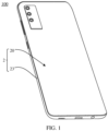
- FIG. 1 is a schematic diagram of a structure of an electronic device 100 according to some embodiments of this application.
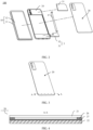
- FIG. 2 is an exploded view of an electronic device 100 in FIG. 1 >.
- the electronic device 100 is a phablet.
- the electronic device 100 includes a screen 1, a circuit board, and a back case 2.
- FIG. 1 , FIG. 2 and the following related accompanying drawings show only some example components included in the electronic device 100. An actual shape, an actual size, an actual position, and an actual configuration of these components are not limited by FIG. 1 , FIG. 2 and the following accompanying drawings. In some other embodiments, alternatively, the electronic device 100 may not include the screen 1.
- the screen 1 is configured to display an image, a video, and the like.
- the screen 1 may include a transparent cover plate and a display panel 12.
- the transparent cover plate in the screen 1 may be the front cover plate 11 shown in FIG. 2 .
- the front cover plate 11 and the display panel 12 are laminated and fixedly connected.
- the front cover plate 11 is mainly configured to protect the display panel 12 and prevent dust.
- a material of the front cover plate 11 includes, but is not limited to, glass.
- the display panel 12 may be a flexible display panel, or may be a rigid display panel.
- the display panel 12 may be an organic light-emitting diode (organic light-emitting diode, OLED) display panel, an active-matrix organic light-emitting diode or an active-matrix organic light-emitting diode (active-matrix organic light-emitting diode, AMOLED) display panel, a mini organic light-emitting diode (mini organic light-emitting diode) display panel, a micro organic light-emitting diode (micro organic light-emitting diode) display panel, a quantum dot light emitting diodes (quantum dot light emitting diodes, QLED) display panel, and a liquid crystal display (liquid crystal display, LCD).
- OLED organic light-emitting diode
- AMOLED active-matrix organic light-emitting diode
- mini organic light-emitting diode mini organic light-emitting diode
- micro organic light-emitting diode micro organic light-
- the back case 2 is configured to protect an internal electronic device of the electronic device 100.
- the back case 2 includes a frame 23 and a back cover 20.
- the back cover 20 may include a transparent cover plate 21, an electrochromic film layer 22, a shielding part 26, and a frame 23.
- the transparent cover plate 21 is located on a side that is of the display panel 12 and that is away from the front cover plate 11.
- the transparent cover plate 21, the front cover plate 11, and the display panel 12 are laminated.
- the frame 23 is located between the transparent cover plate 21 and the front cover plate 11, and the frame 23 is fastened on the transparent cover plate 21.
- the transparent cover plate 21 may be made of glass or a transparent resin material with specific hardness.
- the frame 23 may be fixedly connected to the transparent cover plate 21 by using adhesive.
- the frame 23 may alternatively be integrally formed with the transparent cover plate 21 that is, the frame 23 and the transparent cover plate 21 may be an integral structure.
- the front cover plate 11 is fastened to the frame 23.
- the front cover plate 11 may be fastened to the frame 23 by using adhesive.
- the front cover plate 11, the transparent cover plate 21, and the frame 23 enclose an internal accommodation space of the electronic device 100, and the internal accommodation space accommodates the display panel 12, the circuit board 3, and the like.
- FIG. 3 is a perspective view of a back cover 20 according to some embodiments of this application.
- FIG. 4 is a sectional view taken along a line A-A in FIG. 3 .
- An electrochromic film layer 22 and a transparent cover plate 21 are laminated. Specifically, the electrochromic film layer 22 may be located on a side that is of the transparent cover plate 21 and that faces a screen 1.
- the electrochromic film layer 22 may be adhered to an inner surface of the transparent cover plate 21 by using optically clear adhesive 27 (optically clear adhesive, OCA).
- OCA optically clear adhesive
- the inner surface of the transparent cover plate 21 is a surface that is of the transparent cover plate 21 and that is close to an inner space of an electronic device 100.
- the optically clear adhesive 27 is special adhesive for bonding a transparent optical element (such as a lens).
- the optically clear adhesive is colorless and transparent, has light transmittance greater than 90%, good bonding strength, can be cured at a room temperature or a medium temperature, and has small curing shrinkage.
- the optically transparent adhesive 27 is a special substrate-free double-sided adhesive with an optically transparent layer.
- the electrochromic film layer 22 may undergo a stable and reversible color change under an action of an applied electric field, which is shown as a reversible change in color and transparency in appearance.
- a magnitude of a voltage acting on the electrochromic film layer 22 may be changed, to change a color of the electrochromic film layer 22, so that an appearance of the electrochromic film layer 22 shows a different color.
- a magnitude of a voltage acting on the electrochromic film layer 22 may be changed, to change transparency of the electrochromic film layer 22, so that the electrochromic film layer 22 may show different appearance states such as a transparent state and a frosted state (colored state).
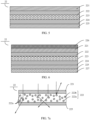
- FIG. 5 is a sectional view of an electrochromic film layer 22 of a back cover 20 according to an embodiment of this application.
- the electrochromic film layer 22 may include a first transparent conducting layer 221, an electrochromic layer 222, an electrolyte layer 223, an ion storage layer 224, and a second transparent conducting layer 225 that are laminated.
- the electrochromic film layer 22 works and the voltage is applied between the two transparent conducting layers (namely, the first transparent conducting layer 221 and the second transparent conducting layer 222), a material of the electrochromic layer 222 undergoes a redox reaction under an action of a specific voltage, and a color of the electrochromic layer 222 changes.
- the electrolyte layer 223 is used for conducting electricity.
- the ion storage layer 224 is configured to store corresponding counter ions and maintain a charge balance of an entire system when the material of the electrochromic layer 22 undergoes the redox reaction.
- the ion storage layer 224 may alternatively be made of an electrochromic material whose performance is opposite to a color change performance of the material of the preceding electrochromic layer 222, so that colors can be superimposed or complementary.
- the electrochromic layer 22 is made of an anodic oxidation color changing material
- the ion storage layer 224 can be made of a cathodic reduction color changing material.
- the first transparent conducting layer 221 and the second transparent conducting layer 225 may be made of indium tin oxide (ITO), tin oxide (SnO2), and antimony tin oxide (ATO), but are not limited thereto.
- ITO indium tin oxide
- SnO2 tin oxide
- ATO antimony tin oxide
- the electrochromic layer 222 is a core layer of the electrochromic film layer 22, and is also a layer at which color change reaction occurs.
- the material of the electrochromic layer 222 may fall into two types: an inorganic electrochromic material and an organic electrochromic material.
- the inorganic electrochromic material may be tungsten trioxide (WO3) or nickel oxide (NiO).
- the organic electrochromic material mainly includes polythiophenes and derivatives thereof, a viologen compound, a tetrathiafulvalene compound, a metal phthalocyanine compound, and the like.
- the electrolyte layer 223 is made of a special conductive material, for example, a liquid electrolyte material containing a solution of lithium perchlorate, sodium perchlorate, or the like, or may be made of a solid electrolyte material.
- the electrochromic film layer 22 in this embodiment may undergo a stable and reversible color change under an action of an applied electric field, and the technology of the electrochromic film layer 22 is mature and requires low costs.
- FIG. 6 is a sectional view of another electrochromic film layer 22 of a back cover 20 according to an embodiment of this application.
- the electrochromic film layer 22 shown in FIG. 6 further includes a first substrate layer 226 and a second substrate layer 227.
- the first substrate layer 226 is disposed on a side that is of the first transparent conducting layer 221 and that is away from the electrochromic layer 222
- the second substrate layer 227 is disposed on a side that is of the second transparent conducting layer 225 and that is away from the electrochromic layer 222.
- the first substrate layer 226 and the second substrate layer 227 may be configured to support and protect the electrochromic layer 222.
- a material of the first substrate layer 226 and the second substrate layer 227 may be glass or plastic.
- the electrochromic layer 222 can be supported and protected, so that structural stability and reliability of the electrochromic layer 222 is improved, thereby facilitating prolonging a service life of the electrochromic film layer 22, so as to reduce use costs.
- a material of the electrochromic layer 222 undergoes a redox reaction under an action of the voltage. Therefore, a color of the electrochromic layer 222 changes, so that the electrochromic film layer 22 switches between a transparent state and a colored state. It can be understood that the material of the electrochromic layer 222 and a magnitude of the voltage between the first transparent conducting layer 221 and the second transparent conducting layer 225 may be changed, to change the color of the electrochromic layer 222, so that an appearance of the back cover 20 is more diversified.
- FIG. 7a and FIG. 7b are sectional views of still another electrochromic film layer 22 of a back cover 20 according to an embodiment of this application.
- FIG. 7a shows a state when no electric field is applied to the electrochromic film layer 22.
- FIG. 7b shows a state when an electric field is applied to the electrochromic film layer 22.
- the electrochromic film layer 22 includes a first transparent conducting layer 221, an electrochromic layer 222, and a second transparent conducting layer 225.
- the electrochromic layer 222 is a polymer dispersed liquid crystal (polymer dispersed liquid crystal, PDLC) dimming film.
- the electrochromic layer 222 includes a polymer dispersed liquid crystal (PDLC) and an organic solid polymer matrix. Specifically, a liquid crystal 222a is dispersed in an organic solid polymer matrix 222b (polymer network structure) as micron-sized liquid droplets.
- PDLC polymer dispersed liquid crystal
- the liquid crystal 222a when no electric field is applied, the liquid crystal 222a is freely oriented, and a refractive index of the liquid crystal 222a does not match a refractive index of the liquid crystal 222b.
- a refractive index of the liquid crystal 222a When passing through the substrate 222b, light is strongly scattered by the liquid crystal 222a to be in an opaque opalescent or translucent state, so that the electrochromic film layer 22 has specific haze (namely, a blur rate), and the electrochromic film layer 22 is in a colored state (may also be referred to as a frosted state).
- the electric field may be applied to adjust an optical axis orientation of the liquid crystal 222a, and when the refractive index of the liquid crystal 222a matches the refractive index of the substrate 222b, the light is not scattered by the liquid crystal 222a to be in a transparent state (as shown in FIG. 7b ) when passing through the substrate 222b. Certainly, when the electric field disappears, the liquid crystal 222a returns to an original free orientation state.
- the back cover 20 can exhibit different appearance states, to implement a color change effect of the back cover 20, thereby improving appearance expression of the back cover 20.
- a decoration layer can be disposed on a side that is of the electrochromic film layer 22 and that is away from a transparent cover plate 21, so that when the electrochromic layer 222 is in the transparent state, a decoration layer 25 can be seen from outside of the transparent cover plate 21, to enable an appearance of the back cover 20 to present an appearance surface of the decoration layer 25.
- the decoration layer 25 includes at least one layer of an optical film layer, a color layer, and a texture layer. Therefore, the back cover 20 can have various light lusters, colors, and texture changes, thereby improving the appearance expression of the back cover 20.
- FIG. 8 is a top view of an electrochromic film layer 22 according to an embodiment of this application.
- the electrochromic film layer 22 is relatively sensitive to moisture and oxygen.
- an edge part 22a of the electrochromic film layer 22 is provided with an encapsulation region, to improve sealing performance of the electrochromic film layer 22.
- the edge part 22a of the electrochromic film layer 22 is uneven in color due to impact of moisture, oxygen, or the like; or the edge part of the electrochromic film layer 22 is provided with a cabling region, so that the electrochromic film layer 22 cannot exhibit a color change effect.
- the electrochromic film layer 22 further includes a middle portion 22b surrounded by the edge part 22a, and the middle portion 22b can be switched between the transparent state and the colored state.
- a shielding part 26 is disposed between the transparent cover plate 21 and the edge part 22a of the electrochromic film layer 22, to shield the edge part 22a of the electrochromic film layer 22 and prevent the edge part 22a from being exposed. In this way, the edge part 22a can be shielded by the shielding part 26, to improve an aesthetic appearance of the back cover 20.
- an orthographic projection that is of the edge part 22a and that is on a transparent cover plate 21 is located in an orthographic projection that is of the shielding part 26 and that is on the transparent cover plate 21.
- the shielding part 26 can completely cover the edge part 22a, to improve a shielding effect of the shielding part 26 and prevent the edge part 22a from being exposed, thereby further improving the aesthetic appearance of the back cover 20.
- at least a part of an orthographic projection that is of an electrochromic region 22b and that is on the transparent cover plate 21 does not overlap the orthographic projection that is of the shielding part 26 and that is on the transparent cover plate 21. In other words, the at least a part of the electrochromic region 22b is not shielded by the shielding part 26. In this way, the back cover 20 can exhibit a color of the electrochromic region 22b, to ensure appearance expression of the back cover 20.
- the shielding part 26 may shield a part of the electrochromic region 22b during actual processing, so that a part of the orthographic projection that is of the electrochromic region 22b and that is on the transparent cover plate 21 does not overlap the orthographic projection that is of the shielding part 26 and that is on the transparent cover plate 21.
- the shielding part 26 is formed by screen printing ink at the electrochromic film layer 22, and the shielding part 26 is configured to shield the edge part 22a.
- the ink is transferred on an inner surface of the transparent cover plate 21 to form the shielding part 26 for shielding the edge part 22a.
- a thickness of the shielding part 26 formed by the transferring ink or the screen printing ink is usually large.
- the thickness of the shielding part 26 formed by the screen printing ink at the electrochromic film layer shown in FIG. 9a ranges from 4 microns to 6 microns.
- the thickness of the shielding part 26 formed due to transferring ink on the inner surface of the transparent cover plate 21 shown in FIG. 11a ranges from 6 microns to 8 microns.
- the thickness of the shielding part 26 refers to a dimension that is of the shielding part 26 and that is in a direction perpendicular to the transparent cover plate 21.
- the thickness of the shielding part 26 refers to a dimension that is of the shielding part 26 and that is in a direction perpendicular to the electrochromic film layer.
- the thickness of the shielding part 26 is relatively large, a layer difference between the electrochromic film layer 22 and the transparent cover plate 21 is relatively large, and a relatively large step is formed between the electrochromic film layer 22 and the transparent cover plate 21.
- the electrochromic film layer 22 is adhered to the transparent cover plate 21 by using optically clear adhesive 27, air bubbles may be easily generated between the electrochromic film layer 22 and the transparent cover plate 21 (especially at an edge of an inner surface of the shielding part 26). Consequently, an appearance of the back cover 20 is affected, difficulty of laminating the electrochromic film layer 22 to the transparent cover plate 21 is increased, and further a production yield of the back cover 20 is affected.
- the thickness of the shielding part 26 is relatively large, the layer difference between the electrochromic film layer 22 and the transparent cover plate 21 is relatively large.
- the optically clear adhesive 27 may be easily separated from the transparent cover plate 21 under an action of stress.
- a relatively thick optically clear adhesive 27 is used to connect the electrochromic film layer 22 and the transparent cover plate 21. Consequently a thickness of the back cover 20 is increased, and further, an overall thickness of an electronic device 100 is increased, which is not conducive to implementing a lightening and thinning design of the electronic device 100.
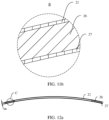
- FIG. 12a is a sectional view of a back cover 20 according to some other embodiments of this application.
- FIG. 12b is an enlarged view of a circled part C in FIG. 12a .
- a difference between the back cover 20 shown in this embodiment and the back cover 20 shown in FIG. 8 to FIG. 10 is that while both a shielding effect of the shielding part 26 and surface smoothness of the shielding part 26 are considered, a shielding part 26 for shielding an edge part 22a is disposed between a transparent cover plate 21 and the edge part 22a, so that a thickness d of the shielding part 26 is less than 4 microns.
- the thickness of the shielding part 26 may be 3.5 microns, 3 microns, 2.8 microns, 2.5 microns, 2.2 microns, 2 microns, 1.8 microns, 1.6 microns, 1.5 microns, 1.2 microns, 1 micron, or the like.
- a specific thickness of the shielding part 26 may be determined based on a material of the shielding part 26, a quantity of layers, and the like.
- the shielding part 26 may be formed between the transparent cover plate 21 and the edge part 22a of an electrochromic film layer 22 by using a vacuum coating process or a water electroplating process.
- the vacuum coating is a technology in which a physical method is used to produce a thin film material. In the vacuum coating, atoms of a material in a vacuum chamber are segregated from a heating source and hit onto a surface of an object to be plated. There are three forms of the vacuum coating: evaporation coating, sputtering coating, and ion coating.
- the water electroplating is to put a product to be electroplated into a chemical electroplating solution for electroplating.
- a film layer formed in the vacuum coating process or the water electroplating process has good compactness. Therefore, when the thickness of the shielding part 26 formed in the vacuum coating process or the water electroplating process is less than 4 microns, requirements for a shielding effect of the shielding part 26 and surface smoothness of the shielding part 26 can be satisfied.
- the thickness of the shielding part 26 is less than 4 microns, a layer difference between the electrochromic film layer 22 and the transparent cover plate 21 can be reduced on the premise that both the shielding effect of the shielding part 26 and the surface smoothness of the shielding part 26 are considered; and further, when the electrochromic film layer 22 is adhered to the transparent cover plate 21, air bubbles between the electrochromic film layer 22 and the transparent cover plate 21 can be eliminated, to greatly reduce difficulty of laminating the electrochromic film layer 22 to the transparent cover plate 21, thereby improving a production yield. In addition, an overall thickness of the back cover 20 is reduced, thereby facilitating a lightening and thinning design of an electronic device 100.
- a thickness d of the shielding part 26 is less than or equal to 1 micron.
- the thickness of the shielding part 26 may be 0.9 microns, 0.8 microns, 0.6 microns, 0.5 microns, 0.2 microns, 0.08 microns, 0.06 microns, 0.04 microns, 0.02 microns, 0.01 micron, or the like.
- the layer difference between the electrochromic film layer 22 and the transparent cover plate 21 can be further reduced, and further, when the electrochromic film layer 22 is adhered to the transparent cover plate 21, the bubbles between the electrochromic film layer 22 and the transparent cover plate 21 can be eliminated, to greatly reduce the difficulty of laminating the electrochromic film layer 22 to the transparent cover plate 21, thereby improving a production yield.
- the overall thickness of the back cover 20 is reduced, thereby further facilitating a lightening and thinning design of the electronic device 100.
- the thickness d of the shielding part 26 is greater than or equal to 0.01 micron.
- the thickness d of the shielding part 26 may satisfy 0.01 micron ⁇ d ⁇ 4 microns, or the thickness d of the shielding part 26 may satisfy 0.01 micron ⁇ d ⁇ 1 micron. In this way, by further limiting the thickness of the shielding part 26, the thickness of the shielding part 26 is greater than or equal to 0.01 micron, so that the shielding effect of the shielding part 26 can be ensured, and the edge part 22a of the electrochromic film layer 22 is prevented from being exposed.
- a layer difference between the electrochromic film layer 22 and the transparent cover plate 21 can be reduced while the shielding effect of the shielding part 26 is considered, the bubbles between the electrochromic film layer 22 and the transparent cover plate 21 can be eliminated, to greatly reduce the difficulty of laminating the electrochromic film layer 22 to the transparent cover plate 21, thereby improving a production yield.
- an overall thickness of the back cover 20 is reduced, thereby facilitating a lightening and thinning design of an electronic device 100.
- light transmittance of the shielding part 26 ranges from 0 to 50%. Further, the light transmittance of the shielding unit 26 may be 0, 10%, 15%, 20%, 25%, 30%, 35%, 40%, 45%, 50%, or the like.
- the light transmittance indicates an ability of light to pass through a medium. A greater light transmittance indicates higher translucency, and a smaller light transmittance indicates lower translucency. Therefore, by setting the light transmittance of the shielding part 26 to range from 0 to 50%, the shielding effect of the shielding part 26 can be ensured, and the edge part 22a of the electrochromic film layer 22 is prevented from being exposed.
- the shielding part 26 is a non-conductive member.
- the shielding part 26 may be an insulating member.
- resistance of the shielding part 26 is not less than 5 megohms. Specifically, the resistance of the shielding part 26 ranges from 5 megohms to 20000 megohms. In this way, the shielding part 26 can be prevented from interfering with an antenna signal of the electronic device 100, thereby improving stability of the antenna signal of the electronic device 100.
- the shielding part 26 may be disposed at any layer between the transparent cover plate 21 and the edge part 22a of the electrochromic film layer 22.
- the shielding part 26 may be disposed on a surface of a side that is of the transparent cover plate 21 and that faces the electrochromic film layer 22.
- the shielding part 26 may be disposed on a surface of a side that is of the electrochromic film layer 22 and that faces the transparent cover plate 21.
- the shielding part 26 may be disposed at a first transparent conducting layer 221 of the electrochromic film layer 22.
- the shielding part 26 may be disposed on any surface of the intermediate layer. Provided that the shielding part 26 can shield the edge part 22a of the electrochromic film layer 22, a specific position of the shielding part 26 is not limited in this application.
- the shielding part 26 is disposed on a surface that is of the transparent cover plate 21 and that faces the electrochromic film layer 22. Because the surface of the transparent cover plate 21 is smooth and flat, the shielding part 26 can be conveniently disposed on the surface of the transparent cover plate 21, thereby reducing processing difficulty of the shielding part 26, and improving processing efficiency and a production yield.
- the shielding part 26 includes a light shielding layer 26a.
- the light shielding layer 26a includes one or more of an indium layer, an indium alloy layer, and a first interleaved layer including at least two sub-layers of different refractive indexes that are successively and alternately laminated. It should be noted that "a plurality of" in this application means two or more.
- the interleaved layer may be a first interleaved layer including a silicon dioxide layer and a titanium dioxide layer that are successively and alternately laminated, a second interleaved layer including a silicon dioxide layer and a niobium oxide layer that are successively and alternately laminated, or a third interleaved layer including a silicon dioxide layer and a tantalum oxide layer that are successively and alternately laminated.
- Each sub-layer in the interleaved layer may be one or more layers, and a thickness of each sub-layer in the interleaved layer may be the same, or may be different.
- the light shielding layer 26a may include one or more of the indium layer, the indium alloy layer, and the interleaved layer.
- the light shielding layer 26a may be a laminated structure in which a plurality of the indium layer, the indium alloy layer, and the interleaved layer are laminated.
- the light shielding layer 26a is an indium layer or an indium alloy layer. Because light transmittance of the indium layer and the indium alloy layer is relatively small, and the light shielding layer 26a is disposed as the indium layer or the indium alloy layer, the thickness of the shielding part 26 may be reduced while ensuring the shielding effect of the shielding part 26.
- Both a thickness of the indium layer and a thickness of the indium alloy layer may range from 10 nm to 55 nm.
- the thickness of the indium layer or the indium alloy layer is less than 10 nm, light transmittance of the light shielding layer 26a is relatively large, and a requirement for shielding the edge part 22a of the electrochromic film layer 22 cannot be satisfied.
- the indium layer or the indium alloy layer may be conductive when the thickness of the indium layer or the indium alloy layer is greater than 55 nm.
- the shielding effect of the light shielding layer 26a can be ensured while preventing the light shielding layer 26a from conducting electricity, so that the light shielding layer 26a are opaque and non-conductive, to ensure the shielding effect of the light shielding layer 26a and avoid interference caused by the light shielding layer 26a to the antenna signal of the electronic device 100.
- the light shielding layer 26a is the interleaved layer including the at least two sub-layers of different refractive indexes that are successively and alternately laminated.
- the interleaved layer may be the first interleaved layer including the silicon dioxide layer and the titanium dioxide layer that are successively and alternately laminated, the second interleaved layer including the silicon dioxide layer and the niobium oxide layer that are successively and alternately laminated, or the third interleaved layer including the silicon dioxide layer and the tantalum oxide layer that are successively and alternately laminated.
- Each sub-layer in the interleaved layer may be one or more layers, and a thickness of each sub-layer in the interleaved layer may be the same, or may be different.
- the light shielding layer 26a is disposed as the interleaved layer including the at least two sub-layers of different refractive indexes that are successively and alternately laminated. Therefore, the light shielding layer 26a are opaque and non-conductive, and each sub-layer will reflect and refract when light passes through the light shielding layer 26a, so that the light shielding layer 26a may have more abundant appearance effects, the color types of the light shielding layer 26a can be more abundant. As a result, the shielding part 26 and the back cover 20 may be better integrated, thereby further improving the aesthetic appearance of the back cover 20.
- a thickness of the interleaved layer ranges from 200 nm to 1000 nm. Further, the thickness of the interleaved layer ranges from 200 nm to 500 nm. Specifically, the thickness of the interleaved layer may be, but is not limited to, 200 nm, 220 nm, 250 nm, 280 nm, 300 nm, 360 nm, 400 nm, 420 nm, 450 nm, 500 nm, or the like. Therefore, the shielding effect of the shielding part 26 can be ensured while reducing the thickness of the shielding part 26, and the color types of the light shielding layer 26a can be more abundant, so that the shielding part 26 and the back cover 20 can be better integrated.
- the light shielding layer 26a is a laminated structure in which the interleaved layer and the indium or indium alloy layer are laminated.
- the interleaved layer may be disposed on a side that is of the indium or indium alloy layer and this is away from the transparent cover plate 21, or may be disposed on a side that is of the indium or indium alloy layer and that is close to the transparent cover plate 21.
- the light shielding layer 26a are opaque and non-conductive, and a color of the light shielding layer 26a can be adjusted based on a need, so that the shielding part 26 and the back cover 20 can be better integrated, thereby further improving the aesthetic appearance of the back cover 20.
- the shielding part 26 further includes an underlayer 26b, and the underlayer 26b is disposed between the light shielding layer 26a and the transparent cover plate 21. That is, during processing, the underlayer 26b may be formed on the transparent cover plate 21, and then the light-shielding layer 26a may be formed on a side that is of the underlayer 26b and that is away from the transparent cover plate 21.
- the underlayer 26b can improve adherence between the light shielding layer 26a and the transparent cover plate 21, thereby reducing processing difficulty of the light shielding layer 26a, and effectively preventing the light shielding layer 26a from falling off.
- the underlayer 26b may be a silicon-containing underlayer or a zirconia-containing underlayer.
- a thickness of the silicon-containing underlayer layer may range from 1 nm to 7 nm, and therefore, the adherence between the light shielding layer 26a and the transparent cover plate 21 can be increased while reducing a thickness of the underlayer 26b, thereby reducing impact of the underlayer 26b on the overall thickness of the shielding part 26.
- the shielding part 26 further includes a protective layer 26c, and the protective layer 26c is disposed on a side that is of the light shielding layer 26a and that is away from the transparent cover plate 21.
- the protective layer 26c can protect the light shielding layer 26a, to prevent the light shielding layer 26a from being scratched and falling off.
- the protective layer 26c is an oxide layer with relatively high surface hardness.
- the protective layer 26c may be a niobium oxide layer or a titanium oxide layer. The niobium oxide layer and the titanium oxide layer have relatively high hardness, so that a protective effect of the protective layer 26c can be improved.
- the light shielding layer 26a is an indium layer or an indium alloy layer
- the light shielding layer 26a may be easily scratched by a foreign object. Consequently, an appearance and the shielding effect of the shielding part 26 are affected.
- the protective layer 26c with relatively high hardness is disposed on the side that is of the light shielding layer 26a and that is away from the light transmitting cover plate 21, so that the light shielding layer 26a can be effectively protected, thereby improving a production yield of the shielding part 26.
- a thickness of the protective layer 26c may range from 10 nm to 35 nm.
- the thickness of the protective layer 26c may be 10 nm, 15 nm, 18 nm, 20 nm, 25 nm, 30 nm, 32 nm, or the like.
- the light shielding layer 26a can be effectively protected by using the protective layer 26c, and impact of the protective layer 26c on the overall thickness of the shielding part 26 can be reduced.
- the protective layer 26c may not be disposed.
- the light shielding layer 26a may be the first interleaved layer including the silicon dioxide layer and the titanium dioxide layer that are successively and alternately laminated, the second interleaved layer including the silicon dioxide layer and the niobium oxide layer that are successively and alternately laminated, or the third interleaved layer including the silicon dioxide layer and the tantalum oxide layer that are successively and alternately laminated.
- the surface hardness of the light shielding layer 26a is relatively high, and in this case, the protective layer 26c may not be disposed on the light shielding layer 26a.
- the shielding part 26 includes the underlayer 26b, the light shielding layer 26a, and the protective layer 26c.
- the underlayer 26b may be a silicon-containing underlayer
- the light shielding layer 26a may be a light-impermeable and non-conductive indium layer or an indium alloy layer
- the protective layer 26c may be a niobium oxide layer.
- the shielding part 26 includes the underlayer 26b and the light shielding layer 26a.
- the underlayer 26b may be a zirconia-containing underlayer
- the light shielding layer 26a may be a first interleaved layer including the silicon dioxide layer and the titanium dioxide layer that are successively and alternately laminated.
- the shielding part 26 includes the underlayer 26b, two types of light shielding layers 26a, and the protective layer 26c.
- the underlayer 26b may be a zirconia-containing underlayer; the first type of light shielding layer 26a may be a first interleaved layer, a second interleaved layer, or a third interleaved layer; the second type of light shielding layer 26a may be an indium layer or an indium alloy layer; and the protective layer 26c may be a niobium oxide layer or a titanium oxide layer.
- the first type of light shielding layer 26a is disposed between the underlayer 26b and the second type of light shielding layer 26a.
- the underlayer 26b may be a silicon-containing reflective layer, and a thickness of the silicon-containing reflective layer ranges from 10 nm to 100 nm.
- FIG. 16 is a sectional view of a back cover 20 according to another embodiment of this application.
- the back cover 20 is substantially the same as the back cover 20 provided in FIG. 4 , and a difference is that the back cover 20 shown in FIG. 16 further includes a decoration layer 25, and the decoration layer 25 disposed on a side that is of an electrochromic film layer 22 and that is away from a transparent cover plate 21.
- An orthographic projection that is of the decoration layer 25 and that is on the transparent cover plate 21 completely covers an orthographic projection that is of an electrochromic region 22b of the electrochromic film layer 22 and that is on the transparent cover plate 21.
- the orthographic projection that is of the decoration layer 25 and that is on the transparent cover plate 21 and an orthographic projection that is of the electrochromic region 22b of the electrochromic layer 222 and that is on the transparent cover plate 21 are completely coincided.
- the back cover 200 may not include the decoration layer 25.
- the decoration layer 25 can be seen from outside the transparent cover plate 21, so that an appearance of the back cover 20 presents an appearance surface of the decoration layer 25.
- the decoration layer 25 includes at least one layer of an optical film layer, a color layer, and a texture layer. Therefore, the back cover 20 can have various light lusters, colors, and texture changes, thereby improving the appearance expression of the back cover 20.
- the decoration layer 25 includes the optical film layer.
- the optical film layer is an optical medium material layer that propagates light through an interface of the optical film layer. Reflection and refraction of light passing through the optical film layer can be changed, so that the decoration layer 25 exhibits a specific gloss change, for example, exhibits different color gloss at different angles, and exhibits a metal texture.
- a material, a thickness, and a quantity of layers of the optical film layer may be changed, to change reflectivity, a refractive index, and light transmittance of the optical film layer, so as to satisfy requirements in different scenarios.
- the material of the optical film layer may be an inorganic substance, or may be an organic substance.
- the inorganic substance includes at least one of metal element, inorganic oxide, and inorganic fluoride.
- the organic substance includes at least one of polyether, polyester, fluoropolymer, and silicon-containing polymer. If the material of the optical film layer is an organic substance, the optical film layer has good flexibility and bendability, and can be cut to obtain an optical film layer of a desired size.
- the material of the optical film layer includes at least one of metal element, inorganic oxide, and inorganic fluoride.
- the inorganic oxide includes at least one of metal oxide and non-metal oxide.
- the metal element may be, but is not limited to, aluminum, yttrium, germanium, or the like;
- the inorganic oxide may be, but is not limited to, titanium dioxide, trititanium pentoxide, silicon dioxide, silicon monoxide, zirconium dioxide, aluminum oxide, tantalum pentoxide, or niobium monoxide;
- the inorganic fluoride may be, but is not limited to, magnesium fluoride, calcium fluoride, or the like.
- the thickness of the optical film layer ranges from 20 nm to 500 nm.
- the thickness of the optical film layer ranges from 50 nm to 420 nm.
- the thickness of the optical film layer may be, but is not limited to, 80 nm, 95 nm, 180 nm, 250 nm, 300 nm, 360 nm, 400 nm, or the like.
- the optical film layer may be a single-layer film structure or a multilayer film structure. If the optical film layer is a multilayer film structure, by controlling a material and thickness of each layer and cooperation between layers, a required function can be implemented.
- the optical film layer includes at least two optical films of different refractive indexes that are successively and alternately laminated. In other words, when the optical film layer includes a plurality of optical films, refractive indexes of adjacent optical films are different. Further, the optical film layers are formed by at least two films of different refractive indexes that are periodically, successively and alternately laminated. Materials and thicknesses of the plurality of optical films may be the same, or may be different. Optical properties of the plurality of optical films are different. After light passes through the plurality of optical films, a surface of each optical film reflects and refracts, resulting in more abundant appearance effects.
- the thickness of the optical film ranges from 3 nm to 200 nm.
- the optical film layer may include, but is not limited to, optical films of 2 layers, 3 layers, 4 layers, 5 layers, 6 layers, 7 layers, or 8 layers.
- the decoration layer 25 includes the color layer. It can be understood that the color layer may provide abundant visual effects to the decoration layer 25. Optionally, a thickness of the color layer ranges from 50 nm to 500 nm. In an embodiment, the color layer may be formed through screen printing and spraying color ink.
- the decoration layer 25 includes the texture layer. It can be understood that the appearance surface of the decoration layer 25 is provided with the texture layer, to exhibit a plurality of appearance expressions, for example, pattern effects such as a line, a texture, or a pattern may be exhibited. Optionally, a thickness of the texture layer ranges from 100 nm to 1000 nm.
- the texture layer is formed at the decoration layer 25 by using a UV transfer optical texture process.
- the texture layer is formed at the decoration layer 25 by using high scratch resistance UV transfer adhesive, high hardness UV transfer adhesive, high elasticity UV transfer adhesive, or general-purpose UV transfer adhesive.
- the decoration layer 25 includes at least two or three of the optical film layer, the color layer, and the texture layer, to improve the appearance effect of the decoration layer 25.
- a superposition of the optical film layer and the color layer may make color expression more significant, and lusters at different angles may be different; a superposition of the optical film layer and the texture layer can make the visual effect of the texture layer more prominent, and lusters at different angles are different; a superposition of the color layer and the texture layer may exhibit a color texture; and a superposition of the optical film layer, the color layer, and the texture layer exhibits a color texture, and lusters at different angles are different.
- a color difference ⁇ Eab between a color of the shielding part 26 and a color of the decoration layer 25 ranges from 0 to 5.
- the color difference ⁇ Eab satisfies 0 ⁇ ⁇ Eab ⁇ 5
- ⁇ Eab satisfies 0 ⁇ ⁇ Eab ⁇ 2.
- the color difference is almost invisible when observed with a naked eye. Therefore, by controlling the color difference ⁇ Eab between the color of the shielding part 26 and the color of the decoration layer 25 to be within 0 to 5, the color of the shielding part 26 and the color of the decoration layer 25 can be substantially the same, thereby improving an aesthetic appearance of the back cover 20.
- L represents brightness, which ranges from 0 to 100, the lowest brightness is 0, and highest brightness is 100
- a is a color change from green to red, which ranges from -128 to +128, pure green is negative 128, pure red is positive 128, and there are 256 grades between pure green and pure red
- b is a color change from blue to yellow, which ranges from -128 to +128, pure blue is negative 128, pure yellow is positive 128, and there are 256 levels between pure blue and pure yellow.
- color samples 1 are separately calibrated as follows: color sample 1 is calibrated as L1, a1, and b1; and color sample 2 is calibrated as L2, a2, and b2.
- a circuit board 3 may include a primary circuit board 31 and a secondary circuit board 32.
- the circuit board 3 may alternatively include only the primary circuit board 31.
- the primary circuit board 31 is configured to integrate a control chip.
- the control chip may be, for example, an application processor (application processor, AP), a double data rate synchronous dynamic random access memory (double data rate, DDR) and a universal flash storage (universal flash storage, UFS).
- the primary circuit board 31 and an electrochromic film layer 22 are electrically connected.
- the primary circuit board 31 may be a rigid printed circuit board 3, may be a flexible printed circuit board 3, or may be a flexible-rigid printed circuit board 3.
- the primary circuit board 31 may be an FR-4 dielectric board, may be a Rogers dielectric board, may be an FR-4 + Rogers mixed dielectric board, or the like.
- FR-4 is a flame-resistant material grade code
- the Rogers dielectric board is a high frequency board.
- the secondary circuit board 32 is used to integrate electronic devices such as a radio frequency front end of an antenna (such as a 5G antenna), a universal serial bus (universal serial bus, USB) device, or an oscillator.
- an antenna such as a 5G antenna
- a universal serial bus universal serial bus, USB
- the secondary circuit board 32 may be a rigid printed circuit board 3, may be a flexible printed circuit board 3, or may be a flexible-rigid printed circuit board 3.
- the secondary circuit board 32 may be an FR-4 dielectric board, may be a Rogers dielectric board, may be an FR-4 + Rogers mixed dielectric board, or the like.
- connection structure 4 may be a flexible printed circuit board 3 (flexible printed circuit, FPC). In other embodiments, a connection structure 4 may alternatively be a conductor or an enamelled wire.
- the electronic device 100 further includes a middle plate 24.
- the middle plate 24 is fastened to a circumference of an inner surface of the frame 23.
- the middle plate 24 may be fastened on the frame 23 through welding, or the middle plate 24 may be integrally formed with the frame 23.
- the middle plate 24 is used as a "skeleton" of a structure of the electronic device 100, and a circuit board may be fastened on the middle plate 24 through screwing, clamping, welding, or the like.
- the circuit board 3 may be fastened, through screwing, snapping, soldering, or the like, on a surface that is of a display panel 12 and that faces a transparent cover plate 21.
- a thickness of a shielding part 26 is less than 4 microns, so that a layer difference between the electrochromic film layer 22 and the transparent cover plate 21 can be reduced while both a shielding effect of the shielding part 26 and surface smoothness of the shielding part 26 are considered; and further, when the electrochromic film layer 22 is adhered to the transparent cover plate 21, air bubbles between the electrochromic film layer 22 and the transparent cover plate 21 can be eliminated, to greatly reduce difficulty of laminating the electrochromic film layer 22 to the transparent cover plate 21, thereby improving a production yield.
- an overall thickness of the back cover 20 is reduced, thereby facilitating a lightening and thinning design of an electronic device 100.
- the electronic device 100 provided in this embodiment of this application includes the back cover 20 described in the forgoing embodiment, so that both can resolve a same technical problem and achieve a same effect.
- Some embodiments of this application further provide a screen 1, where the screen 1 includes a transparent cover plate, the display panel 12, and the shielding part 26.
- the transparent cover plate in the screen 1 may be the front cover plate 11 shown in FIG. 2 .
- the display panel 12 and the transparent cover plate are laminated.
- the display panel 12 may be located on a side that is of the transparent cover plate and that faces the back cover 20.
- the display panel 12 may be adhered to the transparent cover plate by using optically clear adhesive 27.
- the shielding part 26 is disposed between an edge part of the display panel 12 and the transparent cover plate; an orthographic projection that is of the edge part of the display panel 12 and that is on the transparent cover plate is located in an orthographic projection that is of the shielding part 26 and that is on the transparent cover plate; and a thickness d of the shielding part 26 is less than 4 microns.
- the thickness of the shielding part 26 may be 3.5 microns, 3 microns, 2.8 microns, 2.5 microns, 2.2 microns, 2 microns, 1.8 microns, 1.6 microns, 1.5 microns, 1.2 microns, 1 micron, or the like.
- a specific thickness of the shielding part 26 may be determined based on a material of the shielding part 26, a quantity of layers, and the like.
- the shielding part 26 may be formed between the transparent cover plate and the edge part of the display panel 12 by using a vacuum coating process or a water electroplating process.
- the thickness of the shielding part 26 is less than 4 microns, the layer difference between the display panel 12 and the transparent cover plate can be reduced while both the shielding effect of the shielding part 26 and the surface smoothness of the shielding part 26 are considered; and further, when the display panel 12 is adhered to the transparent cover plate, air bubbles between the display panel 12 and the transparent cover plate can be eliminated, to greatly reduce the difficulty of laminating the display panel 12 to the transparent cover plate, thereby improving the production yield.
- the overall thickness of the screen 1 is reduced, thereby facilitating the lightening and thinning design of the electronic device 100.
- the thickness d of the shielding part 26 is less than or equal to 1 micron.
- the thickness of the shielding part 26 may be 0.9 microns, 0.8 microns, 0.6 microns, 0.5 microns, 0.2 microns, 0.08 microns, 0.06 microns, 0.04 microns, 0.02 microns, 0.01 micron, or the like.
- the layer difference between the display panel 12 and the transparent cover plate can be further reduced, and further, when the display panel 12 is adhered to the transparent cover plate, the bubbles between the electrochromic film layer 22 and the transparent cover plate can be eliminated, to greatly reduce the difficulty of laminating the display panel 12 to the transparent cover plate, thereby improving the production yield.
- the overall thickness of the screen 1 is reduced, thereby further facilitating the lightening and thinning design of the electronic device 100.
- the thickness d of the shielding part 26 is greater than or equal to 0.01 micron. Specifically, the thickness d of the shielding part 26 may satisfy 0.01 micron ⁇ d ⁇ 4 microns, or the thickness d of the shielding part 26 may satisfy 0.01 micron ⁇ d ⁇ 1 micron. In this way, by further limiting the thickness of the shielding part 26, the thickness of the shielding part 26 is greater than or equal to 0.01 micron, so that the shielding effect of the shielding part 26 can be ensured, and the edge part of the display panel 12 is prevented from being exposed.
- the layer difference between the display panel 12 and the transparent cover plate can be reduced while the shielding effect of the shielding part 26 is considered, the bubbles between the display panel 12 and the transparent cover plate can be eliminated, to greatly reduce the difficulty of laminating the display panel 12 to the transparent cover plate, thereby improving a production yield.
- the overall thickness of the screen 1 is reduced, thereby facilitating the lightening and thinning design of the electronic device 100.
- An embodiment of this application further provides a method for processing a back cover 20.
- the back cover 20 includes a transparent cover plate 21 and an electrochromic film layer 22, and the electrochromic film layer 22 and the transparent cover plate 21 are laminated.
- the back cover 20 in this embodiment may be the back cover 20 in the forgoing embodiment, but is not limited thereto.
- the method includes: forming a shielding part 26 between the transparent cover plate 21 and an edge part 22a of the electrochromic film layer 22 by using a vacuum coating process or a water electroplating process, where a thickness d of the shielding part 26 satisfies d ⁇ 4 microns.
- an orthographic projection that is of the edge part 22a of the electrochromic film layer 22 and that is on the transparent cover plate 21 is located in an orthographic projection that is of the shielding part 26 and that is on the transparent cover plate 21.
- the shielding part 26 can completely cover the edge part 22a, to improve a shielding effect of the shielding part 26 and prevent the edge part 22a from being exposed, thereby further improving the aesthetic appearance of the back cover 20.
- the vacuum coating is a technology for producing a thin film material by using a physical method.
- atoms of a material in a vacuum chamber are segregated from a heating source and hit onto a surface of an object to be plated.
- the water electroplating is to put a product to be electroplated into a chemical electroplating solution for electroplating.
- a film layer formed in the vacuum coating process or the water electroplating process has good compactness.
- the thickness of the shielding part 26 formed in the vacuum coating process or the water electroplating process is less than 4 microns, requirements for a shielding effect of the shielding part 26 and surface smoothness of the shielding part 26 can be satisfied. Therefore, a layer difference between the electrochromic film layer 22 and the transparent cover plate 21 can be reduced, and further, when the electrochromic film layer 22 is adhered to the transparent cover plate 21, air bubbles between the electrochromic film layer 22 and the transparent cover plate 21 can be eliminated, to greatly reduce difficulty of laminating the electrochromic film layer 22 to the transparent cover plate 21, thereby improving a production yield. In addition, an overall thickness of the back cover 20 is reduced, thereby facilitating a lightening and thinning design of an electronic device 100.
- the shielding part 26 may be disposed at any layer between the transparent cover plate 21 and the edge part 22a of the electrochromic film layer 22.
- the shielding part 26 may be disposed on a surface of a side that is of the transparent cover plate 21 and that faces the electrochromic film layer 22.
- the shielding part 26 may be disposed on a surface of a side that is of the electrochromic film layer 22 and that faces the transparent cover plate 21.
- the shielding part 26 may be disposed on any surface of the intermediate layer.
- a specific position of the shielding part 26 is not limited in this application.
- a region that is on the transparent cover plate 21 and that is opposite to the edge part 22a of the electrochromic film layer 22 is a first region. That the shielding part 26 is formed between the transparent cover plate 21 and the edge part 22a includes: forming the shielding part 26 on a surface that is of the first region and that faces the edge part 22a, and positioning the shielding part 26 between the first region and the edge part 22a.
- the region that is on the transparent cover plate 21 and that is opposite to the edge part 22a is a region in which an orthographic projection that is of the edge part 22a and that is on the transparent cover plate 21 is located.
- the edge part 22a can be shielded by the shielding part 26 that is formed in the first region, thereby improving the aesthetic appearance of the back cover 20.
- a surface of the transparent cover plate 21 is smooth and flat, so that the shielding part 26 can be conveniently formed on the transparent cover plate 21, thereby reducing processing difficulty of the shielding part 26, and improving production efficiency and a production yield.
- the electrochromic film layer 22 further includes a middle portion 22b surrounded by the edge part 22a, and a region that is on the transparent cover plate 21 and that is opposite to the middle portion 22b is a second region; and before the shielding part 26 is formed on the surface that is of the first region and that faces the edge part 22a, the method further includes:
- the region that is on the transparent cover plate 21 and that is opposite to the electrochromic region 22b is a region in which an orthographic projection that is of the electrochromic region 22b and that is on the transparent cover plate 21 is located.
- the removable film layer may be plated or affixed on the second region before the shielding part 26 is formed on the first region, and the removable film layer may be removed after the shielding part 26 is formed on the first region on the transparent cover plate 21.
- the shielding part 26 is disposed on the surface of the side that is of the transparent cover plate 21 and that faces the electrochromic film layer 22.
- a method for processing a back cover 20 in this embodiment includes step S101 to S105.
- the electrochromic film layer 22 is of a sandwich structure, upper and lower layers of the electrochromic film layer 22 are a first transparent conducting layer 221 and a second transparent conducting layer 225, respectively, a surface of a side of the first transparent conducting layer 221 is covered with a first substrate layer 226, a surface of a side of the second transparent conducting layer 225 is covered with a second substrate layer 227, and an electrochromic layer 222 may be a PDLC dimming film.
- two transparent conducting layers on two sides of the PDLC dimming film and the PDLC dimming film may be sequentially laminated after precise alignment is performed in a roll-to-roll method, and then UV-curing is performed on a laminated structure, to obtain the electrochromic film layer 22.
- the decoration layer 25 with optically clear adhesive 27 is adhered to the second substrate layer 227 of the electrochromic film layer 22, where the decoration layer 25 may include one or more of an optical film layer, a texture layer, and a color layer.
- the optically clear adhesive 27 ranging from 15 microns to 30 microns is laminated to the first substrate layer 226 of the electrochromic film layer 22.
- S104 Form a shielding part 26 on a surface that is of the first region on the transparent cover plate 21 and that faces an edge part 22a of the electrochromic film layer 22.
- the shielding part 26 is plated (for example, vacuum coating) on the surface that is of the first region on the transparent cover plate 21 and that faces the edge part 22a of the electrochromic film layer 22.
- the shielding part 26 may include an underlayer 26b, a light shielding layer 26a, and a protective layer 26c. Specifically, in a plating process, the underlayer 26b may be first plated on the surface that is of the first region and that faces the edge part 22a of the electrochromic film layer 22.
- the underlayer 26b may be a silicon-containing underlayer 26b, and a thickness of the silicon-containing underlayer 26b ranges from 1 nm to 7 nm.
- the light shielding layer 26a is plated on a surface of a side that is of the underlayer 26b and that is away from the transparent cover plate 21.
- the light shielding layer 26a may be an indium layer or an indium alloy layer.
- the indium layer or the indium alloy layer is opaque and non-conductive, and a thickness of the indium layer or the indium alloy layer ranges from 10 nm to 55 nm.
- the protective layer 26c is plated on a surface of a side that is of the light shielding layer 26a and that is away from the underlayer 26b.
- the protective layer 26c may be an oxide layer such as a niobium oxide layer or a titanium oxide layer, and a thickness of the protective layer 26c ranges from 10 nm to 35 nm.
- a removable film layer may be plated or affixed on a surface that is of the second region on the transparent cover plate 21 and that faces an electrochromic region 22b before plating the shielding part 26, and the removable film layer may be removed after the shielding part 26 is plated on the first region.
- a method for processing a back cover 20 in this embodiment is substantially the same as the processing method in Embodiment 1, and a difference is that a material of a shielding part 26 in this embodiment is different.
- the shielding part 26 in this embodiment includes an underlayer 26b and a light shielding layer 26a.
- the underlayer 26b is a zirconia-containing underlayer, and a thickness of the zirconia-containing underlayer ranges from 5 nm to 30 nm.
- the light shielding layer 26a is a first interleaved layer including a silicon dioxide layer and a titanium dioxide layer that are successively and alternately laminated.
- the underlayer 26b is first plated on a surface that is of a first region on the transparent cover plate 21 and that faces an edge part 22a of an electrochromic film layer 22, and the underlayer 26b is a silicon-containing underlayer. Then the light shielding layer 26a is plated on a side that is of the underlayer 26b and that is away from the transparent cover plate 21.
- a method for processing a back cover in this embodiment is substantially the same as the processing method in Embodiment 1, and a difference is that a material of a shielding part 26 in this embodiment is different.
- the shielding part 26 in this embodiment includes an underlayer 26b, two types of light shielding layers 26a, and a protective layer 26c.
- the underlayer 26b is a zirconia-containing underlayer, and a thickness of the zirconia-containing underlayer ranges from 5 nm to 30 nm.
- the first type of light shielding layer is a first interleaved layer including a silicon dioxide layer and a titanium dioxide layer that are successively and alternately laminated, a second interleaved layer including a silicon dioxide layer and a niobium oxide layer that are successively and alternately laminated, or a third interleaved layer including a silicon dioxide layer or a tantalum oxide layer that are successively and alternately laminated. Thicknesses of the first interleaved layer, the second interleaved layer, and the third interleaved layer range from 200 nm to 1000 nm.
- the second type of light shielding layer is located on a side that is of the first light type of shielding layer and that is away from the underlayer 26b, and the second type of light shielding layer is an indium layer or an indium alloy layer.
- a thickness of the indium layer or the indium alloy layer ranges from 10 nm to 55 nm.
- the protective layer 26c is an oxide layer such as a niobium oxide layer or a titanium oxide layer, and a thickness of the protective layer 26c ranges from 10 nm to 35 nm.
- the underlayer 26b is first plated on a surface that is of a first region on a transparent cover 21 and that faces an edge part 22a of an electrochromic film layer 22, then the first type of light-shielding layer is plated on a surface of a side that is of the underlayer 26b and that is away from the transparent cover 21; next, the second type of light-shielding layer is plated on a surface of a side that is of the first light-shielding layer and that is away from the underlayer 26b; and finally, the protective layer 26c is plated on a surface of a side that is of the second light-shielding layer and that is away from the underlayer 26b.
- a method for processing a back cover 20 in this embodiment is substantially the same as the processing method in Embodiment 3, and a difference is that a material of a shielding part 26 in this embodiment is different.
- a shielding part 26 in this embodiment includes an underlayer 26b, two types of light shielding layers 26a, and a protective layer 26c.
- the underlayer 26b is a silicon-containing reflective layer, and a thickness of the silicon-containing reflective layer ranges from 10 nm to 100 nm.
- the first type of light shielding layer is a first interleaved layer including a silicon dioxide layer and a titanium dioxide layer that are successively and alternately laminated, and a thickness of the first interleaved layer ranges from 200 nm to 1000 nm.
- the second type of light shielding layer is located on a side that is of the first light type of shielding layer and that is away from the underlayer 26b, and the second type of light shielding layer is an indium layer or an indium alloy layer.
- a thickness of the indium layer or the indium alloy layer ranges from 10 nm to 55 nm.
- the protective layer 26c is an oxide layer such as a niobium oxide layer or a titanium oxide layer, and a thickness of the protective layer 26c ranges from 10 nm to 35 nm.
- An electronic device 100 provided in this application includes a back cover 20 with an electrochromic function.
- a state of an electrochromic film layer 22 can be manually switched based on an actual need, to switch an appearance state of the back cover 22.
- the user may switch the state of the electrochromic film layer 22 by using a volume key, a power key, or tapping the back cover, to switch the electrochromic film layer 22 between a transparent state and a frosted state (also referred to as a colored state), so that the back cover 20 exhibits different appearance states.
- the user may switch the state of the electrochromic film layer 22 based on light intensity in an actual use scenario. Specifically, the user may switch the electrochromic film 22 to the frosted state in a bright (for example, daytime) use environment, and switch the electrochromic film 22 to the transparent state in a dark (for example, nighttime) use environment. Certainly, the user may also switch the electrochromic film 22 to the transparent state in the bright (for example, the daytime) use environment, and switch the electrochromic film 22 to the frosted state in the dark (for example, the nighttime) use environment.
- a bright for example, daytime
- a dark for example, nighttime
- the user may also switch the electrochromic film 22 to the transparent state in the bright (for example, the daytime) use environment, and switch the electrochromic film 22 to the frosted state in the dark (for example, the nighttime) use environment.
- the user may switch the state of the electrochromic film layer 22 when the electronic device 100 is awakened (for example, when there is an incoming call alert, a short message alert, an alarm alert, a missed call, unread information, or the like) and when the electronic device 100 enters a standby state, by setting a program of the electronic device 100.
- a processor of the electronic device 100 may apply a voltage to the electrochromic film layer 22, so that the electrochromic film layer 22 is in a transparent state.
- the processor may cancel the voltage applied to the electrochromic film layer 22, so that the electrochromic film layer 22 is in the frosted state.
- the user may be alerted that the electronic device 100 is awakened, by switching the appearance state of the back cover, so that the user can receive a message, an incoming call, and the like in a timely manner.
Landscapes
- Physics & Mathematics (AREA)
- Chemical & Material Sciences (AREA)
- Nonlinear Science (AREA)
- Optics & Photonics (AREA)
- General Physics & Mathematics (AREA)
- Engineering & Computer Science (AREA)
- Mechanical Engineering (AREA)
- Organic Chemistry (AREA)
- Mathematical Physics (AREA)
- Crystallography & Structural Chemistry (AREA)
- Metallurgy (AREA)
- Materials Engineering (AREA)
- Chemical Kinetics & Catalysis (AREA)
- Dispersion Chemistry (AREA)
- Signal Processing (AREA)
- Laminated Bodies (AREA)
- Electrochromic Elements, Electrophoresis, Or Variable Reflection Or Absorption Elements (AREA)
Abstract
Description
- This application claims priority to
Chinese Patent Application No. 202110999310.9, filed with the China National Intellectual Property Administration on August 28, 2021 - This application relates to the field of electronic product technologies, and in particular, to a back over and a processing method thereof, and an electronic device.
- In a related technology, in an electronic device with a back cover of an electrochromic film layer, an edge of the electrochromic film layer has a cabling region, an encapsulation region, or a discoloration non-uniform region formed due to impact of moisture, oxygen, or the like. To improve an aesthetic appearance of the electronic device, a shielding part configured to shield an edge part of the electrochromic film layer is usually provided at the electrochromic film layer or on a transparent cover plate of the electronic device, so as to prevent the edge part of the electrochromic film layer from being exposed. However, after the shielding part is provided at the electrochromic film layer or on the transparent cover plate, when the electrochromic film layer is laminated to the transparent cover plate, air bubbles may be easily generated between the transparent cover plate and the electrochromic film layer, and consequently, a production yield of the electronic device is reduced.
- Embodiments of this application provide a back cover of an electronic device and a processing method thereof, and an electronic device, to resolve a problem that air bubbles may be easily generated between a cover plate and an electrochromic film layer when the electrochromic film layer is laminated to the cover plate.
- To achieve the forgoing objective, embodiments of this application use the following technical solutions.
- A first aspect of embodiments of this application provides an electronic device. The electronic device includes a back cover, and the back cover includes: a transparent cover plate, an electrochromic film layer, and a shielding part. The electrochromic film layer and the transparent cover plate are laminated. The shielding part is disposed between an edge part of the electrochromic film layer and the transparent cover plate, and a thickness of the shielding part is less than 4 microns.
- In the electronic device provided in this application, by setting the thickness of the shielding part to be less than 4 microns, a layer difference between the electrochromic film layer and the transparent cover plate can be reduced while both a shielding effect of the shielding part and surface smoothness of the shielding part are considered; and further, when the electrochromic film layer is adhered to the transparent cover plate, air bubbles between the electrochromic film layer and the transparent cover plate can be eliminated, so that difficulty of laminating the electrochromic film layer to the transparent cover plate is greatly reduced, thereby improving a production yield. In addition, an overall thickness of the back cover is reduced, thereby facilitating a lightening and thinning design of the electronic device.
- In a possible implementation of the first aspect, an orthographic projection that is of the edge part of the electrochromic film layer and that is on the transparent cover plate is located in an orthographic projection that is of the shielding part and that is on the transparent cover plate. In this way, the shielding part can effectively shield the edge part of the electrochromic film layer, to prevent the edge part of the electrochromic film layer from being exposed, thereby improving an aesthetic appearance of the electronic device.
- In a possible implementation of the first aspect, the electrochromic film layer further includes a middle portion surrounded by the edge part, and at least a part of an orthographic projection that is of the middle portion and that is on the transparent cover plate does not overlap the orthographic projection that is of the shielding part and that is on the transparent cover plate. In this way, the back cover can show a color of the middle portion, to ensure appearance expression of the back cover.
- In a possible implementation of the first aspect, the thickness of the shielding part is less than or equal to 1 micron. In this way, a layer difference between the electrochromic film layer and the transparent cover plate can be further reduced, and further, when the electrochromic film layer is adhered to the transparent cover plate, air bubbles between the electrochromic film layer and the transparent cover plate can be eliminated, so that difficulty of laminating the electrochromic film layer to the transparent cover plate is greatly reduced, thereby improving a production yield. In addition, an overall thickness of the back cover is further reduced, thereby further facilitating a lightening and thinning design of the electronic device.
- In a possible implementation of the first aspect, the thickness of the shielding part is greater than or equal to 0.01 micron. In this way, by further limiting the thickness of the shielding part, the thickness of the shielding part is greater than or equal to 0.01 micron, so that the shielding effect of the shielding part can be ensured, and the edge part of the electrochromic film layer is prevented from being exposed. Therefore, a layer difference between the electrochromic film layer and the transparent cover plate can be reduced while a shielding effect of the shielding part is considered, air bubbles between the electrochromic film and the transparent cover plate is eliminated, so that difficulty of laminating the electrochromic film layer to the transparent cover plate is greatly reduced, thereby improving a production yield. In addition, an overall thickness of the back cover is reduced, thereby facilitating a lightening and thinning design of the electronic device.
- In a possible implementation of the first aspect, light transmittance of the shielding part ranges from 0 to 50%. In this way, by setting the light transmittance of the shielding part to range from 0 to 50%, the shielding effect of the shielding part can be ensured, and the edge part of the electrochromic film layer is prevented from being exposed.
- In a possible implementation of the first aspect, the shielding part is a non-conductive layer. In this way, the shielding part can be prevented from interfering with an antenna signal of the electronic device, thereby improving stability of the antenna signal of the electronic device.
- In a possible implementation of the first aspect, resistance of the shielding part is greater than or equal to 5 megohms. In this way, the shielding part can be prevented from interfering with an antenna signal of the electronic device, thereby improving stability of the antenna signal of the electronic device.
- In a possible implementation of the first aspect, the shielding part includes a light shielding layer. The light shielding layer includes one or more of an indium layer, an indium alloy layer, and a first interleaved layer including at least two sub-layers of different refractive indexes that are successively and alternately laminated. Therefore, the shielding effect of the shielding part can be ensured while reducing the thickness of the shielding part, and color types of the light shielding layer can be more abundant, so that the shielding part and the back cover can be better integrated. In a possible implementation of the first aspect, the interleaved layer is a first interleaved layer including a silicon dioxide layer and a titanium dioxide layer that are successively and alternately laminated, a second interleaved layer including a silicon dioxide layer and a niobium oxide layer that are successively and alternately laminated, or a third interleaved layer including a silicon dioxide layer or a tantalum oxide layer that are successively and alternately laminated.
- In a possible implementation of the first aspect, both a thickness of the indium layer and a thickness of the indium alloy layer range from 10 nm to 50 nm; and a thickness of the interleaved layer ranges from 200 nm to 1000 nm.
- Therefore, by setting the thickness of the indium layer and the thickness of the indium alloy layer to range from 10 nm to 55 nm, the shielding effect of the light shielding layer can be ensured while preventing the light shielding layer from conducting electricity, so that the light shielding layer are opaque and non-conductive, to ensure the shielding effect of the light shielding layer and avoid interference caused by the light shielding layer to the antenna signal of the electronic device. By setting the thickness of the interleaved layer to range from 200 nm to 1000 nm, the shielding effect of the light shielding layer can be ensured while reducing the thickness of the shielding part, and color types of the light shielding layer can be more abundant, so that the shielding part and the back cover can be better integrated.
- In a possible implementation of the first aspect, the shielding part is disposed on a surface that is of the transparent cover plate and that faces the electrochromic film layer. The surface of the transparent cover plate is smooth and flat, so that the shielding part can be conveniently disposed on the surface of the transparent cover plate, thereby reducing processing difficulty of the shielding part, and improving processing efficiency and a production yield.
- In a possible implementation of the first aspect, the shielding part further includes an underlayer, and the underlayer is disposed between the light shielding layer and the transparent cover plate. The underlayer can improve adherence between the light shielding layer and the transparent cover plate, thereby reducing processing difficulty of the light shielding layer, and effectively preventing the light shielding layer from falling off.
- In a possible implementation of the first aspect, the underlayer is a silicon-containing underlayer or a zirconia-containing underlayer. Therefore, the adherence between the light shielding layer and the transparent cover plate can be increased while reducing a thickness of the underlayer, thereby reducing impact of the underlayer on the overall thickness of the shielding part.
- In a possible implementation of the first aspect, a thickness of the silicon-containing underlayer ranges from 1 nm to 7 nm, and a thickness of the zirconia-containing underlayer ranges from 5 nm to 30 nm. Therefore, the adherence between the light shielding layer and the transparent cover plate can be increased while reducing a thickness of the underlayer, thereby reducing impact of the underlayer on the overall thickness of the shielding part.
- In a possible implementation of the first aspect, the shielding part further includes a protective layer, and the protective layer is disposed on a side that is of the light shielding layer and that is away from the transparent cover plate. The protective layer can protect the light shielding layer, to prevent the light shielding layer from being scratched and falling off.
- In a possible implementation of the first aspect, the protective layer is a niobium oxide layer or a titanium oxide layer. The niobium oxide layer and titanium oxide layer have relatively high hardness, so that a protective effect of the protective layer can be improved.
- In a possible implementation of the first aspect, a thickness of the protective layer ranges from 10 nm to 35 nm. Therefore, the light shielding layer can be effectively protected by using the protective layer, and impact of the protective layer on the overall thickness of the shielding part can be reduced.
- In a possible implementation of the first aspect, the back cover further includes a decoration layer, and the decoration layer is disposed on a side that is of the electrochromic film layer and that is away from the transparent cover plate. Therefore, appearance expression of the back cover can be improved.
- In a possible implementation of the first aspect, the decoration layer includes at least one of an optical film layer, a color layer, and a texture layer. Therefore, the back cover can have various light lusters, colors, and texture changes, to improve appearance expression of the back cover.
- In a possible implementation of the first aspect, a color difference AEab between a color of the shielding part and a color of the decoration layer ranges from 0 to 5. Therefore, by controlling the color difference ΔEab between the color of the shielding part and the color of the decoration layer to be within 0 to 5, the color of the shielding part and the color of the decoration layer can be substantially the same, thereby improving an aesthetic appearance of the back cover.
- In a possible implementation of the first aspect, the electronic device further includes a circuit board. The circuit board is located in the back cover, and the electrochromic film layer and the circuit board are electrically connected.
- A second aspect of embodiments of this application provides a back cover. The back cover includes: a transparent cover plate; an electrochromic film layer, and a shielding part. The electrochromic film layer and the transparent cover plate are laminated; and the shielding part is disposed between an edge part of the electrochromic film layer and the transparent cover plate, and a thickness of the shielding part is less than 4 microns.
- In the back cover provided in this application, by setting the thickness of the shielding part to be less than 4 microns, a layer difference between the electrochromic film layer and the transparent cover plate can be reduced while both a shielding effect of the shielding part and surface smoothness of the shielding part are considered; and further, when the electrochromic film layer is adhered to the transparent cover plate, air bubbles between the electrochromic film layer and the transparent cover plate can be eliminated, so that difficulty of laminating the electrochromic film layer to the transparent cover plate is greatly reduced, thereby improving a production yield. In addition, an overall thickness of the back cover is reduced, thereby facilitating a lightening and thinning design of the electronic device.
- In a possible implementation of the second aspect, an orthographic projection that is of the edge part of the electrochromic film layer and that is on the transparent cover plate is located in an orthographic projection that is of the shielding part and that is on the transparent cover plate. In this way, the shielding part can effectively shield the edge part of the electrochromic film layer, to prevent the edge part of the electrochromic film layer from being exposed, thereby improving an aesthetic appearance of the electronic device.
- In a possible implementation of the second aspect, the electrochromic film layer further includes a middle portion surrounded by the edge part, and at least a part of an orthographic projection that is of the middle portion and that is on the transparent cover plate does not overlap the orthographic projection that is of the shielding part and that is on the transparent cover plate. In this way, the back cover can show a color of the middle portion, to ensure appearance expression of the back cover.
- In a possible implementation of the second aspect, the thickness of the shielding part is less than or equal to 1 micron. In this way, a layer difference between the electrochromic film layer and the transparent cover plate can be further reduced, and further, when the electrochromic film layer is adhered to the transparent cover plate, air bubbles between the electrochromic film layer and the transparent cover plate can be eliminated, so that difficulty of laminating the electrochromic film layer to the transparent cover plate is greatly reduced, thereby improving a production yield. In addition, an overall thickness of the back cover is further reduced, thereby further facilitating a lightening and thinning design of the electronic device.
- In a possible implementation of the second aspect, the thickness of the shielding part is greater than or equal to 0.01 micron. In this way, by further limiting the thickness of the shielding part, the thickness of the shielding part is greater than or equal to 0.01 micron, so that the shielding effect of the shielding part can be ensured, and the edge part of the electrochromic film layer is prevented from being exposed. Therefore, a layer difference between the electrochromic film layer and the transparent cover plate can be reduced while a shielding effect of the shielding part is considered, air bubbles between the electrochromic film and the transparent cover plate is eliminated, so that difficulty of laminating the electrochromic film layer to the transparent cover plate is greatly reduced, thereby improving a production yield. In addition, an overall thickness of the back cover is reduced, thereby facilitating a lightening and thinning design of the electronic device.
- In a possible implementation of the second aspect, light transmittance of the shielding part ranges from 0 to 50%. In this way, by setting the light transmittance of the shielding part to range from 0 to 50%, the shielding effect of the shielding part can be ensured, and the edge part of the electrochromic film layer is prevented from being exposed.
- In a possible implementation of the second aspect, the shielding part is a non-conductive layer. In this way, the shielding part can be prevented from interfering with an antenna signal of the electronic device, thereby improving stability of the antenna signal of the electronic device.
- In a possible implementation of the second aspect, resistance of the shielding part is greater than or equal to 5 megohms. In this way, the shielding part can be prevented from interfering with an antenna signal of the electronic device, thereby improving stability of the antenna signal of the electronic device.
- In a possible implementation of the second aspect, the shielding part includes a light shielding layer. The light shielding layer includes one or more of an indium layer, an indium alloy layer, and a first interleaved layer including at least two sub-layers of different refractive indexes that are successively and alternately laminated. Therefore, the shielding effect of the shielding part can be ensured while reducing the thickness of the shielding part, and color types of the light shielding layer can be more abundant, so that the shielding part and the back cover can be better integrated. In a possible implementation of the second aspect, the interleaved layer is a first interleaved layer including a silicon dioxide layer and a titanium dioxide layer that are successively and alternately laminated, a second interleaved layer including a silicon dioxide layer and a niobium oxide layer that are successively and alternately laminated, or a third interleaved layer including a silicon dioxide layer or a tantalum oxide layer that are successively and alternately laminated.
- In a possible implementation of the second aspect, both a thickness of the indium layer and a thickness of the indium alloy layer range from 10 nm to 50 nm; and a thickness of the interleaved layer ranges from 200 nm to 1000 nm.
- Therefore, by setting the thickness of the indium layer and the thickness of the indium alloy layer to range from 10 nm to 55 nm, the shielding effect of the light shielding layer can be ensured while preventing the light shielding layer from conducting electricity, so that the light shielding layer are opaque and non-conductive, to ensure the shielding effect of the light shielding layer and avoid interference caused by the light shielding layer to the antenna signal of the electronic device. By setting the thickness of the interleaved layer to range from 200 nm to 1000 nm, the shielding effect of the light shielding layer can be ensured while reducing the thickness of the shielding part, and color types of the light shielding layer can be more abundant, so that the shielding part and the back cover can be better integrated.
- In a possible implementation of the second aspect, the shielding part is disposed on a surface that is of the transparent cover plate and that faces the electrochromic film layer. The surface of the transparent cover plate is smooth and flat, so that the shielding part can be conveniently disposed on the surface of the transparent cover plate, thereby reducing processing difficulty of the shielding part, and improving processing efficiency and a production yield.
- In a possible implementation of the second aspect, the shielding part further includes an underlayer, and the underlayer is disposed between the light shielding layer and the transparent cover plate The underlayer can improve adherence between the light shielding layer and the transparent cover plate, thereby reducing processing difficulty of the light shielding layer, and effectively preventing the light shielding layer from falling off.
- In a possible implementation of the second aspect, the underlayer is a silicon-containing underlayer or a zirconia-containing underlayer. Therefore, the adherence between the light shielding layer and the transparent cover plate can be increased while reducing a thickness of the underlayer, thereby reducing impact of the underlayer on the overall thickness of the shielding part.
- In a possible implementation of the second aspect, a thickness of the silicon-containing underlayer ranges from 1 nm to 7 nm, and a thickness of the zirconia-containing underlayer ranges from 5 nm to 30 nm. Therefore, the adherence between the light shielding layer and the transparent cover plate can be increased while reducing a thickness of the underlayer, thereby reducing impact of the underlayer on the overall thickness of the shielding part.
- In a possible implementation of the second aspect, the shielding part further includes a protective layer, and the protective layer is disposed on a side that is of the light shielding layer and that is away from the transparent cover plate. The protective layer can protect the light shielding layer, to prevent the light shielding layer from being scratched and falling off.
- In a possible implementation of the second aspect, the protective layer is a niobium oxide layer or a titanium oxide layer. The niobium oxide layer and titanium oxide layer have relatively high hardness, so that a protective effect of the protective layer can be improved.
- In a possible implementation of the second aspect, a thickness of the protective layer ranges from 10 nm to 35 nm. Therefore, the light shielding layer can be effectively protected by using the protective layer, and impact of the protective layer on the overall thickness of the shielding part can be reduced.
- In a possible implementation of the second aspect, the back cover further includes a decoration layer, and the decoration layer is disposed on a side that is of the electrochromic film layer and that is away from the transparent cover plate. Therefore, appearance expression of the back cover can be improved.
- In a possible implementation of the second aspect, the decoration layer includes at least one of an optical film layer, a color layer, and a texture layer. Therefore, the back cover can have various light lusters, colors, and texture changes, to improve appearance expression of the back cover.
- In a possible implementation of the first aspect, a color difference AEab between a color of the shielding part and a color of the decoration layer ranges from 0 to 5. Therefore, by controlling the color difference ΔEab between the color of the shielding part and the color of the decoration layer to be within 0 to 5, the color of the shielding part and the color of the decoration layer can be substantially the same, thereby improving an aesthetic appearance of the back cover.
- A third aspect of embodiments of this application provides a screen, including a transparent cover plate, a display panel, and a shielding part. The display panel and the transparent cover plate are laminated. The shielding part is disposed between an edge part of the display panel and the transparent cover plate, and a thickness of the shielding part is less than 4 microns.
- In the screen provided in this application, by setting the thickness of the shielding part to be less than 4 microns, a layer difference between the display panel and the transparent cover plate can be reduced while both a shielding effect of the shielding part and surface smoothness of the shielding part are considered; and further, when the display panel is adhered to the transparent cover plate, air bubbles between the display panel and the transparent cover plate can be eliminated, so that difficulty of laminating the display panel to the transparent cover plate is greatly reduced, thereby improving a production yield. In addition, an overall thickness of the screen is reduced, thereby facilitating a lightening and thinning design of an electronic device.
- In a possible implementation of the third aspect, an orthographic projection that is of an edge part of an electrochromic film layer and that is on the transparent cover plate is located in an orthographic projection that is of the shielding part and that is on the transparent cover plate. In this way, the shielding part can effectively shield the edge part of the electrochromic film layer, to prevent the edge part of the electrochromic film layer from being exposed, thereby improving an aesthetic appearance of the electronic device.
- In a possible implementation of the third aspect, the thickness of the shielding part is less than 1 micron.
- In a possible implementation of the third aspect, the thickness of the shielding part is greater than or equal to 0.01 micron.
- A fourth aspect of embodiments of this application provides a method for processing a back cover. The back cover includes a transparent cover plate and an electrochromic film layer, and the electrochromic film layer and the transparent cover plate are laminated. The processing method includes: forming a shielding part between the transparent cover plate and an edge part of the electrochromic film layer, by using a vacuum coating process or a water electroplating process, where a thickness of the shielding part is less than 4 microns.
- In the method for processing a back cover provided in this application, the shielding part is formed by using a vacuum coating process or a water electroplating process, and the thickness of the shielding part is made to be less than 4 microns, so that a requirement for a shielding effect of the shielding part and a requirement for surface smoothness of the shielding part can be satisfied, a layer difference between the electrochromic film layer and the transparent cover plate is reduced; and further, when the electrochromic film layer is adhered to the transparent cover plate, air bubbles between the electrochromic film layer and the transparent cover plate can be eliminated, so that difficulty of laminating the electrochromic film layer to the transparent cover plate is greatly reduced, thereby improving a production yield. In addition, an overall thickness of the back cover is reduced, thereby facilitating a lightening and thinning design of the electronic device.
- In a possible implementation of the fourth aspect, a region that is on the transparent cover plate and that is opposite to the edge part is a first region; and that the shielding part is formed between the transparent cover plate and the edge part includes: forming a shielding part on a surface that is of the first region and that faces the edge part, positioning the shielding part between the first region and the edge part.
- In a possible implementation of the fourth aspect, the electrochromic film layer further includes a middle portion surrounded by the edge part, a region that is on the transparent cover plate and that is opposite to the middle portion is a second region, and before the shielding part is formed on the surface that is of the first region and that faces the edge part, the method further includes: forming a removable film layer on a surface that is of the second region and that faces the middle portion; and after a shielding part is formed on the surface that is of the first region and that faces the edge part, the method further includes: removing the removable film layer. Therefore, accuracy of a plating position of the shielding part can be improved, so that plating difficulty is reduced, thereby improving a production yield.
-
-
FIG. 1 is a schematic diagram of a structure of an electronic device according to some embodiments of this application; -
FIG. 2 is an exploded view of an electronic device inFIG. 1 ; -
FIG. 3 is a perspective view of a back cover according to some embodiments of this application; -
FIG. 4 is a sectional view taken along a line A-A inFIG. 3 ; -
FIG. 5 is a sectional view of an electrochromic film layer according to some embodiments of this application; -
FIG. 6 is a sectional view of an electrochromic film layer according to some other embodiments of this application; -
FIG. 7a is a sectional view of an electrochromic film layer to which no electric field is applied according to still some other embodiments of this application; -
FIG. 7b is a sectional view of an electrochromic film layer to which an electric field is applied according to yet some other embodiments of this application; -
FIG. 8 is a top view of an electrochromic film layer according to some embodiments of this application; -
FIG. 9a is a sectional view taken along a line B-B inFIG. 8 ; -
FIG. 9b is an enlarged view of a circled part A inFIG. 9a ; -
FIG. 10 is a top view of a transparent cover plate of a back cover according to some embodiments of this application; -
FIG. 11a is a sectional view taken along a line C-C inFIG. 10 ; -
FIG. 11b is an enlarged view of a circled part B inFIG. 11a ; -
FIG. 12a is a sectional view of a transparent cover plate of a back cover according to some other embodiments of this application; -
FIG. 12b is an enlarged view of a circled part C inFIG. 12a ; -
FIG. 13 is a schematic diagram of an electronic device according to some embodiments of this application; -
FIG. 14 is a schematic diagram of a shielding part according to some other embodiments of this application; -
FIG. 15 is a schematic diagram of a shielding part according to still some other embodiments of this application; -
FIG. 16 is a sectional view of a back cover according to some other embodiments of this application; and -
FIG. 17 is a flowchart of some methods for processing a back cover according to this application. -
- 100. Electronic device;
- 1. Screen; 11. Front cover plate; 12. Display panel;
- 2. Back case; 20. Back cover; 21. Transparent cover plate; 22. Electrochromic film layer; 221. First transparent conducting layer; 222. Electrochromic layer; 222a. Liquid crystal; 222b. Matrix; 223. Electrolyte layer; 224. Ion storage layer; 225. Second transparent conducting layer; 226. First substrate layer; 227. Second substrate layer; 22a. Edge part; 22b. Middle portion; 23. Frame; 24. Middle plate; 25. Decoration layer; 26. Shielding part; 26a. Light shielding layer; 26b. Underlayer; 26c. Protective layer; 27. Optically clear adhesive;
- 3. Circuit board; 31. Primary circuit board; 32. Secondary circuit board; 4. Connection structure.
- In embodiments of this application, the terms "first", "second", "third", and "fourth" are used for descriptive purposes only, and cannot be construed as indicating or implying relative importance or implicitly indicating the quantity of technical features indicated. Therefore, the features defined with "first", "second", "third", and "fourth" may explicitly or implicitly include one or more of the features.
- In embodiments of this application, the term "including", "containing" or any other variant thereof is intended to cover non-exclusive inclusion, so that a process, method, article or apparatus including a series of elements includes not only those elements, but also other elements not explicitly listed, or elements inherent to such a process, method, article or apparatus. Without further limitation, the element defined by the sentence "including a... " does not exclude that other identical elements are also present in the process, method, article or apparatus including the element.
- In embodiments of this application, the term "and/or" is only used to describe an association relationship between associated objects, and indicates that three relationships may exist. For example, A and/or B may indicate the following: Only A exists, both A and B exist, and only B exists. The character "/" in the text usually indicates an "or" relationship between the associated objects.
- This application provides an electronic device, where the electronic device includes a back cover of an electrochromic function. Specifically, this application provides an electronic device, a shielding part whose thickness is less than 4 microns is deposed between a transparent cover plate and an edge part of an electrochromic film layer, so that a layer difference between the electrochromic film layer and the transparent cover plate can be reduced while both the shielding effect of the shielding part and surface smoothness of the shielding part are considered; and further, when the electrochromic film layer is adhered to the transparent cover plate, air bubbles between the electrochromic film layer and the transparent cover plate can be eliminated, so that difficulty of laminating the electrochromic film layer to the transparent cover plate is greatly reduced, thereby improving a production yield.
- Specifically, this
electronic device 100 includes, but is not limited to, anelectronic device 100 such as a mobile phone, a tablet personal computer (tablet personal computer), a laptop computer (laptop computer), a personal digital assistant (personal digital assistant, PDA), a personal computer, a notebook computer, a vehicle-mounted device, or a wearable device. A specific form of theelectronic device 100 is not limited in embodiments of this application. -
FIG. 1 is a schematic diagram of a structure of anelectronic device 100 according to some embodiments of this application.FIG. 2 is an exploded view of anelectronic device 100 inFIG. 1 >. In this embodiment, theelectronic device 100 is a phablet. Specifically, theelectronic device 100 includes a screen 1, a circuit board, and aback case 2. - It can be understood that
FIG. 1 ,FIG. 2 and the following related accompanying drawings show only some example components included in theelectronic device 100. An actual shape, an actual size, an actual position, and an actual configuration of these components are not limited byFIG. 1 ,FIG. 2 and the following accompanying drawings. In some other embodiments, alternatively, theelectronic device 100 may not include the screen 1. - The screen 1 is configured to display an image, a video, and the like. The screen 1 may include a transparent cover plate and a
display panel 12. The transparent cover plate in the screen 1 may be thefront cover plate 11 shown inFIG. 2 . Thefront cover plate 11 and thedisplay panel 12 are laminated and fixedly connected. Thefront cover plate 11 is mainly configured to protect thedisplay panel 12 and prevent dust. A material of thefront cover plate 11 includes, but is not limited to, glass. Thedisplay panel 12 may be a flexible display panel, or may be a rigid display panel. For example, thedisplay panel 12 may be an organic light-emitting diode (organic light-emitting diode, OLED) display panel, an active-matrix organic light-emitting diode or an active-matrix organic light-emitting diode (active-matrix organic light-emitting diode, AMOLED) display panel, a mini organic light-emitting diode (mini organic light-emitting diode) display panel, a micro organic light-emitting diode (micro organic light-emitting diode) display panel, a quantum dot light emitting diodes (quantum dot light emitting diodes, QLED) display panel, and a liquid crystal display (liquid crystal display, LCD). - The following describes a
back case 2. Theback case 2 is configured to protect an internal electronic device of theelectronic device 100. Theback case 2 includes aframe 23 and aback cover 20. - The
back cover 20 may include atransparent cover plate 21, anelectrochromic film layer 22, a shieldingpart 26, and aframe 23. Thetransparent cover plate 21 is located on a side that is of thedisplay panel 12 and that is away from thefront cover plate 11. Thetransparent cover plate 21, thefront cover plate 11, and thedisplay panel 12 are laminated. Theframe 23 is located between thetransparent cover plate 21 and thefront cover plate 11, and theframe 23 is fastened on thetransparent cover plate 21. Thetransparent cover plate 21 may be made of glass or a transparent resin material with specific hardness. - For example, the
frame 23 may be fixedly connected to thetransparent cover plate 21 by using adhesive. Theframe 23 may alternatively be integrally formed with thetransparent cover plate 21 that is, theframe 23 and thetransparent cover plate 21 may be an integral structure. Thefront cover plate 11 is fastened to theframe 23. In some embodiments, thefront cover plate 11 may be fastened to theframe 23 by using adhesive. Thefront cover plate 11, thetransparent cover plate 21, and theframe 23 enclose an internal accommodation space of theelectronic device 100, and the internal accommodation space accommodates thedisplay panel 12, thecircuit board 3, and the like. -
FIG. 3 is a perspective view of aback cover 20 according to some embodiments of this application.FIG. 4 is a sectional view taken along a line A-A inFIG. 3 . Anelectrochromic film layer 22 and atransparent cover plate 21 are laminated. Specifically, theelectrochromic film layer 22 may be located on a side that is of thetransparent cover plate 21 and that faces a screen 1. For example, theelectrochromic film layer 22 may be adhered to an inner surface of thetransparent cover plate 21 by using optically clear adhesive 27 (optically clear adhesive, OCA). The inner surface of thetransparent cover plate 21 is a surface that is of thetransparent cover plate 21 and that is close to an inner space of anelectronic device 100. - It should be noted that the optically clear adhesive 27 (OCA) is special adhesive for bonding a transparent optical element (such as a lens). The optically clear adhesive is colorless and transparent, has light transmittance greater than 90%, good bonding strength, can be cured at a room temperature or a medium temperature, and has small curing shrinkage. In some embodiments, the optically
transparent adhesive 27 is a special substrate-free double-sided adhesive with an optically transparent layer. - The
electrochromic film layer 22 may undergo a stable and reversible color change under an action of an applied electric field, which is shown as a reversible change in color and transparency in appearance. In some embodiments, a magnitude of a voltage acting on theelectrochromic film layer 22 may be changed, to change a color of theelectrochromic film layer 22, so that an appearance of theelectrochromic film layer 22 shows a different color. In some other embodiments, a magnitude of a voltage acting on theelectrochromic film layer 22 may be changed, to change transparency of theelectrochromic film layer 22, so that theelectrochromic film layer 22 may show different appearance states such as a transparent state and a frosted state (colored state). -
FIG. 5 is a sectional view of anelectrochromic film layer 22 of aback cover 20 according to an embodiment of this application. Theelectrochromic film layer 22 may include a firsttransparent conducting layer 221, anelectrochromic layer 222, anelectrolyte layer 223, anion storage layer 224, and a secondtransparent conducting layer 225 that are laminated. - When the
electrochromic film layer 22 works and the voltage is applied between the two transparent conducting layers (namely, the firsttransparent conducting layer 221 and the second transparent conducting layer 222), a material of theelectrochromic layer 222 undergoes a redox reaction under an action of a specific voltage, and a color of theelectrochromic layer 222 changes. Theelectrolyte layer 223 is used for conducting electricity. Theion storage layer 224 is configured to store corresponding counter ions and maintain a charge balance of an entire system when the material of theelectrochromic layer 22 undergoes the redox reaction. Theion storage layer 224 may alternatively be made of an electrochromic material whose performance is opposite to a color change performance of the material of the precedingelectrochromic layer 222, so that colors can be superimposed or complementary. For example, when theelectrochromic layer 22 is made of an anodic oxidation color changing material, theion storage layer 224 can be made of a cathodic reduction color changing material. - The first
transparent conducting layer 221 and the secondtransparent conducting layer 225 may be made of indium tin oxide (ITO), tin oxide (SnO2), and antimony tin oxide (ATO), but are not limited thereto. - The
electrochromic layer 222 is a core layer of theelectrochromic film layer 22, and is also a layer at which color change reaction occurs. The material of theelectrochromic layer 222 may fall into two types: an inorganic electrochromic material and an organic electrochromic material. The inorganic electrochromic material may be tungsten trioxide (WO3) or nickel oxide (NiO). The organic electrochromic material mainly includes polythiophenes and derivatives thereof, a viologen compound, a tetrathiafulvalene compound, a metal phthalocyanine compound, and the like. - The
electrolyte layer 223 is made of a special conductive material, for example, a liquid electrolyte material containing a solution of lithium perchlorate, sodium perchlorate, or the like, or may be made of a solid electrolyte material. - The
electrochromic film layer 22 in this embodiment may undergo a stable and reversible color change under an action of an applied electric field, and the technology of theelectrochromic film layer 22 is mature and requires low costs. - Further,
FIG. 6 is a sectional view of anotherelectrochromic film layer 22 of aback cover 20 according to an embodiment of this application. In addition to the firsttransparent conducting layer 221, theelectrochromic layer 222, theelectrolyte layer 223, theion storage layer 224, and the secondtransparent conducting layer 225 in theelectrochromic film layer 22 shown inFIG. 5 , theelectrochromic film layer 22 shown inFIG. 6 further includes afirst substrate layer 226 and asecond substrate layer 227. Thefirst substrate layer 226 is disposed on a side that is of the firsttransparent conducting layer 221 and that is away from theelectrochromic layer 222, and thesecond substrate layer 227 is disposed on a side that is of the secondtransparent conducting layer 225 and that is away from theelectrochromic layer 222. Thefirst substrate layer 226 and thesecond substrate layer 227 may be configured to support and protect theelectrochromic layer 222. A material of thefirst substrate layer 226 and thesecond substrate layer 227 may be glass or plastic. In this way, by disposing thefirst substrate layer 226 and thesecond substrate layer 227, theelectrochromic layer 222 can be supported and protected, so that structural stability and reliability of theelectrochromic layer 222 is improved, thereby facilitating prolonging a service life of theelectrochromic film layer 22, so as to reduce use costs. - When a specific voltage is applied between the first
transparent conducting layer 221 and the secondtransparent conducting layer 225, a material of theelectrochromic layer 222 undergoes a redox reaction under an action of the voltage. Therefore, a color of theelectrochromic layer 222 changes, so that theelectrochromic film layer 22 switches between a transparent state and a colored state. It can be understood that the material of theelectrochromic layer 222 and a magnitude of the voltage between the firsttransparent conducting layer 221 and the secondtransparent conducting layer 225 may be changed, to change the color of theelectrochromic layer 222, so that an appearance of theback cover 20 is more diversified. -
FIG. 7a andFIG. 7b are sectional views of still anotherelectrochromic film layer 22 of aback cover 20 according to an embodiment of this application.FIG. 7a shows a state when no electric field is applied to theelectrochromic film layer 22.FIG. 7b shows a state when an electric field is applied to theelectrochromic film layer 22. In this embodiment, theelectrochromic film layer 22 includes a firsttransparent conducting layer 221, anelectrochromic layer 222, and a secondtransparent conducting layer 225. Theelectrochromic layer 222 is a polymer dispersed liquid crystal (polymer dispersed liquid crystal, PDLC) dimming film. Theelectrochromic layer 222 includes a polymer dispersed liquid crystal (PDLC) and an organic solid polymer matrix. Specifically, aliquid crystal 222a is dispersed in an organicsolid polymer matrix 222b (polymer network structure) as micron-sized liquid droplets. - As shown in
FIG. 7a , when no electric field is applied, theliquid crystal 222a is freely oriented, and a refractive index of theliquid crystal 222a does not match a refractive index of theliquid crystal 222b. When passing through thesubstrate 222b, light is strongly scattered by theliquid crystal 222a to be in an opaque opalescent or translucent state, so that theelectrochromic film layer 22 has specific haze (namely, a blur rate), and theelectrochromic film layer 22 is in a colored state (may also be referred to as a frosted state). The electric field may be applied to adjust an optical axis orientation of theliquid crystal 222a, and when the refractive index of theliquid crystal 222a matches the refractive index of thesubstrate 222b, the light is not scattered by theliquid crystal 222a to be in a transparent state (as shown inFIG. 7b ) when passing through thesubstrate 222b. Certainly, when the electric field disappears, theliquid crystal 222a returns to an original free orientation state. - In this way, the
back cover 20 can exhibit different appearance states, to implement a color change effect of theback cover 20, thereby improving appearance expression of theback cover 20. - In this embodiment, a decoration layer can be disposed on a side that is of the
electrochromic film layer 22 and that is away from atransparent cover plate 21, so that when theelectrochromic layer 222 is in the transparent state, adecoration layer 25 can be seen from outside of thetransparent cover plate 21, to enable an appearance of theback cover 20 to present an appearance surface of thedecoration layer 25. Optionally, thedecoration layer 25 includes at least one layer of an optical film layer, a color layer, and a texture layer. Therefore, theback cover 20 can have various light lusters, colors, and texture changes, thereby improving the appearance expression of theback cover 20. -
FIG. 8 is a top view of anelectrochromic film layer 22 according to an embodiment of this application. Theelectrochromic film layer 22 is relatively sensitive to moisture and oxygen. In some embodiments, anedge part 22a of theelectrochromic film layer 22 is provided with an encapsulation region, to improve sealing performance of theelectrochromic film layer 22. In some embodiments, theedge part 22a of theelectrochromic film layer 22 is uneven in color due to impact of moisture, oxygen, or the like; or the edge part of theelectrochromic film layer 22 is provided with a cabling region, so that theelectrochromic film layer 22 cannot exhibit a color change effect. Theelectrochromic film layer 22 further includes amiddle portion 22b surrounded by theedge part 22a, and themiddle portion 22b can be switched between the transparent state and the colored state. - Referring to
FIG. 9a and FIG. 9b , in some embodiments, a shieldingpart 26 is disposed between thetransparent cover plate 21 and theedge part 22a of theelectrochromic film layer 22, to shield theedge part 22a of theelectrochromic film layer 22 and prevent theedge part 22a from being exposed. In this way, theedge part 22a can be shielded by the shieldingpart 26, to improve an aesthetic appearance of theback cover 20. - In some embodiments, an orthographic projection that is of the
edge part 22a and that is on atransparent cover plate 21 is located in an orthographic projection that is of the shieldingpart 26 and that is on thetransparent cover plate 21. In this way, the shieldingpart 26 can completely cover theedge part 22a, to improve a shielding effect of the shieldingpart 26 and prevent theedge part 22a from being exposed, thereby further improving the aesthetic appearance of theback cover 20. In some embodiments, at least a part of an orthographic projection that is of anelectrochromic region 22b and that is on thetransparent cover plate 21 does not overlap the orthographic projection that is of the shieldingpart 26 and that is on thetransparent cover plate 21. In other words, the at least a part of theelectrochromic region 22b is not shielded by the shieldingpart 26. In this way, theback cover 20 can exhibit a color of theelectrochromic region 22b, to ensure appearance expression of theback cover 20. - It can be understood that due to a processing error, the shielding
part 26 may shield a part of theelectrochromic region 22b during actual processing, so that a part of the orthographic projection that is of theelectrochromic region 22b and that is on thetransparent cover plate 21 does not overlap the orthographic projection that is of the shieldingpart 26 and that is on thetransparent cover plate 21. - In some embodiments, referring to
FIG. 8 andFIG. 9a , the shieldingpart 26 is formed by screen printing ink at theelectrochromic film layer 22, and the shieldingpart 26 is configured to shield theedge part 22a. For another example, in some other embodiments, referring toFIG. 10, FIG. 11a , andFIG. 11b , the ink is transferred on an inner surface of thetransparent cover plate 21 to form the shieldingpart 26 for shielding theedge part 22a. However, because particles of the ink are relatively large, to consider both a shielding effect of the shieldingpart 26 and surface smoothness of the shieldingpart 26, a thickness of the shieldingpart 26 formed by the transferring ink or the screen printing ink is usually large. For example, the thickness of the shieldingpart 26 formed by the screen printing ink at the electrochromic film layer shown inFIG. 9a ranges from 4 microns to 6 microns. The thickness of the shieldingpart 26 formed due to transferring ink on the inner surface of thetransparent cover plate 21 shown inFIG. 11a ranges from 6 microns to 8 microns. When the shieldingpart 26 is disposed on thetransparent cover plate 21, the thickness of the shieldingpart 26 refers to a dimension that is of the shieldingpart 26 and that is in a direction perpendicular to thetransparent cover plate 21. When the shieldingpart 26 is disposed at the electrochromic film layer, the thickness of the shieldingpart 26 refers to a dimension that is of the shieldingpart 26 and that is in a direction perpendicular to the electrochromic film layer. - Because the thickness of the shielding
part 26 is relatively large, a layer difference between theelectrochromic film layer 22 and thetransparent cover plate 21 is relatively large, and a relatively large step is formed between theelectrochromic film layer 22 and thetransparent cover plate 21. When theelectrochromic film layer 22 is adhered to thetransparent cover plate 21 by using opticallyclear adhesive 27, air bubbles may be easily generated between theelectrochromic film layer 22 and the transparent cover plate 21 (especially at an edge of an inner surface of the shielding part 26). Consequently, an appearance of theback cover 20 is affected, difficulty of laminating theelectrochromic film layer 22 to thetransparent cover plate 21 is increased, and further a production yield of theback cover 20 is affected. - In addition, because the thickness of the shielding
part 26 is relatively large, the layer difference between theelectrochromic film layer 22 and thetransparent cover plate 21 is relatively large. During a high-temperature test, the opticallyclear adhesive 27 may be easily separated from thetransparent cover plate 21 under an action of stress. To improve strength of connection between theelectrochromic film layer 22 and thetransparent cover plate 21, and reduce air bubbles, a relatively thick opticallyclear adhesive 27 is used to connect theelectrochromic film layer 22 and thetransparent cover plate 21. Consequently a thickness of theback cover 20 is increased, and further, an overall thickness of anelectronic device 100 is increased, which is not conducive to implementing a lightening and thinning design of theelectronic device 100. - To avoid the forgoing problems, refer to
FIG. 12a andFIG. 12b .FIG. 12a is a sectional view of aback cover 20 according to some other embodiments of this application.FIG. 12b is an enlarged view of a circled part C inFIG. 12a . A difference between theback cover 20 shown in this embodiment and theback cover 20 shown inFIG. 8 to FIG. 10 is that while both a shielding effect of the shieldingpart 26 and surface smoothness of the shieldingpart 26 are considered, a shieldingpart 26 for shielding anedge part 22a is disposed between atransparent cover plate 21 and theedge part 22a, so that a thickness d of the shieldingpart 26 is less than 4 microns. For example, the thickness of the shieldingpart 26 may be 3.5 microns, 3 microns, 2.8 microns, 2.5 microns, 2.2 microns, 2 microns, 1.8 microns, 1.6 microns, 1.5 microns, 1.2 microns, 1 micron, or the like. A specific thickness of the shieldingpart 26 may be determined based on a material of the shieldingpart 26, a quantity of layers, and the like. - In some embodiments of this application, the shielding
part 26 may be formed between thetransparent cover plate 21 and theedge part 22a of anelectrochromic film layer 22 by using a vacuum coating process or a water electroplating process. The vacuum coating is a technology in which a physical method is used to produce a thin film material. In the vacuum coating, atoms of a material in a vacuum chamber are segregated from a heating source and hit onto a surface of an object to be plated. There are three forms of the vacuum coating: evaporation coating, sputtering coating, and ion coating. The water electroplating is to put a product to be electroplated into a chemical electroplating solution for electroplating. A film layer formed in the vacuum coating process or the water electroplating process has good compactness. Therefore, when the thickness of the shieldingpart 26 formed in the vacuum coating process or the water electroplating process is less than 4 microns, requirements for a shielding effect of the shieldingpart 26 and surface smoothness of the shieldingpart 26 can be satisfied. - In this way, by setting the thickness of the shielding
part 26 to be less than 4 microns, a layer difference between theelectrochromic film layer 22 and thetransparent cover plate 21 can be reduced on the premise that both the shielding effect of the shieldingpart 26 and the surface smoothness of the shieldingpart 26 are considered; and further, when theelectrochromic film layer 22 is adhered to thetransparent cover plate 21, air bubbles between theelectrochromic film layer 22 and thetransparent cover plate 21 can be eliminated, to greatly reduce difficulty of laminating theelectrochromic film layer 22 to thetransparent cover plate 21, thereby improving a production yield. In addition, an overall thickness of theback cover 20 is reduced, thereby facilitating a lightening and thinning design of anelectronic device 100. - In some further embodiments of this application, a thickness d of the shielding
part 26 is less than or equal to 1 micron. For example, the thickness of the shieldingpart 26 may be 0.9 microns, 0.8 microns, 0.6 microns, 0.5 microns, 0.2 microns, 0.08 microns, 0.06 microns, 0.04 microns, 0.02 microns, 0.01 micron, or the like. Therefore, the layer difference between theelectrochromic film layer 22 and thetransparent cover plate 21 can be further reduced, and further, when theelectrochromic film layer 22 is adhered to thetransparent cover plate 21, the bubbles between theelectrochromic film layer 22 and thetransparent cover plate 21 can be eliminated, to greatly reduce the difficulty of laminating theelectrochromic film layer 22 to thetransparent cover plate 21, thereby improving a production yield. In addition, the overall thickness of theback cover 20 is reduced, thereby further facilitating a lightening and thinning design of theelectronic device 100. In some embodiments, the thickness d of the shieldingpart 26 is greater than or equal to 0.01 micron. Specifically, the thickness d of the shieldingpart 26 may satisfy 0.01 micron ≤ d < 4 microns, or the thickness d of the shieldingpart 26 may satisfy 0.01 micron ≤ d ≤ 1 micron. In this way, by further limiting the thickness of the shieldingpart 26, the thickness of the shieldingpart 26 is greater than or equal to 0.01 micron, so that the shielding effect of the shieldingpart 26 can be ensured, and theedge part 22a of theelectrochromic film layer 22 is prevented from being exposed. Therefore, a layer difference between theelectrochromic film layer 22 and thetransparent cover plate 21 can be reduced while the shielding effect of the shieldingpart 26 is considered, the bubbles between theelectrochromic film layer 22 and thetransparent cover plate 21 can be eliminated, to greatly reduce the difficulty of laminating theelectrochromic film layer 22 to thetransparent cover plate 21, thereby improving a production yield. In addition, an overall thickness of theback cover 20 is reduced, thereby facilitating a lightening and thinning design of anelectronic device 100. - Specifically, light transmittance of the shielding
part 26 ranges from 0 to 50%. Further, the light transmittance of the shieldingunit 26 may be 0, 10%, 15%, 20%, 25%, 30%, 35%, 40%, 45%, 50%, or the like. The light transmittance indicates an ability of light to pass through a medium. A greater light transmittance indicates higher translucency, and a smaller light transmittance indicates lower translucency. Therefore, by setting the light transmittance of the shieldingpart 26 to range from 0 to 50%, the shielding effect of the shieldingpart 26 can be ensured, and theedge part 22a of theelectrochromic film layer 22 is prevented from being exposed. - In some embodiments, the shielding
part 26 is a non-conductive member. In other words, the shieldingpart 26 may be an insulating member. For example, resistance of the shieldingpart 26 is not less than 5 megohms. Specifically, the resistance of the shieldingpart 26 ranges from 5 megohms to 20000 megohms. In this way, the shieldingpart 26 can be prevented from interfering with an antenna signal of theelectronic device 100, thereby improving stability of the antenna signal of theelectronic device 100. - It can be understood that the shielding
part 26 may be disposed at any layer between thetransparent cover plate 21 and theedge part 22a of theelectrochromic film layer 22. For example, the shieldingpart 26 may be disposed on a surface of a side that is of thetransparent cover plate 21 and that faces theelectrochromic film layer 22. Alternatively, the shieldingpart 26 may be disposed on a surface of a side that is of theelectrochromic film layer 22 and that faces thetransparent cover plate 21. Alternatively, the shieldingpart 26 may be disposed at a firsttransparent conducting layer 221 of theelectrochromic film layer 22. When an intermediate layer (for example, a first substrate layer 226) is disposed between theelectrochromic film layer 22 and thetransparent cover plate 21, the shieldingpart 26 may be disposed on any surface of the intermediate layer. Provided that the shieldingpart 26 can shield theedge part 22a of theelectrochromic film layer 22, a specific position of the shieldingpart 26 is not limited in this application. - In some embodiments of this application, referring to
FIG. 12a andFIG. 12b , the shieldingpart 26 is disposed on a surface that is of thetransparent cover plate 21 and that faces theelectrochromic film layer 22. Because the surface of thetransparent cover plate 21 is smooth and flat, the shieldingpart 26 can be conveniently disposed on the surface of thetransparent cover plate 21, thereby reducing processing difficulty of the shieldingpart 26, and improving processing efficiency and a production yield. - In some embodiments, refer to
FIG. 13 . The shieldingpart 26 includes alight shielding layer 26a. Thelight shielding layer 26a includes one or more of an indium layer, an indium alloy layer, and a first interleaved layer including at least two sub-layers of different refractive indexes that are successively and alternately laminated. It should be noted that "a plurality of" in this application means two or more. - For example, in some embodiments, the interleaved layer may be a first interleaved layer including a silicon dioxide layer and a titanium dioxide layer that are successively and alternately laminated, a second interleaved layer including a silicon dioxide layer and a niobium oxide layer that are successively and alternately laminated, or a third interleaved layer including a silicon dioxide layer and a tantalum oxide layer that are successively and alternately laminated. Each sub-layer in the interleaved layer may be one or more layers, and a thickness of each sub-layer in the interleaved layer may be the same, or may be different.
- Specifically, the
light shielding layer 26a may include one or more of the indium layer, the indium alloy layer, and the interleaved layer. When thelight shielding layer 26a includes a plurality of the indium layer, the indium alloy layer, and the interleaved layer, thelight shielding layer 26a may be a laminated structure in which a plurality of the indium layer, the indium alloy layer, and the interleaved layer are laminated. - For example, in some embodiments, the
light shielding layer 26a is an indium layer or an indium alloy layer. Because light transmittance of the indium layer and the indium alloy layer is relatively small, and thelight shielding layer 26a is disposed as the indium layer or the indium alloy layer, the thickness of the shieldingpart 26 may be reduced while ensuring the shielding effect of the shieldingpart 26. - Both a thickness of the indium layer and a thickness of the indium alloy layer may range from 10 nm to 55 nm. When the thickness of the indium layer or the indium alloy layer is less than 10 nm, light transmittance of the
light shielding layer 26a is relatively large, and a requirement for shielding theedge part 22a of theelectrochromic film layer 22 cannot be satisfied. Because indium is a semiconductor material, the indium layer or the indium alloy layer may be conductive when the thickness of the indium layer or the indium alloy layer is greater than 55 nm. Therefore, by setting the thickness of the indium layer and the thickness of the indium alloy layer to range from 10 nm to 55 nm, the shielding effect of thelight shielding layer 26a can be ensured while preventing thelight shielding layer 26a from conducting electricity, so that thelight shielding layer 26a are opaque and non-conductive, to ensure the shielding effect of thelight shielding layer 26a and avoid interference caused by thelight shielding layer 26a to the antenna signal of theelectronic device 100. - For another example, in some other embodiments, the
light shielding layer 26a is the interleaved layer including the at least two sub-layers of different refractive indexes that are successively and alternately laminated. For example, the interleaved layer may be the first interleaved layer including the silicon dioxide layer and the titanium dioxide layer that are successively and alternately laminated, the second interleaved layer including the silicon dioxide layer and the niobium oxide layer that are successively and alternately laminated, or the third interleaved layer including the silicon dioxide layer and the tantalum oxide layer that are successively and alternately laminated. Each sub-layer in the interleaved layer may be one or more layers, and a thickness of each sub-layer in the interleaved layer may be the same, or may be different. - In this way, the
light shielding layer 26a is disposed as the interleaved layer including the at least two sub-layers of different refractive indexes that are successively and alternately laminated. Therefore, thelight shielding layer 26a are opaque and non-conductive, and each sub-layer will reflect and refract when light passes through thelight shielding layer 26a, so that thelight shielding layer 26a may have more abundant appearance effects, the color types of thelight shielding layer 26a can be more abundant. As a result, the shieldingpart 26 and theback cover 20 may be better integrated, thereby further improving the aesthetic appearance of theback cover 20. - A thickness of the interleaved layer ranges from 200 nm to 1000 nm. Further, the thickness of the interleaved layer ranges from 200 nm to 500 nm. Specifically, the thickness of the interleaved layer may be, but is not limited to, 200 nm, 220 nm, 250 nm, 280 nm, 300 nm, 360 nm, 400 nm, 420 nm, 450 nm, 500 nm, or the like. Therefore, the shielding effect of the shielding
part 26 can be ensured while reducing the thickness of the shieldingpart 26, and the color types of thelight shielding layer 26a can be more abundant, so that the shieldingpart 26 and theback cover 20 can be better integrated. - For another example, in some other embodiments, the
light shielding layer 26a is a laminated structure in which the interleaved layer and the indium or indium alloy layer are laminated. The interleaved layer may be disposed on a side that is of the indium or indium alloy layer and this is away from thetransparent cover plate 21, or may be disposed on a side that is of the indium or indium alloy layer and that is close to thetransparent cover plate 21. In this way, thelight shielding layer 26a are opaque and non-conductive, and a color of thelight shielding layer 26a can be adjusted based on a need, so that the shieldingpart 26 and theback cover 20 can be better integrated, thereby further improving the aesthetic appearance of theback cover 20. - Further, in some other embodiments of this application, refer to
FIG. 14 . The shieldingpart 26 further includes anunderlayer 26b, and theunderlayer 26b is disposed between thelight shielding layer 26a and thetransparent cover plate 21. That is, during processing, theunderlayer 26b may be formed on thetransparent cover plate 21, and then the light-shielding layer 26a may be formed on a side that is of theunderlayer 26b and that is away from thetransparent cover plate 21. Theunderlayer 26b can improve adherence between thelight shielding layer 26a and thetransparent cover plate 21, thereby reducing processing difficulty of thelight shielding layer 26a, and effectively preventing thelight shielding layer 26a from falling off. - The
underlayer 26b may be a silicon-containing underlayer or a zirconia-containing underlayer. A thickness of the silicon-containing underlayer layer may range from 1 nm to 7 nm, and therefore, the adherence between thelight shielding layer 26a and thetransparent cover plate 21 can be increased while reducing a thickness of theunderlayer 26b, thereby reducing impact of theunderlayer 26b on the overall thickness of the shieldingpart 26. - In still some other embodiments of this application, refer to
FIG. 15 . The shieldingpart 26 further includes aprotective layer 26c, and theprotective layer 26c is disposed on a side that is of thelight shielding layer 26a and that is away from thetransparent cover plate 21. Theprotective layer 26c can protect thelight shielding layer 26a, to prevent thelight shielding layer 26a from being scratched and falling off. Theprotective layer 26c is an oxide layer with relatively high surface hardness. For example, theprotective layer 26c may be a niobium oxide layer or a titanium oxide layer. The niobium oxide layer and the titanium oxide layer have relatively high hardness, so that a protective effect of theprotective layer 26c can be improved. - For example, when the
light shielding layer 26a is an indium layer or an indium alloy layer, because hardness of indium and hardness of the indium alloy are relatively low, thelight shielding layer 26a may be easily scratched by a foreign object. Consequently, an appearance and the shielding effect of the shieldingpart 26 are affected. In this case, theprotective layer 26c with relatively high hardness is disposed on the side that is of thelight shielding layer 26a and that is away from the light transmittingcover plate 21, so that thelight shielding layer 26a can be effectively protected, thereby improving a production yield of the shieldingpart 26. - A thickness of the
protective layer 26c may range from 10 nm to 35 nm. For example, the thickness of theprotective layer 26c may be 10 nm, 15 nm, 18 nm, 20 nm, 25 nm, 30 nm, 32 nm, or the like. - Therefore, the
light shielding layer 26a can be effectively protected by using theprotective layer 26c, and impact of theprotective layer 26c on the overall thickness of the shieldingpart 26 can be reduced. - It can be understood that when surface hardness of the
light shielding layer 26a is relatively high, theprotective layer 26c may not be disposed. For example, in some embodiments, thelight shielding layer 26a may be the first interleaved layer including the silicon dioxide layer and the titanium dioxide layer that are successively and alternately laminated, the second interleaved layer including the silicon dioxide layer and the niobium oxide layer that are successively and alternately laminated, or the third interleaved layer including the silicon dioxide layer and the tantalum oxide layer that are successively and alternately laminated. The surface hardness of thelight shielding layer 26a is relatively high, and in this case, theprotective layer 26c may not be disposed on thelight shielding layer 26a. - For example, in some embodiments, the shielding
part 26 includes theunderlayer 26b, thelight shielding layer 26a, and theprotective layer 26c. Specifically, theunderlayer 26b may be a silicon-containing underlayer, thelight shielding layer 26a may be a light-impermeable and non-conductive indium layer or an indium alloy layer, and theprotective layer 26c may be a niobium oxide layer. - In some other embodiments, the shielding
part 26 includes theunderlayer 26b and thelight shielding layer 26a. Specifically, theunderlayer 26b may be a zirconia-containing underlayer, and thelight shielding layer 26a may be a first interleaved layer including the silicon dioxide layer and the titanium dioxide layer that are successively and alternately laminated. - In still some other embodiments, the shielding
part 26 includes theunderlayer 26b, two types oflight shielding layers 26a, and theprotective layer 26c. Specifically, theunderlayer 26b may be a zirconia-containing underlayer; the first type oflight shielding layer 26a may be a first interleaved layer, a second interleaved layer, or a third interleaved layer; the second type oflight shielding layer 26a may be an indium layer or an indium alloy layer; and theprotective layer 26c may be a niobium oxide layer or a titanium oxide layer. The first type oflight shielding layer 26a is disposed between the underlayer 26b and the second type oflight shielding layer 26a. In this embodiment, theunderlayer 26b may be a silicon-containing reflective layer, and a thickness of the silicon-containing reflective layer ranges from 10 nm to 100 nm. -
FIG. 16 is a sectional view of aback cover 20 according to another embodiment of this application. Theback cover 20 is substantially the same as theback cover 20 provided inFIG. 4 , and a difference is that theback cover 20 shown inFIG. 16 further includes adecoration layer 25, and thedecoration layer 25 disposed on a side that is of anelectrochromic film layer 22 and that is away from atransparent cover plate 21. An orthographic projection that is of thedecoration layer 25 and that is on thetransparent cover plate 21 completely covers an orthographic projection that is of anelectrochromic region 22b of theelectrochromic film layer 22 and that is on thetransparent cover plate 21. In an embodiment, the orthographic projection that is of thedecoration layer 25 and that is on thetransparent cover plate 21 and an orthographic projection that is of theelectrochromic region 22b of theelectrochromic layer 222 and that is on thetransparent cover plate 21 are completely coincided. Certainly, in some other embodiments of this application, alternatively, the back cover 200 may not include thedecoration layer 25. - It can be understood that, when the
electrochromic layer 222 is in a transparent state, thedecoration layer 25 can be seen from outside thetransparent cover plate 21, so that an appearance of theback cover 20 presents an appearance surface of thedecoration layer 25. Optionally, thedecoration layer 25 includes at least one layer of an optical film layer, a color layer, and a texture layer. Therefore, theback cover 20 can have various light lusters, colors, and texture changes, thereby improving the appearance expression of theback cover 20. - In some embodiments of this application, the
decoration layer 25 includes the optical film layer. It can be understood that the optical film layer is an optical medium material layer that propagates light through an interface of the optical film layer. Reflection and refraction of light passing through the optical film layer can be changed, so that thedecoration layer 25 exhibits a specific gloss change, for example, exhibits different color gloss at different angles, and exhibits a metal texture. A material, a thickness, and a quantity of layers of the optical film layer may be changed, to change reflectivity, a refractive index, and light transmittance of the optical film layer, so as to satisfy requirements in different scenarios. - The material of the optical film layer may be an inorganic substance, or may be an organic substance. Optionally, the inorganic substance includes at least one of metal element, inorganic oxide, and inorganic fluoride. Optionally, the organic substance includes at least one of polyether, polyester, fluoropolymer, and silicon-containing polymer. If the material of the optical film layer is an organic substance, the optical film layer has good flexibility and bendability, and can be cut to obtain an optical film layer of a desired size.
- In some embodiments of this application, the material of the optical film layer includes at least one of metal element, inorganic oxide, and inorganic fluoride. Further, the inorganic oxide includes at least one of metal oxide and non-metal oxide. Specifically, the metal element may be, but is not limited to, aluminum, yttrium, germanium, or the like; the inorganic oxide may be, but is not limited to, titanium dioxide, trititanium pentoxide, silicon dioxide, silicon monoxide, zirconium dioxide, aluminum oxide, tantalum pentoxide, or niobium monoxide; and the inorganic fluoride may be, but is not limited to, magnesium fluoride, calcium fluoride, or the like.
- In some embodiments of this application, the thickness of the optical film layer ranges from 20 nm to 500 nm. By disposing the optical film layer with a nanometer-level thickness, a specific optical effect can be brought to the
back cover 20 without affecting an overall thickness of theback cover 20. Further, the thickness of the optical film layer ranges from 50 nm to 420 nm. Specifically, the thickness of the optical film layer may be, but is not limited to, 80 nm, 95 nm, 180 nm, 250 nm, 300 nm, 360 nm, 400 nm, or the like. - In this application, the optical film layer may be a single-layer film structure or a multilayer film structure. If the optical film layer is a multilayer film structure, by controlling a material and thickness of each layer and cooperation between layers, a required function can be implemented. Optionally, the optical film layer includes at least two optical films of different refractive indexes that are successively and alternately laminated. In other words, when the optical film layer includes a plurality of optical films, refractive indexes of adjacent optical films are different. Further, the optical film layers are formed by at least two films of different refractive indexes that are periodically, successively and alternately laminated. Materials and thicknesses of the plurality of optical films may be the same, or may be different. Optical properties of the plurality of optical films are different. After light passes through the plurality of optical films, a surface of each optical film reflects and refracts, resulting in more abundant appearance effects.
- Optionally, the thickness of the optical film ranges from 3 nm to 200 nm. Specifically, the optical film layer may include, but is not limited to, optical films of 2 layers, 3 layers, 4 layers, 5 layers, 6 layers, 7 layers, or 8 layers.
- In some other embodiments of this application, the
decoration layer 25 includes the color layer. It can be understood that the color layer may provide abundant visual effects to thedecoration layer 25. Optionally, a thickness of the color layer ranges from 50 nm to 500 nm. In an embodiment, the color layer may be formed through screen printing and spraying color ink. - In some other embodiments of this application, the
decoration layer 25 includes the texture layer. It can be understood that the appearance surface of thedecoration layer 25 is provided with the texture layer, to exhibit a plurality of appearance expressions, for example, pattern effects such as a line, a texture, or a pattern may be exhibited. Optionally, a thickness of the texture layer ranges from 100 nm to 1000 nm. In an embodiment of this application, the texture layer is formed at thedecoration layer 25 by using a UV transfer optical texture process. Optionally, the texture layer is formed at thedecoration layer 25 by using high scratch resistance UV transfer adhesive, high hardness UV transfer adhesive, high elasticity UV transfer adhesive, or general-purpose UV transfer adhesive. - In some other embodiments of this application, the
decoration layer 25 includes at least two or three of the optical film layer, the color layer, and the texture layer, to improve the appearance effect of thedecoration layer 25. Specifically, it may be, but is not limited to, that a superposition of the optical film layer and the color layer may make color expression more significant, and lusters at different angles may be different; a superposition of the optical film layer and the texture layer can make the visual effect of the texture layer more prominent, and lusters at different angles are different; a superposition of the color layer and the texture layer may exhibit a color texture; and a superposition of the optical film layer, the color layer, and the texture layer exhibits a color texture, and lusters at different angles are different. - In some embodiments of this application, a color difference ΔEab between a color of the shielding
part 26 and a color of thedecoration layer 25 ranges from 0 to 5. In other words, the color difference ΔEab satisfies 0 ≤ ΔEab ≤ 5, and further, ΔEab satisfies 0 ≤ ΔEab ≤ 2. The color difference is almost invisible when observed with a naked eye. Therefore, by controlling the color difference ΔEab between the color of the shieldingpart 26 and the color of thedecoration layer 25 to be within 0 to 5, the color of the shieldingpart 26 and the color of thedecoration layer 25 can be substantially the same, thereby improving an aesthetic appearance of theback cover 20. - Using two color samples as an example, it is assumed that the two color samples are calibrated based on L, a and b, where L represents brightness, which ranges from 0 to 100, the lowest brightness is 0, and highest brightness is 100; a is a color change from green to red, which ranges from -128 to +128, pure green is negative 128, pure red is positive 128, and there are 256 grades between pure green and pure red; and b is a color change from blue to yellow, which ranges from -128 to +128, pure blue is negative 128, pure yellow is positive 128, and there are 256 levels between pure blue and pure yellow. Colors of the two color samples are separately calibrated as follows: color sample 1 is calibrated as L1, a1, and b1; and
color sample 2 is calibrated as L2, a2, and b2. A color difference ΔEab between the two color samples can be calculated by using the following formula: a color difference ΔEab = [(ΔL x) 2 + (Δa x) 2 + (Δb x) 2] 1/2. - Referring back to
FIG. 2 , acircuit board 3 may include aprimary circuit board 31 and asecondary circuit board 32. Certainly, in some embodiments of this application, thecircuit board 3 may alternatively include only theprimary circuit board 31. Theprimary circuit board 31 is configured to integrate a control chip. The control chip may be, for example, an application processor (application processor, AP), a double data rate synchronous dynamic random access memory (double data rate, DDR) and a universal flash storage (universal flash storage, UFS). In some embodiments, theprimary circuit board 31 and anelectrochromic film layer 22 are electrically connected. - The
primary circuit board 31 may be a rigid printedcircuit board 3, may be a flexible printedcircuit board 3, or may be a flexible-rigid printedcircuit board 3. Theprimary circuit board 31 may be an FR-4 dielectric board, may be a Rogers dielectric board, may be an FR-4 + Rogers mixed dielectric board, or the like. Here, FR-4 is a flame-resistant material grade code, and the Rogers dielectric board is a high frequency board. - The
secondary circuit board 32 is used to integrate electronic devices such as a radio frequency front end of an antenna (such as a 5G antenna), a universal serial bus (universal serial bus, USB) device, or an oscillator. - The
secondary circuit board 32 may be a rigid printedcircuit board 3, may be a flexible printedcircuit board 3, or may be a flexible-rigid printedcircuit board 3. Thesecondary circuit board 32 may be an FR-4 dielectric board, may be a Rogers dielectric board, may be an FR-4 + Rogers mixed dielectric board, or the like. - The
secondary circuit board 32 and theprimary circuit board 31 are electrically connected through a connection structure 4, to implement data and signal transmission between thesecondary circuit board 32 and theprimary circuit board 31. The connection structure 4 may be a flexible printed circuit board 3 (flexible printed circuit, FPC). In other embodiments, a connection structure 4 may alternatively be a conductor or an enamelled wire. - In some embodiments, referring to
FIG. 2 , theelectronic device 100 further includes amiddle plate 24. Themiddle plate 24 is fastened to a circumference of an inner surface of theframe 23. For example, themiddle plate 24 may be fastened on theframe 23 through welding, or themiddle plate 24 may be integrally formed with theframe 23. Themiddle plate 24 is used as a "skeleton" of a structure of theelectronic device 100, and a circuit board may be fastened on themiddle plate 24 through screwing, clamping, welding, or the like. - When the
electronic device 100 does not include themiddle plate 24, thecircuit board 3 may be fastened, through screwing, snapping, soldering, or the like, on a surface that is of adisplay panel 12 and that faces atransparent cover plate 21. - In a
back cover 20 of theelectronic device 100 provided in this application, a thickness of a shieldingpart 26 is less than 4 microns, so that a layer difference between theelectrochromic film layer 22 and thetransparent cover plate 21 can be reduced while both a shielding effect of the shieldingpart 26 and surface smoothness of the shieldingpart 26 are considered; and further, when theelectrochromic film layer 22 is adhered to thetransparent cover plate 21, air bubbles between theelectrochromic film layer 22 and thetransparent cover plate 21 can be eliminated, to greatly reduce difficulty of laminating theelectrochromic film layer 22 to thetransparent cover plate 21, thereby improving a production yield. In addition, an overall thickness of theback cover 20 is reduced, thereby facilitating a lightening and thinning design of anelectronic device 100. - The
electronic device 100 provided in this embodiment of this application includes theback cover 20 described in the forgoing embodiment, so that both can resolve a same technical problem and achieve a same effect. - Some embodiments of this application further provide a screen 1, where the screen 1 includes a transparent cover plate, the
display panel 12, and the shieldingpart 26. The transparent cover plate in the screen 1 may be thefront cover plate 11 shown inFIG. 2 . Thedisplay panel 12 and the transparent cover plate are laminated. Specifically, thedisplay panel 12 may be located on a side that is of the transparent cover plate and that faces theback cover 20. For example, thedisplay panel 12 may be adhered to the transparent cover plate by using opticallyclear adhesive 27. - The shielding
part 26 is disposed between an edge part of thedisplay panel 12 and the transparent cover plate; an orthographic projection that is of the edge part of thedisplay panel 12 and that is on the transparent cover plate is located in an orthographic projection that is of the shieldingpart 26 and that is on the transparent cover plate; and a thickness d of the shieldingpart 26 is less than 4 microns. - For example, the thickness of the shielding
part 26 may be 3.5 microns, 3 microns, 2.8 microns, 2.5 microns, 2.2 microns, 2 microns, 1.8 microns, 1.6 microns, 1.5 microns, 1.2 microns, 1 micron, or the like. A specific thickness of the shieldingpart 26 may be determined based on a material of the shieldingpart 26, a quantity of layers, and the like. - In some embodiments of this application, the shielding
part 26 may be formed between the transparent cover plate and the edge part of thedisplay panel 12 by using a vacuum coating process or a water electroplating process. - In this way, by setting the thickness of the shielding
part 26 to be less than 4 microns, the layer difference between thedisplay panel 12 and the transparent cover plate can be reduced while both the shielding effect of the shieldingpart 26 and the surface smoothness of the shieldingpart 26 are considered; and further, when thedisplay panel 12 is adhered to the transparent cover plate, air bubbles between thedisplay panel 12 and the transparent cover plate can be eliminated, to greatly reduce the difficulty of laminating thedisplay panel 12 to the transparent cover plate, thereby improving the production yield. In addition, the overall thickness of the screen 1 is reduced, thereby facilitating the lightening and thinning design of theelectronic device 100. - In some further embodiments of this application, the thickness d of the shielding
part 26 is less than or equal to 1 micron. For example, the thickness of the shieldingpart 26 may be 0.9 microns, 0.8 microns, 0.6 microns, 0.5 microns, 0.2 microns, 0.08 microns, 0.06 microns, 0.04 microns, 0.02 microns, 0.01 micron, or the like. In this way, the layer difference between thedisplay panel 12 and the transparent cover plate can be further reduced, and further, when thedisplay panel 12 is adhered to the transparent cover plate, the bubbles between theelectrochromic film layer 22 and the transparent cover plate can be eliminated, to greatly reduce the difficulty of laminating thedisplay panel 12 to the transparent cover plate, thereby improving the production yield. In addition, the overall thickness of the screen 1 is reduced, thereby further facilitating the lightening and thinning design of theelectronic device 100. - In some embodiments, the thickness d of the shielding
part 26 is greater than or equal to 0.01 micron. Specifically, the thickness d of the shieldingpart 26 may satisfy 0.01 micron ≤ d < 4 microns, or the thickness d of the shieldingpart 26 may satisfy 0.01 micron ≤ d ≤ 1 micron. In this way, by further limiting the thickness of the shieldingpart 26, the thickness of the shieldingpart 26 is greater than or equal to 0.01 micron, so that the shielding effect of the shieldingpart 26 can be ensured, and the edge part of thedisplay panel 12 is prevented from being exposed. Therefore, the layer difference between thedisplay panel 12 and the transparent cover plate can be reduced while the shielding effect of the shieldingpart 26 is considered, the bubbles between thedisplay panel 12 and the transparent cover plate can be eliminated, to greatly reduce the difficulty of laminating thedisplay panel 12 to the transparent cover plate, thereby improving a production yield. In addition, the overall thickness of the screen 1 is reduced, thereby facilitating the lightening and thinning design of theelectronic device 100. - An embodiment of this application further provides a method for processing a
back cover 20. Theback cover 20 includes atransparent cover plate 21 and anelectrochromic film layer 22, and theelectrochromic film layer 22 and thetransparent cover plate 21 are laminated. Theback cover 20 in this embodiment may be theback cover 20 in the forgoing embodiment, but is not limited thereto. The method includes: forming a shieldingpart 26 between thetransparent cover plate 21 and anedge part 22a of theelectrochromic film layer 22 by using a vacuum coating process or a water electroplating process, where a thickness d of the shieldingpart 26 satisfies d < 4 microns. - In some embodiments, an orthographic projection that is of the
edge part 22a of theelectrochromic film layer 22 and that is on thetransparent cover plate 21 is located in an orthographic projection that is of the shieldingpart 26 and that is on thetransparent cover plate 21. In this way, the shieldingpart 26 can completely cover theedge part 22a, to improve a shielding effect of the shieldingpart 26 and prevent theedge part 22a from being exposed, thereby further improving the aesthetic appearance of theback cover 20. - The vacuum coating is a technology for producing a thin film material by using a physical method. In the vacuum coating, atoms of a material in a vacuum chamber are segregated from a heating source and hit onto a surface of an object to be plated. There are three forms of the vacuum coating: evaporation coating, sputtering coating, and ion coating. The water electroplating is to put a product to be electroplated into a chemical electroplating solution for electroplating. A film layer formed in the vacuum coating process or the water electroplating process has good compactness. Therefore, when the thickness of the shielding
part 26 formed in the vacuum coating process or the water electroplating process is less than 4 microns, requirements for a shielding effect of the shieldingpart 26 and surface smoothness of the shieldingpart 26 can be satisfied. Therefore, a layer difference between theelectrochromic film layer 22 and thetransparent cover plate 21 can be reduced, and further, when theelectrochromic film layer 22 is adhered to thetransparent cover plate 21, air bubbles between theelectrochromic film layer 22 and thetransparent cover plate 21 can be eliminated, to greatly reduce difficulty of laminating theelectrochromic film layer 22 to thetransparent cover plate 21, thereby improving a production yield. In addition, an overall thickness of theback cover 20 is reduced, thereby facilitating a lightening and thinning design of anelectronic device 100. - It can be understood that the shielding
part 26 may be disposed at any layer between thetransparent cover plate 21 and theedge part 22a of theelectrochromic film layer 22. For example, the shieldingpart 26 may be disposed on a surface of a side that is of thetransparent cover plate 21 and that faces theelectrochromic film layer 22. Alternatively, the shieldingpart 26 may be disposed on a surface of a side that is of theelectrochromic film layer 22 and that faces thetransparent cover plate 21. Alternatively, when an intermediate layer is disposed between theelectrochromic film layer 22 and thetransparent cover plate 21, the shieldingpart 26 may be disposed on any surface of the intermediate layer. Provided that the shieldingpart 26 can shield theedge part 22a of theelectrochromic film layer 22, a specific position of the shieldingpart 26 is not limited in this application. - Specifically, a region that is on the
transparent cover plate 21 and that is opposite to theedge part 22a of theelectrochromic film layer 22 is a first region. That the shieldingpart 26 is formed between thetransparent cover plate 21 and theedge part 22a includes: forming the shieldingpart 26 on a surface that is of the first region and that faces theedge part 22a, and positioning the shieldingpart 26 between the first region and theedge part 22a. The region that is on thetransparent cover plate 21 and that is opposite to theedge part 22a is a region in which an orthographic projection that is of theedge part 22a and that is on thetransparent cover plate 21 is located. - In this way, the
edge part 22a can be shielded by the shieldingpart 26 that is formed in the first region, thereby improving the aesthetic appearance of theback cover 20. In addition, a surface of thetransparent cover plate 21 is smooth and flat, so that the shieldingpart 26 can be conveniently formed on thetransparent cover plate 21, thereby reducing processing difficulty of the shieldingpart 26, and improving production efficiency and a production yield. - In some embodiments, the
electrochromic film layer 22 further includes amiddle portion 22b surrounded by theedge part 22a, and a region that is on thetransparent cover plate 21 and that is opposite to themiddle portion 22b is a second region; and before the shieldingpart 26 is formed on the surface that is of the first region and that faces theedge part 22a, the method further includes: - forming a removable film layer on a surface that is of the second region and that faces the
middle portion 22b; and - after the shielding
part 26 is formed on the surface that is of the first region and that faces theedge part 22a, the method further includes: removing the removable film layer. - The region that is on the
transparent cover plate 21 and that is opposite to theelectrochromic region 22b (namely, the second region) is a region in which an orthographic projection that is of theelectrochromic region 22b and that is on thetransparent cover plate 21 is located. - Specifically, during processing, the removable film layer may be plated or affixed on the second region before the shielding
part 26 is formed on the first region, and the removable film layer may be removed after the shieldingpart 26 is formed on the first region on thetransparent cover plate 21. - Therefore, accuracy of a position of the shielding
part 26 can be improved, so that plating difficulty is reduced, thereby improving the production yield. - In the following embodiments, a specific method for processing the
back cover 20 is described based on an example in which the shieldingpart 26 is disposed on the surface of the side that is of thetransparent cover plate 21 and that faces theelectrochromic film layer 22. - As shown in
FIG. 17 , a method for processing aback cover 20 in this embodiment includes step S101 to S105. - S101: Prepare an
electrochromic film layer 22. - Specifically, the
electrochromic film layer 22 is of a sandwich structure, upper and lower layers of theelectrochromic film layer 22 are a firsttransparent conducting layer 221 and a secondtransparent conducting layer 225, respectively, a surface of a side of the firsttransparent conducting layer 221 is covered with afirst substrate layer 226, a surface of a side of the secondtransparent conducting layer 225 is covered with asecond substrate layer 227, and anelectrochromic layer 222 may be a PDLC dimming film. In a preparation process, two transparent conducting layers on two sides of the PDLC dimming film and the PDLC dimming film may be sequentially laminated after precise alignment is performed in a roll-to-roll method, and then UV-curing is performed on a laminated structure, to obtain theelectrochromic film layer 22. - S102: Bond a
decoration layer 25. - The
decoration layer 25 with optically clear adhesive 27 (OCA) is adhered to thesecond substrate layer 227 of theelectrochromic film layer 22, where thedecoration layer 25 may include one or more of an optical film layer, a texture layer, and a color layer. - S103: Laminate the optically
clear adhesive 27. - The optically
clear adhesive 27 ranging from 15 microns to 30 microns is laminated to thefirst substrate layer 226 of theelectrochromic film layer 22. - S104: Form a shielding
part 26 on a surface that is of the first region on thetransparent cover plate 21 and that faces anedge part 22a of theelectrochromic film layer 22. - The shielding
part 26 is plated (for example, vacuum coating) on the surface that is of the first region on thetransparent cover plate 21 and that faces theedge part 22a of theelectrochromic film layer 22. The shieldingpart 26 may include anunderlayer 26b, alight shielding layer 26a, and aprotective layer 26c. Specifically, in a plating process, theunderlayer 26b may be first plated on the surface that is of the first region and that faces theedge part 22a of theelectrochromic film layer 22. Theunderlayer 26b may be a silicon-containingunderlayer 26b, and a thickness of the silicon-containingunderlayer 26b ranges from 1 nm to 7 nm. Then thelight shielding layer 26a is plated on a surface of a side that is of theunderlayer 26b and that is away from thetransparent cover plate 21. Thelight shielding layer 26a may be an indium layer or an indium alloy layer. The indium layer or the indium alloy layer is opaque and non-conductive, and a thickness of the indium layer or the indium alloy layer ranges from 10 nm to 55 nm. Next, theprotective layer 26c is plated on a surface of a side that is of thelight shielding layer 26a and that is away from theunderlayer 26b. Theprotective layer 26c may be an oxide layer such as a niobium oxide layer or a titanium oxide layer, and a thickness of theprotective layer 26c ranges from 10 nm to 35 nm. - In a specific plating process, a removable film layer may be plated or affixed on a surface that is of the second region on the
transparent cover plate 21 and that faces anelectrochromic region 22b before plating the shieldingpart 26, and the removable film layer may be removed after the shieldingpart 26 is plated on the first region. - S105: Laminate the
electrochromic film layer 22 with optically clear adhesive to thetransparent cover plate 21, to form theback cover 20. - A method for processing a
back cover 20 in this embodiment is substantially the same as the processing method in Embodiment 1, and a difference is that a material of a shieldingpart 26 in this embodiment is different. The shieldingpart 26 in this embodiment includes anunderlayer 26b and alight shielding layer 26a. Theunderlayer 26b is a zirconia-containing underlayer, and a thickness of the zirconia-containing underlayer ranges from 5 nm to 30 nm. Thelight shielding layer 26a is a first interleaved layer including a silicon dioxide layer and a titanium dioxide layer that are successively and alternately laminated. - In a plating process, the
underlayer 26b is first plated on a surface that is of a first region on thetransparent cover plate 21 and that faces anedge part 22a of anelectrochromic film layer 22, and theunderlayer 26b is a silicon-containing underlayer. Then thelight shielding layer 26a is plated on a side that is of theunderlayer 26b and that is away from thetransparent cover plate 21. - A method for processing a back cover in this embodiment is substantially the same as the processing method in Embodiment 1, and a difference is that a material of a shielding
part 26 in this embodiment is different. The shieldingpart 26 in this embodiment includes anunderlayer 26b, two types oflight shielding layers 26a, and aprotective layer 26c. Theunderlayer 26b is a zirconia-containing underlayer, and a thickness of the zirconia-containing underlayer ranges from 5 nm to 30 nm. The first type of light shielding layer is a first interleaved layer including a silicon dioxide layer and a titanium dioxide layer that are successively and alternately laminated, a second interleaved layer including a silicon dioxide layer and a niobium oxide layer that are successively and alternately laminated, or a third interleaved layer including a silicon dioxide layer or a tantalum oxide layer that are successively and alternately laminated. Thicknesses of the first interleaved layer, the second interleaved layer, and the third interleaved layer range from 200 nm to 1000 nm. The second type of light shielding layer is located on a side that is of the first light type of shielding layer and that is away from theunderlayer 26b, and the second type of light shielding layer is an indium layer or an indium alloy layer. A thickness of the indium layer or the indium alloy layer ranges from 10 nm to 55 nm. Theprotective layer 26c is an oxide layer such as a niobium oxide layer or a titanium oxide layer, and a thickness of theprotective layer 26c ranges from 10 nm to 35 nm. - In a plating process, the
underlayer 26b is first plated on a surface that is of a first region on atransparent cover 21 and that faces anedge part 22a of anelectrochromic film layer 22, then the first type of light-shielding layer is plated on a surface of a side that is of theunderlayer 26b and that is away from thetransparent cover 21; next, the second type of light-shielding layer is plated on a surface of a side that is of the first light-shielding layer and that is away from theunderlayer 26b; and finally, theprotective layer 26c is plated on a surface of a side that is of the second light-shielding layer and that is away from theunderlayer 26b. - A method for processing a
back cover 20 in this embodiment is substantially the same as the processing method inEmbodiment 3, and a difference is that a material of a shieldingpart 26 in this embodiment is different. A shieldingpart 26 in this embodiment includes anunderlayer 26b, two types oflight shielding layers 26a, and aprotective layer 26c. Theunderlayer 26b is a silicon-containing reflective layer, and a thickness of the silicon-containing reflective layer ranges from 10 nm to 100 nm. The first type of light shielding layer is a first interleaved layer including a silicon dioxide layer and a titanium dioxide layer that are successively and alternately laminated, and a thickness of the first interleaved layer ranges from 200 nm to 1000 nm. The second type of light shielding layer is located on a side that is of the first light type of shielding layer and that is away from theunderlayer 26b, and the second type of light shielding layer is an indium layer or an indium alloy layer. A thickness of the indium layer or the indium alloy layer ranges from 10 nm to 55 nm. Theprotective layer 26c is an oxide layer such as a niobium oxide layer or a titanium oxide layer, and a thickness of theprotective layer 26c ranges from 10 nm to 35 nm. - An
electronic device 100 provided in this application includes aback cover 20 with an electrochromic function. Specifically, when a user uses theelectronic device 100, a state of anelectrochromic film layer 22 can be manually switched based on an actual need, to switch an appearance state of theback cover 22. For example, the user may switch the state of theelectrochromic film layer 22 by using a volume key, a power key, or tapping the back cover, to switch theelectrochromic film layer 22 between a transparent state and a frosted state (also referred to as a colored state), so that theback cover 20 exhibits different appearance states. - For example, the user may switch the state of the
electrochromic film layer 22 based on light intensity in an actual use scenario. Specifically, the user may switch theelectrochromic film 22 to the frosted state in a bright (for example, daytime) use environment, and switch theelectrochromic film 22 to the transparent state in a dark (for example, nighttime) use environment. Certainly, the user may also switch theelectrochromic film 22 to the transparent state in the bright (for example, the daytime) use environment, and switch theelectrochromic film 22 to the frosted state in the dark (for example, the nighttime) use environment. - It can be understood that the user may switch the state of the
electrochromic film layer 22 when theelectronic device 100 is awakened (for example, when there is an incoming call alert, a short message alert, an alarm alert, a missed call, unread information, or the like) and when theelectronic device 100 enters a standby state, by setting a program of theelectronic device 100. - For example, when the
electronic device 100 is awakened, a processor of theelectronic device 100 may apply a voltage to theelectrochromic film layer 22, so that theelectrochromic film layer 22 is in a transparent state. When theelectronic device 100 enters the standby state, the processor may cancel the voltage applied to theelectrochromic film layer 22, so that theelectrochromic film layer 22 is in the frosted state. In this way, when theelectronic device 100 is in a mute state, the user may be alerted that theelectronic device 100 is awakened, by switching the appearance state of the back cover, so that the user can receive a message, an incoming call, and the like in a timely manner. - In description of this specification, specific features, structures, materials or characteristics described may be combined in any one or more embodiments or examples in a suitable manner.
- Finally, it should be noted that the foregoing embodiments are only used to illustrate the technical solutions of this application, but are not used to limit this application. Although this application has been described in detail with reference to the foregoing embodiments, it should be understood by a person of ordinary skill in the art that the technical solutions described in the foregoing embodiments may still be modified, or some technical features thereof are equivalently replaced. These modifications or replacements do not make the essence of the corresponding technical solutions depart from the spirit and scope of the technical solutions of embodiments of this application.
Claims (28)
- An electronic device comprising a back cover, wherein the back cover comprises:a transparent cover plate;an electrochromic film layer, wherein the electrochromic film layer and the transparent cover plate are laminated; anda shielding part, wherein the shielding part is disposed between an edge part of the electrochromic film layer and the transparent cover plate, and a thickness of the shielding part is less than 4 microns.
- The electronic device according to claim 1, wherein the thickness of the shielding part is less than or equal to 1 micron.
- The electronic device according to claim 1 or 2, wherein the thickness of the shielding part is greater than or equal to 0.01 micron.
- The electronic device according to any one of claims 1 to 3, wherein light transmittance of the shielding part ranges from 0 to 50%.
- The electronic device according to any one of claims 1 to 4, wherein the shielding part is a non-conductive member.
- The electronic device according to any one of claims 1 to 5, wherein resistance of the shielding part is greater than or equal to 5 megohms.
- The electronic device according to any one of claims 1 to 6, wherein the shielding part comprises a light shielding layer, and the light shielding layer comprises one or more of an indium layer, an indium alloy layer, a first interleaved layer comprising a silicon dioxide layer and a titanium dioxide layer that are successively and alternately laminated, a second interleaved layer comprising a silicon dioxide layer and a niobium oxide layer that are successively and alternately laminated, and a third interleaved layer comprising a silicon dioxide layer and a tantalum oxide layer that are successively and alternately laminated.
- The electronic device according to claim 7, wherein the interleaved layer is the first interleaved layer comprising the silicon dioxide layer and the titanium dioxide layer that are successively and alternately laminated, the second interleaved layer comprising the silicon dioxide layer and the niobium oxide layer that are successively and alternately laminated, or the third interleaved layer comprising the silicon dioxide layer and the tantalum oxide layer that are successively and alternately laminated.
- The electronic device according to claim 7 or 8, wherein both a thickness of the indium layer and a thickness of the indium alloy layer range from 10 nm to 50 nm; and a thickness of the interleaved layer ranges from 200 nm to 1000 nm.
- The electronic device according to any one of claims 7 to 9, wherein the shielding part is disposed on a surface that is of the transparent cover plate and that faces the electrochromic film layer.
- The electronic device according to claim 10, wherein the shielding part further comprises an underlayer, and the underlayer is disposed between the light shielding layer and the transparent cover plate.
- The electronic device according to claim 11, wherein the underlayer is a silicon-containing underlayer or a zirconia-containing underlayer.
- The electronic device according to claim 12, wherein a thickness of the silicon-containing underlayer ranges from 1 nm to 7 nm, and a thickness of the zirconia-containing underlayer ranges from 5 nm to 30 nm.
- The electronic device according to any one of claims 7 to 13, wherein the shielding part further comprises a protective layer, and the protective layer is disposed on a side that is of the light shielding layer and that is away from the transparent cover plate.
- The electronic device according to claim 14, wherein the protective layer is a niobium oxide layer or a titanium oxide layer.
- The electronic device according to claim 14 or 15, wherein a thickness of the protective layer ranges from 10 nm to 35 nm.
- The electronic device according to any one of claims 1 to 16, wherein the electronic device further comprises a decoration layer, and the decoration layer is disposed on a side that is of the electrochromic film layer and that is away from the transparent cover plate.
- The electronic device according to any one of claims 1 to 17, wherein the electronic device further comprises:
a circuit board, wherein the circuit board is located in the back cover, and the electrochromic film layer and the circuit board are electrically connected. - A back cover comprising:a transparent cover plate;an electrochromic film layer, wherein the electrochromic film layer and the transparent cover plate are laminated; anda shielding part, wherein the shielding part is disposed between an edge part of the electrochromic film layer and the transparent cover plate, and a thickness of the shielding part is less than 4 microns.
- The back cover according to claim 19, wherein light transmittance of the shielding part ranges from 0 to 50%.
- The back cover according to claim 19 or 20, wherein the shielding part is a non-conductive member.
- The back cover according to any one of claims 19 to 21, wherein the shielding part comprises a light shielding layer, and the light shielding layer comprises one or more of an indium layer, an indium alloy layer, a first interleaved layer comprising a silicon dioxide layer and a titanium dioxide layer that are successively and alternately laminated, a second interleaved layer comprising a silicon dioxide layer and a niobium oxide layer that are successively and alternately laminated, and a third interleaved layer comprising a silicon dioxide layer and a tantalum oxide layer that are successively and alternately laminated.
- The back cover according to claim 22, wherein the shielding part is disposed on a surface that is of the transparent cover plate and that faces the electrochromic film layer.
- The back cover according to claim 23, wherein the shielding part further comprises an underlayer, and the underlayer is disposed between the light shielding layer and the transparent cover plate.
- The back cover according to any one of claims 22 to 24, wherein the shielding part further comprises a protective layer, and the protective layer is disposed on a side that is of the light shielding layer and that is away from the transparent cover plate.
- A method for processing a back cover, wherein the back cover comprising a transparent cover plate and an electrochromic film layer, the electrochromic film layer and the transparent cover plate are laminated, and the processing method comprises:
forming a shielding part between the transparent cover plate and an edge part of the electrochromic film layer, by using a vacuum coating process or a water electroplating process, wherein a thickness of the shielding part is less than 4 microns. - The processing method according to claim 26, wherein a region that is on the transparent cover plate and that is opposite to the edge part is a first region, and that the shielding part is formed between the transparent cover plate and the edge part comprises: forming a shielding part on a surface that is of the first region and that faces the edge part, and positioning the shielding part between the first region and the edge part.
- The processing method according to claim 27, wherein the electrochromic film layer further comprises a middle portion surrounded by the edge part, a region that is on the transparent cover plate and that is opposite to the middle portion is a second region, and before the shielding part is formed on the surface that is of the first region and that faces the edge part, the method further comprises:forming a removable film layer on a surface that is of the second region and that faces the middle portion; andafter a shielding part is formed on the surface that is of the first region and that faces the edge part, the method further comprises:
removing the removable film layer.
Applications Claiming Priority (2)
| Application Number | Priority Date | Filing Date | Title |
|---|---|---|---|
| CN202110999310.9A CN115734528B (en) | 2021-08-28 | 2021-08-28 | Back cover and its processing method and electronic equipment |
| PCT/CN2022/089608 WO2023029530A1 (en) | 2021-08-28 | 2022-04-27 | Back cover and processing method therefor, and electronic device |
Publications (3)
| Publication Number | Publication Date |
|---|---|
| EP4175428A1 true EP4175428A1 (en) | 2023-05-03 |
| EP4175428A4 EP4175428A4 (en) | 2023-12-27 |
| EP4175428B1 EP4175428B1 (en) | 2025-02-19 |
Family
ID=84980927
Family Applications (1)
| Application Number | Title | Priority Date | Filing Date |
|---|---|---|---|
| EP22797001.9A Active EP4175428B1 (en) | 2021-08-28 | 2022-04-27 | Electronic device with a back cover |
Country Status (4)
| Country | Link |
|---|---|
| US (1) | US12271073B2 (en) |
| EP (1) | EP4175428B1 (en) |
| CN (1) | CN115734528B (en) |
| WO (1) | WO2023029530A1 (en) |
Families Citing this family (4)
| Publication number | Priority date | Publication date | Assignee | Title |
|---|---|---|---|---|
| CN118283442A (en) * | 2022-12-30 | 2024-07-02 | 三赢科技(深圳)有限公司 | Image acquisition device, image acquisition method and electronic device |
| CN116853140A (en) * | 2023-06-30 | 2023-10-10 | 广东汇天航空航天科技有限公司 | Luminous decorative parts and preparation methods and vehicles |
| CN121335030A (en) * | 2024-07-12 | 2026-01-13 | 华为技术有限公司 | Cover plate, display screen and electronic equipment |
| CN119889171B (en) * | 2025-02-26 | 2025-11-14 | 武汉天马微电子有限公司上海分公司 | Cover plate assembly, cover plate assembly manufacturing method, display device and display device bonding method |
Family Cites Families (22)
| Publication number | Priority date | Publication date | Assignee | Title |
|---|---|---|---|---|
| US8842357B2 (en) | 2008-12-31 | 2014-09-23 | View, Inc. | Electrochromic device and method for making electrochromic device |
| KR101074263B1 (en) * | 2011-05-06 | 2011-10-17 | (주)에스아이티 | Black vacuum plating on bezel of a touch panel glass |
| CN104750291A (en) * | 2013-12-27 | 2015-07-01 | 群创光电股份有限公司 | Display panel |
| KR101967516B1 (en) * | 2014-05-01 | 2019-04-09 | 가부시키가이샤 아루박 | Touch panel, method for manufacturing touch panel and optical thin film |
| TWI534518B (en) | 2015-05-15 | 2016-05-21 | Tintable Kibing Co Ltd | Electrochromic device |
| CN106802736B (en) * | 2015-11-26 | 2023-08-15 | 祥达光学(厦门)有限公司 | Touch panel and manufacturing method thereof |
| WO2017133105A1 (en) * | 2016-02-06 | 2017-08-10 | 无锡威迪变色玻璃有限公司 | Electrochromic structure and method of forming same |
| CN106483706A (en) * | 2016-12-29 | 2017-03-08 | 惠科股份有限公司 | Liquid crystal display panel |
| CN106950747A (en) * | 2017-05-09 | 2017-07-14 | 京东方科技集团股份有限公司 | Display device and color membrane substrates |
| KR101924106B1 (en) * | 2017-06-27 | 2018-11-30 | 주식회사 엘지화학 | Decoration element and preparing method thereof |
| JP2019090954A (en) * | 2017-11-16 | 2019-06-13 | シャープ株式会社 | Color filter substrate and manufacturing method of the same, and display panel |
| CN110843266A (en) * | 2018-08-20 | 2020-02-28 | 住友化学株式会社 | Composite front panel and method of making the same |
| CN109062460B (en) * | 2018-09-30 | 2021-11-05 | 广州国显科技有限公司 | Display screen cover plate, display assembly and preparation method of display assembly |
| CN209746324U (en) | 2018-12-28 | 2019-12-06 | Oppo广东移动通信有限公司 | electronic device |
| CN109495622A (en) * | 2018-12-28 | 2019-03-19 | Oppo广东移动通信有限公司 | Protection cover plate, shell assembly and mobile terminal |
| CN110838262B (en) * | 2019-11-15 | 2022-03-01 | Oppo广东移动通信有限公司 | Cover plate assembly, preparation method of cover plate assembly and electronic equipment |
| CN111478989A (en) | 2020-03-17 | 2020-07-31 | 江西沃格光电股份有限公司 | Cover plate assembly and electronic equipment |
| CN212851364U (en) * | 2020-09-04 | 2021-03-30 | Oppo广东移动通信有限公司 | Electronic equipment and its casing |
| CN112153837A (en) | 2020-09-04 | 2020-12-29 | Oppo广东移动通信有限公司 | Electronic equipment and housing assemblies thereof |
| CN112147828B (en) | 2020-09-04 | 2023-06-30 | Oppo广东移动通信有限公司 | Electronic equipment, housing assemblies, cover assemblies, and electrochromic modules |
| CN112165803A (en) * | 2020-09-04 | 2021-01-01 | Oppo广东移动通信有限公司 | Electronic equipment and shell assembly thereof |
| CN213694464U (en) | 2020-11-27 | 2021-07-13 | Oppo广东移动通信有限公司 | Housing components and electronic equipment |
-
2021
- 2021-08-28 CN CN202110999310.9A patent/CN115734528B/en active Active
-
2022
- 2022-04-27 US US17/923,140 patent/US12271073B2/en active Active
- 2022-04-27 EP EP22797001.9A patent/EP4175428B1/en active Active
- 2022-04-27 WO PCT/CN2022/089608 patent/WO2023029530A1/en not_active Ceased
Also Published As
| Publication number | Publication date |
|---|---|
| CN115734528B (en) | 2025-11-14 |
| US20240248338A1 (en) | 2024-07-25 |
| WO2023029530A1 (en) | 2023-03-09 |
| EP4175428A4 (en) | 2023-12-27 |
| CN115734528A (en) | 2023-03-03 |
| US12271073B2 (en) | 2025-04-08 |
| EP4175428B1 (en) | 2025-02-19 |
Similar Documents
| Publication | Publication Date | Title |
|---|---|---|
| US12271073B2 (en) | Back cover and processing method thereof, and electronic device | |
| CN110933888B (en) | Housing assembly, preparation method of housing assembly, and electronic device | |
| CN106033283B (en) | Display screen, terminal and display screen manufacturing method | |
| US11536876B2 (en) | Composite membrane, touchpad and display device | |
| CN112255799B (en) | Wearable device and control method of wearable device | |
| CN109785763B (en) | Display panel, preparation method thereof and display device | |
| KR20120065333A (en) | Narrow frame touch input sheet, manufacturing method of same, and conductive sheet used in narrow frame touch input sheet | |
| JP2006031590A (en) | Touch panel | |
| CN213124489U (en) | Display panel and display device | |
| CN110109280B (en) | Display panel, manufacturing method thereof and display device | |
| JP2015027752A (en) | Front protective plate for display device, and display device | |
| JP4349794B2 (en) | Method for producing conductive transparent substrate with multilayer antireflection film | |
| US20190187530A1 (en) | Blue Light-Blocking Structure and Manufacturing Method Thereof, Display Device and Operation Method Thereof | |
| WO2021037003A1 (en) | Camera module and electronic device | |
| WO2022052610A1 (en) | Electrochromic module, cover plate assembly, and electronic device | |
| US12219800B2 (en) | Display panel including thin film encapsulation layer, manufacturing method thereof, and display device | |
| CN113504685A (en) | Housing and electronic device | |
| US10996799B2 (en) | Touch screen assembly and electronic device with improved light transmittance | |
| CN215120865U (en) | Circular telegram electronic equipment protective housing and electronic equipment that discolours with two membrane of dazzling | |
| CN113794027A (en) | Battery cover and electronic equipment | |
| CN114967265A (en) | Peep-proof display device and display terminal | |
| KR20090049493A (en) | Protective filter for liquid crystal display | |
| HK40080486A (en) | Back cover and processing method therefor, and electronic device | |
| HK40080486B (en) | Back cover and processing method therefor, and electronic device | |
| CN112925437B (en) | Display panel and display device |
Legal Events
| Date | Code | Title | Description |
|---|---|---|---|
| STAA | Information on the status of an ep patent application or granted ep patent |
Free format text: STATUS: UNKNOWN |
|
| STAA | Information on the status of an ep patent application or granted ep patent |
Free format text: STATUS: THE INTERNATIONAL PUBLICATION HAS BEEN MADE |
|
| PUAI | Public reference made under article 153(3) epc to a published international application that has entered the european phase |
Free format text: ORIGINAL CODE: 0009012 |
|
| STAA | Information on the status of an ep patent application or granted ep patent |
Free format text: STATUS: REQUEST FOR EXAMINATION WAS MADE |
|
| 17P | Request for examination filed |
Effective date: 20221107 |
|
| AK | Designated contracting states |
Kind code of ref document: A1 Designated state(s): AL AT BE BG CH CY CZ DE DK EE ES FI FR GB GR HR HU IE IS IT LI LT LU LV MC MK MT NL NO PL PT RO RS SE SI SK SM TR |
|
| REG | Reference to a national code |
Ref country code: DE Ref legal event code: R079 Free format text: PREVIOUS MAIN CLASS: H05K0005020000 Ipc: H04M0001020000 Ref document number: 602022010930 Country of ref document: DE |
|
| A4 | Supplementary search report drawn up and despatched |
Effective date: 20231124 |
|
| RIC1 | Information provided on ipc code assigned before grant |
Ipc: G02F 1/161 20060101ALI20231120BHEP Ipc: G02F 1/157 20060101ALI20231120BHEP Ipc: H04M 1/02 20060101AFI20231120BHEP |
|
| GRAP | Despatch of communication of intention to grant a patent |
Free format text: ORIGINAL CODE: EPIDOSNIGR1 |
|
| STAA | Information on the status of an ep patent application or granted ep patent |
Free format text: STATUS: GRANT OF PATENT IS INTENDED |
|
| RIC1 | Information provided on ipc code assigned before grant |
Ipc: G02F 1/161 20060101ALI20240523BHEP Ipc: G02F 1/157 20060101ALI20240523BHEP Ipc: H04M 1/02 20060101AFI20240523BHEP |
|
| DAV | Request for validation of the european patent (deleted) | ||
| DAX | Request for extension of the european patent (deleted) | ||
| INTG | Intention to grant announced |
Effective date: 20240611 |
|
| GRAJ | Information related to disapproval of communication of intention to grant by the applicant or resumption of examination proceedings by the epo deleted |
Free format text: ORIGINAL CODE: EPIDOSDIGR1 |
|
| STAA | Information on the status of an ep patent application or granted ep patent |
Free format text: STATUS: REQUEST FOR EXAMINATION WAS MADE |
|
| GRAP | Despatch of communication of intention to grant a patent |
Free format text: ORIGINAL CODE: EPIDOSNIGR1 |
|
| STAA | Information on the status of an ep patent application or granted ep patent |
Free format text: STATUS: GRANT OF PATENT IS INTENDED |
|
| INTC | Intention to grant announced (deleted) | ||
| INTG | Intention to grant announced |
Effective date: 20240911 |
|
| GRAS | Grant fee paid |
Free format text: ORIGINAL CODE: EPIDOSNIGR3 |
|
| GRAA | (expected) grant |
Free format text: ORIGINAL CODE: 0009210 |
|
| STAA | Information on the status of an ep patent application or granted ep patent |
Free format text: STATUS: THE PATENT HAS BEEN GRANTED |
|
| AK | Designated contracting states |
Kind code of ref document: B1 Designated state(s): AL AT BE BG CH CY CZ DE DK EE ES FI FR GB GR HR HU IE IS IT LI LT LU LV MC MK MT NL NO PL PT RO RS SE SI SK SM TR |
|
| REG | Reference to a national code |
Ref country code: GB Ref legal event code: FG4D |
|
| REG | Reference to a national code |
Ref country code: CH Ref legal event code: EP |
|
| REG | Reference to a national code |
Ref country code: IE Ref legal event code: FG4D |
|
| REG | Reference to a national code |
Ref country code: DE Ref legal event code: R096 Ref document number: 602022010930 Country of ref document: DE |
|
| REG | Reference to a national code |
Ref country code: NL Ref legal event code: FP |
|
| PG25 | Lapsed in a contracting state [announced via postgrant information from national office to epo] |
Ref country code: RS Free format text: LAPSE BECAUSE OF FAILURE TO SUBMIT A TRANSLATION OF THE DESCRIPTION OR TO PAY THE FEE WITHIN THE PRESCRIBED TIME-LIMIT Effective date: 20250519 |
|
| PG25 | Lapsed in a contracting state [announced via postgrant information from national office to epo] |
Ref country code: FI Free format text: LAPSE BECAUSE OF FAILURE TO SUBMIT A TRANSLATION OF THE DESCRIPTION OR TO PAY THE FEE WITHIN THE PRESCRIBED TIME-LIMIT Effective date: 20250219 |
|
| PG25 | Lapsed in a contracting state [announced via postgrant information from national office to epo] |
Ref country code: PL Free format text: LAPSE BECAUSE OF FAILURE TO SUBMIT A TRANSLATION OF THE DESCRIPTION OR TO PAY THE FEE WITHIN THE PRESCRIBED TIME-LIMIT Effective date: 20250219 |
|
| PGFP | Annual fee paid to national office [announced via postgrant information from national office to epo] |
Ref country code: DE Payment date: 20250319 Year of fee payment: 4 |
|
| PG25 | Lapsed in a contracting state [announced via postgrant information from national office to epo] |
Ref country code: ES Free format text: LAPSE BECAUSE OF FAILURE TO SUBMIT A TRANSLATION OF THE DESCRIPTION OR TO PAY THE FEE WITHIN THE PRESCRIBED TIME-LIMIT Effective date: 20250219 |
|
| REG | Reference to a national code |
Ref country code: LT Ref legal event code: MG9D |
|
| PG25 | Lapsed in a contracting state [announced via postgrant information from national office to epo] |
Ref country code: IS Free format text: LAPSE BECAUSE OF FAILURE TO SUBMIT A TRANSLATION OF THE DESCRIPTION OR TO PAY THE FEE WITHIN THE PRESCRIBED TIME-LIMIT Effective date: 20250619 Ref country code: NO Free format text: LAPSE BECAUSE OF FAILURE TO SUBMIT A TRANSLATION OF THE DESCRIPTION OR TO PAY THE FEE WITHIN THE PRESCRIBED TIME-LIMIT Effective date: 20250519 |
|
| PG25 | Lapsed in a contracting state [announced via postgrant information from national office to epo] |
Ref country code: HR Free format text: LAPSE BECAUSE OF FAILURE TO SUBMIT A TRANSLATION OF THE DESCRIPTION OR TO PAY THE FEE WITHIN THE PRESCRIBED TIME-LIMIT Effective date: 20250219 |
|
| PG25 | Lapsed in a contracting state [announced via postgrant information from national office to epo] |
Ref country code: LV Free format text: LAPSE BECAUSE OF FAILURE TO SUBMIT A TRANSLATION OF THE DESCRIPTION OR TO PAY THE FEE WITHIN THE PRESCRIBED TIME-LIMIT Effective date: 20250219 Ref country code: PT Free format text: LAPSE BECAUSE OF FAILURE TO SUBMIT A TRANSLATION OF THE DESCRIPTION OR TO PAY THE FEE WITHIN THE PRESCRIBED TIME-LIMIT Effective date: 20250620 |
|
| PG25 | Lapsed in a contracting state [announced via postgrant information from national office to epo] |
Ref country code: BG Free format text: LAPSE BECAUSE OF FAILURE TO SUBMIT A TRANSLATION OF THE DESCRIPTION OR TO PAY THE FEE WITHIN THE PRESCRIBED TIME-LIMIT Effective date: 20250219 Ref country code: GR Free format text: LAPSE BECAUSE OF FAILURE TO SUBMIT A TRANSLATION OF THE DESCRIPTION OR TO PAY THE FEE WITHIN THE PRESCRIBED TIME-LIMIT Effective date: 20250520 |
|
| REG | Reference to a national code |
Ref country code: AT Ref legal event code: MK05 Ref document number: 1769459 Country of ref document: AT Kind code of ref document: T Effective date: 20250219 |
|
| PG25 | Lapsed in a contracting state [announced via postgrant information from national office to epo] |
Ref country code: SE Free format text: LAPSE BECAUSE OF FAILURE TO SUBMIT A TRANSLATION OF THE DESCRIPTION OR TO PAY THE FEE WITHIN THE PRESCRIBED TIME-LIMIT Effective date: 20250219 |
|
| PG25 | Lapsed in a contracting state [announced via postgrant information from national office to epo] |
Ref country code: SM Free format text: LAPSE BECAUSE OF FAILURE TO SUBMIT A TRANSLATION OF THE DESCRIPTION OR TO PAY THE FEE WITHIN THE PRESCRIBED TIME-LIMIT Effective date: 20250219 |
|
| PG25 | Lapsed in a contracting state [announced via postgrant information from national office to epo] |
Ref country code: DK Free format text: LAPSE BECAUSE OF FAILURE TO SUBMIT A TRANSLATION OF THE DESCRIPTION OR TO PAY THE FEE WITHIN THE PRESCRIBED TIME-LIMIT Effective date: 20250219 |
|
| PG25 | Lapsed in a contracting state [announced via postgrant information from national office to epo] |
Ref country code: IT Free format text: LAPSE BECAUSE OF FAILURE TO SUBMIT A TRANSLATION OF THE DESCRIPTION OR TO PAY THE FEE WITHIN THE PRESCRIBED TIME-LIMIT Effective date: 20250219 |
|
| PG25 | Lapsed in a contracting state [announced via postgrant information from national office to epo] |
Ref country code: AT Free format text: LAPSE BECAUSE OF FAILURE TO SUBMIT A TRANSLATION OF THE DESCRIPTION OR TO PAY THE FEE WITHIN THE PRESCRIBED TIME-LIMIT Effective date: 20250219 |
|
| PG25 | Lapsed in a contracting state [announced via postgrant information from national office to epo] |
Ref country code: EE Free format text: LAPSE BECAUSE OF FAILURE TO SUBMIT A TRANSLATION OF THE DESCRIPTION OR TO PAY THE FEE WITHIN THE PRESCRIBED TIME-LIMIT Effective date: 20250219 Ref country code: CZ Free format text: LAPSE BECAUSE OF FAILURE TO SUBMIT A TRANSLATION OF THE DESCRIPTION OR TO PAY THE FEE WITHIN THE PRESCRIBED TIME-LIMIT Effective date: 20250219 |
|
| PG25 | Lapsed in a contracting state [announced via postgrant information from national office to epo] |
Ref country code: RO Free format text: LAPSE BECAUSE OF FAILURE TO SUBMIT A TRANSLATION OF THE DESCRIPTION OR TO PAY THE FEE WITHIN THE PRESCRIBED TIME-LIMIT Effective date: 20250219 |
|
| PG25 | Lapsed in a contracting state [announced via postgrant information from national office to epo] |
Ref country code: SK Free format text: LAPSE BECAUSE OF FAILURE TO SUBMIT A TRANSLATION OF THE DESCRIPTION OR TO PAY THE FEE WITHIN THE PRESCRIBED TIME-LIMIT Effective date: 20250219 |
|
| REG | Reference to a national code |
Ref country code: DE Ref legal event code: R097 Ref document number: 602022010930 Country of ref document: DE |
|
| REG | Reference to a national code |
Ref country code: CH Ref legal event code: H13 Free format text: ST27 STATUS EVENT CODE: U-0-0-H10-H13 (AS PROVIDED BY THE NATIONAL OFFICE) Effective date: 20251125 |
|
| PG25 | Lapsed in a contracting state [announced via postgrant information from national office to epo] |
Ref country code: LU Free format text: LAPSE BECAUSE OF NON-PAYMENT OF DUE FEES Effective date: 20250427 |
|
| PG25 | Lapsed in a contracting state [announced via postgrant information from national office to epo] |
Ref country code: MC Free format text: LAPSE BECAUSE OF FAILURE TO SUBMIT A TRANSLATION OF THE DESCRIPTION OR TO PAY THE FEE WITHIN THE PRESCRIBED TIME-LIMIT Effective date: 20250219 |
|
| PLBE | No opposition filed within time limit |
Free format text: ORIGINAL CODE: 0009261 |
|
| STAA | Information on the status of an ep patent application or granted ep patent |
Free format text: STATUS: NO OPPOSITION FILED WITHIN TIME LIMIT |
|
| REG | Reference to a national code |
Ref country code: BE Ref legal event code: MM Effective date: 20250430 |
|
| PG25 | Lapsed in a contracting state [announced via postgrant information from national office to epo] |
Ref country code: FR Free format text: LAPSE BECAUSE OF NON-PAYMENT OF DUE FEES Effective date: 20250430 |
|
| PG25 | Lapsed in a contracting state [announced via postgrant information from national office to epo] |
Ref country code: BE Free format text: LAPSE BECAUSE OF NON-PAYMENT OF DUE FEES Effective date: 20250430 |
|
| PG25 | Lapsed in a contracting state [announced via postgrant information from national office to epo] |
Ref country code: CH Free format text: LAPSE BECAUSE OF NON-PAYMENT OF DUE FEES Effective date: 20250430 |
|
| 26N | No opposition filed |
Effective date: 20251120 |
|
| PGFP | Annual fee paid to national office [announced via postgrant information from national office to epo] |
Ref country code: GB Payment date: 20260312 Year of fee payment: 5 |
|
| PG25 | Lapsed in a contracting state [announced via postgrant information from national office to epo] |
Ref country code: IE Free format text: LAPSE BECAUSE OF NON-PAYMENT OF DUE FEES Effective date: 20250427 |
|
| PGFP | Annual fee paid to national office [announced via postgrant information from national office to epo] |
Ref country code: NL Payment date: 20260317 Year of fee payment: 5 |