EP4174724B1 - Synapsenschaltung für variationale inferenz - Google Patents
Synapsenschaltung für variationale inferenz Download PDFInfo
- Publication number
- EP4174724B1 EP4174724B1 EP21306485.0A EP21306485A EP4174724B1 EP 4174724 B1 EP4174724 B1 EP 4174724B1 EP 21306485 A EP21306485 A EP 21306485A EP 4174724 B1 EP4174724 B1 EP 4174724B1
- Authority
- EP
- European Patent Office
- Prior art keywords
- circuit
- resistive memory
- synapse
- memory device
- output line
- Prior art date
- Legal status (The legal status is an assumption and is not a legal conclusion. Google has not performed a legal analysis and makes no representation as to the accuracy of the status listed.)
- Active
Links
Images




Classifications
-
- G—PHYSICS
- G06—COMPUTING OR CALCULATING; COUNTING
- G06N—COMPUTING ARRANGEMENTS BASED ON SPECIFIC COMPUTATIONAL MODELS
- G06N3/00—Computing arrangements based on biological models
- G06N3/02—Neural networks
- G06N3/06—Physical realisation, i.e. hardware implementation of neural networks, neurons or parts of neurons
- G06N3/063—Physical realisation, i.e. hardware implementation of neural networks, neurons or parts of neurons using electronic means
- G06N3/065—Analogue means
-
- G—PHYSICS
- G06—COMPUTING OR CALCULATING; COUNTING
- G06N—COMPUTING ARRANGEMENTS BASED ON SPECIFIC COMPUTATIONAL MODELS
- G06N3/00—Computing arrangements based on biological models
- G06N3/02—Neural networks
- G06N3/04—Architecture, e.g. interconnection topology
- G06N3/047—Probabilistic or stochastic networks
-
- G—PHYSICS
- G06—COMPUTING OR CALCULATING; COUNTING
- G06N—COMPUTING ARRANGEMENTS BASED ON SPECIFIC COMPUTATIONAL MODELS
- G06N7/00—Computing arrangements based on specific mathematical models
- G06N7/01—Probabilistic graphical models, e.g. probabilistic networks
-
- G—PHYSICS
- G06—COMPUTING OR CALCULATING; COUNTING
- G06N—COMPUTING ARRANGEMENTS BASED ON SPECIFIC COMPUTATIONAL MODELS
- G06N3/00—Computing arrangements based on biological models
- G06N3/02—Neural networks
- G06N3/08—Learning methods
- G06N3/084—Backpropagation, e.g. using gradient descent
Definitions
- the present disclosure relates generally to the field of artificial neural networks, and in particular to devices and methods for implementing Bayesian neural networks.
- ANN Artificial neural networks
- Such neural networks generally comprise a network of artificial neurons, which receive inputs, combine these inputs with their internal state, and often apply a function to it, in order to produce an output signal.
- Outputs of neurons are coupled to the inputs of other neurons by connections, which are referred to as synapses, their equivalent in the biological brain.
- the synapses generally perform some processing of the signals conveyed between the neurons. For example, each synapse stores a gain factor, or weight, which is applied to the signal from the source neuron in order to increase or decrease its strength, before it is conveyed to one or more post-synaptic neurons.
- the synapses between each layer of neurons of the ANN are generally implemented by a matrix multiplication or dot/inner product calculation.
- neural networks which provide a deterministic output for a given input
- Bayesian, or probabilistic neural networks which are based on Bayesian deep learning models, and which encode synaptic parameters using distributions of probability.
- Bayesian deep learning models are of great interest because, since they describe parameters using probability distributions, the probability distributions of their outputs can be used to describe uncertainty in predictions. Uncertainty can be particularly useful in safety-critical applications, such as autonomous driving, where potentially dangerous actions, based on neural network outputs, should only be taken by a system if these outputs are highly certain.
- the uncertainty described by Bayesian synapses propagates through to the outputs of the model, thereby offering a means of characterising the uncertainty in predictions generated by the model.
- a synapse circuit for a Bayesian neural network comprising: a first resistive memory device coupling a first voltage rail to a first terminal of a capacitor, the first terminal of the capacitor being coupled to a second voltage rail via a variable conductance; and a second resistive memory device coupling a third voltage rail to an first output line of the synapse circuit, wherein a second terminal of the capacitor is coupled to a terminal of the second resistive memory device.
- the synapse circuit further comprises a selection switch coupled in series with the second resistive memory device such that they jointly couple the third voltage rail to the first output line.
- the variable conductance comprises a variable resistor.
- variable conductance is a mirroring branch of a current mirror.
- the synapse circuit further comprises a current control circuit configured to regulate a biasing current conducted by the variable conductance.
- the first and second resistive memory devices are each capable of being programmed to have one of a low conductance state and a high conductance state, and the first resistive memory device is programmed to have a low conductance state, and the second resistive memory device is programmed to have a high conductance state.
- the first and second resistive memory devices are oxide-based resistive random access memory devices.
- the synapse circuit is a Gaussian mixture synapse, wherein the first and second resistive memory devices, capacitor variable conductance and selection switch form a first sub-circuit, the synapse circuit further comprising:
- the selection circuit comprises a random number generator, and a decoder circuit configured to control the selection switch of each sub-circuit based on a random value generated by the random number generator.
- a cross-point memory array for implementing a synaptic weight matrix between layers of a neural network, the cross-point memory array comprising a plurality of the above synapse circuit, one being positioned at each point of the cross-point memory array.
- a method of generating a current signal on an output line of a synapse circuit of a Bayesian neural network comprising:
- the method further comprises sampling the current signal to capture the instantaneous level of the current signal on the output line.
- the synapse circuit further comprises a selection switch coupled in series with the second resistive memory device, and the method further comprises activating the selection switch while applying the voltage to the first voltage rail in order to generate the current signal on the output line.
- Figure 1 schematically illustrates a Bayesian neural network 100 according to an example embodiment.
- the network 100 comprises, in the example of Figure 1 , a layer L1 of source neurons N1 to N4, and a layer L2 of destination neurons N1' to N4', the outputs of each of the neurons N1 to N4 being coupled to inputs of each of the neurons N1' to N4'.
- the layer L1 may be the input layer of the network
- the layer L2 may be the output layer of the network.
- the network 100 may be part of a larger network, and in particular, there may be additional layers before the layer L1 and/or after the layer L2, which may or may not be of Bayesian type.
- Each of the source neurons N1 to N4 is coupled to each of the neuros N1' to N4' via a corresponding synapse having an associated weight, which in the case of a Bayesian neural network is not a fixed value, but rather a probability distribution, WPD i,j , where i is the index of the source neuron, and j is the index of the destination neuron.
- WPD i,j a probability distribution
- i the index of the source neuron
- j is the index of the destination neuron.
- a value of each of the weights WPD i,j is for example sampled based on at least two corresponding probability distribution parameters representing the probability distribution of the synapse, which is for example a Gaussian distribution.
- Figure 1 illustrates an example of two layers of a network, each layer comprising four neurons, there could be any number of layers, each with any number of neurons.
- the layers L1 and L2 are fully connected, in alternative embodiments the layers could be only partially connected.
- FIG. 2 schematically illustrates a cross-point memory array 200 implementing a synaptic weight probability distribution matrix between the layers L1 and L2 of the neural network of Figure 1 .
- Each synapse S i,j between source neuron i and destination neuron j is implemented by a corresponding synapse circuit 202.
- the synapse circuits 202 are for example arranged in columns and rows.
- Each synapse circuit 202 is for example configured to store, and sample, a probability distribution q (w
- the synapse circuits 202 of a same column are for example coupled to a common neuron output line 204 of each column, this line 204 for example being an output line of the source neuron of the synapse circuits 202 of the column.
- the synapse circuits 202 of a same column are for example coupled to common control lines 206, 208 of each column.
- the synapse circuits 202 of a same row are for example coupled to a common neuron input line 210 of each row, this line 210 for example being coupled to an input of the destination neuron of the synapse circuits 202 of the row.
- each synapse circuit 202 of each row generates an output current on the corresponding common neuron input line 210, and the sum of these currents provides an input current i outj to the corresponding destination neuron Nj'.
- the resulting probability distribution present on the common row lines is the sum of the probability distributions of each synapse circuit 202 of the row.
- the control lines 206, 208 are for example controlled by a control circuit (CTRL) 212.
- CTRL control circuit
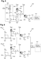
- FIG 3 schematically illustrates a synapse circuit 202 of the memory array of Figure 2 in more detail according to an example embodiment of the present disclosure.
- the synapse circuit 202 is for example suitable for performing variational inference. It would also be possible to use a similar synapse circuit for Markov chain Monte Carlo sampling, with the addition of an external memory for storing all of the samples that have been accepted by the algorithm.
- a relatively large number of samples is digitized, for example using an ADC applied to the varying voltage; and then a relatively large number of them are stored with an index that corresponds to "acceptance ratio" of that particular sample, the index being a number that can be calculated that estimates the posterior probability of that particular sample for the entire model given the data and the prior.
- the synapse circuit 202 for example comprises two resistive memory devices 302, 304 storing the two probability distribution parameters of the synapse.
- the device 302 is programmed to have a conductance G sigma representing a standard deviation of the desired probability distribution
- the device 304 is programmed to have a conductance G mu representing a mean of the desired probability distribution.
- the resistive memory devices 302, 304 are each for example resistive RAM (RRAM) devices.
- RRAM resistive RAM
- embodiments comprising oxide-based resistive RAM (OxRAM) devices are described, which are based on so-called “filamentary switching".
- PCM phase change memory
- RR_AM conductive bridge RR_AM
- ferromagnetic field effect transistors FLASH transistors, etc.
- Such devices are all capable of being programmed, in a non-volatile manner, to have a given conductance level.
- OxRAM devices have two electrodes separated by an oxide material, one example of which is hafnium dioxide.
- OxRAM devices are capable of being switched between high and low conductance states that respectively result from the absence or presence of a conductive oxygen vacancy filament within the oxide material.
- OxRAM devices can be SET to a high conductance state by applying a positive voltage across the device electrodes, the resulting conductance being proportional to the level of the current.
- OxR_AM devices can for example be RESET to the low conductive state by applying a negative voltage over the device electrodes, the resulting conductance being proportional to the magnitude of the RESET voltage.
- the resistive memory device 302 is coupled in series with a variable conductance 306 between the control line 206 and a reference voltage rail, which is for example a ground voltage rail.
- the variable conductance 306 for example has a conductance of G ref .
- the variable conductance 306 is implemented by a variable resistor, such as a polysilicon resistor, or by a pseudo transistor.
- the variable conductance 306 is controlled in order to conduct a biasing current i bias that is independent of the programmed conductance level of the resistive memory device 302.
- the variable conductance 306 is controlled by a current control circuit ( i bias CTRL) 307, for example implemented in the control circuit 212.
- the resistive memory device 302 is, for example, coupled in series with a selection transistor that can be used to select the device 302 during programming.
- the selection transistor could be an n-channel MOS (NMOS) transistor coupling the device 302 to the node 305, or coupling the node 305 to the conductance 306. It would also be possible for the selection transistor to form part of the circuit implementing the variable conductance 306.
- NMOS n-channel MOS
- the control circuit 212 of Figure 2 for example applies a voltage V read to the control line 206.
- a node 305 between the device 302 and the variable conductance 306 is for example coupled to one terminal of a capacitor 308, the other terminal of which is coupled to one terminal of the resistive memory device 304.
- the capacitor 308 for example provides a function of DC blocking.
- the capacitor 308 has a capacitance in the range 1 fF to 1 pF.
- the capacitor 308 is implemented by a MOSCAP.
- the resistive memory device 304 is for example coupled in series with a selection switch 310, implemented for example by an NMOS transistor, between the common neuron output line 204 and an output line 312 of the synapse circuit 202.
- the selection switch 310 is for example controlled via the control line 208 (see Figure 2 ).
- the control line 208 is coupled to the gate of the transistor implementing the switch 310.
- the source neuron (not illustrated in Figure 3 ) coupled to the synapse circuit 202 for example applies a data signal in the form of a voltage V data to the common neuron output line 204.
- the data signal V data is for example an analog voltage level generated by the source neuron.
- the data signal V data could be a binary voltage, if for example the cross-point is part of a spiking neural network.
- the control circuit 212 for example applies a voltage V gate to the control line 208.
- the output current i out of the synapse circuit 202 is for example provided, on the output line 312, which is also the input of the destination neuron.
- the output line 312 is coupled to the common neuron input line 210 providing the summed currents, from each synapse circuit of the row, to the destination neuron.
- the summed currents, including the output current i out of the synapse circuit 202, are for example sampled by an input circuit (NEURON SAMPLING) 314 of the destination neuron.
- variable conductance 306 and the application of the read voltage V read cause a current to be driven through the resistive memory device 302.
- Intrinsic Johnson-Nyquist noise also known as conductance fluctuations
- the resistive memory device 302 is for example programmed to be in the low conductance state, implying that it has a relatively high resistance, for example in the mega ohms or giga ohms range, and thus relatively high levels of Intrinsic Johnson-Nyquist noise.
- the device 302 is programmed to have a resistance of at least 100k ohms, and for example of at least 1M ohms.
- the voltage at the node 305 is thus a noisy Gaussian signal having a DC offset that depends on the values of G sigma and G ref .
- Figure 4A is a graph illustrating the voltage signal across a noisy resistive memory element 302 of the circuit of Figure 3 . It can be seen from the graph on the left of Figure 4 that the noise voltage density respects a Gaussian form. It can be seen from the graph on the right of Figure 4 that the noise signal has a mean ⁇ , an RMS (Root Mean Square) voltage level VnRMS corresponding to one standard deviation ⁇ from the mean, and a peak to peak level of 3.3 ⁇ .
- RMS Root Mean Square
- Figure 4B is a graph illustrating an example of the voltage V 1 at the node 305, corresponding to the Gaussian noise signal of Figure 4A , added to the DC offset V dc resulting from the voltage division between the device 302 and the variable conductance 306.
- the capacitor 308 removes the DC offset of the signal at node 305, and thus injects only the AC noisy Gaussian signal portion at the terminal of the resistive memory device 304.
- Figure 4C is a graph illustrating an example of the voltage signal V 2 at the node between capacitor 308 and the device 304, prior to the addition of the data encoding voltage V data .
- the resistive memory device 304 converts the sum of the voltages V data and V 2 into a current signal i out (t) in accordance with Ohms law.
- the device 304 is for example programmed to be in the high conductance state, and for example has a resistance of less than 20k ohms, and for example of less than 10k ohms.
- the resistance of the device 304 is significantly less than the resistance of the device 302, for example by at least two orders of magnitude, in other words the resistance of the device 304 being at least hundred times less than the resistance of the device 302.
- the amount of Intrinsic Johnson-Nyquist noise is relatively low, and can be ignored.
- This current i out (t) corresponds to a Gaussian distribution centered on G mu , with a standard deviation defined by the programmable noise of G sigma .
- This current i out (t) is for example sampled at the input of the destination neuron, as represented by the neuron sampling block 314 in Figure 3 .
- this may involve the use, in the destination neuron, of a resistor to convert the current into a voltage signal, and a sample and hold circuit to sample and store the voltage.
- a relatively short voltage pulse is applied as the gate signal V gate
- a relatively fast analog to digital converter in the neuron sampling circuit 314 is for example used to capture a digital value of the voltage measured during the voltage pulse.
- a relatively short voltage pulse is applied as the gate signal V gate , but the current is not converted into a voltage, but rather injected, for example via a current mirror, to a membrane capacitor of an analog neuron circuit.
- An example of an analog neuron circuit having such a membrane capacitor is described for example in the patent publication entitled "Neuromorphic Architecture" published as EP3855366A1 .
- capturing the instantaneous level of the current i out (t) is for example performed relatively quickly, such that the current/voltage fluctuations are not averaged over time.
- the duration of the sampling operation of the voltage V 2 is in the picosecond or nanosecond range, for example less than 10 nanoseconds, and in some cases in the range 1 picosecond to 5 nanoseconds.
- a calibration step is used to counteract a sampling time artefact and preserve a relatively large variation in the measured variance.
- the calibration step involves multiplying the value of ⁇ generated by the above equation by a constant between 1 and 0, for example to between 0.9 and 1.
- the capacitor 308 is configured to inject the AC noise signal at the input line 204 of the circuit
- the capacitor 308 could inject the AC noise signal at a different location.
- the capacitor 308 could be coupled between the node 305 and the node between the device 304 and the transistor 208, or even between the node 305 and the output line 210.
- the switch 310 could instead be coupled between the device 304 and the capacitor/line 204.
- Figure 5 schematically illustrates the synapse circuit 202 of the memory array of Figure 2 in more detail according to an alternative embodiment to that of Figure 3 .
- Certain features of the embodiment of Figure 5 are the same as those of the embodiment of Figure 3 , and these features are labelled with like reference numerals, and will not be described again in detail.
- the variable conductance 306 is implemented by a mirroring branch of a current mirror.
- the current mirror comprises a transistor 502 forming the mirroring branch, and a transistor 504 forming a reference branch.
- the transistor 502 is for example coupled by its main conducting nodes between the node 305 and a reference voltage rail, such as the ground rail.
- the transistor 504 is for example coupled by its main conducting nodes between a reference current input line 506 and the reference voltage rail.
- the transistors 502, 504 are for example MOS transistors having their gates coupled together and to the bias current input line 506.
- a reference current i ref of the current mirror is for example provided on the input line 506, for example by a current source 508.
- the current source 508 is selectively activated as a function of the voltage V read , such that the current in the current mirror is present only during a read operation.
- the current source 508 is variable, such that the reference current i ref can be adjusted based on the programmed resistance of the corresponding device 304.
- the current source 508 is capable of supplying one of a plurality of different current levels, for example at least four different current levels. This for example allows the magnitude of the noise voltage V 1 to be kept relatively close to a desired level, equal for example to around V read / 2.
- the control circuit 307 is for example configured to generate the control signal CTRL in order to control the current source 508 to supply an appropriate current.
- the current i bias is used to control the gate of the transistor 502 in order to provide a current through the resistive memory device 302 that is independent of the programmed conductance of the device 302.
- An advantage of the use of the current mirror in Figure 5 to generate the biasing current I bias is that temperature can be regulated by the current I ref .
- Figure 6 schematically illustrates a parallel arrangement 600 of a plurality M of the synapse circuits of Figure 5 , labelled 202_1 to 202_M.
- the parallel arrangement 600 corresponds to one row of synapse circuits 202 of the cross-point memory 200 of Figure 2 .
- the output lines 312 of the M synapse circuits are coupled together to form the common output line 210 of the row, which conducts a current SUM OUT, and is for example coupled to the sampling circuit (NEURON SAMPLING) 314 of the destination neuron.
- the reference current i ref provided to each reference branch 504 of the current mirror of each synapse circuit 202_1 to 202_M is for example a same current level.
- a common reference branch comprising the transistor 504
- the reference current i ref could be adjusted for each synapse circuit 202_1 to 202_M, as described above in relation with Figure 5 , based on the programmed resistance of the corresponding device 304, such that the magnitude of the noise voltage V 1 is kept relatively close to a desired level, equal for example to around V read / 2.
- Figure 7 schematically illustrates a synapse circuit 202 of the memory array of Figure 2 in more detail according to an alternative embodiment to those of Figures 3 and 5 , in which the synapse circuit 202 implements a Gaussian mixture synapse.
- This embodiment is based on Gaussian mixture model theory, which states that any arbitrary distribution can be approximated through a weighted sum of samples collected from a collection of Gaussian probability distributions. This principle is described in more detail in the publication by D. Reynolds entitled “Gaussian Mixture Models", Encyclopedia of biometrics 741 (2009): 659-663 .
- N synapse sub-circuits 700_1 to 700_N are arranged in parallel, each of these sub-circuits being implemented by a corresponding instantiation of the synapse circuit 202 of Figure 3 . It would alternatively be possible to implement the sub-circuits based on the synapse circuit 202 of Figure 5 .
- the output lines 312 of the sub-circuits 700_1 to 700_N are for example coupled together to form a single output line 312' of the synapse circuit 202.
- the synapse circuit 202 of Figure 7 further comprises, for example, a random number generator (RNG) 702 having its output coupled to a decoder circuit (DEC) 704, the decoder circuit 704 controlling the selection transistors 310 of the N sub-circuits 700_1 to 700_N.
- the decoder circuit 704 for example stores weighting factors (WEIGHTING FACTORS) 706 associated with each of the probability distributions of the sub-circuits 700_1 to 700_N. In some embodiments, all the weighting factors 706 sum to one.
- the decoder 704 is for example configured to provide a read signal to the transistor 310 of each sub-circuit 700_1 to 700_N depending on the value generated by the random number generator 702 and on the weighting factors 706.
- a dedicated random number generator 702 and decoder circuit 704 are for example provided for each synapse circuit 202 (i.e. each cross-point of Figure 2 ).
- the random number generator 702 it would however be possible to share the random number generator 702 by multiple synapse circuits 202, as in this case a random number can be generated only upon occurrence of spike, as described for example in the patent filing entitled "Neural network and method for variational inference" sharing the same priority date as the present filing and in the name of the same applicant (attorney reference B21181) .
- the random number generator 702 for example supplies a random value to the decoder circuit 704, which is for example configured to select one of the sub-circuits 700 1 to 700 N to be activated based on the random value.
- the random value is sampled from a uniform distribution.
- the range of possible values of the random value is for example divided into sub-ranges, each sub-range being associated with a corresponding one of the sub-circuits 700_1 to 700_N.
- the size of each sub-range represents the weighting factor of the corresponding sub-circuit, and is for example learned during variational inference.
- the decoder circuit 704 is for example configured to compare the random value with each of the sub-ranges, and to activate the sub-circuit 700_1 to 700_N that is associated with the sub-range within which the random value falls.
- the random value could be a 5-bit value having any value between 0 and 31.
- each sub-circuit is selected based on a new random value generated by the generator 702, and in this way each sub-circuit is selected a number of times that is proportional to its learned probability distribution weight, resulting in a Gaussian mixture, as represented in Figure 8 .
- Figure 8 is a graph illustrating probability density (PROBABILITY DENSITY) of a conductance (CONDUCTANCE, g ( ⁇ S)) of the synapse circuit 202 of Figure 7 according to an example embodiment of the present disclosure.
- Dashed-line curves K 1 to K 5 in Figure 8 represent examples of probability densities of five corresponding sub-circuits.
- a solid curve PD_mix illustrates an example of overall probability distribution that can be obtained by selecting a different one of the sub-circuits over many forward passes through the network.
- the resistive memory devices 302, 304 are respectively programmed based on learning during variational inference operations.
- the conductance G sigma of the device 302 is adjusted to an appropriate level to represent the standard deviation of the probability distribution
- the conductance G mu of the device 304 is adjusted to an appropriate level to represent the mean of the probability distribution.
- the amounts that the conductances of the devices should by adjusted during the learning phase are for example based on standard back propagation techniques, as described for example in the publication by Blundell, Charles, et al. entitled "Weight uncertainty in neural network" International Conference on Machine Learning. PMLR, 2015, and will not be described herein in detail. Examples of programming operations that can be used to program the conductances of the devices 302, 304 will now be described with reference to Figures 9 and 10 to 11.
- Figure 9 is a graph illustrating examples of conductance levels obtained by programming an OxRAM device during a SET operation into the high conductance/low resistance state.
- the graph of Figure 9 represents, for a SET programming current range 11 to 120 pA (CURRENT ( ⁇ A)), a median conductance (MEDIAN CONDUCTANCE ( ⁇ S )) represented by a curve 902 with a log scale on the left-hand axis, and a cycle-to-cycle standard deviation (CYCLE-TO-CYCLE S.D. %) of the conductance state following a RESET operation on the OxRAM device, represented by a curve 904 with a log scale on the right-hand axis. While the standard deviation is relatively high (around 70 %) for some lower conductances, the precision remains acceptable.
- Figure 10 schematically illustrates iterative programming of a resistive memory device according to an example embodiment.
- the example is based on the programming the devices 304 of the synapse circuits 202, for by programming a high conductance state (HCS) using a SET operation.
- HCS high conductance state
- Each device 304 is coupled in series with a programming selection transistor, which is for example the transistor 310 of Figure 3 , or another transistor.
- the programming selection transistors 310 are for example controlled by a voltage signal V gate , which is for example provided by the control circuit 212.
- V gate which is for example provided by the control circuit 212.
- the series connection of each device 302 and transistor 310 is coupled between a corresponding programming voltage line V[0], V[1] and V[2] and the output line 312, to which is applied a common bottom electrode voltage rail VBE.
- Each device 302 is for example programmed in turn, by applying, for example by the control circuit 212, a programming voltage to the corresponding voltage line V[0], V[1] and V[2], and asserting the voltage signal V gate in order to activate the corresponding conduction path through the device 304 to be programmed.
- a sufficiently precise target conductance of the device 304 is not always achieved after a single programming operation. It is therefore possible to apply an iterative programming approach.
- a read voltage is for example applied, by the control circuit 212, to the corresponding voltage line V[0], V[1] and V[2], and the resulting current on the line 312 is for example compared, by the control circuit 212, to a desired range in order to determine whether the conductance of the device has reached a desired conductance range, or whether it should be increased or decreased. If it is outside of the range, it is determined what adjustment should be applied to the programming voltage, and then the adjusted programming voltage is for example applied to the device in order to adjust its conductance level. In the case of a PCM device, the adjustment can be applied using a SET or RESET pulse to increase or decrease the conductance.
- a RESET operation is for example performed first, before then performing a new SET operation with a modified programming voltage.
- this process is for example repeated iteratively during several programming iterations (PROG. ITRN), until the conductance (CONDUCTANCE ( ⁇ S )) reaches a desired target range.
- the devices 302 of each synapse circuit 202 can for example be programmed using a similar technique to the one of Figure 10 .
- the devices 302 are for example programmed to the low conductance state (LCS) using a RESET operation.
- the transistors 310 other selection transistors are used, such as the transistors 502 of Figure 5 , and the rather than the common line 312, the selection transistors are coupled to another common line.
- This operation for example involves applying 0 V to the top electrode of the device 302 to be programmed, and applying a positive voltage to the common line, such that the device sees a negative voltage.
- An advantage of the embodiments described herein is that weights respecting given learned probability distributions can be sampled by synapse circuits in a simple and energy efficient manner.
- the currents used to generate the random distribution signals can be relatively low. For example, assuming a voltage V read of 0.4 V, which is for example chosen not to disturb the programmed state of the device 302, but to be high enough so as to saturate the current mirror transistors, that an LCS of 200 Mohms is used, and that the current mirror is also providing a resistance of about 200 Mohms, then by ohms law the current for generating the random distribution signal will be of around 1 nA. This compares to currents of tens or hundreds of microamps in the prior art solutions.
Landscapes
- Engineering & Computer Science (AREA)
- Physics & Mathematics (AREA)
- Theoretical Computer Science (AREA)
- General Physics & Mathematics (AREA)
- Life Sciences & Earth Sciences (AREA)
- Biomedical Technology (AREA)
- Biophysics (AREA)
- Health & Medical Sciences (AREA)
- Artificial Intelligence (AREA)
- Software Systems (AREA)
- Data Mining & Analysis (AREA)
- Evolutionary Computation (AREA)
- Mathematical Physics (AREA)
- Computing Systems (AREA)
- General Engineering & Computer Science (AREA)
- Molecular Biology (AREA)
- General Health & Medical Sciences (AREA)
- Computational Linguistics (AREA)
- Neurology (AREA)
- Probability & Statistics with Applications (AREA)
- Algebra (AREA)
- Computational Mathematics (AREA)
- Mathematical Analysis (AREA)
- Mathematical Optimization (AREA)
- Pure & Applied Mathematics (AREA)
- Semiconductor Memories (AREA)
Claims (13)
- Eine Synapsenschaltung (202) für ein Bayes'sches neuronales Netzwerk, wobei die Synapsenschaltung Folgendes aufweist:- eine erste resistive Speichervorrichtung (302), die eine erste Spannungsschiene (Vread, 206) mit einem ersten Anschluss eines Kondensators (308) koppelt, wobei der erste Anschluss des Kondensators (308) mit einer zweiten Spannungsschiene über eine variable Konduktivität (306) gekoppelt ist; und- eine zweite resistive Speichervorrichtung (304), die eine dritte Spannungsschiene (Vdata, 204) mit einer ersten Ausgansleitung (312) der Synapsenschaltung (202) koppelt, wobei ein zweiter Anschluss des Kondensators (306) mit einem Anschluss der zweiten resistiven Speichervorrichtung (304) gekoppelt ist.
- Die Synapsenschaltung nach Anspruch 1, ferner aufweisend einen Auswahlschalter (310), der in Serie mit der zweiten resistiven Speichervorrichtung (304) gekoppelt ist, so dass sie zusammen die dritte Spannungsschiene (Vdata, 204) mit der ersten Ausgangsleitung koppeln.
- Die Synapsenschaltung nach Anspruch 1 oder 2, wobei die variable Konduktivität (306) einen variablen Widerstand aufweist.
- Die Synapsenschaltung nach Anspruch 1 oder 2, wobei die variable Konduktivität (306) ein spiegelnder Zweig (502) eines Stromspiegels ist.
- Die Synapsenschaltung nach einem der Ansprüche 1 bis 4, ferner aufweisend eine Stromsteuerschaltung (307, 504, 508), die eingerichtet ist einen Vorspannungsstrom (ibias) zu regeln, den die variable Konduktivität (306) leitet.
- Die Synapsenschaltung nach einem der Ansprüche 1 bis 5, wobei die ersten und zweiten resistiven Speichervorrichtungen jeweils programmiert werden können, eines anzunehmen aus einem Zustand mit niedriger Leitfähigkeit, LCS (LCS = Low Conductance State), einem Zustand mit hoher Leitfähigkeit, HCS (HCS = High Conductance State), und wobei die erste resistive Speichervorrichtung (302) programmiert ist einen Zustand mit niedriger Leitfähigkeit, LCS, zu haben und die zweite resistive Speichervorrichtung (304) programmiert ist einen Zustand mit hoher Leitfähigkeit, HCS, zu haben.
- Die Synapsenschaltung nach einem der Ansprüche 1 bis 6, wobei die ersten und zweiten resistiven Speichervorrichtungen (302, 304) Oxid-basierte resistive Zufallszugriff-Speichervorrichtungen, OxRAM (OxRAM = Oxide-based Resistive Random Access Memory), sind.
- Die Synapsenschaltung nach Anspruch 2 oder einem der Ansprüche 3 bis 7, wenn sie von Anspruch 2 abhängen, wobei die Synapsenschaltung (202) eine Gauss'sche Mix-Synapse ist, wobei die erste und zweite resistive Speichervorrichtung (302, 304), der Kondensator (308), die variable Konduktivität (306) und ein Auswahlschalter (310) eine erste Unterschaltung (700_1) bilden, wobei die Synapsenschaltung ferner Folgendes aufweist:- wenigstens eine weitere Unterschaltung (700_N), die eine weitere resistive Speichervorrichtung (302) aufweist, die die erste Spannungsschiene (Vread ) mit einem ersten Anschluss eines weiteren Kondensators (308) koppelt, wobei der erste Anschluss des weiteren Kondensators (308) mit der zweiten Spannungsschiene über eine weitere variable Konduktivität (306) gekoppelt ist; eine zweite weitere resistive Speichervorrichtung (304) aufweist, die die dritte Spannungsschiene (Vdata ) mit einer Ausgangsleitung (312) der wenigstens einen weiteren Unterschaltung koppelt, wobei ein zweiter Anschluss des weiteren Kondensators (308) mit einem Anschluss der zweiten weiteren resistiven Speichervorrichtung (304) gekoppelt ist; und einen weiteren Auswahlschalter (310) aufweist, der in Serie mit der zweiten weiteren resistiven Speichervorrichtung (304) gekoppelt ist, so dass sie zusammen die dritte Spannungsschiene (Vdata, 204) mit der ersten Ausgangsleitung der wenigstens einen weiteren Unterschaltung koppeln, wobei die erste Ausgangsleitung (312) und die Ausgangsleitung der wenigstens einen weiteren Unterschaltung mit einer einzelnen Ausgangsleitung (312') der Gauss'schen Mix-Synapse gekoppelt sind; und- eine Auswahlschaltung (212), die eingerichtet ist, den Auswahlschalter (310) jeder Unterschaltung (700_1, 700_N) zu steuern.
- Die Synapsenschaltung nach Anspruch 8, wobei die Auswahlschaltung (212) einen Zufallszahl-Generator (702) aufweist, und eine Dekodier-Schaltung (704), die eingerichtet ist, den Auswahlschalter (310) jeder Unterschaltung (700_1, 700_N) zu steuern, und zwar basierend auf einem Zufallswert, der durch den Zufallszahl-Generator (702) erzeugt wurde.
- Eine Schnittpunkt-Speicher-Anordnung bzw. Speicher-Array zum Realisieren einer synaptischen Gewichtungs-Matrix zwischen Schichten eines neuronalen Netzwerks, wobei die Schnittpunkt-Speicher-Anordnung eine Vielzahl der Synapsenschaltungen (202) nach einem der Ansprüche 1 bis 8 aufweist, wobei jeweils eine an jedem Punkt der Schnittpunkt-Speicher-Anordnung positioniert ist.
- Ein Verfahren zum Erzeugen eines Stromsignals (iout(t)) auf einer Ausgangsleitung (312) einer Synapsenschaltung eines Bayes'schen neuronalen Netzwerks, wobei das Verfahren Folgendes aufweist:- Programmieren einer ersten resistiven Speichervorrichtung (302) der Synapsenschaltung (202), eine erste Leitfähigkeitsstufe (Gsigma) zu haben, wobei die erste resistive Speichervorrichtung (302) eine erste Spannungsschiene (Vread ) mit einem ersten Anschluss eines Kondensators (308) koppelt, wobei der erste Anschluss des Kondensators (308) mit einer zweiten Spannungsschiene über eine variable Konduktivität (306) gekoppelt ist;- Programmieren einer zweiten resistiven Speichervorrichtung (304) der Synapsenschaltung (202), eine zweite Leitfähigkeitsstufe (Gmu) zu haben, wobei die zweite resistive Speichervorrichtung (304) eine dritte Spannungsschiene (Vdata ) mit der ersten Ausgansleitung (312) der Synapsenschaltung (202) koppelt, wobei ein zweiter Anschluss des Kondensators (306) mit einem Anschluss der zweiten resistiven Speichervorrichtung (304) gekoppelt ist; und- Anlegen einer Spannung an die erste Spannungsschiene (Vread ) um ein Stromsignal (iout(t)) auf der Ausgangsleitung (312) zu erzeugen.
- Das Verfahren nach Anspruch 11, ferner aufweisend Abtasten des Stromsignals (iout(t)) um die momentane Stufe des Stromsignals (iout(t)) auf der Ausgangsleitung (312) zu erfassen.
- Das Verfahren nach Anspruch 11 oder 12, wobei die Synapsenschaltung ferner einen Auswahlschalter (310) aufweist, der in Serie mit der zweiten resistiven Speichervorrichtung (304) gekoppelt ist, so dass sie zusammen die dritte Spannungsschiene (Vdata ) mit der ersten Ausgangsleitung (312) koppeln, wobei das Verfahren ferner Aktivieren des Auswahlschalters (310) aufweist, und zwar während dem Anlegen der Spannung an die erste Spannungsschiene (Vread ) um das Stromsignal (iout(t)) auf der Ausgangsleitung (312) zu erzeugen.
Priority Applications (3)
| Application Number | Priority Date | Filing Date | Title |
|---|---|---|---|
| EP21306485.0A EP4174724B1 (de) | 2021-10-26 | 2021-10-26 | Synapsenschaltung für variationale inferenz |
| US18/046,926 US20230125074A1 (en) | 2021-10-26 | 2022-10-16 | Synapse circuit for variational inference |
| JP2022169949A JP2023064732A (ja) | 2021-10-26 | 2022-10-24 | 変分推論のためのシナプス回路 |
Applications Claiming Priority (1)
| Application Number | Priority Date | Filing Date | Title |
|---|---|---|---|
| EP21306485.0A EP4174724B1 (de) | 2021-10-26 | 2021-10-26 | Synapsenschaltung für variationale inferenz |
Publications (2)
| Publication Number | Publication Date |
|---|---|
| EP4174724A1 EP4174724A1 (de) | 2023-05-03 |
| EP4174724B1 true EP4174724B1 (de) | 2023-10-11 |
Family
ID=78592775
Family Applications (1)
| Application Number | Title | Priority Date | Filing Date |
|---|---|---|---|
| EP21306485.0A Active EP4174724B1 (de) | 2021-10-26 | 2021-10-26 | Synapsenschaltung für variationale inferenz |
Country Status (3)
| Country | Link |
|---|---|
| US (1) | US20230125074A1 (de) |
| EP (1) | EP4174724B1 (de) |
| JP (1) | JP2023064732A (de) |
Cited By (1)
| Publication number | Priority date | Publication date | Assignee | Title |
|---|---|---|---|---|
| EP4749625A1 (de) | 2024-11-26 | 2026-05-27 | Commissariat à l'Energie Atomique et aux Energies Alternatives | Elektronische schaltung zur implementierung eines bayesschen neuronalen netzwerks |
Families Citing this family (4)
| Publication number | Priority date | Publication date | Assignee | Title |
|---|---|---|---|---|
| KR20230027453A (ko) * | 2021-08-19 | 2023-02-28 | 삼성전자주식회사 | 저항성 소자를 사용하는 용량성 커플링 기반 인메모리 컴퓨팅 장치 및 방법 |
| EP4357980A1 (de) * | 2022-10-21 | 2024-04-24 | Commissariat à l'énergie atomique et aux énergies alternatives | Neuronale netzwerkschaltung mit verzögerungsleitung |
| FR3153915B1 (fr) * | 2023-10-05 | 2026-06-26 | Commissariat Energie Atomique | Génération de valeurs aléatoires physiques à l'aide d'un dispositif de mémoire résistive |
| US20250140315A1 (en) * | 2023-10-25 | 2025-05-01 | Anaflash Inc. | Floating Metal Based Flash Memory |
Family Cites Families (1)
| Publication number | Priority date | Publication date | Assignee | Title |
|---|---|---|---|---|
| FR3106681B1 (fr) | 2020-01-24 | 2022-05-06 | Commissariat Energie Atomique | Architecture neuromorphique |
-
2021
- 2021-10-26 EP EP21306485.0A patent/EP4174724B1/de active Active
-
2022
- 2022-10-16 US US18/046,926 patent/US20230125074A1/en active Pending
- 2022-10-24 JP JP2022169949A patent/JP2023064732A/ja active Pending
Cited By (2)
| Publication number | Priority date | Publication date | Assignee | Title |
|---|---|---|---|---|
| EP4749625A1 (de) | 2024-11-26 | 2026-05-27 | Commissariat à l'Energie Atomique et aux Energies Alternatives | Elektronische schaltung zur implementierung eines bayesschen neuronalen netzwerks |
| FR3169000A1 (fr) | 2024-11-26 | 2026-05-29 | Commissariat à l'Energie Atomique et aux Energies Alternatives | Circuit électronique pour la mise en œuvre d’un réseau neuronal bayésien |
Also Published As
| Publication number | Publication date |
|---|---|
| US20230125074A1 (en) | 2023-04-27 |
| EP4174724A1 (de) | 2023-05-03 |
| JP2023064732A (ja) | 2023-05-11 |
Similar Documents
| Publication | Publication Date | Title |
|---|---|---|
| US20230125074A1 (en) | Synapse circuit for variational inference | |
| Wijesinghe et al. | An all-memristor deep spiking neural computing system: A step toward realizing the low-power stochastic brain | |
| Boybat et al. | Neuromorphic computing with multi-memristive synapses | |
| US8447714B2 (en) | System for electronic learning synapse with spike-timing dependent plasticity using phase change memory | |
| US10810489B2 (en) | Neuron peripheral circuits for neuromorphic synaptic memory array based on neuron models | |
| US20190122105A1 (en) | Training of artificial neural networks | |
| US10902317B2 (en) | Neural network processing system | |
| US11347999B2 (en) | Closed loop programming of phase-change memory | |
| US10217046B2 (en) | Neuromorphic processing devices | |
| US8250010B2 (en) | Electronic learning synapse with spike-timing dependent plasticity using unipolar memory-switching elements | |
| Pedretti et al. | Conductance variations and their impact on the precision of in-memory computing with resistive switching memory (RRAM) | |
| Prezioso et al. | Modeling and implementation of firing-rate neuromorphic-network classifiers with bilayer Pt/Al2O3/TiO2− x/Pt memristors | |
| JP2021507349A (ja) | 抵抗処理ユニット・アレイのクロスポイント・デバイスに重みを記憶するための方法、そのクロスポイント・デバイス、ニューラル・ネットワークを実施するためのクロスポイント・アレイ、そのシステム、およびニューラル・ネットワークを実施するための方法 | |
| Antolini et al. | Combined HW/SW drift and variability mitigation for PCM-based analog in-memory computing for neural network applications | |
| WO2018158680A1 (en) | Resistive processing unit with hysteretic updates for neural network training | |
| Lin et al. | Analysis and simulation of capacitor-less ReRAM-based stochastic neurons for the in-memory spiking neural network | |
| Ahmadi-Farsani et al. | A CMOS–memristor hybrid system for implementing stochastic binary spike timing-dependent plasticity | |
| Suri et al. | Addition of HfO2 interface layer for improved synaptic performance of phase change memory (PCM) devices | |
| Dalgaty et al. | Hybrid CMOS-RRAM neurons with intrinsic plasticity | |
| Bertuletti et al. | A multilayer neural accelerator with binary activations based on phase-change memory | |
| Afshari et al. | Analyzing the impact of memristor variability on crossbar implementation of regression algorithms with smart weight update pulsing techniques | |
| Johari et al. | CMOS-memristor hybrid design of a neuromorphic crossbar array with integrated inference and training | |
| Byun et al. | Reset-dominant accurate synaptic weight mapping in passive memristor arrays for energy-efficient spiking neural networks | |
| Ghongade et al. | Spiking neural network architectures with memristive synapses for energy-efficient edge intelligence: A hardware-software co-design framework | |
| EP4095759A1 (de) | Verfahren zum trainieren eines binarisierten neuronalen netzes und zugehörige elektronische schaltung |
Legal Events
| Date | Code | Title | Description |
|---|---|---|---|
| PUAI | Public reference made under article 153(3) epc to a published international application that has entered the european phase |
Free format text: ORIGINAL CODE: 0009012 |
|
| STAA | Information on the status of an ep patent application or granted ep patent |
Free format text: STATUS: THE APPLICATION HAS BEEN PUBLISHED |
|
| AK | Designated contracting states |
Kind code of ref document: A1 Designated state(s): AL AT BE BG CH CY CZ DE DK EE ES FI FR GB GR HR HU IE IS IT LI LT LU LV MC MK MT NL NO PL PT RO RS SE SI SK SM TR |
|
| STAA | Information on the status of an ep patent application or granted ep patent |
Free format text: STATUS: REQUEST FOR EXAMINATION WAS MADE |
|
| 17P | Request for examination filed |
Effective date: 20230515 |
|
| RBV | Designated contracting states (corrected) |
Designated state(s): AL AT BE BG CH CY CZ DE DK EE ES FI FR GB GR HR HU IE IS IT LI LT LU LV MC MK MT NL NO PL PT RO RS SE SI SK SM TR |
|
| REG | Reference to a national code |
Ref legal event code: R079 Ipc: G06N0003065000 Ref country code: DE Ref legal event code: R079 Ref document number: 602021005822 Country of ref document: DE Free format text: PREVIOUS MAIN CLASS: G06N0003063000 Ipc: G06N0003065000 |
|
| GRAP | Despatch of communication of intention to grant a patent |
Free format text: ORIGINAL CODE: EPIDOSNIGR1 |
|
| STAA | Information on the status of an ep patent application or granted ep patent |
Free format text: STATUS: GRANT OF PATENT IS INTENDED |
|
| RIC1 | Information provided on ipc code assigned before grant |
Ipc: G06N 3/084 20230101ALN20230622BHEP Ipc: G06N 3/047 20230101ALI20230622BHEP Ipc: G06N 3/065 20230101AFI20230622BHEP |
|
| RIC1 | Information provided on ipc code assigned before grant |
Ipc: G06N 3/084 20230101ALN20230703BHEP Ipc: G06N 3/047 20230101ALI20230703BHEP Ipc: G06N 3/065 20230101AFI20230703BHEP |
|
| INTG | Intention to grant announced |
Effective date: 20230718 |
|
| GRAS | Grant fee paid |
Free format text: ORIGINAL CODE: EPIDOSNIGR3 |
|
| GRAA | (expected) grant |
Free format text: ORIGINAL CODE: 0009210 |
|
| STAA | Information on the status of an ep patent application or granted ep patent |
Free format text: STATUS: THE PATENT HAS BEEN GRANTED |
|
| AK | Designated contracting states |
Kind code of ref document: B1 Designated state(s): AL AT BE BG CH CY CZ DE DK EE ES FI FR GB GR HR HU IE IS IT LI LT LU LV MC MK MT NL NO PL PT RO RS SE SI SK SM TR |
|
| REG | Reference to a national code |
Ref country code: GB Ref legal event code: FG4D |
|
| REG | Reference to a national code |
Ref country code: CH Ref legal event code: EP |
|
| REG | Reference to a national code |
Ref country code: DE Ref legal event code: R096 Ref document number: 602021005822 Country of ref document: DE |
|
| REG | Reference to a national code |
Ref country code: IE Ref legal event code: FG4D |
|
| REG | Reference to a national code |
Ref country code: LT Ref legal event code: MG9D |
|
| REG | Reference to a national code |
Ref country code: NL Ref legal event code: MP Effective date: 20231011 |
|
| REG | Reference to a national code |
Ref country code: AT Ref legal event code: MK05 Ref document number: 1620950 Country of ref document: AT Kind code of ref document: T Effective date: 20231011 |
|
| PG25 | Lapsed in a contracting state [announced via postgrant information from national office to epo] |
Ref country code: NL Free format text: LAPSE BECAUSE OF FAILURE TO SUBMIT A TRANSLATION OF THE DESCRIPTION OR TO PAY THE FEE WITHIN THE PRESCRIBED TIME-LIMIT Effective date: 20231011 |
|
| PG25 | Lapsed in a contracting state [announced via postgrant information from national office to epo] |
Ref country code: GR Free format text: LAPSE BECAUSE OF FAILURE TO SUBMIT A TRANSLATION OF THE DESCRIPTION OR TO PAY THE FEE WITHIN THE PRESCRIBED TIME-LIMIT Effective date: 20240112 |
|
| PG25 | Lapsed in a contracting state [announced via postgrant information from national office to epo] |
Ref country code: IS Free format text: LAPSE BECAUSE OF FAILURE TO SUBMIT A TRANSLATION OF THE DESCRIPTION OR TO PAY THE FEE WITHIN THE PRESCRIBED TIME-LIMIT Effective date: 20240211 |
|
| PG25 | Lapsed in a contracting state [announced via postgrant information from national office to epo] |
Ref country code: LT Free format text: LAPSE BECAUSE OF FAILURE TO SUBMIT A TRANSLATION OF THE DESCRIPTION OR TO PAY THE FEE WITHIN THE PRESCRIBED TIME-LIMIT Effective date: 20231011 |
|
| PG25 | Lapsed in a contracting state [announced via postgrant information from national office to epo] |
Ref country code: AT Free format text: LAPSE BECAUSE OF FAILURE TO SUBMIT A TRANSLATION OF THE DESCRIPTION OR TO PAY THE FEE WITHIN THE PRESCRIBED TIME-LIMIT Effective date: 20231011 |
|
| PG25 | Lapsed in a contracting state [announced via postgrant information from national office to epo] |
Ref country code: ES Free format text: LAPSE BECAUSE OF FAILURE TO SUBMIT A TRANSLATION OF THE DESCRIPTION OR TO PAY THE FEE WITHIN THE PRESCRIBED TIME-LIMIT Effective date: 20231011 |
|
| PG25 | Lapsed in a contracting state [announced via postgrant information from national office to epo] |
Ref country code: LT Free format text: LAPSE BECAUSE OF FAILURE TO SUBMIT A TRANSLATION OF THE DESCRIPTION OR TO PAY THE FEE WITHIN THE PRESCRIBED TIME-LIMIT Effective date: 20231011 Ref country code: IS Free format text: LAPSE BECAUSE OF FAILURE TO SUBMIT A TRANSLATION OF THE DESCRIPTION OR TO PAY THE FEE WITHIN THE PRESCRIBED TIME-LIMIT Effective date: 20240211 Ref country code: GR Free format text: LAPSE BECAUSE OF FAILURE TO SUBMIT A TRANSLATION OF THE DESCRIPTION OR TO PAY THE FEE WITHIN THE PRESCRIBED TIME-LIMIT Effective date: 20240112 Ref country code: ES Free format text: LAPSE BECAUSE OF FAILURE TO SUBMIT A TRANSLATION OF THE DESCRIPTION OR TO PAY THE FEE WITHIN THE PRESCRIBED TIME-LIMIT Effective date: 20231011 Ref country code: BG Free format text: LAPSE BECAUSE OF FAILURE TO SUBMIT A TRANSLATION OF THE DESCRIPTION OR TO PAY THE FEE WITHIN THE PRESCRIBED TIME-LIMIT Effective date: 20240111 Ref country code: AT Free format text: LAPSE BECAUSE OF FAILURE TO SUBMIT A TRANSLATION OF THE DESCRIPTION OR TO PAY THE FEE WITHIN THE PRESCRIBED TIME-LIMIT Effective date: 20231011 Ref country code: PT Free format text: LAPSE BECAUSE OF FAILURE TO SUBMIT A TRANSLATION OF THE DESCRIPTION OR TO PAY THE FEE WITHIN THE PRESCRIBED TIME-LIMIT Effective date: 20240212 |
|
| PG25 | Lapsed in a contracting state [announced via postgrant information from national office to epo] |
Ref country code: SE Free format text: LAPSE BECAUSE OF FAILURE TO SUBMIT A TRANSLATION OF THE DESCRIPTION OR TO PAY THE FEE WITHIN THE PRESCRIBED TIME-LIMIT Effective date: 20231011 Ref country code: RS Free format text: LAPSE BECAUSE OF FAILURE TO SUBMIT A TRANSLATION OF THE DESCRIPTION OR TO PAY THE FEE WITHIN THE PRESCRIBED TIME-LIMIT Effective date: 20231011 Ref country code: PL Free format text: LAPSE BECAUSE OF FAILURE TO SUBMIT A TRANSLATION OF THE DESCRIPTION OR TO PAY THE FEE WITHIN THE PRESCRIBED TIME-LIMIT Effective date: 20231011 Ref country code: NO Free format text: LAPSE BECAUSE OF FAILURE TO SUBMIT A TRANSLATION OF THE DESCRIPTION OR TO PAY THE FEE WITHIN THE PRESCRIBED TIME-LIMIT Effective date: 20240111 Ref country code: LV Free format text: LAPSE BECAUSE OF FAILURE TO SUBMIT A TRANSLATION OF THE DESCRIPTION OR TO PAY THE FEE WITHIN THE PRESCRIBED TIME-LIMIT Effective date: 20231011 Ref country code: HR Free format text: LAPSE BECAUSE OF FAILURE TO SUBMIT A TRANSLATION OF THE DESCRIPTION OR TO PAY THE FEE WITHIN THE PRESCRIBED TIME-LIMIT Effective date: 20231011 |
|
| REG | Reference to a national code |
Ref country code: BE Ref legal event code: MM Effective date: 20231031 |
|
| PG25 | Lapsed in a contracting state [announced via postgrant information from national office to epo] |
Ref country code: LU Free format text: LAPSE BECAUSE OF NON-PAYMENT OF DUE FEES Effective date: 20231026 |
|
| PG25 | Lapsed in a contracting state [announced via postgrant information from national office to epo] |
Ref country code: LU Free format text: LAPSE BECAUSE OF NON-PAYMENT OF DUE FEES Effective date: 20231026 |
|
| PG25 | Lapsed in a contracting state [announced via postgrant information from national office to epo] |
Ref country code: DK Free format text: LAPSE BECAUSE OF FAILURE TO SUBMIT A TRANSLATION OF THE DESCRIPTION OR TO PAY THE FEE WITHIN THE PRESCRIBED TIME-LIMIT Effective date: 20231011 |
|
| REG | Reference to a national code |
Ref country code: DE Ref legal event code: R097 Ref document number: 602021005822 Country of ref document: DE |
|
| PG25 | Lapsed in a contracting state [announced via postgrant information from national office to epo] |
Ref country code: CZ Free format text: LAPSE BECAUSE OF FAILURE TO SUBMIT A TRANSLATION OF THE DESCRIPTION OR TO PAY THE FEE WITHIN THE PRESCRIBED TIME-LIMIT Effective date: 20231011 |
|
| PG25 | Lapsed in a contracting state [announced via postgrant information from national office to epo] |
Ref country code: SK Free format text: LAPSE BECAUSE OF FAILURE TO SUBMIT A TRANSLATION OF THE DESCRIPTION OR TO PAY THE FEE WITHIN THE PRESCRIBED TIME-LIMIT Effective date: 20231011 |
|
| PG25 | Lapsed in a contracting state [announced via postgrant information from national office to epo] |
Ref country code: SM Free format text: LAPSE BECAUSE OF FAILURE TO SUBMIT A TRANSLATION OF THE DESCRIPTION OR TO PAY THE FEE WITHIN THE PRESCRIBED TIME-LIMIT Effective date: 20231011 Ref country code: SK Free format text: LAPSE BECAUSE OF FAILURE TO SUBMIT A TRANSLATION OF THE DESCRIPTION OR TO PAY THE FEE WITHIN THE PRESCRIBED TIME-LIMIT Effective date: 20231011 Ref country code: RO Free format text: LAPSE BECAUSE OF FAILURE TO SUBMIT A TRANSLATION OF THE DESCRIPTION OR TO PAY THE FEE WITHIN THE PRESCRIBED TIME-LIMIT Effective date: 20231011 Ref country code: IT Free format text: LAPSE BECAUSE OF FAILURE TO SUBMIT A TRANSLATION OF THE DESCRIPTION OR TO PAY THE FEE WITHIN THE PRESCRIBED TIME-LIMIT Effective date: 20231011 Ref country code: EE Free format text: LAPSE BECAUSE OF FAILURE TO SUBMIT A TRANSLATION OF THE DESCRIPTION OR TO PAY THE FEE WITHIN THE PRESCRIBED TIME-LIMIT Effective date: 20231011 Ref country code: DK Free format text: LAPSE BECAUSE OF FAILURE TO SUBMIT A TRANSLATION OF THE DESCRIPTION OR TO PAY THE FEE WITHIN THE PRESCRIBED TIME-LIMIT Effective date: 20231011 Ref country code: CZ Free format text: LAPSE BECAUSE OF FAILURE TO SUBMIT A TRANSLATION OF THE DESCRIPTION OR TO PAY THE FEE WITHIN THE PRESCRIBED TIME-LIMIT Effective date: 20231011 |
|
| PLBE | No opposition filed within time limit |
Free format text: ORIGINAL CODE: 0009261 |
|
| STAA | Information on the status of an ep patent application or granted ep patent |
Free format text: STATUS: NO OPPOSITION FILED WITHIN TIME LIMIT |
|
| PG25 | Lapsed in a contracting state [announced via postgrant information from national office to epo] |
Ref country code: MC Free format text: LAPSE BECAUSE OF FAILURE TO SUBMIT A TRANSLATION OF THE DESCRIPTION OR TO PAY THE FEE WITHIN THE PRESCRIBED TIME-LIMIT Effective date: 20231011 |
|
| PG25 | Lapsed in a contracting state [announced via postgrant information from national office to epo] |
Ref country code: MC Free format text: LAPSE BECAUSE OF FAILURE TO SUBMIT A TRANSLATION OF THE DESCRIPTION OR TO PAY THE FEE WITHIN THE PRESCRIBED TIME-LIMIT Effective date: 20231011 Ref country code: BE Free format text: LAPSE BECAUSE OF NON-PAYMENT OF DUE FEES Effective date: 20231031 |
|
| 26N | No opposition filed |
Effective date: 20240712 |
|
| PG25 | Lapsed in a contracting state [announced via postgrant information from national office to epo] |
Ref country code: IE Free format text: LAPSE BECAUSE OF NON-PAYMENT OF DUE FEES Effective date: 20231026 |
|
| PG25 | Lapsed in a contracting state [announced via postgrant information from national office to epo] |
Ref country code: SI Free format text: LAPSE BECAUSE OF FAILURE TO SUBMIT A TRANSLATION OF THE DESCRIPTION OR TO PAY THE FEE WITHIN THE PRESCRIBED TIME-LIMIT Effective date: 20231011 |
|
| PG25 | Lapsed in a contracting state [announced via postgrant information from national office to epo] |
Ref country code: SI Free format text: LAPSE BECAUSE OF FAILURE TO SUBMIT A TRANSLATION OF THE DESCRIPTION OR TO PAY THE FEE WITHIN THE PRESCRIBED TIME-LIMIT Effective date: 20231011 Ref country code: IE Free format text: LAPSE BECAUSE OF NON-PAYMENT OF DUE FEES Effective date: 20231026 |
|
| REG | Reference to a national code |
Ref country code: CH Ref legal event code: PL |
|
| PG25 | Lapsed in a contracting state [announced via postgrant information from national office to epo] |
Ref country code: FI Free format text: LAPSE BECAUSE OF FAILURE TO SUBMIT A TRANSLATION OF THE DESCRIPTION OR TO PAY THE FEE WITHIN THE PRESCRIBED TIME-LIMIT Effective date: 20231011 |
|
| PG25 | Lapsed in a contracting state [announced via postgrant information from national office to epo] |
Ref country code: CH Free format text: LAPSE BECAUSE OF NON-PAYMENT OF DUE FEES Effective date: 20241031 |
|
| PG25 | Lapsed in a contracting state [announced via postgrant information from national office to epo] |
Ref country code: CY Free format text: LAPSE BECAUSE OF FAILURE TO SUBMIT A TRANSLATION OF THE DESCRIPTION OR TO PAY THE FEE WITHIN THE PRESCRIBED TIME-LIMIT; INVALID AB INITIO Effective date: 20211026 |
|
| PG25 | Lapsed in a contracting state [announced via postgrant information from national office to epo] |
Ref country code: TR Free format text: LAPSE BECAUSE OF FAILURE TO SUBMIT A TRANSLATION OF THE DESCRIPTION OR TO PAY THE FEE WITHIN THE PRESCRIBED TIME-LIMIT Effective date: 20231011 |
|
| PGFP | Annual fee paid to national office [announced via postgrant information from national office to epo] |
Ref country code: DE Payment date: 20251020 Year of fee payment: 5 |
|
| PGFP | Annual fee paid to national office [announced via postgrant information from national office to epo] |
Ref country code: FR Payment date: 20251023 Year of fee payment: 5 |
|
| PG25 | Lapsed in a contracting state [announced via postgrant information from national office to epo] |
Ref country code: HU Free format text: LAPSE BECAUSE OF FAILURE TO SUBMIT A TRANSLATION OF THE DESCRIPTION OR TO PAY THE FEE WITHIN THE PRESCRIBED TIME-LIMIT; INVALID AB INITIO Effective date: 20211026 |
|
| PG25 | Lapsed in a contracting state [announced via postgrant information from national office to epo] |
Ref country code: CH Free format text: THE PATENT HAS BEEN ANNULLED BY A DECISION OF A NATIONAL AUTHORITY Effective date: 20241031 |
|
| GBPC | Gb: european patent ceased through non-payment of renewal fee |
Effective date: 20251026 |
|
| PG25 | Lapsed in a contracting state [announced via postgrant information from national office to epo] |
Ref country code: GB Free format text: LAPSE BECAUSE OF NON-PAYMENT OF DUE FEES Effective date: 20251026 |