EP4174666B1 - Speicherverwaltungstechnologie und computersystem - Google Patents
Speicherverwaltungstechnologie und computersystem Download PDFInfo
- Publication number
- EP4174666B1 EP4174666B1 EP21842284.8A EP21842284A EP4174666B1 EP 4174666 B1 EP4174666 B1 EP 4174666B1 EP 21842284 A EP21842284 A EP 21842284A EP 4174666 B1 EP4174666 B1 EP 4174666B1
- Authority
- EP
- European Patent Office
- Prior art keywords
- row
- memory
- access
- target
- indicator
- Prior art date
- Legal status (The legal status is an assumption and is not a legal conclusion. Google has not performed a legal analysis and makes no representation as to the accuracy of the status listed.)
- Active
Links
Images


Classifications
-
- G—PHYSICS
- G11—INFORMATION STORAGE
- G11C—STATIC STORES
- G11C11/00—Digital stores characterised by the use of particular electric or magnetic storage elements; Storage elements therefor
- G11C11/21—Digital stores characterised by the use of particular electric or magnetic storage elements; Storage elements therefor using electric elements
- G11C11/34—Digital stores characterised by the use of particular electric or magnetic storage elements; Storage elements therefor using electric elements using semiconductor devices
- G11C11/40—Digital stores characterised by the use of particular electric or magnetic storage elements; Storage elements therefor using electric elements using semiconductor devices using transistors
- G11C11/401—Digital stores characterised by the use of particular electric or magnetic storage elements; Storage elements therefor using electric elements using semiconductor devices using transistors forming cells needing refreshing or charge regeneration, i.e. dynamic cells
- G11C11/4063—Auxiliary circuits, e.g. for addressing, decoding, driving, writing, sensing or timing
- G11C11/407—Auxiliary circuits, e.g. for addressing, decoding, driving, writing, sensing or timing for memory cells of the field-effect type
- G11C11/4076—Timing circuits
-
- G—PHYSICS
- G06—COMPUTING OR CALCULATING; COUNTING
- G06F—ELECTRIC DIGITAL DATA PROCESSING
- G06F3/00—Input arrangements for transferring data to be processed into a form capable of being handled by the computer; Output arrangements for transferring data from processing unit to output unit, e.g. interface arrangements
- G06F3/06—Digital input from, or digital output to, record carriers, e.g. RAID, emulated record carriers or networked record carriers
- G06F3/0601—Interfaces specially adapted for storage systems
- G06F3/0602—Interfaces specially adapted for storage systems specifically adapted to achieve a particular effect
- G06F3/061—Improving I/O performance
- G06F3/0611—Improving I/O performance in relation to response time
-
- G—PHYSICS
- G06—COMPUTING OR CALCULATING; COUNTING
- G06F—ELECTRIC DIGITAL DATA PROCESSING
- G06F12/00—Accessing, addressing or allocating within memory systems or architectures
- G06F12/02—Addressing or allocation; Relocation
- G06F12/0215—Addressing or allocation; Relocation with look ahead addressing means
-
- G—PHYSICS
- G06—COMPUTING OR CALCULATING; COUNTING
- G06F—ELECTRIC DIGITAL DATA PROCESSING
- G06F13/00—Interconnection of, or transfer of information or other signals between, memories, input/output devices or central processing units
- G06F13/14—Handling requests for interconnection or transfer
- G06F13/16—Handling requests for interconnection or transfer for access to memory bus
- G06F13/1605—Handling requests for interconnection or transfer for access to memory bus based on arbitration
- G06F13/161—Handling requests for interconnection or transfer for access to memory bus based on arbitration with latency improvement
-
- G—PHYSICS
- G06—COMPUTING OR CALCULATING; COUNTING
- G06F—ELECTRIC DIGITAL DATA PROCESSING
- G06F3/00—Input arrangements for transferring data to be processed into a form capable of being handled by the computer; Output arrangements for transferring data from processing unit to output unit, e.g. interface arrangements
- G06F3/06—Digital input from, or digital output to, record carriers, e.g. RAID, emulated record carriers or networked record carriers
- G06F3/0601—Interfaces specially adapted for storage systems
- G06F3/0628—Interfaces specially adapted for storage systems making use of a particular technique
- G06F3/0653—Monitoring storage devices or systems
-
- G—PHYSICS
- G06—COMPUTING OR CALCULATING; COUNTING
- G06F—ELECTRIC DIGITAL DATA PROCESSING
- G06F3/00—Input arrangements for transferring data to be processed into a form capable of being handled by the computer; Output arrangements for transferring data from processing unit to output unit, e.g. interface arrangements
- G06F3/06—Digital input from, or digital output to, record carriers, e.g. RAID, emulated record carriers or networked record carriers
- G06F3/0601—Interfaces specially adapted for storage systems
- G06F3/0628—Interfaces specially adapted for storage systems making use of a particular technique
- G06F3/0655—Vertical data movement, i.e. input-output transfer; data movement between one or more hosts and one or more storage devices
- G06F3/0659—Command handling arrangements, e.g. command buffers, queues, command scheduling
-
- G—PHYSICS
- G06—COMPUTING OR CALCULATING; COUNTING
- G06F—ELECTRIC DIGITAL DATA PROCESSING
- G06F3/00—Input arrangements for transferring data to be processed into a form capable of being handled by the computer; Output arrangements for transferring data from processing unit to output unit, e.g. interface arrangements
- G06F3/06—Digital input from, or digital output to, record carriers, e.g. RAID, emulated record carriers or networked record carriers
- G06F3/0601—Interfaces specially adapted for storage systems
- G06F3/0668—Interfaces specially adapted for storage systems adopting a particular infrastructure
- G06F3/0671—In-line storage system
- G06F3/0673—Single storage device
-
- G—PHYSICS
- G06—COMPUTING OR CALCULATING; COUNTING
- G06F—ELECTRIC DIGITAL DATA PROCESSING
- G06F9/00—Arrangements for program control, e.g. control units
- G06F9/06—Arrangements for program control, e.g. control units using stored programs, i.e. using an internal store of processing equipment to receive or retain programs
- G06F9/46—Multiprogramming arrangements
- G06F9/50—Allocation of resources, e.g. of the central processing unit [CPU]
- G06F9/5005—Allocation of resources, e.g. of the central processing unit [CPU] to service a request
- G06F9/5011—Allocation of resources, e.g. of the central processing unit [CPU] to service a request the resources being hardware resources other than CPUs, Servers and Terminals
- G06F9/5016—Allocation of resources, e.g. of the central processing unit [CPU] to service a request the resources being hardware resources other than CPUs, Servers and Terminals the resource being the memory
-
- G—PHYSICS
- G11—INFORMATION STORAGE
- G11C—STATIC STORES
- G11C11/00—Digital stores characterised by the use of particular electric or magnetic storage elements; Storage elements therefor
- G11C11/21—Digital stores characterised by the use of particular electric or magnetic storage elements; Storage elements therefor using electric elements
- G11C11/34—Digital stores characterised by the use of particular electric or magnetic storage elements; Storage elements therefor using electric elements using semiconductor devices
- G11C11/40—Digital stores characterised by the use of particular electric or magnetic storage elements; Storage elements therefor using electric elements using semiconductor devices using transistors
- G11C11/401—Digital stores characterised by the use of particular electric or magnetic storage elements; Storage elements therefor using electric elements using semiconductor devices using transistors forming cells needing refreshing or charge regeneration, i.e. dynamic cells
- G11C11/4063—Auxiliary circuits, e.g. for addressing, decoding, driving, writing, sensing or timing
-
- G—PHYSICS
- G11—INFORMATION STORAGE
- G11C—STATIC STORES
- G11C7/00—Arrangements for writing information into, or reading information out from, a digital store
- G11C7/22—Read-write [R-W] timing or clocking circuits; Read-write [R-W] control signal generators or management
-
- G—PHYSICS
- G06—COMPUTING OR CALCULATING; COUNTING
- G06F—ELECTRIC DIGITAL DATA PROCESSING
- G06F2212/00—Indexing scheme relating to accessing, addressing or allocation within memory systems or architectures
- G06F2212/10—Providing a specific technical effect
- G06F2212/1016—Performance improvement
- G06F2212/1024—Latency reduction
-
- G—PHYSICS
- G11—INFORMATION STORAGE
- G11C—STATIC STORES
- G11C2207/00—Indexing scheme relating to arrangements for writing information into, or reading information out from, a digital store
- G11C2207/22—Control and timing of internal memory operations
- G11C2207/2272—Latency related aspects
Definitions
- This application relates to the field of computer technologies, and in particular, to a memory management technology and a computer system.
- a dynamic random access memory is a semiconductor memory.
- a main functional principle of the dynamic random access memory is to use a quantity of electric charges stored in a capacitor to indicate whether a binary bit is 1 or 0.
- the DRAM is usually used as a memory (or referred to as a main storage) of a computer, and is an internal memory that directly exchange data with a central processing unit (CPU).
- a DRAM row management policy (DRAM Row Buffer Policy) or a DRAM row policy is a management policy for a row buffer of the DRAM.
- the policy is a policy of a specific condition in which closing of a row in a memory bank of the DRAM is triggered after the row is opened.
- the DRAM row management policy is a policy of a specific condition in which closing of a row buffer of a corresponding bank is triggered after data of a row enters the row buffer of the bank.
- impact of a status of a row in a memory on the memory access may include a row hit and a row conflict.
- the row hit indicates that a to-be-accessed row is exactly consistent with an opened row in a to-be-accessed bank.
- data can be read or written by sending only one column access command (for example, a read or write command).
- the row conflict indicates that a row in a to-be-accessed bank has been opened, but the currently opened row is not the same as a to-be-accessed row. In this case, the currently opened row needs to be closed first, then the to-be-accessed row needs to be opened, and then column access is performed.
- a latency of the row hit is about 1/3 of a latency of the row conflict. Therefore, during memory access, if a memory row is closed too early, an access latency is increased. If the memory row is closed too late, a row conflict occurs and the latency is increased. Therefore, the DRAM row management policy is one of key factors that affect a latency and bandwidth for accessing the DRAM.
- US6219764B1 describes a method for controlling data transfer operations between a memory having a plurality of addressable pages and a device operable to write data to and read data from the memory.
- a memory management apparatus comprising: a processor configured to send a memory access request and a memory controller configured to: receive the memory access request; determine an access type of the memory access request, wherein the access type of the memory access comprises a read access or a write access and execute a row management policy corresponding to the access type of the memory access request, wherein the row management policy is a policy of closing an opened row or of closing a row buffer after data of a row enters the row buffer.
- the row management policy is a policy of closing an opened row or of closing a row buffer after data of a row enters the row buffer.
- US2005060533A1 describes a method, device, software and apparatus to adjust a system parameter, such as a page closing time value.
- US5889714A describes a memory controller such as for use with a synchronous dynamic random access memory wherein an active row at the end of each transfer can either be left active or closed by precharging the row.
- This application provides a memory management technology and a computer system, to reduce a memory access latency and improve memory access efficiency.
- an embodiment of the present invention provides a memory management method in accordance with appended claim 1.
- a difference between localities of memory accesses of different types is fully considered, and the corresponding row management policy is executed based on the type of the memory access, so that memory row management can be more accurate, a memory access latency caused by an inappropriate row management policy can be reduced, and memory access efficiency can be improved.
- the memory access is used for accessing a target row in a target memory bank in a memory.
- the executing a row management policy corresponding to an access type of the memory access includes: executing a row management policy that is of the target memory bank and that corresponds to the access type of the memory access.
- the memory includes one or more memory banks, and the target memory bank is any one of the one or more memory banks.
- different row management policies may be executed for different target memory banks, so that a management granularity is smaller and management is more precise.
- the row management policy may be further adjusted based on the access type of the memory access and a row hit status of the target row.
- the row hit status includes at least one of the following states: a row hit, a row conflict, and row idle.
- the memory controller may adjust a first indicator of the target memory bank based on the row hit status of the target row.
- the first indicator indicates a first row management policy of the target memory bank, and the first row management policy indicates whether to close the target row after the read access is performed.
- a second indicator of the target memory bank may be adjusted based on the row hit status of the target row.
- the second indicator indicates a second row management policy of the target memory bank, and the second row management policy indicates whether to close the target row after the write access is performed.
- the second indicator indicating the row management policy used after the write access is performed is specified, and the second indicator is adjusted based on only the write access and the row hit status of the target row. Therefore, after the read access and the write access are performed, different row management policies may be executed based on indications of different indicators, so that adjustment is more accurate, and a memory access latency can be reduced.
- the preset row management policy may be used, and no adjustment is performed during the memory access.
- the preset row management policy may indicate to close the target row after the write access is completely performed. In other words, in this case, only the row management policy used after the read access is performed may be adjusted, and the row management policy used after the write access is performed is not adjusted.
- the row hit status includes a row hit or a row conflict.
- the adjusting a first indicator or a second indicator of the target memory bank based on the row hit status of the target row includes: if the memory access causes a row hit, adjusting the first indicator or the second indicator to a first indication; or if the memory access causes a row conflict, adjusting the first indicator or the second indicator to a second indication.
- the first indication indicates that the target row is not closed or the target row is kept in an open state
- the second indication indicates that the target row is closed.
- an initial value of the first indicator is greater than an initial value of the second indicator.
- memory accesses of a same type may be scheduled in a same batch, so that a read-write switching time is reduced, and memory access efficiency is improved.
- the adjusting the row management policy of the target memory bank based on the indication of the first indicator or the second indicator may include: when the value of the first indicator or the value of the second indicator is greater than a preset threshold, keeping the target row in the open state after the read access is completely performed, and closing the target row until a time for keeping the open state reaches a time indicated by the value of the first indicator or a time indicated by the value of the second indicator.
- the adjusting the row management policy of the target memory bank based on the indication of the first indicator or the second indicator may include: when the value of the first indicator or the value of the second indicator is greater than or equal to a first threshold, keeping the target row in the open state; or when the value of the first indicator or the value of the second indicator is less than the first threshold, closing the target row.
- this application provides a memory management apparatus in accordance with appended claim 12.
- a dynamic random access memory is a semiconductor memory.
- a main functional principle of the dynamic random access memory is to use a quantity of electric charges stored in a capacitor to indicate whether a binary bit is 1 or 0.
- the DRAM is usually used as a memory (or referred to as a main storage) of a computer system, and is an internal memory that directly exchange data with a central processing unit (CPU).
- FIG. 1 is a schematic diagram of an architecture of a computer system 100 according to an embodiment of the present invention.
- the computer system provided in this embodiment of the present invention may include a server, a desktop computer, and various dedicated computers.
- the computer system 100 includes at least a processor 102, a memory controller 106, and a memory 108.
- the memory controller 106 may be integrated into the processor 102. It should be noted that, in addition to components shown in FIG. 1 , the computer system 100 may further include a communications interface and another component such as a disk that is used as an external storage device. This is not limited herein.
- the processor 102 is a computing core and a control core of the computer system 100.
- the processor 102 may include one or more processor cores 104.
- the processor 102 may be a hyperscale integrated circuit.
- An operating system and another software program are installed in the processor 102, so that the processor 102 can access the memory 108, a cache, and a magnetic disk.
- the core 104 in the processor 102 may be, for example, a central processing unit (CPU), or may be another application-specific integrated circuit (ASIC).
- the computer system 100 may alternatively include a plurality of processors.
- the memory controller 106 is a bus circuit controller that controls the memory 108 in the computer system 100 and that is configured to manage and plan data transmission from the memory 108 to the core 104. Data may be exchanged between the memory 108 and the core 104 through the memory controller 106.
- the memory controller 106 may be a separate chip, and is connected to the core 104 through a system bus. A person skilled in the art may learn that the memory controller 106 may be integrated into the processor 102 (as shown in FIG. 1 ), may be built in a northbridge, or may be an independent memory controller chip. A specific location and an existence form of the memory controller 106 are not limited in embodiments of the present invention.
- the memory controller 106 may control necessary logic to write data into the memory 108 or read data from the memory 108.
- the memory controller 106 may be a memory controller in a processor system such as a general-purpose processor, a dedicated accelerator, a GPU, an FPGA, or an embedded processor.
- the memory 108 is a main storage of the computer system 100.
- the memory 108 is connected to the memory controller 106 through a double data rate (DDR) bus.
- the memory 108 is usually configured to store various types of software that are running in an operating system, input and output data, information exchanged with the external storage device, and the like.
- DDR double data rate
- the memory 108 needs to have an advantage of a high access speed.
- a dynamic random access memory (DRAM) is usually used as the memory 108.
- the processor 102 can access the memory 108 at a high speed by using the memory controller 106, and perform a read operation and a write operation on any memory cell in the memory 108.
- the memory 108 may include one or more dual in-line memory modules (DIMM) 110.
- DIMM dual in-line memory modules
- FIG. 1 shows an example in which the memory 108 includes two DIMMs 110.
- one DIMM may be used as one memory module entity, and one memory module has two sides. For a high-end memory module, both sides have memory chips. Each side is called a rank. That is, one DIMM has a rank 0 and a rank 1.
- one DIMM 110 may include one or more ranks 112.
- Each rank 112 may include a plurality of memory chips 114.
- the memory 108 A person skilled in the art may learn that data is stored in the memory 108. Specifically, the data is stored in a memory cell in the memory chip 114.
- the memory cell refers to a minimum memory cell used for storing data. Usually, one memory cell may store 1-bit data. Certainly, some memory cells can also implement multi-valued storage.
- memory cells in the DRAM (which may also be referred to as DRAM cells) are arranged into a matrix, and the matrix is referred to as a memory bank or a DRAM bank.
- memory cells in a memory chip 114 may be logically classified into a plurality of memory banks, and each memory bank may be considered as a memory array including a plurality of memory cells.
- Each memory cell in the memory bank is identified by using a row address and a column address in which the memory cell is located.
- the memory controller can locate any memory cell in the memory bank by using a corresponding row decoder and a corresponding column decoder.
- the memory bank may also be referred to as a bank for short.
- FIG. 2 is a schematic diagram of a structure of a memory chip 114 according to an embodiment of the present invention.
- the memory chip 114 may include a control and refresh circuit 1140, a plurality of memory banks 1142, a row address buffer 1143, a column address buffer 1144, a row decoder 1145, and a column decoder 1146.
- the control and refresh circuit 1140 is configured to control a refresh operation on a memory cell.
- a person skilled in the art may learn that a DRAM uses a quantity of electric charges stored in a capacitor to indicate data 0 and 1, and is a volatile memory. Because a leakage phenomenon may occur in the capacitor, electric charges can be maintained only in a very short time.
- control and refresh circuit 1140 needs to automatically perform a refresh operation, to charge a memory cell in which stored data is "1", so as to prevent the DRAM 108 from losing data.
- the memory controller 106 After receiving a memory access request, the memory controller 106 generates an address signal and a control signal based on the received memory access request, and sends the generated address signal and control signal to the DIMM 110, to access the memory.
- the address signal may include a row address signal and a column address signal.
- the control signal may include a chip select (CS) signal, a write enable (WE) signal, a column address strobe (CAS), a row address strobe (RAS), and the like. These signals may be received by the control and refresh circuit 1140.
- the row address signal is buffered in the row address buffer 1143.
- the column address signal is buffered in the column address buffer 1144.
- the control signal is transferred to a bank corresponding to a row address specified by the address signal.
- the row address buffer 1143 is configured to buffer the row address signal sent by the memory controller 106.
- the column address buffer 1144 is configured to buffer the column address signal sent by the memory controller 106.
- the row decoder 1145 is connected to the row address buffer 1143 and the plurality of banks 1142, and the column decoder 1146 is connected to the column address buffer 1144 and the plurality of banks 1142.
- the row decoder 1145 is configured to decode the row address signal
- the column decoder 1146 is configured to decode the column address signal, so that a corresponding memory cell in the bank 1142 can be located based on a decoded row address signal and a decoded column address signal.
- the memory controller 106 When the memory controller accesses the DRAM, the memory controller 106 needs to first identify a memory row corresponding to to-be-accessed data and determine a bank to which the to-be-accessed memory row belongs, and then the memory controller 106 "opens" the bank and the memory row.
- the memory row may also be referred to as a "page", and the "page” is a logical concept.
- one page includes a memory cell of one memory row in the DRAM.
- a size of a memory page may include data of 512, 1024 (1K), 2048 (2K), 4098 (4K), 8196 (8K), 16392 (16K), or 32,768 (32K) bits.
- the to-be-accessed memory row may be in one of the following three states: a row hit, row idle, or a row conflict.
- the row hit indicates that the to-be-accessed memory row has been opened.
- data in the to-be-accessed memory row has been loaded into a row buffer corresponding to a bank storing the data in the row, and data can be read from a memory cell of the row or written into a memory cell of the row by directly sending a column access command.
- the column access command may include a read command or a write command.
- the row idle indicates that a bank corresponding to the to-be-accessed memory row is in an idle state, no memory row is opened, and the to-be-accessed memory row needs to be opened by using an "activate" command, and then is accessed.
- data in the to-be-accessed memory row needs to be loaded into a row buffer corresponding to the bank by using an "activate” command, and then a column access command can be sent for access.
- the row conflict indicates that a currently opened memory row is different from the to-be-accessed memory row. In a case of the row conflict, the currently opened memory row needs to be "closed" first.
- the foregoing three states of the to-be-accessed memory row may be referred to as row hit statues of the memory row.
- the "memory row” may also be referred to as a "row” for short, and the to-be-accessed memory row may also be referred to as a target row.
- the memory controller 106 needs to send a row activate command first, and then send a column access command after the latency 303 to access the opened row.
- the column access command is a read command
- the read data can be obtained only after a latency 305.
- a pre-charge command needs to be sent first to close the currently opened row, then a row activate command is sent after a latency 307 to open the to-be-accessed row, and then a column access command is sent after the latency 305 to access the to-be-accessed row.
- the column access command is a read command, after the column access command is sent, the read data can be obtained only after the latency 303.
- a latency is the smallest in a case of a row hit.
- a row idle state is caused, and the latency is increased.
- a row conflict may occur and the latency is also increased. Therefore, when a row in the DRAM is opened, a policy of a specific condition in which closing of the opened row is triggered is an important factor that affects a latency and bandwidth for accessing the DRAM.
- a memory row management policy may also be referred to as a DRAM row management policy (DRAM row closing policy) or a DRAM row policy, and is a policy used for managing a row buffer of the DRAM.
- the policy is a policy of a specific condition in which closing of a row in a bank of the DRAM is triggered after the row is opened.
- the DRAM row management policy is a policy of a specific condition in which closing of a row buffer of a corresponding bank is triggered after data of a row enters the buffer (Row Buffer) of the bank. Therefore, the DRAM row management policy affects a latency and bandwidth for accessing the DRAM.
- Embodiments of the present invention provide a memory management technology, so that a row management policy of each bank in a DRAM can be dynamically adjusted, to reduce a memory access latency and improve memory access efficiency.
- the memory row management policy may also be referred to as a row management policy.
- the memory management technology provided in embodiments of the present invention is applied to the computer system shown in FIG. 1 .
- an independent policy indicator is specified for each memory bank, and a memory controller may adjust a row management policy of the memory bank based on the policy indicator specified for the bank.
- a first indicator and a second indicator may be specified for a same bank.
- the first indicator indicates a row management policy used after a read access is performed
- the second indicator indicates a row management policy used after a write access is performed.
- the memory controller may determine a row management policy of the corresponding bank based on both the first indicator and the second indicator.
- FIG. 4A is a flowchart of a memory management method according to an embodiment of the present invention. The method is performed by the memory controller in the computer system shown in FIG. 1 , and the method includes the following steps.
- Step 401 Obtain a memory access of a target memory bank.
- a memory 110 includes one or more memory banks, and the target memory bank may be any bank in any memory chip 114 in the memory 110.
- the memory access is used for accessing a target row in the target memory bank. It may be understood that the obtained memory access may include information such as a read/write identifier, an address, and a request ID.
- the write access may further carry data to be written into the memory.
- the read/write identifier indicates an access type of the memory access.
- the address indicates a to-be-accessed address, and an identifier of a to-be-accessed bank of the memory access may be obtained based on the address.
- the request ID is used for identifying the memory access.
- Step 403 The memory controller determines the access type of the memory access.
- the memory access includes a read access or a write access.
- the access type of the memory access may be determined based on the read/write identifier in the memory access.
- Step 405 Execute a row management policy corresponding to the access type of the memory access.
- a locality of the read access is usually better than a locality of the write access. Therefore, in this embodiment of the present invention, different row management policies are used for the read access and the write access.
- a good locality means that a plurality of consecutive commands are used for repeatedly accessing a same row.
- a poor locality means that a plurality of consecutive commands are not used for repeatedly accessing a same row. The poor locality may also be referred to as high randomness.
- the row management policy corresponding to the access type of the memory access is executed.
- management may alternatively be performed at a granularity of a memory bank.
- different row management policies may be set for different types of access of each memory bank. Therefore, in this step, a row management policy that is of the target memory bank and that corresponds to the access type of the memory access may be executed.
- the row management policy of the target memory bank may be executed based on an indication of a specified first indicator.
- the row management policy of the target memory bank may be executed based on an indication of a specified second indicator.
- the first indicator indicates a row management policy used after the read access is performed
- the second indicator indicates a row management policy used after the write access is performed.
- the first indicator indicates whether to close the target row after the read access is performed
- the second indicator indicates whether to close the target row after the write access is performed. It should be noted that, in this embodiment of the present invention, the first indicator is adjusted based on only the read access, and the second indicator is adjusted based on only the write access.
- the target row may be closed or kept in an open state based on the indication of the first indicator or the indication of the second indicator. For example, if a value of the first indicator or a value of the second indicator is "1", it indicates to open the target row; or if a value of the first indicator or a value of the second indicator is "0", it indicates to close the target row.
- whether to close the target row may be determined based on the value of the first indicator or the value of the second indicator and a preset threshold. For example, when the value of the first indicator is greater than or equal to a first threshold, the target row is kept in the open state after the read access is completely performed; or when the value of the first indicator is less than a first threshold, the target row is closed after the read access is completely performed. When the value of the second indicator is greater than or equal to a second threshold, the target row is kept in the open state after the write access is completely performed; or when the value of the second indicator is less than a second threshold, the target row is closed after the write access is completely performed. In actual application, the first threshold and the second threshold may be the same or may be different.
- the target row when the value of the first indicator is less than the first threshold, the target row may be kept in the open state after the read access is completely performed; or when the value of the first indicator is greater than the first threshold, the target row may be closed after the read access is completely performed.
- the target row when the value of the second indicator is less than the second threshold, the target row is kept in the open state after the write access is completely performed; or when the value of the second indicator is greater than the second threshold, the target row is closed after the write access is completely performed.
- the row management policy of the target row may alternatively be executed based on a time indicated by the value of the first indicator or the value of the second indicator. For example, if the memory access is a read access and the value of the first indicator is greater than or equal to a third threshold, the target row is kept in the open state after the read access is completely performed, and the target row is closed until a time for keeping the open state reaches a time indicated by the value of the first indicator. If the memory access is a write access and the value of the second indicator is greater than or equal to a fourth threshold, the target row may be kept in the open state after the write access is completely performed, and the target row is closed until a time for keeping the open state reaches a time indicated by the value of the second indicator.
- the third threshold and the fourth threshold may be the same or may be different, and both the third threshold and the fourth threshold may be integers greater than or equal to 0.
- the method may further include step 407:
- the memory controller may adjust the corresponding row management policy based on the access type of the memory access and a row hit status of the target row.
- the row hit status of the target row may include a row hit, a row conflict, or row idle.
- the memory controller may determine the row hit status of the target row based on the address of the memory access. When the address of the memory access is consistent with an address of an opened row in the target bank, it is considered that the memory access causes a row hit. When it is determined, based on the address of the memory access, that there is no opened row in the target bank, it is considered that the memory access causes row idle. When the address of the memory access is inconsistent with an address of an opened row in the target bank, it is considered that the memory access causes a row conflict.
- the row management policy of the target bank may be adjusted by adjusting a policy indicator corresponding to the row management policy.
- corresponding policy indicators may be adjusted based on different access types, to adjust a corresponding row management policy.
- the policy indicator that may be specified for the target bank may include the first indicator and the second indicator. The first indicator indicates whether to close the target row after the read access is performed, and the second indicator indicates whether to close the target row after the write access is performed. In other words, the first indicator indicates a row management policy corresponding to the read access, and the second indicator indicates a row management policy corresponding to the write access.
- the first indicator of the target memory bank may be adjusted based on the row hit status of the target row in this step.
- the second indicator of the target memory bank may be adjusted based on the row hit status of the target row in this step.
- the first indicator or the second indicator is adjusted to a first indication, where the first indication indicates that the target row is not closed or the target row is kept in the open state. If the memory access causes a row conflict, the first indicator or the second indicator is adjusted to a second indication, where the second indication indicates that the target row is closed.
- the first indicator of the target bank may alternatively be adjusted based on only the read access, and the row management policy corresponding to the write access is not adjusted.
- a sequence of performing step 405 and step 407 is not limited.
- the row management policy of the target bank may be adjusted based on the hit status of the target row first, and then an adjusted row management policy corresponding to the type of the memory access is executed.
- the row management policy corresponding to the type of the memory access may be executed first, and then the row management policy is adjusted based on the row hit status of the target row to be accessed during the memory access.
- FIG. 4A the embodiment of the present invention provides a description from a perspective of one memory access.
- FIG. 4B the following provides a description from a perspective of a plurality of memory accesses.
- FIG. 4B is a flowchart of another memory management method according to an embodiment of the present invention. The method may still be performed by the memory controller in the computer system shown in FIG. 1 , and the method may include the following steps.
- Step 402 Monitor a plurality of memory accesses of a target memory bank.
- the plurality of memory accesses may include read accesses or write accesses.
- the monitoring a plurality of memory accesses of a target bank includes: obtaining the plurality of memory accesses of the target bank, and determining an access type and a row hit status of each memory access of the target bank, where the row hit status includes whether a row hit, row idle, or a row conflict is caused.
- the access type of the memory access may be determined based on a read/write identifier in the memory access.
- a status of a to-be-accessed row may be determined based on an address of each memory access.
- Step 404 Separately adjust a row management policy of the target bank based on the plurality of memory accesses. For example, a first indicator may be adjusted based on the read access in the plurality of memory accesses, and a second indicator may be adjusted based on the write access in the plurality of memory accesses. The first indicator indicates a row management policy used after the read access is performed, and the second indicator indicates a row management policy used after the write access is performed.
- a second indicator and a first indicator of a same bank are separately specified.
- a bank in a memory chip 114 is used as an example for description in this embodiment of the present invention.
- FIG. 5A-1 and FIG. 5A-2 are a flowchart of a method for adjusting a row management policy according to an embodiment of the present invention. It may be understood that the row management policy may be adjusted by adjusting a corresponding policy counter.
- FIG. 5A-1 and FIG. 5A-2 an example in which one target bank corresponds to two policy indicators (including a first indicator and a second indicator) is used.
- FIG. 5A-1 and FIG. 5A-2 one memory access is used as an example for description. It may be understood that, for any memory access obtained by the memory controller in FIG. 4A and FIG. 4B , a corresponding row management policy may be adjusted according to the method shown in FIG. 5A-1 and FIG. 5A-2 . Specifically, the method may include the following steps.
- neither a type of a previous memory access request nor whether a target bank is idle may be considered, but a first indicator or a second indicator is adjusted based on only a type of a received memory access and a hit status (including a row hit and a row conflict) of the memory access.
- a hit status including a row hit and a row conflict
- steps 502, 504, 510, 512, 514, 524, 528, and 530 may be performed. In this manner, a difference between localities of a read access and a write access is considered. Therefore, the adjustment method is simpler. Details are shown in FIG. 5D .
- a row management policy corresponding to the target bank may be executed first, and then the first indicator or the second indicator indicating the row management policy of the target bank is adjusted based on the executed memory access.
- a row management policy indicated by the adjusted first indicator or second indicator may be selected and executed. This is not limited herein.
- Step 614 The memory controller determines whether the value of the indicator read in step 610 or step 612 is less than a specified threshold. If the read value of the first indicator or the read value of the second indicator is not less than the threshold, the method proceeds to step 616. If the read value of the first indicator or the read value of the second indicator is less than the threshold, the method proceeds to step 620.
- the threshold may be set to 0 or another value. This is not limited herein.
- the timer may start timing from 0 until the time of the timer increases to the value of the first indicator or the value of the second indicator; or the timer may start timing in a decremental manner after the time of the timer is set to the value of the first indicator or the value of the second indicator.
- a timing manner is not limited herein.
- Step 706 The memory controller adjusts a first indicator of the target bank based on a row hit status of a target row of the memory access.
- the row hit status may include a row hit, a row conflict, or row idle.
- the first indicator may be set to indicate a row management policy used after the read access is performed. In other words, whether to close the target row after the read access is performed may be determined based on an indication of the first indicator.
- the first indicator of the target bank may be adjusted based on the row hit status of the memory access, so that the row management policy of the target bank can be dynamically adjusted.
- a specific adjustment method refer to adjustment methods for the first indicator in FIG. 5A-1 and FIG. 5A-2 to FIG. 5D . Details are not described herein again.
- Step 708 The memory controller executes the corresponding row management policy based on the indication of the first indicator. Specifically, after the memory access is completely performed, the corresponding row management policy may be executed based on the indication of the first indicator. For example, the target row may be closed or kept in an open state based on the indication of the first indicator after the read access is performed, or the target row may be closed based on a time indicated by the first indicator. For this step, refer to the description of step 405. Details are not described herein again. It may be understood that, for execution of the corresponding row management policy based on the first indicator, refer to the description of how to execute the corresponding row management policy based on the indication of the first indicator in FIG. 6 . Details are not described herein again.
- Step 710 The memory controller executes a preset row management policy.
- a fixed row management policy may be used. For example, a row accessed by using a write access may be closed after the write access is performed.
- the preset row management policy may not be adjusted when the write access is received, but when to close the target row is determined according to the preset row management policy after the write access is completely performed.
- FIG. 8 is a schematic diagram of scheduling of a memory access according to an embodiment of the present invention. Specifically, as shown in FIG.
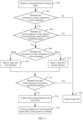
- a memory controller 106 may schedule memory memory accesss in batches. For example, a read access 1 to a read access N may be placed in a scheduling queue as a first batch of accesses 802, a read access N+1 to a read access 2N may be placed in the scheduling queue as a second batch of accesses 804, and a write access 1 to a write access N may be placed in the scheduling queue as a K th batch of accesses 806. Each batch may include a plurality of read accesses for accessing a same bank or a plurality of write accesses for accessing a same bank.
- Step 902 A memory controller performs an i th batch of accesses.
- An initial value of i may be set to 1, and i is a natural number greater than or equal to 1.
- the memory controller may schedule the plurality of memory access requests to the scheduling queue in batches based on types of the memory access requests. For example, the memory controller may schedule the plurality of memory access requests to the scheduling queue in the manner of scheduling in batches shown in FIG. 8 .
- the i th batch of accesses performed by the memory controller may be any batch of accesses shown in FIG. 8 .
- the i th batch of accesses may refer to the first batch of accesses 802, the second batch of accesses 804, or the K th batch of accesses 806.
- Step 904 The memory controller determines whether the i th batch of accesses are completely performed. Specifically, the memory controller may determine whether a performed access is a last access of the i th batch, to determine whether the i th batch of accesses are completely performed. Alternatively, the memory controller may determine, based on whether there is another access in the scheduling queue, whether the i th batch of accesses are completely performed. In addition, the memory controller may alternatively determine, in a counting manner, whether the i th batch of accesses are completely performed. A method for the memory controller to determine whether the i th batch of accesses are completely performed is not limited herein.
- step 904 the memory controller further determines whether to perform an (i+1) th batch of accesses. Specifically, the memory controller may determine, based on whether there is another access in the scheduling queue or the buffer queue, whether the (i+1) th batch of accesses need to be performed. If the (i+1) th batch of accesses need to be performed, the method proceeds to step 908. If it is determined that the (i+1) th batch of accesses do not need to be performed, it indicates that no other memory access needs to be performed, and the method proceeds to step 914.
- Step 908 The memory controller determines whether the i th batch of accesses and the (i+1) th batch of accesses are memory accesses of a same type.
- a same batch of memory accesses may be a plurality of memory access requests of a same type. Therefore, in this step, the memory controller may determine whether types of the i th batch of accesses and the (i+1) th batch of accesses are the same, for example, whether both the i th batch of accesses and the (i+1) th batch of accesses are read accesses or write accesses.
- step 910 If the i th batch of accesses and the (i+1) th batch of accesses are memory accesses of a same type, the method proceeds to step 910. If the i th batch of accesses and the (i+1) th batch of accesses are memory accesses of different types, the method proceeds to step 914.
- Step 910 The memory controller further determines whether both the i th batch of accesses and the (i+1) th batch of accesses are read accesses. If both the i th batch of accesses and the (i+1) th batch of accesses are read accesses, the method proceeds to step 912. If the i th batch of accesses or the (i+1) th batch of accesses are write accesses, the method proceeds to step 914.
- Step 912 The memory controller keeps a currently opened row in an open state.
- step 908 If it is determined in step 908 that the i th batch of accesses and the (i+1) th batch of accesses are memory accesses of different types, for example, the i th batch of accesses are write accesses, or the (i+1) th batch of accesses are write accesses.
- the memory controller needs to switch between the read access and the write access.
- randomness of the write access is higher.
- the method proceeds to step 914, to close all rows opened in a process of performing the i th batch of accesses. As shown in FIG.
- step 8 after the second batch of accesses 804 are completely performed, switching is performed to perform a next batch of accesses. If the next batch of accesses of the second batch of accesses 804 are write accesses (for example, when the next batch of accesses are the K th batch of accesses 806), all rows opened in a process of performing the second batch of accesses 804 are closed after the second batch of accesses 804 are completely performed. Then, the method proceeds to step 916 to perform the next batch of accesses.
- a quantity of times of switching between the read access and the write access can be further reduced.
- different row management policies can be used during switching between different batches of accesses, a row conflict that may be caused during switching between different batches can be further reduced, a latency caused by inappropriate closing of a memory row can be reduced, and a waste of bus bandwidth can be reduced.
- DMA read/write is usually read/write of a large data block, and a DMA is usually unidirectionally performed once.
- a data block that is being accessed by using the DMA is usually not accessed by another source.
- DMA read and write operations have a good locality and are irrelevant to another request. Therefore, a memory access policy in a DMA scenario may be considered separately. For example, in actual application, a DMA memory access and a non-DMA memory access may be scheduled in batches. In addition, DMA memory accesses may be further classified into a DMA read access and a DMA write access for scheduling in batches.
- an embodiment of the present invention further provides a memory controller.
- the memory controller includes a communications interface and a logic circuit that is configured to perform the memory management method in the foregoing embodiment.
- the communications interface is configured to receive a memory access sent by a processor of a computer system.
- the memory controller provided in this embodiment of the present invention may be shown as the memory controller 106 in FIG. 1 .
Landscapes
- Engineering & Computer Science (AREA)
- Theoretical Computer Science (AREA)
- Physics & Mathematics (AREA)
- General Engineering & Computer Science (AREA)
- General Physics & Mathematics (AREA)
- Human Computer Interaction (AREA)
- Software Systems (AREA)
- Microelectronics & Electronic Packaging (AREA)
- Computer Hardware Design (AREA)
- Dram (AREA)
- Memory System (AREA)
- Memory System Of A Hierarchy Structure (AREA)
Claims (14)
- Speicherverwaltungsverfahren, Folgendes umfassend:Empfangen (401) einer Speicherzugriffsanforderung;Bestimmen (403) eines Zugriffstyps der Speicherzugriffsanforderung, wobei der Zugriffstyp der Speicherzugriffsanforderung einen Lesezugriff oder einen Schreibzugriff umfasst; undAusführen (405) einer Zeilenverwaltungsrichtlinie, die dem Zugriffstyp der Speicherzugriffsanforderung entspricht, wobei die Zeilenverwaltungsrichtlinie eine Richtlinie zum Schließen einer geöffneten Zeile oder zum Schließen eines Zeilenpuffers umfasst, nachdem Daten einer Zeile in den Zeilenpuffer gelangen,wobei die Speicherzugriffsanforderung zu einem ersten Stapel von Speicherzugriffsanforderungen gehört und zum Zugreifen auf eine Zielzeile verwendet wird, und wobei das Verfahren ferner Folgendes umfasst:Bestimmen (904), dass der erste Stapel von Speicherzugriffsanforderungen vollständig durchgeführt wird und ein zweiter Stapel von Speicherzugriffsanforderungen durchzuführen ist, wobei die Zielzeile eine aktuell geöffnete Zeile ist; undHalten (912) der Zielzeile in dem offenen Zustand, wenn sowohl der erste Stapel von Speicherzugriffsanforderungen als auch der zweite Stapel von Speicherzugriffsanforderungen Lesezugriffsanforderungen sind;wenn sich ein Zugriffstyp des ersten Stapels von Speicherzugriffsanforderungen von einem Zugriffstyp des zweiten Stapels von Speicherzugriffsanforderungen unterscheidet, Schließen (914) der Zielzeile, falls der Zugriffstyp des ersten Stapels ein Lesezugriff ist und falls der Zugriffstyp des ersten Stapels ein Schreibzugriff ist.
- Verfahren nach Anspruch 1, wobei die Speicherzugriffsanforderung zum Zugreifen auf die Zielzeile in einer Zielspeicherbank in einem Speicher verwendet wird und das Ausführen einer Zeilenverwaltungsrichtlinie, die dem Zugriffstyp der Speicherzugriffsanforderung entspricht, Folgendes umfasst:
Ausführen einer Zeilenverwaltungsrichtlinie, die sich auf die Zielspeicherbank bezieht und dem Zugriffstyp der Speicherzugriffsanforderung entspricht, wobei der Speicher eine oder mehrere Speicherbänke umfasst und die Zielspeicherbank eine der einen oder mehreren Speicherbänke ist. - Verfahren nach Anspruch 2, ferner umfassend:
Anpassen der Zeilenverwaltungsrichtlinie basierend auf dem Zugriffstyp der Speicherzugriffsanforderung und einem Zeilentrefferstatus der Zielzeile. - Verfahren nach Anspruch 3, wobei das Anpassen der Zeilenverwaltungsrichtlinie der Zielspeicherbank basierend auf dem Zugriffstyp der Speicherzugriffsanforderung und einem Zeilentrefferstatus der Zielzeile Folgendes umfasst:
wenn die Speicherzugriffsanforderung ein Lesezugriff ist, Anpassen eines ersten Indikators der Zielspeicherbank basierend auf dem Zeilentrefferstatus der Zielzeile, wobei der erste Indikator angibt, ob die Zielzeile zu schließen ist, nachdem der Lesezugriff durchgeführt wurde. - Verfahren nach Anspruch 4, wobei das Anpassen der Zeilenverwaltungsrichtlinie der Zielspeicherbank basierend auf dem Zugriffstyp der Speicherzugriffsanforderung und einem Zeilentrefferstatus der Zielzeile ferner Folgendes umfasst:
wenn die Speicherzugriffsanforderung ein Schreibzugriff ist, Anpassen eines zweiten Indikators der Zielspeicherbank basierend auf dem Zeilentrefferstatus der Zielzeile, wobei der zweite Indikator angibt, ob die Zielzeile zu schließen ist, nachdem der Schreibzugriff durchgeführt wurde. - Verfahren nach Anspruch 5, wobei der Zeilentrefferstatus einen Zeilentreffer oder einen Zeilenkonflikt umfasst und das Anpassen eines ersten Indikators oder eines zweiten Indikators der Zielspeicherbank basierend auf dem Zeilentrefferstatus der Zielzeile Folgendes umfasst:wenn die Speicherzugriffsanforderung einen Zeilentreffer verursacht, Anpassen des ersten Indikators oder des zweiten Indikators an eine erste Angabe, wobei die erste Angabe angibt, dass die Zielzeile nicht geschlossen ist oder die Zielzeile in einem offenen Zustand gehalten wird; oderwenn die Speicherzugriffsanforderung einen Zeilenkonflikt verursacht, Anpassen des ersten Indikators oder des zweiten Indikators an eine zweite Angabe, wobei die zweite Angabe angibt, dass die Zielzeile geschlossen ist.
- Verfahren nach Anspruch 5 oder 6, wobei der Zeilentrefferstatus einen Zeilenleerlauf oder einen Zeilenkonflikt umfasst, und das Anpassen eines ersten Indikators oder eines zweiten Indikators basierend auf dem Zeilentrefferstatus der Zielzeile Folgendes umfasst:wenn die Speicherzugriffsanforderung einen Zeilenleerlauf verursacht, Bestimmen, ob die Speicherzugriffsanforderung einen Zeilentreffer verursacht hätte, wobei der Speicherzugriff einen Zeilenleerlauf verursacht, wenn bestimmt wird, dass in der Zielspeicherbank keine geöffnete Zeile vorhanden ist, und wobei der Speicherzugriff einen Zeilentreffer verursacht hätte, wenn eine Zeilenadresse des Speicherzugriffs dieselbe ist wie eine Zeilenadresse des vorherigen Speicherzugriffs; undwenn die Speicherzugriffsanforderung einen Zeilentreffer verursacht hätte, Anpassen des ersten Indikators oder des zweiten Indikators an die erste Angabe, wobei die erste Angabe angibt, dass die Zielzeile nicht geschlossen ist oder die Zielzeile in dem offenen Zustand gehalten wird, oderwenn die Speicherzugriffsanforderung einen Zeilenkonflikt verursacht, Anpassen des ersten Indikators oder des zweiten Indikators an die zweite Angabe, wobei die zweite Angabe angibt, dass die Zielzeile geschlossen ist, wobei ein Zeilenkonflikt verursacht wird, wenn die Zeilenadresse des Speicherzugriffs keine Adresse der geöffneten Zeile in der Zielspeicherbank ist.
- Verfahren nach einem der Ansprüche 5 bis 7, ferner umfassend:Bestimmen eines Zugriffstyps eines vorherigen Speicherzugriffs der Speicherzugriffsanforderung; undwobei das Anpassen eines ersten Indikators oder eines zweiten Indikators der Zielspeicherbank basierend auf dem Zeilentrefferstatus der Zielzeile Folgendes umfasst:
Anpassen des ersten Indikators oder des zweiten Indikators der Zielspeicherbank basierend auf dem Zeilentrefferstatus der Zielzeile und dem Zugriffstyp des vorherigen Speicherzugriffs des Speicherzugriffs. - Verfahren nach Anspruch 5, wobei
ein Anfangswert des ersten Indikators größer als ein Anfangswert des zweiten Indikators ist. - Verfahren nach Anspruch 7, wobeiwenn der erste Indikator angepasst wird, eine erste Anpassungsamplitude der Anpassung an die erste Angabe größer als eine zweite Anpassungsamplitude der Anpassung an die zweite Angabe ist; undwenn der zweite Indikator angepasst wird, eine dritte Anpassungsamplitude der Anpassung an die erste Angabe kleiner als eine vierte Anpassungsamplitude der Anpassung an die zweite Angabe ist.
- Verfahren nach Anspruch 4, wobei das Anpassen der Zeilenverwaltungsrichtlinie der Zielspeicherbank basierend auf dem Zugriffstyp der Speicherzugriffsanforderung und einem Zeilentrefferstatus der Zielzeile ferner Folgendes umfasst:
wenn der Zugriffstyp des Speicherzugriffs ein Schreibzugriff ist, Bestimmen, dass die Zeilenverwaltungsrichtlinie der Zielspeicherbank eine voreingestellte Zeilenverwaltungsrichtlinie ist, die dem Schreibzugriff entspricht, wobei die voreingestellte Zeilenverwaltungsrichtlinie angibt, ob die Zielzeile zu schließen ist, nachdem der Schreibzugriff durchgeführt wurde. - Speicherverwaltungsvorrichtung, Folgendes umfassend:einen Prozessor (104), der dazu konfiguriert ist, eine Speicherzugriffsanforderung zu senden; undeine Speichersteuerung (106), die zu Folgendem konfiguriert ist:Empfangen der Speicherzugriffsanforderung;Bestimmen eines Zugriffstyps der Speicherzugriffsanforderung, wobei der Zugriffstyp der Speicherzugriffsanforderung einen Lesezugriff oder einen Schreibzugriff umfasst; undAusführen einer Zeilenverwaltungsrichtlinie, die dem Zugriffstyp der Speicherzugriffsanforderung entspricht,wobei die Zeilenverwaltungsrichtlinie eine Richtlinie zum Schließen einer geöffneten Zeile oder zum Schließen eines Zeilenpuffers umfasst, nachdem Daten einer Zeile in den Zeilenpuffer gelangen,wobei die Speicherzugriffsanforderung zu einem ersten Stapel von Speicherzugriffsanforderungen gehört und zum Zugreifen auf eine Zielzeile verwendet wird und die Speichersteuerung ferner zu Folgendem konfiguriert ist:Bestimmen, dass der erste Stapel von Speicherzugriffsanforderungen vollständig durchgeführt wird und ein zweiter Stapel von Speicherzugriffsanforderungen durchzuführen ist, wobei die Zielzeile eine aktuell geöffnete Zeile ist; undHalten der Zielzeile in dem offenen Zustand, wenn sowohl der erste Stapel von Speicherzugriffsanforderungen als auch der zweite Stapel von Speicherzugriffsanforderungen Lesezugriffsanforderungen sind;wenn sich ein Zugriffstyp des ersten Stapels von Speicherzugriffsanforderungen von einem Zugriffstyp des zweiten Stapels von Speicherzugriffsanforderungen unterscheidet, Schließen der Zielzeile, falls der Zugriffstyp des ersten Stapels ein Lesezugriff ist und falls der Zugriffstyp des ersten Stapels ein Schreibzugriff ist.
- Vorrichtung nach Anspruch 12, wobei die Speicherzugriffsanforderung zum Zugreifen auf die Zielzeile in einer Zielspeicherbank in einem Speicher verwendet wird und die Speichersteuerung zu Folgendem konfiguriert ist:
Ausführen einer Zeilenverwaltungsrichtlinie, die sich auf die Zielspeicherbank bezieht und dem Zugriffstyp der Speicherzugriffsanforderung entspricht, wobei der Speicher eine oder mehrere Speicherbänke umfasst und die Zielspeicherbank eine der einen oder mehreren Speicherbänke ist. - Vorrichtung nach Anspruch 12 oder 13, wobei die Speichersteuerung ferner zu Folgendem konfiguriert ist:
Anpassen der Zeilenverwaltungsrichtlinie basierend auf dem Zugriffstyp der Speicherzugriffsanforderung und einem Zeilentrefferstatus der Zielzeile.
Applications Claiming Priority (3)
| Application Number | Priority Date | Filing Date | Title |
|---|---|---|---|
| CN202010693280 | 2020-07-17 | ||
| CN202011176594.3A CN113946435A (zh) | 2020-07-17 | 2020-10-28 | 内存管理技术及计算机系统 |
| PCT/CN2021/093982 WO2022012143A1 (zh) | 2020-07-17 | 2021-05-15 | 内存管理技术及计算机系统 |
Publications (3)
| Publication Number | Publication Date |
|---|---|
| EP4174666A1 EP4174666A1 (de) | 2023-05-03 |
| EP4174666A4 EP4174666A4 (de) | 2023-12-20 |
| EP4174666B1 true EP4174666B1 (de) | 2025-07-09 |
Family
ID=76296140
Family Applications (1)
| Application Number | Title | Priority Date | Filing Date |
|---|---|---|---|
| EP21842284.8A Active EP4174666B1 (de) | 2020-07-17 | 2021-05-15 | Speicherverwaltungstechnologie und computersystem |
Country Status (6)
| Country | Link |
|---|---|
| US (1) | US12455688B2 (de) |
| EP (1) | EP4174666B1 (de) |
| JP (1) | JP7553062B2 (de) |
| KR (1) | KR102749765B1 (de) |
| CN (1) | CN112965816B (de) |
| WO (1) | WO2022012143A1 (de) |
Family Cites Families (25)
| Publication number | Priority date | Publication date | Assignee | Title |
|---|---|---|---|---|
| US5889714A (en) * | 1997-11-03 | 1999-03-30 | Digital Equipment Corporation | Adaptive precharge management for synchronous DRAM |
| US6219765B1 (en) * | 1998-08-03 | 2001-04-17 | Micron Technology, Inc. | Memory paging control apparatus |
| US6219764B1 (en) * | 1998-08-03 | 2001-04-17 | Micron Technology, Inc. | Memory paging control method |
| US6212598B1 (en) * | 1998-11-30 | 2001-04-03 | Micron Technology, Inc. | Controlling a paging policy based on a requestor characteristic |
| US7127573B1 (en) * | 2000-05-04 | 2006-10-24 | Advanced Micro Devices, Inc. | Memory controller providing multiple power modes for accessing memory devices by reordering memory transactions |
| US6799241B2 (en) | 2002-01-03 | 2004-09-28 | Intel Corporation | Method for dynamically adjusting a memory page closing policy |
| US7133995B1 (en) * | 2002-12-16 | 2006-11-07 | Advanced Micro Devices, Inc. | Dynamic page conflict prediction for DRAM |
| US20050060533A1 (en) * | 2003-09-17 | 2005-03-17 | Steven Woo | Method, device, software and apparatus for adjusting a system parameter value, such as a page closing time |
| US7076617B2 (en) | 2003-09-30 | 2006-07-11 | Intel Corporation | Adaptive page management |
| US7587547B2 (en) | 2006-03-30 | 2009-09-08 | Intel Corporation | Dynamic update adaptive idle timer |
| CN101123113B (zh) * | 2007-09-20 | 2010-07-14 | 上海交通大学 | 同步动态随机访问存储器的访问方法及控制装置 |
| US20090157985A1 (en) * | 2007-12-18 | 2009-06-18 | Arm Limited | Accessing memory arrays |
| CN101488117B (zh) * | 2009-02-27 | 2013-01-30 | 无锡中星微电子有限公司 | 一种预充电数据访问控制装置和方法 |
| US20120059983A1 (en) * | 2010-09-03 | 2012-03-08 | David Wilkins Nellans | Predictor-based management of dram row-buffers |
| US20120297131A1 (en) * | 2011-05-20 | 2012-11-22 | Jaewoong Chung | Scheduling-Policy-Aware DRAM Page Management Mechanism |
| JP2013065150A (ja) * | 2011-09-16 | 2013-04-11 | Toshiba Corp | キャッシュメモリ装置、プロセッサ、および情報処理装置 |
| US9336855B2 (en) | 2013-05-14 | 2016-05-10 | Qualcomm Incorporated | Methods and systems for smart refresh of dynamic random access memory |
| CN103810123B (zh) * | 2014-02-18 | 2017-12-29 | 龙芯中科技术有限公司 | 内存控制装置及方法 |
| US10095437B2 (en) * | 2015-08-03 | 2018-10-09 | Intel Corporation | Memory access control |
| US10133493B2 (en) * | 2016-03-01 | 2018-11-20 | Marvell World Trade Ltd. | DRAM controller with adaptive precharge policy |
| CN106095698B (zh) * | 2016-06-03 | 2019-04-23 | 合一网络技术(北京)有限公司 | 面向对象的缓存写入、读取方法及装置 |
| US10331360B2 (en) * | 2016-09-29 | 2019-06-25 | Intel Corporation | Scalable bandwidth non-volatile memory |
| CN108959106B (zh) * | 2017-05-18 | 2020-12-18 | 华为技术有限公司 | 内存访问方法和装置 |
| CN111240582B (zh) | 2018-11-29 | 2022-01-28 | 长鑫存储技术有限公司 | 数据读写方法、读写装置和动态随机存储器 |
| CN111258925B (zh) * | 2020-01-20 | 2022-05-27 | 中国科学院微电子研究所 | 非易失内存的访问方法、装置、内存控制器、设备及介质 |
-
2020
- 2020-10-28 CN CN202110188761.4A patent/CN112965816B/zh active Active
-
2021
- 2021-05-15 WO PCT/CN2021/093982 patent/WO2022012143A1/zh not_active Ceased
- 2021-05-15 KR KR1020237005222A patent/KR102749765B1/ko active Active
- 2021-05-15 JP JP2023503053A patent/JP7553062B2/ja active Active
- 2021-05-15 EP EP21842284.8A patent/EP4174666B1/de active Active
-
2023
- 2023-01-13 US US18/154,532 patent/US12455688B2/en active Active
Also Published As
| Publication number | Publication date |
|---|---|
| JP7553062B2 (ja) | 2024-09-18 |
| CN112965816B (zh) | 2023-06-02 |
| US12455688B2 (en) | 2025-10-28 |
| KR102749765B1 (ko) | 2025-01-07 |
| CN112965816A (zh) | 2021-06-15 |
| WO2022012143A1 (zh) | 2022-01-20 |
| EP4174666A4 (de) | 2023-12-20 |
| JP2023534052A (ja) | 2023-08-07 |
| KR20230037649A (ko) | 2023-03-16 |
| US20230152977A1 (en) | 2023-05-18 |
| EP4174666A1 (de) | 2023-05-03 |
Similar Documents
| Publication | Publication Date | Title |
|---|---|---|
| US11593027B2 (en) | Command selection policy with read priority | |
| US12153529B2 (en) | Memory system and computing system including the same | |
| CN110520929B (zh) | 内存刷新方法、装置及计算机系统 | |
| US20250328249A1 (en) | Adjustable timer component for semiconductor devices | |
| US20190026028A1 (en) | Minimizing performance degradation due to refresh operations in memory sub-systems | |
| WO2018188085A1 (zh) | 内存刷新技术及计算机系统 | |
| CN106024052A (zh) | 存储器控制器和存储器系统的控制方法 | |
| KR20230082529A (ko) | 리프레쉬 동작에서 파워 노이즈를 감소시킨 메모리 장치 및 그 동작방법 | |
| Liu et al. | LAMS: A latency-aware memory scheduling policy for modern DRAM systems | |
| EP4174666B1 (de) | Speicherverwaltungstechnologie und computersystem | |
| CN113946435A (zh) | 内存管理技术及计算机系统 | |
| US11526278B2 (en) | Adaptive page close prediction | |
| US12056371B2 (en) | Memory device having reduced power noise in refresh operation and operating method thereof | |
| US12417024B2 (en) | Transforming all-bank processing-in-memory operations into multiple masked processing-in-memory operations | |
| US20260017203A1 (en) | Cache and control method therefor, and computer system | |
| US20250348343A1 (en) | Devices and methods for traffic shaping arbitration to fetch commands from a host with multiple virtual machines | |
| US20260029956A1 (en) | Communications between a Memory Sub-System and a Host System to Identify Counts of Commands in Submission Queues | |
| US20260029957A1 (en) | Scalable Techniques to Process Separate Queues of Storage Access Commands from a Host System to a Memory Sub-System | |
| CN119829481A (zh) | 一种页面配置方法、ddr控制器及片上系统 | |
| WO2026024507A1 (en) | In-memory queue status array configured to identify queuing of commands in submission queues for communications between a memory sub-system and a host system | |
| WO2025006245A1 (en) | Row activation indication registers | |
| CN118869590A (zh) | 查表系统、设备以及集群 |
Legal Events
| Date | Code | Title | Description |
|---|---|---|---|
| STAA | Information on the status of an ep patent application or granted ep patent |
Free format text: STATUS: THE INTERNATIONAL PUBLICATION HAS BEEN MADE |
|
| PUAI | Public reference made under article 153(3) epc to a published international application that has entered the european phase |
Free format text: ORIGINAL CODE: 0009012 |
|
| STAA | Information on the status of an ep patent application or granted ep patent |
Free format text: STATUS: REQUEST FOR EXAMINATION WAS MADE |
|
| 17P | Request for examination filed |
Effective date: 20230125 |
|
| AK | Designated contracting states |
Kind code of ref document: A1 Designated state(s): AL AT BE BG CH CY CZ DE DK EE ES FI FR GB GR HR HU IE IS IT LI LT LU LV MC MK MT NL NO PL PT RO RS SE SI SK SM TR |
|
| DAV | Request for validation of the european patent (deleted) | ||
| DAX | Request for extension of the european patent (deleted) | ||
| A4 | Supplementary search report drawn up and despatched |
Effective date: 20231116 |
|
| RIC1 | Information provided on ipc code assigned before grant |
Ipc: G06F 9/50 20060101ALI20231113BHEP Ipc: G11C 11/4076 20060101ALI20231113BHEP Ipc: G11C 7/22 20060101ALI20231113BHEP Ipc: G06F 12/02 20060101ALI20231113BHEP Ipc: G06F 13/16 20060101AFI20231113BHEP |
|
| GRAP | Despatch of communication of intention to grant a patent |
Free format text: ORIGINAL CODE: EPIDOSNIGR1 |
|
| STAA | Information on the status of an ep patent application or granted ep patent |
Free format text: STATUS: GRANT OF PATENT IS INTENDED |
|
| INTG | Intention to grant announced |
Effective date: 20250117 |
|
| GRAS | Grant fee paid |
Free format text: ORIGINAL CODE: EPIDOSNIGR3 |
|
| GRAA | (expected) grant |
Free format text: ORIGINAL CODE: 0009210 |
|
| STAA | Information on the status of an ep patent application or granted ep patent |
Free format text: STATUS: THE PATENT HAS BEEN GRANTED |
|
| AK | Designated contracting states |
Kind code of ref document: B1 Designated state(s): AL AT BE BG CH CY CZ DE DK EE ES FI FR GB GR HR HU IE IS IT LI LT LU LV MC MK MT NL NO PL PT RO RS SE SI SK SM TR |
|
| REG | Reference to a national code |
Ref country code: GB Ref legal event code: FG4D |
|
| REG | Reference to a national code |
Ref country code: CH Ref legal event code: EP |
|
| REG | Reference to a national code |
Ref country code: IE Ref legal event code: FG4D |
|
| REG | Reference to a national code |
Ref country code: DE Ref legal event code: R096 Ref document number: 602021033942 Country of ref document: DE |
|
| REG | Reference to a national code |
Ref country code: NL Ref legal event code: MP Effective date: 20250709 |
|
| PG25 | Lapsed in a contracting state [announced via postgrant information from national office to epo] |
Ref country code: PT Free format text: LAPSE BECAUSE OF FAILURE TO SUBMIT A TRANSLATION OF THE DESCRIPTION OR TO PAY THE FEE WITHIN THE PRESCRIBED TIME-LIMIT Effective date: 20251110 |
|
| PG25 | Lapsed in a contracting state [announced via postgrant information from national office to epo] |
Ref country code: NL Free format text: LAPSE BECAUSE OF FAILURE TO SUBMIT A TRANSLATION OF THE DESCRIPTION OR TO PAY THE FEE WITHIN THE PRESCRIBED TIME-LIMIT Effective date: 20250709 |
|
| REG | Reference to a national code |
Ref country code: AT Ref legal event code: MK05 Ref document number: 1812483 Country of ref document: AT Kind code of ref document: T Effective date: 20250709 |
|
| PG25 | Lapsed in a contracting state [announced via postgrant information from national office to epo] |
Ref country code: IS Free format text: LAPSE BECAUSE OF FAILURE TO SUBMIT A TRANSLATION OF THE DESCRIPTION OR TO PAY THE FEE WITHIN THE PRESCRIBED TIME-LIMIT Effective date: 20251109 |
|
| PG25 | Lapsed in a contracting state [announced via postgrant information from national office to epo] |
Ref country code: NO Free format text: LAPSE BECAUSE OF FAILURE TO SUBMIT A TRANSLATION OF THE DESCRIPTION OR TO PAY THE FEE WITHIN THE PRESCRIBED TIME-LIMIT Effective date: 20251009 |
|
| REG | Reference to a national code |
Ref country code: LT Ref legal event code: MG9D |
|
| PG25 | Lapsed in a contracting state [announced via postgrant information from national office to epo] |
Ref country code: AT Free format text: LAPSE BECAUSE OF FAILURE TO SUBMIT A TRANSLATION OF THE DESCRIPTION OR TO PAY THE FEE WITHIN THE PRESCRIBED TIME-LIMIT Effective date: 20250709 |
|
| PG25 | Lapsed in a contracting state [announced via postgrant information from national office to epo] |
Ref country code: FI Free format text: LAPSE BECAUSE OF FAILURE TO SUBMIT A TRANSLATION OF THE DESCRIPTION OR TO PAY THE FEE WITHIN THE PRESCRIBED TIME-LIMIT Effective date: 20250709 |
|
| PG25 | Lapsed in a contracting state [announced via postgrant information from national office to epo] |
Ref country code: HR Free format text: LAPSE BECAUSE OF FAILURE TO SUBMIT A TRANSLATION OF THE DESCRIPTION OR TO PAY THE FEE WITHIN THE PRESCRIBED TIME-LIMIT Effective date: 20250709 |
|
| PG25 | Lapsed in a contracting state [announced via postgrant information from national office to epo] |
Ref country code: GR Free format text: LAPSE BECAUSE OF FAILURE TO SUBMIT A TRANSLATION OF THE DESCRIPTION OR TO PAY THE FEE WITHIN THE PRESCRIBED TIME-LIMIT Effective date: 20251010 |
|
| PG25 | Lapsed in a contracting state [announced via postgrant information from national office to epo] |
Ref country code: SE Free format text: LAPSE BECAUSE OF FAILURE TO SUBMIT A TRANSLATION OF THE DESCRIPTION OR TO PAY THE FEE WITHIN THE PRESCRIBED TIME-LIMIT Effective date: 20250709 |
|
| PG25 | Lapsed in a contracting state [announced via postgrant information from national office to epo] |
Ref country code: LV Free format text: LAPSE BECAUSE OF FAILURE TO SUBMIT A TRANSLATION OF THE DESCRIPTION OR TO PAY THE FEE WITHIN THE PRESCRIBED TIME-LIMIT Effective date: 20250709 |
|
| PG25 | Lapsed in a contracting state [announced via postgrant information from national office to epo] |
Ref country code: BG Free format text: LAPSE BECAUSE OF FAILURE TO SUBMIT A TRANSLATION OF THE DESCRIPTION OR TO PAY THE FEE WITHIN THE PRESCRIBED TIME-LIMIT Effective date: 20250709 Ref country code: PL Free format text: LAPSE BECAUSE OF FAILURE TO SUBMIT A TRANSLATION OF THE DESCRIPTION OR TO PAY THE FEE WITHIN THE PRESCRIBED TIME-LIMIT Effective date: 20250709 |
|
| PG25 | Lapsed in a contracting state [announced via postgrant information from national office to epo] |
Ref country code: RS Free format text: LAPSE BECAUSE OF FAILURE TO SUBMIT A TRANSLATION OF THE DESCRIPTION OR TO PAY THE FEE WITHIN THE PRESCRIBED TIME-LIMIT Effective date: 20251009 |
|
| PG25 | Lapsed in a contracting state [announced via postgrant information from national office to epo] |
Ref country code: ES Free format text: LAPSE BECAUSE OF FAILURE TO SUBMIT A TRANSLATION OF THE DESCRIPTION OR TO PAY THE FEE WITHIN THE PRESCRIBED TIME-LIMIT Effective date: 20250709 |