EP4173046B1 - Verfahren zur bildung einer anzeige - Google Patents
Verfahren zur bildung einer anzeige Download PDFInfo
- Publication number
- EP4173046B1 EP4173046B1 EP21737742.3A EP21737742A EP4173046B1 EP 4173046 B1 EP4173046 B1 EP 4173046B1 EP 21737742 A EP21737742 A EP 21737742A EP 4173046 B1 EP4173046 B1 EP 4173046B1
- Authority
- EP
- European Patent Office
- Prior art keywords
- light emitting
- emitting diode
- dies
- backplane
- bond
- Prior art date
- Legal status (The legal status is an assumption and is not a legal conclusion. Google has not performed a legal analysis and makes no representation as to the accuracy of the status listed.)
- Active
Links
Images

Classifications
-
- H—ELECTRICITY
- H10—SEMICONDUCTOR DEVICES; ELECTRIC SOLID-STATE DEVICES NOT OTHERWISE PROVIDED FOR
- H10H—INORGANIC LIGHT-EMITTING SEMICONDUCTOR DEVICES HAVING POTENTIAL BARRIERS
- H10H20/00—Individual inorganic light-emitting semiconductor devices having potential barriers, e.g. light-emitting diodes [LED]
- H10H20/01—Manufacture or treatment
-
- H—ELECTRICITY
- H10—SEMICONDUCTOR DEVICES; ELECTRIC SOLID-STATE DEVICES NOT OTHERWISE PROVIDED FOR
- H10H—INORGANIC LIGHT-EMITTING SEMICONDUCTOR DEVICES HAVING POTENTIAL BARRIERS
- H10H20/00—Individual inorganic light-emitting semiconductor devices having potential barriers, e.g. light-emitting diodes [LED]
- H10H20/01—Manufacture or treatment
- H10H20/011—Manufacture or treatment of bodies, e.g. forming semiconductor layers
- H10H20/013—Manufacture or treatment of bodies, e.g. forming semiconductor layers having light-emitting regions comprising only Group III-V materials
- H10H20/0137—Manufacture or treatment of bodies, e.g. forming semiconductor layers having light-emitting regions comprising only Group III-V materials the light-emitting regions comprising nitride materials
-
- H—ELECTRICITY
- H10—SEMICONDUCTOR DEVICES; ELECTRIC SOLID-STATE DEVICES NOT OTHERWISE PROVIDED FOR
- H10H—INORGANIC LIGHT-EMITTING SEMICONDUCTOR DEVICES HAVING POTENTIAL BARRIERS
- H10H20/00—Individual inorganic light-emitting semiconductor devices having potential barriers, e.g. light-emitting diodes [LED]
- H10H20/01—Manufacture or treatment
- H10H20/011—Manufacture or treatment of bodies, e.g. forming semiconductor layers
- H10H20/018—Bonding of wafers
-
- H—ELECTRICITY
- H10—SEMICONDUCTOR DEVICES; ELECTRIC SOLID-STATE DEVICES NOT OTHERWISE PROVIDED FOR
- H10H—INORGANIC LIGHT-EMITTING SEMICONDUCTOR DEVICES HAVING POTENTIAL BARRIERS
- H10H20/00—Individual inorganic light-emitting semiconductor devices having potential barriers, e.g. light-emitting diodes [LED]
- H10H20/01—Manufacture or treatment
- H10H20/036—Manufacture or treatment of packages
- H10H20/0364—Manufacture or treatment of packages of interconnections
-
- H—ELECTRICITY
- H10—SEMICONDUCTOR DEVICES; ELECTRIC SOLID-STATE DEVICES NOT OTHERWISE PROVIDED FOR
- H10H—INORGANIC LIGHT-EMITTING SEMICONDUCTOR DEVICES HAVING POTENTIAL BARRIERS
- H10H20/00—Individual inorganic light-emitting semiconductor devices having potential barriers, e.g. light-emitting diodes [LED]
- H10H20/80—Constructional details
- H10H20/81—Bodies
-
- H—ELECTRICITY
- H10—SEMICONDUCTOR DEVICES; ELECTRIC SOLID-STATE DEVICES NOT OTHERWISE PROVIDED FOR
- H10H—INORGANIC LIGHT-EMITTING SEMICONDUCTOR DEVICES HAVING POTENTIAL BARRIERS
- H10H20/00—Individual inorganic light-emitting semiconductor devices having potential barriers, e.g. light-emitting diodes [LED]
- H10H20/80—Constructional details
- H10H20/83—Electrodes
- H10H20/832—Electrodes characterised by their material
- H10H20/833—Transparent materials
-
- H—ELECTRICITY
- H10—SEMICONDUCTOR DEVICES; ELECTRIC SOLID-STATE DEVICES NOT OTHERWISE PROVIDED FOR
- H10H—INORGANIC LIGHT-EMITTING SEMICONDUCTOR DEVICES HAVING POTENTIAL BARRIERS
- H10H20/00—Individual inorganic light-emitting semiconductor devices having potential barriers, e.g. light-emitting diodes [LED]
- H10H20/80—Constructional details
- H10H20/83—Electrodes
- H10H20/832—Electrodes characterised by their material
- H10H20/835—Reflective materials
-
- H—ELECTRICITY
- H10—SEMICONDUCTOR DEVICES; ELECTRIC SOLID-STATE DEVICES NOT OTHERWISE PROVIDED FOR
- H10H—INORGANIC LIGHT-EMITTING SEMICONDUCTOR DEVICES HAVING POTENTIAL BARRIERS
- H10H29/00—Integrated devices, or assemblies of multiple devices, comprising at least one light-emitting semiconductor element covered by group H10H20/00
- H10H29/10—Integrated devices comprising at least one light-emitting semiconductor component covered by group H10H20/00
- H10H29/14—Integrated devices comprising at least one light-emitting semiconductor component covered by group H10H20/00 comprising multiple light-emitting semiconductor components
- H10H29/142—Two-dimensional arrangements, e.g. asymmetric LED layout
-
- H—ELECTRICITY
- H10—SEMICONDUCTOR DEVICES; ELECTRIC SOLID-STATE DEVICES NOT OTHERWISE PROVIDED FOR
- H10W—GENERIC PACKAGES, INTERCONNECTIONS, CONNECTORS OR OTHER CONSTRUCTIONAL DETAILS OF DEVICES COVERED BY CLASS H10
- H10W90/00—Package configurations
-
- H—ELECTRICITY
- H10—SEMICONDUCTOR DEVICES; ELECTRIC SOLID-STATE DEVICES NOT OTHERWISE PROVIDED FOR
- H10H—INORGANIC LIGHT-EMITTING SEMICONDUCTOR DEVICES HAVING POTENTIAL BARRIERS
- H10H20/00—Individual inorganic light-emitting semiconductor devices having potential barriers, e.g. light-emitting diodes [LED]
- H10H20/80—Constructional details
- H10H20/84—Coatings, e.g. passivation layers or antireflective coatings
-
- H—ELECTRICITY
- H10—SEMICONDUCTOR DEVICES; ELECTRIC SOLID-STATE DEVICES NOT OTHERWISE PROVIDED FOR
- H10H—INORGANIC LIGHT-EMITTING SEMICONDUCTOR DEVICES HAVING POTENTIAL BARRIERS
- H10H20/00—Individual inorganic light-emitting semiconductor devices having potential barriers, e.g. light-emitting diodes [LED]
- H10H20/80—Constructional details
- H10H20/85—Packages
- H10H20/857—Interconnections, e.g. lead-frames, bond wires or solder balls
Definitions
- the invention relates to the formation of a display.
- the invention relates to a method of forming a monolithic-based micro LED display with the facility to replace pixels.
- LED devices Light emitting diode (LED) devices are known to provide highly efficient and controllable light sources for display applications.
- LED devices are known to provide highly efficient and controllable light sources for display applications.
- the implementation of LED devices into micro LED arrays with small pixels at an ultra-fine pitch enables the production of high resolution displays.
- the presence of any defective LED devices in such arrays can be problematic.
- the number of dead pixels e.g., defective LED devices in a micro LED array
- the number of dead pixels is preferably less than 2 dead pixels per 2 million pixels (i.e., a successful yield of 99.9999%) in order to provide an acceptable display.
- redundancy schemes are known to be implemented, where back-up devices are provided in an LED array in order to provide light to pixels where there is a failure of any device.
- redundancy schemes use additional space, which affects the provision of closely packed, small, LED devices (dies) and hence pixels in micro LED displays.
- Document WO 2019/079381 A1 discloses a monolithic ultra-dense light emitting diode display having a dielectric material that insulates sidewalls of a P-type layer and an active layer from a reflective metal, and electrically contacts an N-type layer of a pillar, and further discloses a method of forming said display.
- a display comprising: a backplane comprising a plurality of backplane electrical contacts bonded to a plurality of physically isolated light emitting diode dies having an electrical contact, wherein at least one of the plurality of backplane electrical contacts is bonded to a corresponding electrical contact of the plurality of physically isolated light emitting diode dies using a reversible bond, thereby to enable removal and/or replacement of at least one physically isolated light emitting diode die by reversing the reversible bond between the at least one backplane electrical contact and the corresponding electrical contact of the plurality of physically isolated light emitting diode dies, wherein the plurality of physically isolated light emitting diode dies are formed from a monolithic light emitting diode structure.
- the formation of a display by bonding a backplane to a monolithic light emitting diode structure, removing material and forming reversible bonds between at least one of a plurality of backplane electrical contacts and the corresponding electrical contact of the monolithic light emitting diode structure means that individual LED dies can be identified and replaced, thereby ensuring that a sufficiently high yield of functional devices is present in a display without requiring space to be used for redundancy.
- arrays of light emitting pixels can be provided in a high resolution display with the facility to replace individual light emitting diode device dies, where required.
- the at least one of the backplane electrical contacts is reversibly bonded to the corresponding electrical contact of the monolithic light emitting diode structure using metal-to-metal bonding and/or eutectic bonding.
- bonding facilitates removal and replacement of LED devices whilst providing the electrical conductivity to form functioning devices and whilst providing a reflective surface to aid light extraction from individual LED devices.
- the method comprises: removing at least one physically isolated light emitting diode die; and replacing the at least one physically isolated light emitting diode die with a different one or more light emitting diode dies.
- the display is adapted to provide light emission from individual light emitting devices in an array with a preferred arrangement of light emission properties.
- the method comprises: removing at least one physically isolated light emitting diode die comprises increasing the temperature of the display thereby to enable removal of the at least one physically isolated light emitting diode die at the reversible bond between the backplane electrical contact and the corresponding electrical contact associated with the monolithic light emitting diode structure, preferably wherein increasing the temperature of the display comprises increasing the temperature at the reversible bond to surpass a eutectic temperature of the reversible bond, preferably wherein the reversible bond comprises at least one of a AuSn eutectic bond, a CuSn eutectic bond and a InSn eutectic bond.
- a controllable method is presented that simultaneously enables electrical conductivity, reversible bonding and relatively high reflectivity for enhanced light extraction.
- removing at least one physically isolated light emitting diode die comprises overcoming an electrostatic force of the reversible bond, preferably wherein the electrostatic force of the reversible bond is the electrostatic force of at least one of a Au-Au metal bond and a Cu-Cu metal bond.
- metal-metal bonds can be provided that simultaneously enable electrical conductivity, reversible bonding and relatively high reflectivity for enhanced light extraction.
- the method comprises: testing at least one of the plurality of physically isolated light emitting diode dies; identifying one or more defective light emitting diode dies; removing defective light emitting diode dies; and replacing the one or more removed light emitting diode dies.
- displays with high yields of working devices are provided based on monolithically grown LED devices, thereby providing high resolution displays.
- the method comprises: forming a conformal metal layer on at least a portion of the physically isolated light emitting diode dies, thereby to reduce optical cross talk between physically isolated light emitting diode dies.
- a conformal metal layer on at least a portion of the physically isolated light emitting diode dies, thereby to reduce optical cross talk between physically isolated light emitting diode dies.
- light extraction from individual LED dies is enhanced and the contrast between pixels associated with LED dies is improved.
- the method comprises: forming a transparent electrically conductive layer on the plurality of isolated light emitting diode dies, thereby to provide a common electrode.
- a transparent electrically conductive layer on the plurality of isolated light emitting diode dies, thereby to provide a common electrode.
- multiple devices in an array are simultaneously contacted thereby efficiently processing large numbers of devices.
- the method comprises: forming one or more magnetic metal regions associated with at least one of the physically isolated light emitting diode dies, thereby to facilitate removal of physically isolated light emitting diode dies.
- removal of individually dies is enhanced by the use of magnetic materials, thereby overcoming any residual forces to aid removal of individual LED devices.
- At least one of the reversible bonds is at least partially laterally surrounded by a dielectric layer thereby to separate the backplane and the monolithic light emitting diode structure, preferably wherein the dielectric layer comprises at least one of SiO 2 , Si 3 N 4 , Su-8, SrF 2 , PDMS and PMMA.
- the dielectric layer enables uniform processing without preventing removal of individual LED dies.
- the plurality of contacts of the monolithic light emitting structure comprises a high reflectivity metal, preferably wherein the high reflectivity metal is one of nickel (Ni) and silver (Ag).
- the high reflectivity metal is one of nickel (Ni) and silver (Ag).
- Ni nickel
- Ag silver
- such metal simultaneously provides electric conductivity whilst aiding light extraction.
- removing material from the monolithic light emitting diode structure comprises forming a discontinuity in at least one layer of the monolithic light emitting diode structure, preferably wherein the at least one layer of the monolithic light emitting diode structure is an n-type layer, more preferably wherein the n-type layer is an n-doped gallium nitride layer.
- forming discontinuities enables removal and replacement of individual, physically isolated dies.
- the method and structure enables display arrays of pixels to be provided, where the e.g., where the light emitting surface area of each pixel is less than or equal to 100 ⁇ m 2 , and preferably less than or equal to 16 ⁇ m 2 , and where the pixel pitch is less than 10 ⁇ m and preferably less than 4 ⁇ m and more preferably less than 3 ⁇ m.
- the method and structure described here is used to replace defective dies, in further examples it is used to provide LED dies in the array that are configured to emit light of a different wavelength to the dies formed in the monolithically grown array of LED devices.
- LED dies in the array that are configured to emit light of a different wavelength to the dies formed in the monolithically grown array of LED devices.
- Gallium arsenide (GaAs) based materials are a more established technology for red-light emitting LED dies. Therefore, in an example, the method described herein is used to replace LED dies in monolithically grown arrays of nitride-based LED dies to provide light of different wavelengths.
- the number of dies that would be transferred into the monolithically grown array is much less than the total number of dies in the array, providing a more efficient and practical
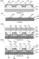
- Figure 1A a cross sectional view of an epitaxial crystalline structure 100A.
- the epitaxial crystalline structure 100A is a structure formed from crystalline layers sequentially grown or deposited to provide a light emitting structure.
- the epitaxial crystalline structure 100A is provided using metal organic chemical vapour deposition (MOCVD).
- MOCVD metal organic chemical vapour deposition
- alternative and/or additional methods of growth and/or deposition are used to provide the epitaxial crystalline structure 100A, for example molecular beam epitaxy (MBE).
- MBE molecular beam epitaxy
- the epitaxial crystalline structure 100A is provided in a continuous growth process and has a high crystalline quality and low defect density.
- the epitaxial structure 100A is provided using multiple growth steps that enable the selective provision of particular qualities, for example different wavelengths of light emission upon radiative recombination of carriers from different areas of the epitaxial crystalline structure 100A.
- a growth substrate 102 upon which there is grown an n-type region 104.
- the growth substrate 102 is a silicon substrate. Alternatively, in further examples different material is used in order to provide a growth substrate 102.
- the n-type region 104 is formed from n-type doped gallium nitride (GaN). In further examples, the n-type region 104 is formed from additional and/or alternative layers. For example, further buffer layers are included.
- an active region 106 On top of the n-type region 104 there is shown an active region 106.
- the active region 106 is configured to emit light following the recombination of carriers injected from n-type and p-type regions.
- the active region 106 includes a multiple quantum well (MQW) structure.
- MQW multiple quantum well
- the active region includes a single quantum well (SQW) structure.
- the active region 106 is configured to emit light with a primary peak wavelength that is controlled.
- different portions of the active region 106 are configured to emit light with different primary peak wavelengths.
- the p-type region 108 is formed from p-type doped GaN. In further examples, the p-type region 108 is formed from additional and/or alternative layers.
- the epitaxial crystalline structure 100A is based on group III-V material (such as III-nitride material, e.g. GaN based materials). Whilst the structure is shown to be a nitride based structure, in further example different materials are used to provide a monolithic array of light emitting devices. Whilst the n-type region 104, active region 106 and p-type region 108 are shown, the skilled person understands in further examples further layers and/or alternative layers are used in order to provide the epitaxial crystalline structure 100A.
- the epitaxial crystalline structure 100A is processed in order to form multiple monolithically grown LED devices. This is shown at Figure 1B.
- Figure 1B shows a cross sectional view of a processed structure 100B based on the epitaxial crystalline structure 100A of Figure 1A , where mesas 110 have been formed.
- the mesas 110 each include portions of the p-type region 108 and the active region 106.
- the mesas 110 are shown to have been formed on the n-type region 104.
- the mesas 110 are formed by selectively patterning and etching the epitaxial crystalline structure 100A using known techniques. The skilled person understands that alternatively and/or additionally the mesas 110 are formed from different and/or additional layers.
- Figure 1C shows a cross sectional view of a processed structure 100C that is a processed version of the structure 100B of Figure 1B .
- a conformal layer 112 formed on the mesas 110.
- the conformal layer 112 is deposited using known deposition techniques and is formed such that irreversible bonding with other layers is avoided at a later stage.
- the conformal layer 112 is dielectric layer formed from silicon dioxide (SiO 2 ).
- the conformal layer is a dielectric layer formed from a different material such as silicon nitride (Si 3 N 4 ), photoresist such as Su-8, strontium fluoride (SrF 2 ), polydimethylsiloxane (PDMS) or poly(methyl methacrylate) (PMMA).
- a different material such as silicon nitride (Si 3 N 4 ), photoresist such as Su-8, strontium fluoride (SrF 2 ), polydimethylsiloxane (PDMS) or poly(methyl methacrylate) (PMMA).
- the, or any other suitable material that enables reversible bonding at contacts without bonding by the portion of the conformal layer 112 that contacts a backplane to which the eventual structure is bonded.
- the conformal layer 112 is further processed in order to provide contacts to the p-type region 108.
- Figure 1D shows a cross sectional view of a processed epitaxial structure 100D that is a processed version of the structure 100C described with respect to Figure 1C .
- the structure 100C of Figure 1C is processed in order selectively to pattern and etch windows through the conformal layer 112, thereby to expose at least a portion of each of the mesas 110 to which p-type contacts with the p-type region 108 are to be formed. Once the windows have been provided, p-type contacts are 114 are formed in the windows on the mesas 110.
- the electrical p-type contacts 114 are formed from a metal.
- the metal is relatively highly reflective.
- the use of a relatively highly reflective electrical p-type contact 114 aids light extraction from the individual LED dies that are formed based on the mesas 110 of the monolithically grown structural 100.
- the electrical p-type contacts 114 are formed in order to enable metal bonding (such as gold to gold (Au-Au) or copper to copper (Cu-Cu) bonding) and eutectic bonding (gold-tin (Au-Sn), copper-tin (Cu-Sn), indium-tin (InSn)) with a backplane.
- the electrical p-type contacts 114 are formed from any suitability reflective and conductive material that can be used to form a reversible bond.
- the electrical p-type contacts 114 are formed from nickel and/or silver. The electrical p-type contacts 114 are used to form reversible bonds with a further backplane device and are therefore formed from a material that facilitates such reversible bonding. This is described in more detail below.
- FIG. 1E there is shown a cross sectional view of a structure 100E that is the epitaxial structure 100D of Figure 1D that has been processed further in order to planiarise the structure.
- FIG. 1E there is shown material 116 deposited into the gaps formed between the mesas 110, the surface of which has been planarised. Such planarization is achieved by deposition and chemical mechanical polishing of the material 116 to form a planar surface suitable for bonding to a further device. In further examples, alternative and/or additional methods are used in order to planarise the surface opposite the growth substrate 102.
- the material 116 is a metal. Further examples, alternative and/or additional material 116 is used, such as dielectric material.
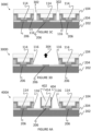
- Figure 2 illustrates a processed backplane 200 that has been processed in order to reversibly bond to a monolithically grown LED array, such as that described above with respect to Figure 1 .
- FIG. 2 shows a CMOS backplane 202 upon which a dielectric layer 204 has been deposited.
- the dielectric layer 204 is processed in order to pattern and selectively etch windows in which material is deposited to form electrical backplane contacts 206 using known techniques.
- the formation of windows exposes portions of the CMOS backplane 202 to which p-type contacts can be connected in order to control light emission from individual LED devices of in an array of LED devices.
- the backplane 202 is a CMOS backplane 202, in further examples, additional and/or alternative backplanes are used to bond with an LED based structure to form a functioning display.
- the backplane contacts 206 are designed to form a reversible bond with the electrical p-type contacts 114 of the structure 100E shown at Figure 1E . Accordingly, the backplane contacts 206 are formed in order to enable metal bonding (such as gold to gold (Au-Au) or copper to copper (Cu-Cu) bonding) and eutectic bonding (such as gold-tin (Au-Sn), copper-tin (Cu-Sn), indium-tin (InSn)). Accordingly, the combination of material used to form the p-type contacts 114 of the structure 100E shown at Figure 1E and the electrical backplane contacts 206 is chosen to provide a combination of material that provides a reversible bond.
- metal bonding such as gold to gold (Au-Au) or copper to copper (Cu-Cu) bonding
- eutectic bonding such as gold-tin (Au-Sn), copper-tin (Cu-Sn), indium-tin (InSn)
- the dielectric layer 204 is formed from silicon dioxide. Alternatively, and/or additionally the dielectric layer 204 is formed from silicon nitride, Su-8, SrF 2 , PDMS, PMMA or any other suitable material.
- the dielectric layer 204 is formed such that it contacts with the conformal layer 112 and accordingly the aim is to prevent an oxide-oxide combination during bonding, such that the dielectric layer 204 does not form an irreversible bond with the conformal layer 112. Accordingly, the combination of material used to form the conformal layer 112 and the dielectric layer 204 is chosen to provide a combination of material that provides a reversible bond at the electrical contacts and not at other portions of the interface between the processed backplane 200 and the monolithically grown epitaxial structure 100E.
- the structure 300A of Figure 3A shows a cross sectional view of the structure 100E of Figure 1E bonded to the processed structure 200 of Figure 2 .
- the structure 100E and the processed structure 200 are bonded using thermocompression bonding techniques.
- additional and/or alternative techniques are used to bond the structures 100E, 200.
- the electrical p-type contacts 114 are aligned with the backplane contacts 206 of the processed backplane 200.
- the combined structure 300A is shown in cross-section, the skilled person understands that the process is used for two dimensional arrays of LED devices that are monolithically grown on growth substrate 102 and bonded to a planar surface of a processed backplane 200.
- the electrical p-type contacts 114 of the monolithically grown LED array are arranged in order to coincide with backplane contacts 206 of the backplane 200 thereby to form reversible bonds between the p-type contacts 114 of the monolithically grown LED array and the backplane contacts 206 of the backplane 200.
- FIG. 3B shows a structure 300B which is the structure 300A of Figure 3A that has been processed in order to remove the growth substrate 102.
- the n-type region 104 is exposed and can be selectively patterned and etched using known techniques. This is shown at Figure 3C .
- Figure 3C shows a cross sectional view of a structure 300C that is the structure 300B of Figure 3B that has been processed further in order selectively to etch through the n-type region 104, the conformal layer 112 and the planarising material 116 in order to expose at least a portion of the dielectric layer 204 associated with the backplane 200 through etched channels 302.
- etching physically isolates LED dies (and therefore associated pixels) linked to individual mesas 110 formed as described above with respect to Figure 1B .
- Such physical isolation of LED dies results in a discontinuous n-type region 104 as the etched channels 302 surround individual LED dies in order to physically isolate them.
- the physical isolation of individual LED dies that are each associated with a pixel means that individual pixels (or LED dies) are bonded to the backplane 202 via a bond between the backplane contacts 206 of the backplane and the electrical p-type contacts 114 of the LED dies. There is no significant bonding between the dielectric layer 204 and conformal layer 112, or the planarising material 116 and the dielectric layer 204.
- the bonds between the backplane contacts 206 of the backplane 200 and the electrical p-type contacts 114 of the LED dies are reversible bonds, that is to say they can be broken in order to remove dies and reformed in order to bond replacement dies at the same site.
- Such reversible bonds are metal-metal bonds formed by thermocompression bonding, or eutectic bonds.
- alternative and/or additional reversible bonds are formed using other suitable materials to provide reversible, conductive bonds between the backplane 200 and the LED dies.
- the individual dies can then be tested in order to identify any defective dies. Once defective dies are identified, they can be removed by breaking the reversible bond between the particular backplane contact 206 of the backplane and the associated p-type contact 114 of the associated defective die/pixel. Such dies, once identified can be removed. This is shown at Figure 3D .
- FIG. 3D there is shown a cross sectional view of the structure 300C of Figure 3C that has been processed further in order to provide the structure 300D, whereby the central LED of the Figure 3C has been removed 304.
- Such removal is facilitated by heating the area associated with the backplane contact 206 of the backplane 200 and the electrical p-type contact 114 to above a temperature threshold to enable separate of the LED die from the backplane 200.
- a temperature threshold to enable separation of the LED die from the backplane 200 is the eutectic temperature of the eutectic bond.
- the temperature threshold is based on a different measure, such a melting point of the metal, or other suitable temperate.
- the defective die is removed through suction processes.
- additional and/or alternative techniques are used to remove selected LED dies.
- plasma treatment is used to remove any residual material left on the surface from the removal process. Once defective dies have been removed, replacement dies can be deposited. This is shown at Figure 4A .
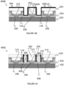
- FIG 4A shows a cross sectional view of a structure 400A that is the structure 300D of Figure 3D that has been processed further in order to provide a replacement LED die 402.
- the replacement LED die 402 (which includes an n-type region, p-type region, active region and p-type contact 414) is contacted with the backplane 202 via the backplane contact 206 of the backplane 200 and the p-type contact 414 of the replacement die LED 402 forming a eutectic bond between the backplane contact 206 and the p-type contact 414.
- the LED die 402 has a conformal layer 404 formed on it in an analogous manner to that of the conformal layer 112 of the monolithically grown structure described with respect to Figures 1 to 3 . Whilst the bond is a eutectic bond, in further examples, alternative and/or additional bonding methods are used to secure the LED die 402 in the structure 400A.
- LED dies may be removed in order to replace dies with different devices.
- red light emitting devices such AlInGaP based red light emitting LED devices
- the method for forming high efficiency red light emitting LEDs differs from that used to form high efficiency blue and/or green light emitting LED devices.
- the number of replacement LED devices that are inserted to provide multi colour light emitting arrays is significantly lower than forming arrays of multi colour light emitting LED devices by pick and place technologies.
- FIG. 4B there is shown a cross sectional view of a structure 400A of Figure 4A that has been processed to provide the structure 400B of Figure 4B .
- the structure 400B includes a metallic conformal layer 406 that has been deposited on the structure 400A. This conformal layer 406 acts to reduce optical crosstalk between pixels associated with light emitting device dies in the display array.
- the process moves to Figure 4C .
- FIG. 4C there is shown a cross sectional view of a structure 400C that is the structure 400D of Figure 4B that has been processed further in order to anisotopically etch the metallic conformal layer 406.
- anisotopically etching results in metal being left on the side walls of the light emitting dies.
- filler material 408 is formed in the gaps between the LED devices.
- Such filler material 408 is deposited using known techniques and planarised using chemical mechanical polishing techniques.
- alternative and/or additional methods are used in order to planarise the n-type side of the device of the structure 400C.
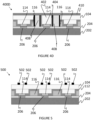
- Figure 4D shows a cross sectional view of a structure 400D that is the structure for 400C of Figure 4C that has been processed in order in order to deposit a transparent conducting material layer 410.
- a transparent conducting material layer 410 is formed from indium tin oxide (ITO).
- ITO indium tin oxide
- FIG. 4D shows a cross sectional view of a structure 400D that is the structure for 400C of Figure 4C that has been processed in order in order to deposit a transparent conducting material layer 410.
- ITO indium tin oxide
- the transparent conducting material layer 410 enables formation of n-type contact with the n-type region 104 of multiple now isolated dies.
- Alternative and/or additional layers are used in further examples, for example metal tracks are used to assist with current spreading.
- a method is described to provide repaired and/or replacement dies in a monolithically grown array of dies, where multiple dies provides a source of light at the light emitting surface associated with a pixel driven by the CMOS backplane 202.
- Figure 5 illustrates how lift-off of selected dies is enhanced.
- Figure 5 shows the structure 500 that is the structure of Figure 3B with additional magnetic material 502 formed in association with individual dies.
- Such magnetic material 502 (for example iron, nickel, cobalt) is deposited on part of the individual LED devices associated with pixels.
- alternative and/or additional configurations are used in order to provide magnetic functionality associated with individual dies.
- the magnetic material 502 is used in order to facilitate lift-off following isolation of pixels. Once repair and/or replacement of defective and/or unrequired dies has been performed, the magnetic material 502 is etched away, enabling the further deposition of transparent conducting material 410 as described with respect to Figure 4D .
- the methods described here enable repair in monolithic micro displays, allowing necessary yield requirements to be achieved. Further, the method enables different colour light emitting LED devices to be deposited on a monolithic display, such as red LED dies into blue/green monolithic displays.
Landscapes
- Led Devices (AREA)
- Devices For Indicating Variable Information By Combining Individual Elements (AREA)
- Led Device Packages (AREA)
- Engineering & Computer Science (AREA)
- Manufacturing & Machinery (AREA)
Claims (12)
- Verfahren zur Bildung einer Anzeige, umfassend:Planarisieren einer Rückplatte (200), die eine Vielzahl elektrischer Kontakte (206) an der Rückplatte umfasst, um eine erste planarisierte Oberfläche bereitzustellen;Planarisieren einer monolithischen lichtemittierenden Diodenstruktur (100), die eine Vielzahl elektrischer Kontakte (114) umfasst, die der Vielzahl elektrischer Kontakte an der Rückplatte entsprechen, um eine zweite planarisierte Oberfläche bereitzustellen;Verbinden der ersten planarisierten Oberfläche mit der zweiten planarisierten Oberfläche, wobei das Verbinden umfasst, eine reversible Verbindung zwischen mindestens einem der Vielzahl elektrischer Kontakte an der Rückplatte und einem entsprechenden elektrischen Kontakt der monolithischen lichtemittierenden Diodenstruktur zu bilden; undanschließend selektives Ätzen der monolithischen lichtemittierenden Diodenstruktur, um eine Vielzahl physisch isolierter lichtemittierender Dioden-Würfel bereitzustellen, wodurch es möglich wird, mindestens einen lichtemittierenden Dioden-Würfel zu entfernen und/oder zu ersetzen, indem die reversible Verbindung zwischen dem mindestens einem der Vielzahl elektrischer Kontakte an der Rückplatte und dem entsprechenden elektrischen Kontakt der monolithischen lichtemittierenden Diodenstruktur rückgängig gemacht wird.
- Verfahren nach Anspruch 1, wobei der mindestens eine der elektrischen Kontakte an der Rückplatte reversibel mit dem entsprechenden elektrischen Kontakt der monolithischen lichtemittierenden Diodenstruktur unter Verwendung einer Metallauf-Metall-Verbindung und/oder eutektischen Verbindung verbunden wird.
- Verfahren nach einem der vorstehenden Ansprüche, umfassend:Entfernen mindestens eines physisch isolierten lichtemittierenden Dioden-Würfels; undErsetzen des mindestens einen physisch isolierten lichtemittierenden Dioden-Würfels durch einen anderen oder mehrere andere lichtemittierende Dioden-Würfel.
- Verfahren nach Anspruch 3, wobei das Entfernen mindestens eines physisch isolierten lichtemittierenden Dioden-Würfels umfasst, die Temperatur der Anzeige zu erhöhen, um so das Entfernen des mindestens einen physisch isolierten lichtemittierenden Dioden-Würfels an der reversiblen Verbindung zwischen dem elektrischen Kontakt an der Rückplatte und dem entsprechenden elektrischen Kontakt, der zur monolithischen lichtemittierenden Diodenstruktur gehört, wobei das Erhöhen der Temperatur der Anzeige bevorzugt umfasst, die Temperatur an der reversiblen Verbindung so zu erhöhen, dass eine eutektische Temperatur der reversiblen Verbindung überschritten wird, wobei die reversible Verbindung bevorzugt mindestens eine von einer eutektischen AuSn-Verbindung, einer eutektischen CuSn-Verbindung und einer eutektischen InSn-Verbindung umfasst.
- Verfahren nach Anspruch 3, wobei das Entfernen mindestens eines physisch isolierten lichtemittierenden Dioden-Würfels umfasst, eine elektrostatische Kraft der reversiblen Verbindung zu überwinden, wobei die elektrostatische Kraft der reversiblen Verbindung bevorzugt die elektrostatische Kraft von mindestens einer von einer Au-Au-Metallverbindung und Cu-Cu-Metallverbindung ist.
- Verfahren nach einem der vorstehenden Ansprüche, umfassend:Testen von mindestens einem der Vielzahl physisch isolierter lichtemittierender Dioden-Würfel;Erkennen eines oder mehrerer defekter lichtemittierender Dioden-Würfel;Entfernen defekter lichtemittierender Dioden-Würfel; undErsetzen des einen oder der mehreren entfernten defekten lichtemittierenden Dioden-Würfel.
- Verfahren nach einem der vorstehenden Ansprüche, umfassend:
Bilden einer oberflächentreuen Metallschicht (406) an mindestens einem Abschnitt der physisch isolierten lichtemittierenden Dioden-Würfel, wodurch sich optisches Übersprechen zwischen physisch isolierten lichtemittierenden Dioden-Würfeln reduziert. - Verfahren nach einem der vorstehenden Ansprüche, umfassend:
Bilden einer transparenten elektrisch leitenden Schicht (410) auf der Vielzahl isolierter lichtemittierender Dioden-Würfel, um auf diese Weise eine herkömmliche Elektrode bereitzustellen. - Verfahren nach einem der vorstehenden Ansprüche, umfassend:
Bilden einer oder mehrere magnetischer Metallregionen (502), die zu mindestens einem der physisch isolierten lichtemittierenden Dioden-Würfel gehört, wodurch das Entfernen physisch isolierter lichtemittierender Dioden-Würfel erleichtert wird. - Verfahren nach einem der vorstehenden Ansprüche, wobei mindestens eine der reversiblen Verbindungen mindestens teilweise seitlich durch eine dielektrische Schicht umgeben wird, wodurch die Rückplatte und die monolithische lichtemittierende Diodenstruktur getrennt werden, wobei die dielektrische Schicht bevorzugt mindestens eins von SiO2, Si3N4, SU-8, SrF2, PDMS und PMMA umfasst.
- Verfahren nach einem der vorstehenden Ansprüche, wobei die Vielzahl der Kontakte der monolithischen lichtemittierenden Diodenstruktur ein hoch reflektierendes Metall umfasst, wobei das hoch reflektierende Metall bevorzugt eins von Ni und Ag ist.
- Verfahren nach einem der vorstehenden Ansprüche, wobei das Entfernen von Material von der monolithischen lichtemittierenden Diodenstruktur umfasst, eine Diskontinuität in mindestens einer Schicht der monolithischen lichtemittierenden Diodenstruktur zu bilden, wobei die mindestens eine Schicht der monolithischen lichtemittierenden Diodenstruktur bevorzugt eine n-Typ-Schicht ist, wobei noch mehr bevorzugt die n-Typ-Schicht eine Schicht aus n-dotiertem Galliumnitrid ist.
Applications Claiming Priority (2)
| Application Number | Priority Date | Filing Date | Title |
|---|---|---|---|
| GB2009890.1A GB2596533B (en) | 2020-06-29 | 2020-06-29 | Hybrid microdisplay |
| PCT/GB2021/051573 WO2022003323A1 (en) | 2020-06-29 | 2021-06-22 | Method of forming a display and display |
Publications (2)
| Publication Number | Publication Date |
|---|---|
| EP4173046A1 EP4173046A1 (de) | 2023-05-03 |
| EP4173046B1 true EP4173046B1 (de) | 2025-01-15 |
Family
ID=71949625
Family Applications (1)
| Application Number | Title | Priority Date | Filing Date |
|---|---|---|---|
| EP21737742.3A Active EP4173046B1 (de) | 2020-06-29 | 2021-06-22 | Verfahren zur bildung einer anzeige |
Country Status (8)
| Country | Link |
|---|---|
| US (1) | US12604583B2 (de) |
| EP (1) | EP4173046B1 (de) |
| JP (1) | JP7768912B2 (de) |
| KR (1) | KR102841839B1 (de) |
| CN (1) | CN115943496A (de) |
| GB (1) | GB2596533B (de) |
| TW (1) | TWI858270B (de) |
| WO (1) | WO2022003323A1 (de) |
Families Citing this family (5)
| Publication number | Priority date | Publication date | Assignee | Title |
|---|---|---|---|---|
| TWI808422B (zh) | 2021-05-21 | 2023-07-11 | 錼創顯示科技股份有限公司 | 接著層結構以及半導體結構 |
| CN113299593B (zh) * | 2021-05-21 | 2023-01-10 | 錼创显示科技股份有限公司 | 接着层结构以及半导体结构 |
| WO2024193934A1 (en) * | 2023-03-23 | 2024-09-26 | Ams-Osram International Gmbh | Method for producing optoelectronic semiconductor chips and optoelectronic semiconductor chip |
| WO2025091226A1 (en) * | 2023-10-31 | 2025-05-08 | Jade Bird Display (shanghai) Limited | Micro-led array layer and micro-led display panel |
| WO2025239839A1 (en) * | 2024-05-17 | 2025-11-20 | New Silicon Corporation Pte Ltd | Pixel chip, display panel, method of fabricating a pixel chip |
Citations (1)
| Publication number | Priority date | Publication date | Assignee | Title |
|---|---|---|---|---|
| WO2019079381A1 (en) * | 2017-10-19 | 2019-04-25 | Spy Eye, Llc | ULTRA-DENSE LED PROJECTOR |
Family Cites Families (20)
| Publication number | Priority date | Publication date | Assignee | Title |
|---|---|---|---|---|
| CN101005110A (zh) * | 2007-01-12 | 2007-07-25 | 中国科学院上海微系统与信息技术研究所 | 采用金属键合工艺实现氮化镓发光二极管垂直结构的方法 |
| US8573469B2 (en) * | 2011-11-18 | 2013-11-05 | LuxVue Technology Corporation | Method of forming a micro LED structure and array of micro LED structures with an electrically insulating layer |
| KR20130092896A (ko) | 2012-02-13 | 2013-08-21 | 엘지전자 주식회사 | Led 디스플레이 장치 및 그것의 제조 방법 |
| FR3028672B1 (fr) | 2014-11-18 | 2018-01-26 | Commissariat A L'energie Atomique Et Aux Energies Alternatives | Dispositif optoelectronique a diodes electroluminescentes |
| CN105789122B (zh) | 2014-12-12 | 2019-05-03 | 财团法人工业技术研究院 | 光电元件的转移方法 |
| FR3033939B1 (fr) | 2015-03-20 | 2018-04-27 | Commissariat A L'energie Atomique Et Aux Energies Alternatives | Dispositif optoelectronique a diode electroluminescente |
| WO2016188505A1 (en) * | 2015-05-22 | 2016-12-01 | Hiphoton Co., Ltd | Structure of a semiconductor array |
| EP3455882B1 (de) | 2016-05-13 | 2021-08-11 | Commissariat à l'Energie Atomique et aux Energies Alternatives | Verfahren zur herstellung einer optoelektronischen vorrichtung mit mehreren galliumnitriddioden |
| US10361341B2 (en) | 2016-10-24 | 2019-07-23 | Glo Ab | Indium gallium nitride red light emitting diode and method of making thereof |
| US10902770B2 (en) * | 2016-12-22 | 2021-01-26 | Sharp Kabushiki Kaisha | Display device |
| JP6366799B1 (ja) * | 2017-02-10 | 2018-08-01 | ルーメンス カンパニー リミテッド | マイクロledモジュール及びその製造方法 |
| CN110462850B (zh) | 2017-03-20 | 2024-04-16 | 上海显耀显示科技有限公司 | 通过堆叠微型led的层来制造半导体器件 |
| JP6936867B2 (ja) | 2017-11-10 | 2021-09-22 | シャープ株式会社 | 半導体モジュール、表示装置、及び半導体モジュールの製造方法 |
| JP7140315B2 (ja) * | 2018-03-14 | 2022-09-21 | 京東方科技集團股▲ふん▼有限公司 | 複数のマイクロ発光ダイオードをターゲット基板に転写する方法 |
| FR3079350B1 (fr) * | 2018-03-22 | 2020-03-27 | Commissariat A L'energie Atomique Et Aux Energies Alternatives | Dispositif d'affichage emissif a led et procede de fabrication d'un tel dispositif |
| KR20190114333A (ko) * | 2018-03-29 | 2019-10-10 | (주)포인트엔지니어링 | 마이크로 led의 검사방법 |
| CN110504346B (zh) * | 2018-05-16 | 2021-06-25 | 鸿富锦精密工业(深圳)有限公司 | 微型led显示面板制作方法及显示面板 |
| US10985046B2 (en) * | 2018-06-22 | 2021-04-20 | Veeco Instruments Inc. | Micro-LED transfer methods using light-based debonding |
| JP7146595B2 (ja) * | 2018-11-27 | 2022-10-04 | 株式会社ジャパンディスプレイ | 表示パネル、表示パネルの製造方法、及び基板 |
| US10903267B2 (en) * | 2019-04-04 | 2021-01-26 | Bor-Jen Wu | System and method for making micro LED display |
-
2020
- 2020-06-29 GB GB2009890.1A patent/GB2596533B/en active Active
-
2021
- 2021-06-22 CN CN202180045289.7A patent/CN115943496A/zh active Pending
- 2021-06-22 JP JP2022580838A patent/JP7768912B2/ja active Active
- 2021-06-22 US US17/924,846 patent/US12604583B2/en active Active
- 2021-06-22 WO PCT/GB2021/051573 patent/WO2022003323A1/en not_active Ceased
- 2021-06-22 EP EP21737742.3A patent/EP4173046B1/de active Active
- 2021-06-22 KR KR1020227044541A patent/KR102841839B1/ko active Active
- 2021-06-29 TW TW110123891A patent/TWI858270B/zh active
Patent Citations (1)
| Publication number | Priority date | Publication date | Assignee | Title |
|---|---|---|---|---|
| WO2019079381A1 (en) * | 2017-10-19 | 2019-04-25 | Spy Eye, Llc | ULTRA-DENSE LED PROJECTOR |
Also Published As
| Publication number | Publication date |
|---|---|
| JP2023532906A (ja) | 2023-08-01 |
| WO2022003323A1 (en) | 2022-01-06 |
| TWI858270B (zh) | 2024-10-11 |
| GB2596533B (en) | 2023-02-15 |
| JP7768912B2 (ja) | 2025-11-12 |
| US12604583B2 (en) | 2026-04-14 |
| CN115943496A (zh) | 2023-04-07 |
| TW202205712A (zh) | 2022-02-01 |
| EP4173046A1 (de) | 2023-05-03 |
| US20230187592A1 (en) | 2023-06-15 |
| KR102841839B1 (ko) | 2025-08-04 |
| GB202009890D0 (en) | 2020-08-12 |
| KR20230029648A (ko) | 2023-03-03 |
| GB2596533A (en) | 2022-01-05 |
Similar Documents
| Publication | Publication Date | Title |
|---|---|---|
| US12604583B2 (en) | Hybrid microdisplay | |
| US11715730B2 (en) | Direct-bonded LED arrays including optical elements configured to transmit optical signals from LED elements | |
| CN114188459B (zh) | 微型发光二极管显示装置及其制作方法 | |
| KR102814860B1 (ko) | 발광 어레이 | |
| CN115176347B (zh) | 高分辨率单体式rgb阵列 | |
| CN114759130B (zh) | 一种Micro-LED显示芯片及其制备方法 | |
| US12040344B2 (en) | Light emitting device and display apparatus having the same | |
| KR20250099328A (ko) | 다중컬러 발광 마이크로 led 디스플레이 및 그 제조 방법 | |
| KR102832422B1 (ko) | 모놀리식 전자 디바이스 | |
| US20240313182A1 (en) | Light emitting device and display apparatus having the same | |
| WO2024119056A1 (en) | Display including lateral-structure multicolor light emitting device pixels and method of fabrication thereof | |
| US12615899B2 (en) | Light emitting device and display apparatus having the same | |
| KR102721221B1 (ko) | 반도체 소자용 템플릿을 이용한 반도체 적층체 및 그 제조 방법 | |
| CN115458663B (zh) | 一种全彩化倒装发光二极管芯片单元、制备方法及显示屏 | |
| US20230223494A1 (en) | Light emitting diodes and method of making thereof by selectively growing active layers from trench separated areas | |
| EP4250378B1 (de) | Verfahren zur herstellung von lichtemittierenden elementen mit resonanzhohlraum und optische vorrichtung mit diesen elementen | |
| KR20260007646A (ko) | 표시 장치 및 표시 장치의 제조 방법 |
Legal Events
| Date | Code | Title | Description |
|---|---|---|---|
| STAA | Information on the status of an ep patent application or granted ep patent |
Free format text: STATUS: UNKNOWN |
|
| STAA | Information on the status of an ep patent application or granted ep patent |
Free format text: STATUS: THE INTERNATIONAL PUBLICATION HAS BEEN MADE |
|
| PUAI | Public reference made under article 153(3) epc to a published international application that has entered the european phase |
Free format text: ORIGINAL CODE: 0009012 |
|
| STAA | Information on the status of an ep patent application or granted ep patent |
Free format text: STATUS: REQUEST FOR EXAMINATION WAS MADE |
|
| 17P | Request for examination filed |
Effective date: 20221025 |
|
| AK | Designated contracting states |
Kind code of ref document: A1 Designated state(s): AL AT BE BG CH CY CZ DE DK EE ES FI FR GB GR HR HU IE IS IT LI LT LU LV MC MK MT NL NO PL PT RO RS SE SI SK SM TR |
|
| DAV | Request for validation of the european patent (deleted) | ||
| DAX | Request for extension of the european patent (deleted) | ||
| GRAP | Despatch of communication of intention to grant a patent |
Free format text: ORIGINAL CODE: EPIDOSNIGR1 |
|
| STAA | Information on the status of an ep patent application or granted ep patent |
Free format text: STATUS: GRANT OF PATENT IS INTENDED |
|
| INTG | Intention to grant announced |
Effective date: 20240916 |
|
| P01 | Opt-out of the competence of the unified patent court (upc) registered |
Free format text: CASE NUMBER: APP_58126/2024 Effective date: 20241024 |
|
| GRAS | Grant fee paid |
Free format text: ORIGINAL CODE: EPIDOSNIGR3 |
|
| GRAA | (expected) grant |
Free format text: ORIGINAL CODE: 0009210 |
|
| STAA | Information on the status of an ep patent application or granted ep patent |
Free format text: STATUS: THE PATENT HAS BEEN GRANTED |
|
| RBV | Designated contracting states (corrected) |
Designated state(s): AL AT BE BG CH CY CZ DE DK EE ES FI FR GR HR HU IE IS IT LI LT LU LV MC MK MT NL NO PL PT RO RS SE SI SK SM TR |
|
| AK | Designated contracting states |
Kind code of ref document: B1 Designated state(s): AL AT BE BG CH CY CZ DE DK EE ES FI FR GR HR HU IE IS IT LI LT LU LV MC MK MT NL NO PL PT RO RS SE SI SK SM TR |
|
| REG | Reference to a national code |
Ref country code: CH Ref legal event code: EP |
|
| REG | Reference to a national code |
Ref country code: DE Ref legal event code: R096 Ref document number: 602021024994 Country of ref document: DE |
|
| REG | Reference to a national code |
Ref country code: IE Ref legal event code: FG4D |
|
| REG | Reference to a national code |
Ref country code: NL Ref legal event code: MP Effective date: 20250115 |
|
| PG25 | Lapsed in a contracting state [announced via postgrant information from national office to epo] |
Ref country code: NL Free format text: LAPSE BECAUSE OF FAILURE TO SUBMIT A TRANSLATION OF THE DESCRIPTION OR TO PAY THE FEE WITHIN THE PRESCRIBED TIME-LIMIT Effective date: 20250115 |
|
| PG25 | Lapsed in a contracting state [announced via postgrant information from national office to epo] |
Ref country code: RS Free format text: LAPSE BECAUSE OF FAILURE TO SUBMIT A TRANSLATION OF THE DESCRIPTION OR TO PAY THE FEE WITHIN THE PRESCRIBED TIME-LIMIT Effective date: 20250415 |
|
| PG25 | Lapsed in a contracting state [announced via postgrant information from national office to epo] |
Ref country code: FI Free format text: LAPSE BECAUSE OF FAILURE TO SUBMIT A TRANSLATION OF THE DESCRIPTION OR TO PAY THE FEE WITHIN THE PRESCRIBED TIME-LIMIT Effective date: 20250115 |
|
| PG25 | Lapsed in a contracting state [announced via postgrant information from national office to epo] |
Ref country code: PL Free format text: LAPSE BECAUSE OF FAILURE TO SUBMIT A TRANSLATION OF THE DESCRIPTION OR TO PAY THE FEE WITHIN THE PRESCRIBED TIME-LIMIT Effective date: 20250115 |
|
| PGFP | Annual fee paid to national office [announced via postgrant information from national office to epo] |
Ref country code: DE Payment date: 20250618 Year of fee payment: 5 |
|
| PG25 | Lapsed in a contracting state [announced via postgrant information from national office to epo] |
Ref country code: ES Free format text: LAPSE BECAUSE OF FAILURE TO SUBMIT A TRANSLATION OF THE DESCRIPTION OR TO PAY THE FEE WITHIN THE PRESCRIBED TIME-LIMIT Effective date: 20250115 |
|
| REG | Reference to a national code |
Ref country code: LT Ref legal event code: MG9D |
|
| PG25 | Lapsed in a contracting state [announced via postgrant information from national office to epo] |
Ref country code: NO Free format text: LAPSE BECAUSE OF FAILURE TO SUBMIT A TRANSLATION OF THE DESCRIPTION OR TO PAY THE FEE WITHIN THE PRESCRIBED TIME-LIMIT Effective date: 20250415 Ref country code: IS Free format text: LAPSE BECAUSE OF FAILURE TO SUBMIT A TRANSLATION OF THE DESCRIPTION OR TO PAY THE FEE WITHIN THE PRESCRIBED TIME-LIMIT Effective date: 20250515 |
|
| REG | Reference to a national code |
Ref country code: AT Ref legal event code: MK05 Ref document number: 1760418 Country of ref document: AT Kind code of ref document: T Effective date: 20250115 |
|
| PG25 | Lapsed in a contracting state [announced via postgrant information from national office to epo] |
Ref country code: HR Free format text: LAPSE BECAUSE OF FAILURE TO SUBMIT A TRANSLATION OF THE DESCRIPTION OR TO PAY THE FEE WITHIN THE PRESCRIBED TIME-LIMIT Effective date: 20250115 |
|
| PG25 | Lapsed in a contracting state [announced via postgrant information from national office to epo] |
Ref country code: PT Free format text: LAPSE BECAUSE OF FAILURE TO SUBMIT A TRANSLATION OF THE DESCRIPTION OR TO PAY THE FEE WITHIN THE PRESCRIBED TIME-LIMIT Effective date: 20250515 Ref country code: LV Free format text: LAPSE BECAUSE OF FAILURE TO SUBMIT A TRANSLATION OF THE DESCRIPTION OR TO PAY THE FEE WITHIN THE PRESCRIBED TIME-LIMIT Effective date: 20250115 |
|
| PGFP | Annual fee paid to national office [announced via postgrant information from national office to epo] |
Ref country code: FR Payment date: 20250627 Year of fee payment: 5 |
|
| PG25 | Lapsed in a contracting state [announced via postgrant information from national office to epo] |
Ref country code: BG Free format text: LAPSE BECAUSE OF FAILURE TO SUBMIT A TRANSLATION OF THE DESCRIPTION OR TO PAY THE FEE WITHIN THE PRESCRIBED TIME-LIMIT Effective date: 20250115 Ref country code: GR Free format text: LAPSE BECAUSE OF FAILURE TO SUBMIT A TRANSLATION OF THE DESCRIPTION OR TO PAY THE FEE WITHIN THE PRESCRIBED TIME-LIMIT Effective date: 20250416 |
|
| PG25 | Lapsed in a contracting state [announced via postgrant information from national office to epo] |
Ref country code: AT Free format text: LAPSE BECAUSE OF FAILURE TO SUBMIT A TRANSLATION OF THE DESCRIPTION OR TO PAY THE FEE WITHIN THE PRESCRIBED TIME-LIMIT Effective date: 20250115 |
|
| PGFP | Annual fee paid to national office [announced via postgrant information from national office to epo] |
Ref country code: IE Payment date: 20250618 Year of fee payment: 5 |
|
| PG25 | Lapsed in a contracting state [announced via postgrant information from national office to epo] |
Ref country code: SE Free format text: LAPSE BECAUSE OF FAILURE TO SUBMIT A TRANSLATION OF THE DESCRIPTION OR TO PAY THE FEE WITHIN THE PRESCRIBED TIME-LIMIT Effective date: 20250115 |
|
| PG25 | Lapsed in a contracting state [announced via postgrant information from national office to epo] |
Ref country code: SM Free format text: LAPSE BECAUSE OF FAILURE TO SUBMIT A TRANSLATION OF THE DESCRIPTION OR TO PAY THE FEE WITHIN THE PRESCRIBED TIME-LIMIT Effective date: 20250115 |
|
| PG25 | Lapsed in a contracting state [announced via postgrant information from national office to epo] |
Ref country code: DK Free format text: LAPSE BECAUSE OF FAILURE TO SUBMIT A TRANSLATION OF THE DESCRIPTION OR TO PAY THE FEE WITHIN THE PRESCRIBED TIME-LIMIT Effective date: 20250115 |
|
| PGFP | Annual fee paid to national office [announced via postgrant information from national office to epo] |
Ref country code: IT Payment date: 20250619 Year of fee payment: 5 |
|
| REG | Reference to a national code |
Ref country code: DE Ref legal event code: R097 Ref document number: 602021024994 Country of ref document: DE |
|
| PG25 | Lapsed in a contracting state [announced via postgrant information from national office to epo] |
Ref country code: EE Free format text: LAPSE BECAUSE OF FAILURE TO SUBMIT A TRANSLATION OF THE DESCRIPTION OR TO PAY THE FEE WITHIN THE PRESCRIBED TIME-LIMIT Effective date: 20250115 Ref country code: CZ Free format text: LAPSE BECAUSE OF FAILURE TO SUBMIT A TRANSLATION OF THE DESCRIPTION OR TO PAY THE FEE WITHIN THE PRESCRIBED TIME-LIMIT Effective date: 20250115 |
|
| PG25 | Lapsed in a contracting state [announced via postgrant information from national office to epo] |
Ref country code: RO Free format text: LAPSE BECAUSE OF FAILURE TO SUBMIT A TRANSLATION OF THE DESCRIPTION OR TO PAY THE FEE WITHIN THE PRESCRIBED TIME-LIMIT Effective date: 20250115 |
|
| PG25 | Lapsed in a contracting state [announced via postgrant information from national office to epo] |
Ref country code: SK Free format text: LAPSE BECAUSE OF FAILURE TO SUBMIT A TRANSLATION OF THE DESCRIPTION OR TO PAY THE FEE WITHIN THE PRESCRIBED TIME-LIMIT Effective date: 20250115 |
|
| PLBE | No opposition filed within time limit |
Free format text: ORIGINAL CODE: 0009261 |
|
| STAA | Information on the status of an ep patent application or granted ep patent |
Free format text: STATUS: NO OPPOSITION FILED WITHIN TIME LIMIT |
|
| REG | Reference to a national code |
Ref country code: CH Ref legal event code: L10 Free format text: ST27 STATUS EVENT CODE: U-0-0-L10-L00 (AS PROVIDED BY THE NATIONAL OFFICE) Effective date: 20251126 |
|
| 26N | No opposition filed |
Effective date: 20251016 |
|
| REG | Reference to a national code |
Ref country code: CH Ref legal event code: H13 Free format text: ST27 STATUS EVENT CODE: U-0-0-H10-H13 (AS PROVIDED BY THE NATIONAL OFFICE) Effective date: 20260127 |
|
| PG25 | Lapsed in a contracting state [announced via postgrant information from national office to epo] |
Ref country code: MC Free format text: LAPSE BECAUSE OF FAILURE TO SUBMIT A TRANSLATION OF THE DESCRIPTION OR TO PAY THE FEE WITHIN THE PRESCRIBED TIME-LIMIT Effective date: 20250115 |
|
| PG25 | Lapsed in a contracting state [announced via postgrant information from national office to epo] |
Ref country code: LU Free format text: LAPSE BECAUSE OF NON-PAYMENT OF DUE FEES Effective date: 20250622 |
|
| REG | Reference to a national code |
Ref country code: BE Ref legal event code: MM Effective date: 20250630 |
|
| PG25 | Lapsed in a contracting state [announced via postgrant information from national office to epo] |
Ref country code: BE Free format text: LAPSE BECAUSE OF NON-PAYMENT OF DUE FEES Effective date: 20250630 |
|
| PG25 | Lapsed in a contracting state [announced via postgrant information from national office to epo] |
Ref country code: CH Free format text: LAPSE BECAUSE OF NON-PAYMENT OF DUE FEES Effective date: 20250630 |