EP4173046B1 - Method of forming a display - Google Patents
Method of forming a display Download PDFInfo
- Publication number
- EP4173046B1 EP4173046B1 EP21737742.3A EP21737742A EP4173046B1 EP 4173046 B1 EP4173046 B1 EP 4173046B1 EP 21737742 A EP21737742 A EP 21737742A EP 4173046 B1 EP4173046 B1 EP 4173046B1
- Authority
- EP
- European Patent Office
- Prior art keywords
- light emitting
- emitting diode
- dies
- backplane
- bond
- Prior art date
- Legal status (The legal status is an assumption and is not a legal conclusion. Google has not performed a legal analysis and makes no representation as to the accuracy of the status listed.)
- Active
Links
Images

Classifications
-
- H—ELECTRICITY
- H10—SEMICONDUCTOR DEVICES; ELECTRIC SOLID-STATE DEVICES NOT OTHERWISE PROVIDED FOR
- H10H—INORGANIC LIGHT-EMITTING SEMICONDUCTOR DEVICES HAVING POTENTIAL BARRIERS
- H10H20/00—Individual inorganic light-emitting semiconductor devices having potential barriers, e.g. light-emitting diodes [LED]
- H10H20/01—Manufacture or treatment
-
- H—ELECTRICITY
- H10—SEMICONDUCTOR DEVICES; ELECTRIC SOLID-STATE DEVICES NOT OTHERWISE PROVIDED FOR
- H10H—INORGANIC LIGHT-EMITTING SEMICONDUCTOR DEVICES HAVING POTENTIAL BARRIERS
- H10H20/00—Individual inorganic light-emitting semiconductor devices having potential barriers, e.g. light-emitting diodes [LED]
- H10H20/01—Manufacture or treatment
- H10H20/011—Manufacture or treatment of bodies, e.g. forming semiconductor layers
- H10H20/013—Manufacture or treatment of bodies, e.g. forming semiconductor layers having light-emitting regions comprising only Group III-V materials
- H10H20/0137—Manufacture or treatment of bodies, e.g. forming semiconductor layers having light-emitting regions comprising only Group III-V materials the light-emitting regions comprising nitride materials
-
- H—ELECTRICITY
- H10—SEMICONDUCTOR DEVICES; ELECTRIC SOLID-STATE DEVICES NOT OTHERWISE PROVIDED FOR
- H10H—INORGANIC LIGHT-EMITTING SEMICONDUCTOR DEVICES HAVING POTENTIAL BARRIERS
- H10H20/00—Individual inorganic light-emitting semiconductor devices having potential barriers, e.g. light-emitting diodes [LED]
- H10H20/01—Manufacture or treatment
- H10H20/011—Manufacture or treatment of bodies, e.g. forming semiconductor layers
- H10H20/018—Bonding of wafers
-
- H—ELECTRICITY
- H10—SEMICONDUCTOR DEVICES; ELECTRIC SOLID-STATE DEVICES NOT OTHERWISE PROVIDED FOR
- H10H—INORGANIC LIGHT-EMITTING SEMICONDUCTOR DEVICES HAVING POTENTIAL BARRIERS
- H10H20/00—Individual inorganic light-emitting semiconductor devices having potential barriers, e.g. light-emitting diodes [LED]
- H10H20/01—Manufacture or treatment
- H10H20/036—Manufacture or treatment of packages
- H10H20/0364—Manufacture or treatment of packages of interconnections
-
- H—ELECTRICITY
- H10—SEMICONDUCTOR DEVICES; ELECTRIC SOLID-STATE DEVICES NOT OTHERWISE PROVIDED FOR
- H10H—INORGANIC LIGHT-EMITTING SEMICONDUCTOR DEVICES HAVING POTENTIAL BARRIERS
- H10H20/00—Individual inorganic light-emitting semiconductor devices having potential barriers, e.g. light-emitting diodes [LED]
- H10H20/80—Constructional details
- H10H20/81—Bodies
-
- H—ELECTRICITY
- H10—SEMICONDUCTOR DEVICES; ELECTRIC SOLID-STATE DEVICES NOT OTHERWISE PROVIDED FOR
- H10H—INORGANIC LIGHT-EMITTING SEMICONDUCTOR DEVICES HAVING POTENTIAL BARRIERS
- H10H20/00—Individual inorganic light-emitting semiconductor devices having potential barriers, e.g. light-emitting diodes [LED]
- H10H20/80—Constructional details
- H10H20/83—Electrodes
- H10H20/832—Electrodes characterised by their material
- H10H20/833—Transparent materials
-
- H—ELECTRICITY
- H10—SEMICONDUCTOR DEVICES; ELECTRIC SOLID-STATE DEVICES NOT OTHERWISE PROVIDED FOR
- H10H—INORGANIC LIGHT-EMITTING SEMICONDUCTOR DEVICES HAVING POTENTIAL BARRIERS
- H10H20/00—Individual inorganic light-emitting semiconductor devices having potential barriers, e.g. light-emitting diodes [LED]
- H10H20/80—Constructional details
- H10H20/83—Electrodes
- H10H20/832—Electrodes characterised by their material
- H10H20/835—Reflective materials
-
- H—ELECTRICITY
- H10—SEMICONDUCTOR DEVICES; ELECTRIC SOLID-STATE DEVICES NOT OTHERWISE PROVIDED FOR
- H10H—INORGANIC LIGHT-EMITTING SEMICONDUCTOR DEVICES HAVING POTENTIAL BARRIERS
- H10H29/00—Integrated devices, or assemblies of multiple devices, comprising at least one light-emitting semiconductor element covered by group H10H20/00
- H10H29/10—Integrated devices comprising at least one light-emitting semiconductor component covered by group H10H20/00
- H10H29/14—Integrated devices comprising at least one light-emitting semiconductor component covered by group H10H20/00 comprising multiple light-emitting semiconductor components
- H10H29/142—Two-dimensional arrangements, e.g. asymmetric LED layout
-
- H—ELECTRICITY
- H10—SEMICONDUCTOR DEVICES; ELECTRIC SOLID-STATE DEVICES NOT OTHERWISE PROVIDED FOR
- H10W—GENERIC PACKAGES, INTERCONNECTIONS, CONNECTORS OR OTHER CONSTRUCTIONAL DETAILS OF DEVICES COVERED BY CLASS H10
- H10W90/00—Package configurations
-
- H—ELECTRICITY
- H10—SEMICONDUCTOR DEVICES; ELECTRIC SOLID-STATE DEVICES NOT OTHERWISE PROVIDED FOR
- H10H—INORGANIC LIGHT-EMITTING SEMICONDUCTOR DEVICES HAVING POTENTIAL BARRIERS
- H10H20/00—Individual inorganic light-emitting semiconductor devices having potential barriers, e.g. light-emitting diodes [LED]
- H10H20/80—Constructional details
- H10H20/84—Coatings, e.g. passivation layers or antireflective coatings
-
- H—ELECTRICITY
- H10—SEMICONDUCTOR DEVICES; ELECTRIC SOLID-STATE DEVICES NOT OTHERWISE PROVIDED FOR
- H10H—INORGANIC LIGHT-EMITTING SEMICONDUCTOR DEVICES HAVING POTENTIAL BARRIERS
- H10H20/00—Individual inorganic light-emitting semiconductor devices having potential barriers, e.g. light-emitting diodes [LED]
- H10H20/80—Constructional details
- H10H20/85—Packages
- H10H20/857—Interconnections, e.g. lead-frames, bond wires or solder balls
Definitions
- the invention relates to the formation of a display.
- the invention relates to a method of forming a monolithic-based micro LED display with the facility to replace pixels.
- LED devices Light emitting diode (LED) devices are known to provide highly efficient and controllable light sources for display applications.
- LED devices are known to provide highly efficient and controllable light sources for display applications.
- the implementation of LED devices into micro LED arrays with small pixels at an ultra-fine pitch enables the production of high resolution displays.
- the presence of any defective LED devices in such arrays can be problematic.
- the number of dead pixels e.g., defective LED devices in a micro LED array
- the number of dead pixels is preferably less than 2 dead pixels per 2 million pixels (i.e., a successful yield of 99.9999%) in order to provide an acceptable display.
- redundancy schemes are known to be implemented, where back-up devices are provided in an LED array in order to provide light to pixels where there is a failure of any device.
- redundancy schemes use additional space, which affects the provision of closely packed, small, LED devices (dies) and hence pixels in micro LED displays.
- Document WO 2019/079381 A1 discloses a monolithic ultra-dense light emitting diode display having a dielectric material that insulates sidewalls of a P-type layer and an active layer from a reflective metal, and electrically contacts an N-type layer of a pillar, and further discloses a method of forming said display.
- a display comprising: a backplane comprising a plurality of backplane electrical contacts bonded to a plurality of physically isolated light emitting diode dies having an electrical contact, wherein at least one of the plurality of backplane electrical contacts is bonded to a corresponding electrical contact of the plurality of physically isolated light emitting diode dies using a reversible bond, thereby to enable removal and/or replacement of at least one physically isolated light emitting diode die by reversing the reversible bond between the at least one backplane electrical contact and the corresponding electrical contact of the plurality of physically isolated light emitting diode dies, wherein the plurality of physically isolated light emitting diode dies are formed from a monolithic light emitting diode structure.
- the formation of a display by bonding a backplane to a monolithic light emitting diode structure, removing material and forming reversible bonds between at least one of a plurality of backplane electrical contacts and the corresponding electrical contact of the monolithic light emitting diode structure means that individual LED dies can be identified and replaced, thereby ensuring that a sufficiently high yield of functional devices is present in a display without requiring space to be used for redundancy.
- arrays of light emitting pixels can be provided in a high resolution display with the facility to replace individual light emitting diode device dies, where required.
- the at least one of the backplane electrical contacts is reversibly bonded to the corresponding electrical contact of the monolithic light emitting diode structure using metal-to-metal bonding and/or eutectic bonding.
- bonding facilitates removal and replacement of LED devices whilst providing the electrical conductivity to form functioning devices and whilst providing a reflective surface to aid light extraction from individual LED devices.
- the method comprises: removing at least one physically isolated light emitting diode die; and replacing the at least one physically isolated light emitting diode die with a different one or more light emitting diode dies.
- the display is adapted to provide light emission from individual light emitting devices in an array with a preferred arrangement of light emission properties.
- the method comprises: removing at least one physically isolated light emitting diode die comprises increasing the temperature of the display thereby to enable removal of the at least one physically isolated light emitting diode die at the reversible bond between the backplane electrical contact and the corresponding electrical contact associated with the monolithic light emitting diode structure, preferably wherein increasing the temperature of the display comprises increasing the temperature at the reversible bond to surpass a eutectic temperature of the reversible bond, preferably wherein the reversible bond comprises at least one of a AuSn eutectic bond, a CuSn eutectic bond and a InSn eutectic bond.
- a controllable method is presented that simultaneously enables electrical conductivity, reversible bonding and relatively high reflectivity for enhanced light extraction.
- removing at least one physically isolated light emitting diode die comprises overcoming an electrostatic force of the reversible bond, preferably wherein the electrostatic force of the reversible bond is the electrostatic force of at least one of a Au-Au metal bond and a Cu-Cu metal bond.
- metal-metal bonds can be provided that simultaneously enable electrical conductivity, reversible bonding and relatively high reflectivity for enhanced light extraction.
- the method comprises: testing at least one of the plurality of physically isolated light emitting diode dies; identifying one or more defective light emitting diode dies; removing defective light emitting diode dies; and replacing the one or more removed light emitting diode dies.
- displays with high yields of working devices are provided based on monolithically grown LED devices, thereby providing high resolution displays.
- the method comprises: forming a conformal metal layer on at least a portion of the physically isolated light emitting diode dies, thereby to reduce optical cross talk between physically isolated light emitting diode dies.
- a conformal metal layer on at least a portion of the physically isolated light emitting diode dies, thereby to reduce optical cross talk between physically isolated light emitting diode dies.
- light extraction from individual LED dies is enhanced and the contrast between pixels associated with LED dies is improved.
- the method comprises: forming a transparent electrically conductive layer on the plurality of isolated light emitting diode dies, thereby to provide a common electrode.
- a transparent electrically conductive layer on the plurality of isolated light emitting diode dies, thereby to provide a common electrode.
- multiple devices in an array are simultaneously contacted thereby efficiently processing large numbers of devices.
- the method comprises: forming one or more magnetic metal regions associated with at least one of the physically isolated light emitting diode dies, thereby to facilitate removal of physically isolated light emitting diode dies.
- removal of individually dies is enhanced by the use of magnetic materials, thereby overcoming any residual forces to aid removal of individual LED devices.
- At least one of the reversible bonds is at least partially laterally surrounded by a dielectric layer thereby to separate the backplane and the monolithic light emitting diode structure, preferably wherein the dielectric layer comprises at least one of SiO 2 , Si 3 N 4 , Su-8, SrF 2 , PDMS and PMMA.
- the dielectric layer enables uniform processing without preventing removal of individual LED dies.
- the plurality of contacts of the monolithic light emitting structure comprises a high reflectivity metal, preferably wherein the high reflectivity metal is one of nickel (Ni) and silver (Ag).
- the high reflectivity metal is one of nickel (Ni) and silver (Ag).
- Ni nickel
- Ag silver
- such metal simultaneously provides electric conductivity whilst aiding light extraction.
- removing material from the monolithic light emitting diode structure comprises forming a discontinuity in at least one layer of the monolithic light emitting diode structure, preferably wherein the at least one layer of the monolithic light emitting diode structure is an n-type layer, more preferably wherein the n-type layer is an n-doped gallium nitride layer.
- forming discontinuities enables removal and replacement of individual, physically isolated dies.
- the method and structure enables display arrays of pixels to be provided, where the e.g., where the light emitting surface area of each pixel is less than or equal to 100 ⁇ m 2 , and preferably less than or equal to 16 ⁇ m 2 , and where the pixel pitch is less than 10 ⁇ m and preferably less than 4 ⁇ m and more preferably less than 3 ⁇ m.
- the method and structure described here is used to replace defective dies, in further examples it is used to provide LED dies in the array that are configured to emit light of a different wavelength to the dies formed in the monolithically grown array of LED devices.
- LED dies in the array that are configured to emit light of a different wavelength to the dies formed in the monolithically grown array of LED devices.
- Gallium arsenide (GaAs) based materials are a more established technology for red-light emitting LED dies. Therefore, in an example, the method described herein is used to replace LED dies in monolithically grown arrays of nitride-based LED dies to provide light of different wavelengths.
- the number of dies that would be transferred into the monolithically grown array is much less than the total number of dies in the array, providing a more efficient and practical
- Figure 1A a cross sectional view of an epitaxial crystalline structure 100A.
- the epitaxial crystalline structure 100A is a structure formed from crystalline layers sequentially grown or deposited to provide a light emitting structure.
- the epitaxial crystalline structure 100A is provided using metal organic chemical vapour deposition (MOCVD).
- MOCVD metal organic chemical vapour deposition
- alternative and/or additional methods of growth and/or deposition are used to provide the epitaxial crystalline structure 100A, for example molecular beam epitaxy (MBE).
- MBE molecular beam epitaxy
- the epitaxial crystalline structure 100A is provided in a continuous growth process and has a high crystalline quality and low defect density.
- the epitaxial structure 100A is provided using multiple growth steps that enable the selective provision of particular qualities, for example different wavelengths of light emission upon radiative recombination of carriers from different areas of the epitaxial crystalline structure 100A.
- a growth substrate 102 upon which there is grown an n-type region 104.
- the growth substrate 102 is a silicon substrate. Alternatively, in further examples different material is used in order to provide a growth substrate 102.
- the n-type region 104 is formed from n-type doped gallium nitride (GaN). In further examples, the n-type region 104 is formed from additional and/or alternative layers. For example, further buffer layers are included.
- an active region 106 On top of the n-type region 104 there is shown an active region 106.
- the active region 106 is configured to emit light following the recombination of carriers injected from n-type and p-type regions.
- the active region 106 includes a multiple quantum well (MQW) structure.
- MQW multiple quantum well
- the active region includes a single quantum well (SQW) structure.
- the active region 106 is configured to emit light with a primary peak wavelength that is controlled.
- different portions of the active region 106 are configured to emit light with different primary peak wavelengths.
- the p-type region 108 is formed from p-type doped GaN. In further examples, the p-type region 108 is formed from additional and/or alternative layers.
- the epitaxial crystalline structure 100A is based on group III-V material (such as III-nitride material, e.g. GaN based materials). Whilst the structure is shown to be a nitride based structure, in further example different materials are used to provide a monolithic array of light emitting devices. Whilst the n-type region 104, active region 106 and p-type region 108 are shown, the skilled person understands in further examples further layers and/or alternative layers are used in order to provide the epitaxial crystalline structure 100A.
- the epitaxial crystalline structure 100A is processed in order to form multiple monolithically grown LED devices. This is shown at Figure 1B.
- Figure 1B shows a cross sectional view of a processed structure 100B based on the epitaxial crystalline structure 100A of Figure 1A , where mesas 110 have been formed.
- the mesas 110 each include portions of the p-type region 108 and the active region 106.
- the mesas 110 are shown to have been formed on the n-type region 104.
- the mesas 110 are formed by selectively patterning and etching the epitaxial crystalline structure 100A using known techniques. The skilled person understands that alternatively and/or additionally the mesas 110 are formed from different and/or additional layers.
- Figure 1C shows a cross sectional view of a processed structure 100C that is a processed version of the structure 100B of Figure 1B .
- a conformal layer 112 formed on the mesas 110.
- the conformal layer 112 is deposited using known deposition techniques and is formed such that irreversible bonding with other layers is avoided at a later stage.
- the conformal layer 112 is dielectric layer formed from silicon dioxide (SiO 2 ).
- the conformal layer is a dielectric layer formed from a different material such as silicon nitride (Si 3 N 4 ), photoresist such as Su-8, strontium fluoride (SrF 2 ), polydimethylsiloxane (PDMS) or poly(methyl methacrylate) (PMMA).
- a different material such as silicon nitride (Si 3 N 4 ), photoresist such as Su-8, strontium fluoride (SrF 2 ), polydimethylsiloxane (PDMS) or poly(methyl methacrylate) (PMMA).
- the, or any other suitable material that enables reversible bonding at contacts without bonding by the portion of the conformal layer 112 that contacts a backplane to which the eventual structure is bonded.
- the conformal layer 112 is further processed in order to provide contacts to the p-type region 108.
- Figure 1D shows a cross sectional view of a processed epitaxial structure 100D that is a processed version of the structure 100C described with respect to Figure 1C .
- the structure 100C of Figure 1C is processed in order selectively to pattern and etch windows through the conformal layer 112, thereby to expose at least a portion of each of the mesas 110 to which p-type contacts with the p-type region 108 are to be formed. Once the windows have been provided, p-type contacts are 114 are formed in the windows on the mesas 110.
- the electrical p-type contacts 114 are formed from a metal.
- the metal is relatively highly reflective.
- the use of a relatively highly reflective electrical p-type contact 114 aids light extraction from the individual LED dies that are formed based on the mesas 110 of the monolithically grown structural 100.
- the electrical p-type contacts 114 are formed in order to enable metal bonding (such as gold to gold (Au-Au) or copper to copper (Cu-Cu) bonding) and eutectic bonding (gold-tin (Au-Sn), copper-tin (Cu-Sn), indium-tin (InSn)) with a backplane.
- the electrical p-type contacts 114 are formed from any suitability reflective and conductive material that can be used to form a reversible bond.
- the electrical p-type contacts 114 are formed from nickel and/or silver. The electrical p-type contacts 114 are used to form reversible bonds with a further backplane device and are therefore formed from a material that facilitates such reversible bonding. This is described in more detail below.
- FIG. 1E there is shown a cross sectional view of a structure 100E that is the epitaxial structure 100D of Figure 1D that has been processed further in order to planiarise the structure.
- FIG. 1E there is shown material 116 deposited into the gaps formed between the mesas 110, the surface of which has been planarised. Such planarization is achieved by deposition and chemical mechanical polishing of the material 116 to form a planar surface suitable for bonding to a further device. In further examples, alternative and/or additional methods are used in order to planarise the surface opposite the growth substrate 102.
- the material 116 is a metal. Further examples, alternative and/or additional material 116 is used, such as dielectric material.
- Figure 2 illustrates a processed backplane 200 that has been processed in order to reversibly bond to a monolithically grown LED array, such as that described above with respect to Figure 1 .
- FIG. 2 shows a CMOS backplane 202 upon which a dielectric layer 204 has been deposited.
- the dielectric layer 204 is processed in order to pattern and selectively etch windows in which material is deposited to form electrical backplane contacts 206 using known techniques.
- the formation of windows exposes portions of the CMOS backplane 202 to which p-type contacts can be connected in order to control light emission from individual LED devices of in an array of LED devices.
- the backplane 202 is a CMOS backplane 202, in further examples, additional and/or alternative backplanes are used to bond with an LED based structure to form a functioning display.
- the backplane contacts 206 are designed to form a reversible bond with the electrical p-type contacts 114 of the structure 100E shown at Figure 1E . Accordingly, the backplane contacts 206 are formed in order to enable metal bonding (such as gold to gold (Au-Au) or copper to copper (Cu-Cu) bonding) and eutectic bonding (such as gold-tin (Au-Sn), copper-tin (Cu-Sn), indium-tin (InSn)). Accordingly, the combination of material used to form the p-type contacts 114 of the structure 100E shown at Figure 1E and the electrical backplane contacts 206 is chosen to provide a combination of material that provides a reversible bond.
- metal bonding such as gold to gold (Au-Au) or copper to copper (Cu-Cu) bonding
- eutectic bonding such as gold-tin (Au-Sn), copper-tin (Cu-Sn), indium-tin (InSn)
- the dielectric layer 204 is formed from silicon dioxide. Alternatively, and/or additionally the dielectric layer 204 is formed from silicon nitride, Su-8, SrF 2 , PDMS, PMMA or any other suitable material.
- the dielectric layer 204 is formed such that it contacts with the conformal layer 112 and accordingly the aim is to prevent an oxide-oxide combination during bonding, such that the dielectric layer 204 does not form an irreversible bond with the conformal layer 112. Accordingly, the combination of material used to form the conformal layer 112 and the dielectric layer 204 is chosen to provide a combination of material that provides a reversible bond at the electrical contacts and not at other portions of the interface between the processed backplane 200 and the monolithically grown epitaxial structure 100E.
- the structure 300A of Figure 3A shows a cross sectional view of the structure 100E of Figure 1E bonded to the processed structure 200 of Figure 2 .
- the structure 100E and the processed structure 200 are bonded using thermocompression bonding techniques.
- additional and/or alternative techniques are used to bond the structures 100E, 200.
- the electrical p-type contacts 114 are aligned with the backplane contacts 206 of the processed backplane 200.
- the combined structure 300A is shown in cross-section, the skilled person understands that the process is used for two dimensional arrays of LED devices that are monolithically grown on growth substrate 102 and bonded to a planar surface of a processed backplane 200.
- the electrical p-type contacts 114 of the monolithically grown LED array are arranged in order to coincide with backplane contacts 206 of the backplane 200 thereby to form reversible bonds between the p-type contacts 114 of the monolithically grown LED array and the backplane contacts 206 of the backplane 200.
- FIG. 3B shows a structure 300B which is the structure 300A of Figure 3A that has been processed in order to remove the growth substrate 102.
- the n-type region 104 is exposed and can be selectively patterned and etched using known techniques. This is shown at Figure 3C .
- Figure 3C shows a cross sectional view of a structure 300C that is the structure 300B of Figure 3B that has been processed further in order selectively to etch through the n-type region 104, the conformal layer 112 and the planarising material 116 in order to expose at least a portion of the dielectric layer 204 associated with the backplane 200 through etched channels 302.
- etching physically isolates LED dies (and therefore associated pixels) linked to individual mesas 110 formed as described above with respect to Figure 1B .
- Such physical isolation of LED dies results in a discontinuous n-type region 104 as the etched channels 302 surround individual LED dies in order to physically isolate them.
- the physical isolation of individual LED dies that are each associated with a pixel means that individual pixels (or LED dies) are bonded to the backplane 202 via a bond between the backplane contacts 206 of the backplane and the electrical p-type contacts 114 of the LED dies. There is no significant bonding between the dielectric layer 204 and conformal layer 112, or the planarising material 116 and the dielectric layer 204.
- the bonds between the backplane contacts 206 of the backplane 200 and the electrical p-type contacts 114 of the LED dies are reversible bonds, that is to say they can be broken in order to remove dies and reformed in order to bond replacement dies at the same site.
- Such reversible bonds are metal-metal bonds formed by thermocompression bonding, or eutectic bonds.
- alternative and/or additional reversible bonds are formed using other suitable materials to provide reversible, conductive bonds between the backplane 200 and the LED dies.
- the individual dies can then be tested in order to identify any defective dies. Once defective dies are identified, they can be removed by breaking the reversible bond between the particular backplane contact 206 of the backplane and the associated p-type contact 114 of the associated defective die/pixel. Such dies, once identified can be removed. This is shown at Figure 3D .
- FIG. 3D there is shown a cross sectional view of the structure 300C of Figure 3C that has been processed further in order to provide the structure 300D, whereby the central LED of the Figure 3C has been removed 304.
- Such removal is facilitated by heating the area associated with the backplane contact 206 of the backplane 200 and the electrical p-type contact 114 to above a temperature threshold to enable separate of the LED die from the backplane 200.
- a temperature threshold to enable separation of the LED die from the backplane 200 is the eutectic temperature of the eutectic bond.
- the temperature threshold is based on a different measure, such a melting point of the metal, or other suitable temperate.
- the defective die is removed through suction processes.
- additional and/or alternative techniques are used to remove selected LED dies.
- plasma treatment is used to remove any residual material left on the surface from the removal process. Once defective dies have been removed, replacement dies can be deposited. This is shown at Figure 4A .
- FIG 4A shows a cross sectional view of a structure 400A that is the structure 300D of Figure 3D that has been processed further in order to provide a replacement LED die 402.
- the replacement LED die 402 (which includes an n-type region, p-type region, active region and p-type contact 414) is contacted with the backplane 202 via the backplane contact 206 of the backplane 200 and the p-type contact 414 of the replacement die LED 402 forming a eutectic bond between the backplane contact 206 and the p-type contact 414.
- the LED die 402 has a conformal layer 404 formed on it in an analogous manner to that of the conformal layer 112 of the monolithically grown structure described with respect to Figures 1 to 3 . Whilst the bond is a eutectic bond, in further examples, alternative and/or additional bonding methods are used to secure the LED die 402 in the structure 400A.
- LED dies may be removed in order to replace dies with different devices.
- red light emitting devices such AlInGaP based red light emitting LED devices
- the method for forming high efficiency red light emitting LEDs differs from that used to form high efficiency blue and/or green light emitting LED devices.
- the number of replacement LED devices that are inserted to provide multi colour light emitting arrays is significantly lower than forming arrays of multi colour light emitting LED devices by pick and place technologies.
- FIG. 4B there is shown a cross sectional view of a structure 400A of Figure 4A that has been processed to provide the structure 400B of Figure 4B .
- the structure 400B includes a metallic conformal layer 406 that has been deposited on the structure 400A. This conformal layer 406 acts to reduce optical crosstalk between pixels associated with light emitting device dies in the display array.
- the process moves to Figure 4C .
- FIG. 4C there is shown a cross sectional view of a structure 400C that is the structure 400D of Figure 4B that has been processed further in order to anisotopically etch the metallic conformal layer 406.
- anisotopically etching results in metal being left on the side walls of the light emitting dies.
- filler material 408 is formed in the gaps between the LED devices.
- Such filler material 408 is deposited using known techniques and planarised using chemical mechanical polishing techniques.
- alternative and/or additional methods are used in order to planarise the n-type side of the device of the structure 400C.
- Figure 4D shows a cross sectional view of a structure 400D that is the structure for 400C of Figure 4C that has been processed in order in order to deposit a transparent conducting material layer 410.
- a transparent conducting material layer 410 is formed from indium tin oxide (ITO).
- ITO indium tin oxide
- FIG. 4D shows a cross sectional view of a structure 400D that is the structure for 400C of Figure 4C that has been processed in order in order to deposit a transparent conducting material layer 410.
- ITO indium tin oxide
- the transparent conducting material layer 410 enables formation of n-type contact with the n-type region 104 of multiple now isolated dies.
- Alternative and/or additional layers are used in further examples, for example metal tracks are used to assist with current spreading.
- a method is described to provide repaired and/or replacement dies in a monolithically grown array of dies, where multiple dies provides a source of light at the light emitting surface associated with a pixel driven by the CMOS backplane 202.
- Figure 5 illustrates how lift-off of selected dies is enhanced.
- Figure 5 shows the structure 500 that is the structure of Figure 3B with additional magnetic material 502 formed in association with individual dies.
- Such magnetic material 502 (for example iron, nickel, cobalt) is deposited on part of the individual LED devices associated with pixels.
- alternative and/or additional configurations are used in order to provide magnetic functionality associated with individual dies.
- the magnetic material 502 is used in order to facilitate lift-off following isolation of pixels. Once repair and/or replacement of defective and/or unrequired dies has been performed, the magnetic material 502 is etched away, enabling the further deposition of transparent conducting material 410 as described with respect to Figure 4D .
- the methods described here enable repair in monolithic micro displays, allowing necessary yield requirements to be achieved. Further, the method enables different colour light emitting LED devices to be deposited on a monolithic display, such as red LED dies into blue/green monolithic displays.
Landscapes
- Led Devices (AREA)
- Devices For Indicating Variable Information By Combining Individual Elements (AREA)
- Led Device Packages (AREA)
- Engineering & Computer Science (AREA)
- Manufacturing & Machinery (AREA)
Description
- The invention relates to the formation of a display. In particular, but not exclusively, the invention relates to a method of forming a monolithic-based micro LED display with the facility to replace pixels.
- Light emitting diode (LED) devices are known to provide highly efficient and controllable light sources for display applications. Advantageously, the implementation of LED devices into micro LED arrays with small pixels at an ultra-fine pitch enables the production of high resolution displays. However, the presence of any defective LED devices in such arrays can be problematic. Typically, the number of dead pixels (e.g., defective LED devices in a micro LED array) is preferably less than 2 dead pixels per 2 million pixels (i.e., a successful yield of 99.9999%) in order to provide an acceptable display.
- Such high yields can be difficult to achieve using known processes. In order to mitigate for the presence of defective pixels in LED devices, redundancy schemes are known to be implemented, where back-up devices are provided in an LED array in order to provide light to pixels where there is a failure of any device. However, such redundancy schemes use additional space, which affects the provision of closely packed, small, LED devices (dies) and hence pixels in micro LED displays.
- Whilst the monolithic growth of arrays of devices beneficially enables the provision of micro LED arrays with an ultra-fine pitch, repair of any defective LED devices is difficult, as the defective devices form part of an integrated structure. Accordingly, realising monolithically formed ultra-fine micro LED arrays with a sufficiently successful yield of pixels is challenging.
- Document
WO 2019/079381 A1 discloses a monolithic ultra-dense light emitting diode display having a dielectric material that insulates sidewalls of a P-type layer and an active layer from a reflective metal, and electrically contacts an N-type layer of a pillar, and further discloses a method of forming said display. - In order to mitigate at least some of the above-described problems, there is provided according to the invention a method of forming a display as recited in claim 1.
- There is also provided a display comprising: a backplane comprising a plurality of backplane electrical contacts bonded to a plurality of physically isolated light emitting diode dies having an electrical contact, wherein at least one of the plurality of backplane electrical contacts is bonded to a corresponding electrical contact of the plurality of physically isolated light emitting diode dies using a reversible bond, thereby to enable removal and/or replacement of at least one physically isolated light emitting diode die by reversing the reversible bond between the at least one backplane electrical contact and the corresponding electrical contact of the plurality of physically isolated light emitting diode dies, wherein the plurality of physically isolated light emitting diode dies are formed from a monolithic light emitting diode structure.
- Advantageously, the formation of a display by bonding a backplane to a monolithic light emitting diode structure, removing material and forming reversible bonds between at least one of a plurality of backplane electrical contacts and the corresponding electrical contact of the monolithic light emitting diode structure means that individual LED dies can be identified and replaced, thereby ensuring that a sufficiently high yield of functional devices is present in a display without requiring space to be used for redundancy. Beneficially, arrays of light emitting pixels can be provided in a high resolution display with the facility to replace individual light emitting diode device dies, where required.
- Preferably, the at least one of the backplane electrical contacts is reversibly bonded to the corresponding electrical contact of the monolithic light emitting diode structure using metal-to-metal bonding and/or eutectic bonding. Advantageously, such bonding facilitates removal and replacement of LED devices whilst providing the electrical conductivity to form functioning devices and whilst providing a reflective surface to aid light extraction from individual LED devices.
- Preferably, the method comprises: removing at least one physically isolated light emitting diode die; and replacing the at least one physically isolated light emitting diode die with a different one or more light emitting diode dies. Advantageously, the display is adapted to provide light emission from individual light emitting devices in an array with a preferred arrangement of light emission properties.
- Preferably, the method comprises: removing at least one physically isolated light emitting diode die comprises increasing the temperature of the display thereby to enable removal of the at least one physically isolated light emitting diode die at the reversible bond between the backplane electrical contact and the corresponding electrical contact associated with the monolithic light emitting diode structure, preferably wherein increasing the temperature of the display comprises increasing the temperature at the reversible bond to surpass a eutectic temperature of the reversible bond, preferably wherein the reversible bond comprises at least one of a AuSn eutectic bond, a CuSn eutectic bond and a InSn eutectic bond. Advantageously, a controllable method is presented that simultaneously enables electrical conductivity, reversible bonding and relatively high reflectivity for enhanced light extraction.
- Preferably, removing at least one physically isolated light emitting diode die comprises overcoming an electrostatic force of the reversible bond, preferably wherein the electrostatic force of the reversible bond is the electrostatic force of at least one of a Au-Au metal bond and a Cu-Cu metal bond. Advantageously, metal-metal bonds can be provided that simultaneously enable electrical conductivity, reversible bonding and relatively high reflectivity for enhanced light extraction.
- Preferably, the method comprises: testing at least one of the plurality of physically isolated light emitting diode dies; identifying one or more defective light emitting diode dies; removing defective light emitting diode dies; and replacing the one or more removed light emitting diode dies. Advantageously, displays with high yields of working devices are provided based on monolithically grown LED devices, thereby providing high resolution displays.
- Preferably, the method comprises: forming a conformal metal layer on at least a portion of the physically isolated light emitting diode dies, thereby to reduce optical cross talk between physically isolated light emitting diode dies. Advantageously, light extraction from individual LED dies is enhanced and the contrast between pixels associated with LED dies is improved.
- Preferably, the method comprises: forming a transparent electrically conductive layer on the plurality of isolated light emitting diode dies, thereby to provide a common electrode. Advantageously, multiple devices in an array are simultaneously contacted thereby efficiently processing large numbers of devices.
- Preferably, the method comprises: forming one or more magnetic metal regions associated with at least one of the physically isolated light emitting diode dies, thereby to facilitate removal of physically isolated light emitting diode dies. Advantageously, removal of individually dies is enhanced by the use of magnetic materials, thereby overcoming any residual forces to aid removal of individual LED devices.
- Preferably, at least one of the reversible bonds is at least partially laterally surrounded by a dielectric layer thereby to separate the backplane and the monolithic light emitting diode structure, preferably wherein the dielectric layer comprises at least one of SiO2, Si3N4, Su-8, SrF2, PDMS and PMMA. Advantageously, the dielectric layer enables uniform processing without preventing removal of individual LED dies.
- Preferably, the plurality of contacts of the monolithic light emitting structure comprises a high reflectivity metal, preferably wherein the high reflectivity metal is one of nickel (Ni) and silver (Ag). Advantageously, such metal simultaneously provides electric conductivity whilst aiding light extraction.
- Preferably, removing material from the monolithic light emitting diode structure comprises forming a discontinuity in at least one layer of the monolithic light emitting diode structure, preferably wherein the at least one layer of the monolithic light emitting diode structure is an n-type layer, more preferably wherein the n-type layer is an n-doped gallium nitride layer. Advantageously, forming discontinuities enables removal and replacement of individual, physically isolated dies.
- Further aspects of the invention will be apparent from the description and the appended claims.
- A detailed description of embodiments of the invention is described, by way of example only, with reference to the Figures, in which:
-
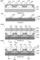
Figure 1A shows an epitaxial crystalline structure; -
Figure 1B shows the epitaxial crystalline structure ofFigure 1A that has been processed to form mesas; -
Figure 1C shows the structure ofFigure 1B that has been processed further; -
Figure 1D shows the structure ofFigure 1C that has been processed further; -
Figure 1E shows the structure ofFigure 1D that has been processed further; -
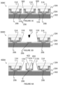
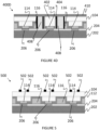
Figure 2 shows a processed backplane; -
Figure 3A shows the structure ofFigure 1E bonded to the backplane ofFigure 2 ; -
Figure 3B shows the structure ofFigure 3A that has been processed further; -
Figure 3C shows the structure ofFigure 3B that has been processed further; -
Figure 3D shows the structure ofFigure 3C that has been processed further to remove an LED die; -
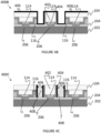
Figure 4A shows the structure ofFigure 3D with a replacement LED die; -
Figure 4B shows the structure ofFigure 4A that has been processed further; -
Figure 4C shows the structure ofFigure 4B that has been processed further; -
Figure 4D shows the structure ofFigure 4C that has been processed further; and -
Figure 5 shows the structure ofFigure 3B that has been processed further. - As described above, whilst monolithically grown LED devices beneficially enable the production of micro LED displays of ultra-fine pitch for high resolution display applications, there are difficulties associated with defective LED dies in the display arrays. The following process and structure described with reference to
Figures 1 to 5 enables a repair and replacement process for monolithic micro LED displays that achieves the necessary yield requirements whilst avoiding the need to transfer very high numbers of pixels by mass transfer pick and place based methods, for example. The method and structure enables display arrays of pixels to be provided, where the e.g., where the light emitting surface area of each pixel is less than or equal to 100µm2, and preferably less than or equal to 16µm2, and where the pixel pitch is less than 10µm and preferably less than 4µm and more preferably less than 3µm. - Advantageously, whilst the method and structure described here is used to replace defective dies, in further examples it is used to provide LED dies in the array that are configured to emit light of a different wavelength to the dies formed in the monolithically grown array of LED devices. For example, it is known to provide highly efficient LED devices based on nitride materials configured to emit light with a primary peak wavelength that is blue or green, but the provision of red light using such materials is more challenging. Gallium arsenide (GaAs) based materials, for example, are a more established technology for red-light emitting LED dies. Therefore, in an example, the method described herein is used to replace LED dies in monolithically grown arrays of nitride-based LED dies to provide light of different wavelengths. Advantageously, the number of dies that would be transferred into the monolithically grown array is much less than the total number of dies in the array, providing a more efficient and practical method for forming high resolution multi-colour micro LED arrays.
-
Figure 1A a cross sectional view of an epitaxialcrystalline structure 100A. The epitaxialcrystalline structure 100A is a structure formed from crystalline layers sequentially grown or deposited to provide a light emitting structure. The epitaxialcrystalline structure 100A is provided using metal organic chemical vapour deposition (MOCVD). In further examples, alternative and/or additional methods of growth and/or deposition are used to provide the epitaxialcrystalline structure 100A, for example molecular beam epitaxy (MBE). Advantageously, the epitaxialcrystalline structure 100A is provided in a continuous growth process and has a high crystalline quality and low defect density. In further examples, theepitaxial structure 100A is provided using multiple growth steps that enable the selective provision of particular qualities, for example different wavelengths of light emission upon radiative recombination of carriers from different areas of the epitaxialcrystalline structure 100A. - At
Figure 1A there is shown agrowth substrate 102, upon which there is grown an n-type region 104. Thegrowth substrate 102 is a silicon substrate. Alternatively, in further examples different material is used in order to provide agrowth substrate 102. The n-type region 104 is formed from n-type doped gallium nitride (GaN). In further examples, the n-type region 104 is formed from additional and/or alternative layers. For example, further buffer layers are included. On top of the n-type region 104 there is shown anactive region 106. Theactive region 106 is configured to emit light following the recombination of carriers injected from n-type and p-type regions. Theactive region 106 includes a multiple quantum well (MQW) structure. In further examples, the active region includes a single quantum well (SQW) structure. Theactive region 106 is configured to emit light with a primary peak wavelength that is controlled. In further examples, different portions of theactive region 106 are configured to emit light with different primary peak wavelengths. - On top of the
active region 106 there is shown a p-type region 108. The p-type region 108 is formed from p-type doped GaN. In further examples, the p-type region 108 is formed from additional and/or alternative layers. - The epitaxial
crystalline structure 100A is based on group III-V material (such as III-nitride material, e.g. GaN based materials). Whilst the structure is shown to be a nitride based structure, in further example different materials are used to provide a monolithic array of light emitting devices. Whilst the n-type region 104,active region 106 and p-type region 108 are shown, the skilled person understands in further examples further layers and/or alternative layers are used in order to provide the epitaxialcrystalline structure 100A. Once the epitaxialcrystalline structure 100A has been provided, as shown atFigure 1A , the epitaxial crystalline structure is processed in order to form multiple monolithically grown LED devices. This is shown atFigure 1B. Figure 1B shows a cross sectional view of a processedstructure 100B based on the epitaxialcrystalline structure 100A ofFigure 1A , wheremesas 110 have been formed. - The
mesas 110 each include portions of the p-type region 108 and theactive region 106. Themesas 110 are shown to have been formed on the n-type region 104. Themesas 110 are formed by selectively patterning and etching the epitaxialcrystalline structure 100A using known techniques. The skilled person understands that alternatively and/or additionally themesas 110 are formed from different and/or additional layers. - Once the
mesas 110 have been formed as shown atFigure 1B , the process moves toFigure 1C , where aconformal layer 112 is deposited on themesas 110.Figure 1C shows a cross sectional view of a processedstructure 100C that is a processed version of thestructure 100B ofFigure 1B . There is shown aconformal layer 112 formed on themesas 110. Theconformal layer 112 is deposited using known deposition techniques and is formed such that irreversible bonding with other layers is avoided at a later stage. Theconformal layer 112 is dielectric layer formed from silicon dioxide (SiO2). Alternatively and/or additionally in further examples, the conformal layer is a dielectric layer formed from a different material such as silicon nitride (Si3N4), photoresist such as Su-8, strontium fluoride (SrF2), polydimethylsiloxane (PDMS) or poly(methyl methacrylate) (PMMA). In further examples, the, or any other suitable material that enables reversible bonding at contacts without bonding by the portion of theconformal layer 112 that contacts a backplane to which the eventual structure is bonded. - The
conformal layer 112 is further processed in order to provide contacts to the p-type region 108. This is shown atFigure 1D. Figure 1D shows a cross sectional view of a processedepitaxial structure 100D that is a processed version of thestructure 100C described with respect toFigure 1C . Thestructure 100C ofFigure 1C is processed in order selectively to pattern and etch windows through theconformal layer 112, thereby to expose at least a portion of each of themesas 110 to which p-type contacts with the p-type region 108 are to be formed. Once the windows have been provided, p-type contacts are 114 are formed in the windows on themesas 110. - The electrical p-
type contacts 114 are formed from a metal. In an example, the metal is relatively highly reflective. Advantageously, the use of a relatively highly reflective electrical p-type contact 114 aids light extraction from the individual LED dies that are formed based on themesas 110 of the monolithically grown structural 100. The electrical p-type contacts 114 are formed in order to enable metal bonding (such as gold to gold (Au-Au) or copper to copper (Cu-Cu) bonding) and eutectic bonding (gold-tin (Au-Sn), copper-tin (Cu-Sn), indium-tin (InSn)) with a backplane. Alternatively and/or additionally, in further examples, the electrical p-type contacts 114 are formed from any suitability reflective and conductive material that can be used to form a reversible bond. In an example, the electrical p-type contacts 114 are formed from nickel and/or silver. The electrical p-type contacts 114 are used to form reversible bonds with a further backplane device and are therefore formed from a material that facilitates such reversible bonding. This is described in more detail below. - Once the electrical p-
type contacts 114 have been formed on themesas 110 as shown atFigure 1D , the process moves to that shown atFigure 1E . AtFigure 1E there is shown a cross sectional view of astructure 100E that is theepitaxial structure 100D ofFigure 1D that has been processed further in order to planiarise the structure. - Accordingly, in
Figure 1E there is shown material 116 deposited into the gaps formed between themesas 110, the surface of which has been planarised. Such planarization is achieved by deposition and chemical mechanical polishing of the material 116 to form a planar surface suitable for bonding to a further device. In further examples, alternative and/or additional methods are used in order to planarise the surface opposite thegrowth substrate 102. Thematerial 116 is a metal. Further examples, alternative and/oradditional material 116 is used, such as dielectric material. Once thestructure 100E has been provided, it is bonded to a backplane structure, as described below with reference toFigures 2 and3 . -
Figure 2 illustrates a processedbackplane 200 that has been processed in order to reversibly bond to a monolithically grown LED array, such as that described above with respect toFigure 1 . -
Figure 2 shows aCMOS backplane 202 upon which adielectric layer 204 has been deposited. Thedielectric layer 204 is processed in order to pattern and selectively etch windows in which material is deposited to formelectrical backplane contacts 206 using known techniques. The formation of windows exposes portions of theCMOS backplane 202 to which p-type contacts can be connected in order to control light emission from individual LED devices of in an array of LED devices. Whilst thebackplane 202 is aCMOS backplane 202, in further examples, additional and/or alternative backplanes are used to bond with an LED based structure to form a functioning display. - The
backplane contacts 206 are designed to form a reversible bond with the electrical p-type contacts 114 of thestructure 100E shown atFigure 1E . Accordingly, thebackplane contacts 206 are formed in order to enable metal bonding (such as gold to gold (Au-Au) or copper to copper (Cu-Cu) bonding) and eutectic bonding (such as gold-tin (Au-Sn), copper-tin (Cu-Sn), indium-tin (InSn)). Accordingly, the combination of material used to form the p-type contacts 114 of thestructure 100E shown atFigure 1E and theelectrical backplane contacts 206 is chosen to provide a combination of material that provides a reversible bond. - The
dielectric layer 204 is formed from silicon dioxide. Alternatively, and/or additionally thedielectric layer 204 is formed from silicon nitride, Su-8, SrF2, PDMS, PMMA or any other suitable material. Thedielectric layer 204 is formed such that it contacts with theconformal layer 112 and accordingly the aim is to prevent an oxide-oxide combination during bonding, such that thedielectric layer 204 does not form an irreversible bond with theconformal layer 112. Accordingly, the combination of material used to form theconformal layer 112 and thedielectric layer 204 is chosen to provide a combination of material that provides a reversible bond at the electrical contacts and not at other portions of the interface between the processedbackplane 200 and the monolithically grownepitaxial structure 100E. - Once the processed
backplane 200 and thestructure 100E have been provided, they are bonded together. This is shown atFigure 3A . - The
structure 300A ofFigure 3A shows a cross sectional view of thestructure 100E ofFigure 1E bonded to the processedstructure 200 ofFigure 2 . Thestructure 100E and the processedstructure 200 are bonded using thermocompression bonding techniques. In further examples, additional and/or alternative techniques are used to bond thestructures type contacts 114 are aligned with thebackplane contacts 206 of the processedbackplane 200. Whilst the combinedstructure 300A is shown in cross-section, the skilled person understands that the process is used for two dimensional arrays of LED devices that are monolithically grown ongrowth substrate 102 and bonded to a planar surface of a processedbackplane 200. The electrical p-type contacts 114 of the monolithically grown LED array are arranged in order to coincide withbackplane contacts 206 of thebackplane 200 thereby to form reversible bonds between the p-type contacts 114 of the monolithically grown LED array and thebackplane contacts 206 of thebackplane 200. - Once the
backplane 200 has been bonded to thestructure 100E in order to provide thestructure 300A ofFigure 3A , thegrowth substrate 102 of the epitaxialcrystalline structure 100A is removed. This is shown atFigure 3B. Figure 3B shows astructure 300B which is thestructure 300A ofFigure 3A that has been processed in order to remove thegrowth substrate 102. Once thegrowth substrate 102 has been removed, the n-type region 104 is exposed and can be selectively patterned and etched using known techniques. This is shown atFigure 3C . -
Figure 3C shows a cross sectional view of astructure 300C that is thestructure 300B ofFigure 3B that has been processed further in order selectively to etch through the n-type region 104, theconformal layer 112 and theplanarising material 116 in order to expose at least a portion of thedielectric layer 204 associated with thebackplane 200 through etchedchannels 302. Beneficially, such etching physically isolates LED dies (and therefore associated pixels) linked toindividual mesas 110 formed as described above with respect toFigure 1B . Such physical isolation of LED dies results in a discontinuous n-type region 104 as theetched channels 302 surround individual LED dies in order to physically isolate them. Advantageously, monolithically grown arrays of LED devices formed and enable high resolution arrays of pixels to be provided, whilst further enabling individual isolation of LED dies. - The physical isolation of individual LED dies that are each associated with a pixel means that individual pixels (or LED dies) are bonded to the
backplane 202 via a bond between thebackplane contacts 206 of the backplane and the electrical p-type contacts 114 of the LED dies. There is no significant bonding between thedielectric layer 204 andconformal layer 112, or theplanarising material 116 and thedielectric layer 204. The bonds between thebackplane contacts 206 of thebackplane 200 and the electrical p-type contacts 114 of the LED dies are reversible bonds, that is to say they can be broken in order to remove dies and reformed in order to bond replacement dies at the same site. Such reversible bonds are metal-metal bonds formed by thermocompression bonding, or eutectic bonds. In further examples, alternative and/or additional reversible bonds are formed using other suitable materials to provide reversible, conductive bonds between thebackplane 200 and the LED dies. - Once the individual dies have been isolated, they can then be tested in order to identify any defective dies. Once defective dies are identified, they can be removed by breaking the reversible bond between the
particular backplane contact 206 of the backplane and the associated p-type contact 114 of the associated defective die/pixel. Such dies, once identified can be removed. This is shown atFigure 3D . - At
Figure 3D there is shown a cross sectional view of thestructure 300C ofFigure 3C that has been processed further in order to provide thestructure 300D, whereby the central LED of theFigure 3C has been removed 304. Such removal is facilitated by heating the area associated with thebackplane contact 206 of thebackplane 200 and the electrical p-type contact 114 to above a temperature threshold to enable separate of the LED die from thebackplane 200. Such a temperature threshold to enable separation of the LED die from thebackplane 200 is the eutectic temperature of the eutectic bond. In further examples, the temperature threshold is based on a different measure, such a melting point of the metal, or other suitable temperate. Once the force bonding thebackplane contact 206 of thebackplane 200 and the electrical p-type contact 114 of the LED device is small enough, the defective die is removed through suction processes. In further examples, additional and/or alternative techniques are used to remove selected LED dies. Additionally, in further examples, plasma treatment is used to remove any residual material left on the surface from the removal process. Once defective dies have been removed, replacement dies can be deposited. This is shown atFigure 4A . -
Figure 4A shows a cross sectional view of astructure 400A that is thestructure 300D ofFigure 3D that has been processed further in order to provide a replacement LED die 402. The replacement LED die 402 (which includes an n-type region, p-type region, active region and p-type contact 414) is contacted with thebackplane 202 via thebackplane contact 206 of thebackplane 200 and the p-type contact 414 of thereplacement die LED 402 forming a eutectic bond between thebackplane contact 206 and the p-type contact 414. The LED die 402 has aconformal layer 404 formed on it in an analogous manner to that of theconformal layer 112 of the monolithically grown structure described with respect toFigures 1 to 3 . Whilst the bond is a eutectic bond, in further examples, alternative and/or additional bonding methods are used to secure the LED die 402 in thestructure 400A. - Whilst the process shown in respect to
Figure 3D and 4A illustrates the replacement of defective dies. Additionally and/or alternatively, in further examples LED dies may be removed in order to replace dies with different devices. For example, in order to insert red light emitting devices (such AlInGaP based red light emitting LED devices) into such monolithically grown arrays of light emitting devices with high quality blue and/or green light emitting LED device, where the method for forming high efficiency red light emitting LEDs differs from that used to form high efficiency blue and/or green light emitting LED devices. Advantageously, the number of replacement LED devices that are inserted to provide multi colour light emitting arrays is significantly lower than forming arrays of multi colour light emitting LED devices by pick and place technologies. - Once the replacement of a defective/unrequired die has been replaced as shown at
Figure 4A the process moves toFigure 4B . AtFigure 4B there is shown a cross sectional view of astructure 400A ofFigure 4A that has been processed to provide thestructure 400B ofFigure 4B . Thestructure 400B includes a metallicconformal layer 406 that has been deposited on thestructure 400A. Thisconformal layer 406 acts to reduce optical crosstalk between pixels associated with light emitting device dies in the display array. Once the metallicconformal layer 406 has been deposited atFigure 4B , the process moves toFigure 4C . - At
Figure 4C there is shown a cross sectional view of astructure 400C that is thestructure 400D ofFigure 4B that has been processed further in order to anisotopically etch the metallicconformal layer 406. Such anisotropic etching results in metal being left on the side walls of the light emitting dies. Once this anisotropic etch has been performed,filler material 408 is formed in the gaps between the LED devices.Such filler material 408 is deposited using known techniques and planarised using chemical mechanical polishing techniques. In further examples, alternative and/or additional methods are used in order to planarise the n-type side of the device of thestructure 400C. Once thestructure 400C has been planarised, the process moves to provide the structure shown atFigure 4D . -
Figure 4D shows a cross sectional view of astructure 400D that is the structure for 400C ofFigure 4C that has been processed in order in order to deposit a transparentconducting material layer 410. Such a layer is formed from indium tin oxide (ITO). Alternatively, and/or additionally, further examples different conducting transparent material is used. The transparentconducting material layer 410 enables formation of n-type contact with the n-type region 104 of multiple now isolated dies. Alternative and/or additional layers are used in further examples, for example metal tracks are used to assist with current spreading. - Accordingly, a method is described to provide repaired and/or replacement dies in a monolithically grown array of dies, where multiple dies provides a source of light at the light emitting surface associated with a pixel driven by the
CMOS backplane 202. - The skilled person understands that different and/or additional layers may be implemented throughout in order to provide advantageous functionality. For example
Figure 5 illustrates how lift-off of selected dies is enhanced.Figure 5 shows thestructure 500 that is the structure ofFigure 3B with additionalmagnetic material 502 formed in association with individual dies. Suchmagnetic material 502, (for example iron, nickel, cobalt) is deposited on part of the individual LED devices associated with pixels. In further examples, alternative and/or additional configurations are used in order to provide magnetic functionality associated with individual dies. Themagnetic material 502 is used in order to facilitate lift-off following isolation of pixels. Once repair and/or replacement of defective and/or unrequired dies has been performed, themagnetic material 502 is etched away, enabling the further deposition oftransparent conducting material 410 as described with respect toFigure 4D . - Advantageously, the methods described here enable repair in monolithic micro displays, allowing necessary yield requirements to be achieved. Further, the method enables different colour light emitting LED devices to be deposited on a monolithic display, such as red LED dies into blue/green monolithic displays.
- Whilst the processes described above are shown in a particular order, in further examples, alternative and/or additional steps are provided in order to enable the removal and replacement of LED dies in an array of LED devices that are monolithically grown.
- Whilst the epitaxial structures described herein are described with reference to n-type growth on a growth substrate prior to the formation of an active region and p-type region, with p-type contacts subsequently being formed on the top of mesas for connection with a backplane, the skilled person understands that the techniques, in further examples, are applicable to differently formed structures, for example based on a reversed growth sequence and/or with additional or alternative layers and/or with n-type contacts formed on mesas to form reversible bonds at corresponding contacts of a backplane.
- The invention is defined by the appended claims.
Claims (12)
- A method of forming a display comprising:planarising a backplane (200) comprising a plurality of backplane electrical contacts (206) to provide a first planarised surface;planarising a monolithic light emitting diode structure (100) comprising a plurality of electrical contacts (114) corresponding to the plurality of electrical contacts of the backplane to provide a second planarised surface;bonding the first planarised surface to the second planarised surface, wherein bonding comprises forming a reversible bond between at least one of the plurality of backplane electrical contacts and a corresponding electrical contact of the monolithic light emitting diode structure; andsubsequently selectively etching the monolithic light emitting diode structure to provide a plurality of physically isolated light emitting diode dies, thereby to enable removal and/or replacement of at least one physically isolated light emitting diode die by reversing the reversible bond between the at least one of the plurality of backplane electrical contacts and the corresponding electrical contact of the monolithic light emitting diode structure.
- The method according to claim 1, wherein the at least one of the backplane electrical contacts is reversibly bonded to the corresponding electrical contact of the monolithic light emitting diode structure using metal-to-metal bonding and/or eutectic bonding.
- The method according to any preceding claim, comprising:removing at least one physically isolated light emitting diode die; andreplacing the at least one physically isolated light emitting diode die with a different one or more light emitting diode dies.
- The method according to claim 3, wherein removing at least one physically isolated light emitting diode die comprises increasing the temperature of the display thereby to enable removal of the at least one physically isolated light emitting diode die at the reversible bond between the backplane electrical contact and the corresponding electrical contact associated with the monolithic light emitting diode structure, preferably wherein increasing the temperature of the display comprises increasing the temperature at the reversible bond to surpass a eutectic temperature of the reversible bond, preferably wherein the reversible bond comprises at least one of a AuSn eutectic bond, a CuSn eutectic bond and a InSn eutectic bond.
- The method according to claim 3, wherein removing at least one physically isolated light emitting diode die comprises overcoming an electrostatic force of the reversible bond, preferably wherein the electrostatic force of the reversible bond is the electrostatic force of at least one of a Au-Au metal bond and a Cu-Cu metal bond.
- The method of any preceding claim comprising:testing at least one of the plurality of physically isolated light emitting diode dies;identifying one or more defective light emitting diode dies;removing defective light emitting diode dies; andreplacing the one or more removed defective light emitting diode dies.
- The method according to any preceding claim, comprising:
forming a conformal metal layer (406) on at least a portion of the physically isolated light emitting diode dies, thereby to reduce optical cross talk between physically isolated light emitting diode dies. - The method according to any preceding claim, comprising:
forming a transparent electrically conductive layer (410) on the plurality of isolated light emitting diode dies, thereby to provide a common electrode. - The method according to any preceding claim, comprising:
forming one or more magnetic metal regions (502) associated with at least one of the physically isolated light emitting diode dies, thereby to facilitate removal of physically isolated light emitting diode dies. - The method according to any preceding claim, wherein at least one of the reversible bonds is at least partially laterally surrounded by a dielectric layer thereby to separate the backplane and the monolithic light emitting diode structure, preferably wherein the dielectric layer comprises at least one of SiO2, Si3N4, Su-8, SrF2, PDMS and PMMA.
- The method according to any preceding claim, wherein the plurality of contacts of the monolithic light emitting structure comprises a high reflectivity metal, preferably wherein the high reflectivity metal is one of Ni and Ag.
- The method according to any preceding claim, wherein removing material from the monolithic light emitting diode structure comprises forming a discontinuity in at least one layer of the monolithic light emitting diode structure, preferably wherein the at least one layer of the monolithic light emitting diode structure is an n-type layer, more preferably wherein the n-type layer is an n-doped gallium nitride layer.
Applications Claiming Priority (2)
| Application Number | Priority Date | Filing Date | Title |
|---|---|---|---|
| GB2009890.1A GB2596533B (en) | 2020-06-29 | 2020-06-29 | Hybrid microdisplay |
| PCT/GB2021/051573 WO2022003323A1 (en) | 2020-06-29 | 2021-06-22 | Method of forming a display and display |
Publications (2)
| Publication Number | Publication Date |
|---|---|
| EP4173046A1 EP4173046A1 (en) | 2023-05-03 |
| EP4173046B1 true EP4173046B1 (en) | 2025-01-15 |
Family
ID=71949625
Family Applications (1)
| Application Number | Title | Priority Date | Filing Date |
|---|---|---|---|
| EP21737742.3A Active EP4173046B1 (en) | 2020-06-29 | 2021-06-22 | Method of forming a display |
Country Status (8)
| Country | Link |
|---|---|
| US (1) | US12604583B2 (en) |
| EP (1) | EP4173046B1 (en) |
| JP (1) | JP7768912B2 (en) |
| KR (1) | KR102841839B1 (en) |
| CN (1) | CN115943496A (en) |
| GB (1) | GB2596533B (en) |
| TW (1) | TWI858270B (en) |
| WO (1) | WO2022003323A1 (en) |
Families Citing this family (5)
| Publication number | Priority date | Publication date | Assignee | Title |
|---|---|---|---|---|
| TWI808422B (en) | 2021-05-21 | 2023-07-11 | 錼創顯示科技股份有限公司 | Adhesive-layer structure and semiconductor structure |
| CN113299593B (en) * | 2021-05-21 | 2023-01-10 | 錼创显示科技股份有限公司 | Adhesion layer structure and semiconductor structure |
| WO2024193934A1 (en) * | 2023-03-23 | 2024-09-26 | Ams-Osram International Gmbh | Method for producing optoelectronic semiconductor chips and optoelectronic semiconductor chip |
| WO2025091226A1 (en) * | 2023-10-31 | 2025-05-08 | Jade Bird Display (shanghai) Limited | Micro-led array layer and micro-led display panel |
| WO2025239839A1 (en) * | 2024-05-17 | 2025-11-20 | New Silicon Corporation Pte Ltd | Pixel chip, display panel, method of fabricating a pixel chip |
Citations (1)
| Publication number | Priority date | Publication date | Assignee | Title |
|---|---|---|---|---|
| WO2019079381A1 (en) * | 2017-10-19 | 2019-04-25 | Spy Eye, Llc | Ultra-dense led projector |
Family Cites Families (20)
| Publication number | Priority date | Publication date | Assignee | Title |
|---|---|---|---|---|
| CN101005110A (en) * | 2007-01-12 | 2007-07-25 | 中国科学院上海微系统与信息技术研究所 | Method for realizing gallium nitride ELD vertical structure using metal bounding process |
| US8573469B2 (en) * | 2011-11-18 | 2013-11-05 | LuxVue Technology Corporation | Method of forming a micro LED structure and array of micro LED structures with an electrically insulating layer |
| KR20130092896A (en) | 2012-02-13 | 2013-08-21 | 엘지전자 주식회사 | Led display apparatus and manufacturing method thereof |
| FR3028672B1 (en) | 2014-11-18 | 2018-01-26 | Commissariat A L'energie Atomique Et Aux Energies Alternatives | OPTOELECTRONIC DEVICE WITH LIGHT EMITTING DIODES |
| CN105789122B (en) | 2014-12-12 | 2019-05-03 | 财团法人工业技术研究院 | Method for transferring photoelectric element |
| FR3033939B1 (en) | 2015-03-20 | 2018-04-27 | Commissariat A L'energie Atomique Et Aux Energies Alternatives | OPTOELECTRONIC DEVICE WITH ELECTROLUMINESCENT DIODE |
| WO2016188505A1 (en) * | 2015-05-22 | 2016-12-01 | Hiphoton Co., Ltd | Structure of a semiconductor array |
| EP3455882B1 (en) | 2016-05-13 | 2021-08-11 | Commissariat à l'Energie Atomique et aux Energies Alternatives | Method for producing an optoelectronic device comprising a plurality of gallium nitride diodes |
| US10361341B2 (en) | 2016-10-24 | 2019-07-23 | Glo Ab | Indium gallium nitride red light emitting diode and method of making thereof |
| US10902770B2 (en) * | 2016-12-22 | 2021-01-26 | Sharp Kabushiki Kaisha | Display device |
| JP6366799B1 (en) * | 2017-02-10 | 2018-08-01 | ルーメンス カンパニー リミテッド | Micro LED module and manufacturing method thereof |
| CN110462850B (en) | 2017-03-20 | 2024-04-16 | 上海显耀显示科技有限公司 | Semiconductor devices are made by stacking layers of micro-LEDs |
| JP6936867B2 (en) | 2017-11-10 | 2021-09-22 | シャープ株式会社 | Semiconductor modules, display devices, and methods for manufacturing semiconductor modules |
| JP7140315B2 (en) * | 2018-03-14 | 2022-09-21 | 京東方科技集團股▲ふん▼有限公司 | A method for transferring multiple micro-light emitting diodes onto a target substrate |
| FR3079350B1 (en) * | 2018-03-22 | 2020-03-27 | Commissariat A L'energie Atomique Et Aux Energies Alternatives | EMISSIBLE LED DISPLAY DEVICE AND METHOD FOR MANUFACTURING SUCH A DEVICE |
| KR20190114333A (en) * | 2018-03-29 | 2019-10-10 | (주)포인트엔지니어링 | Inspection method for micro led |
| CN110504346B (en) * | 2018-05-16 | 2021-06-25 | 鸿富锦精密工业(深圳)有限公司 | Micro LED display panel manufacturing method and display panel |
| US10985046B2 (en) * | 2018-06-22 | 2021-04-20 | Veeco Instruments Inc. | Micro-LED transfer methods using light-based debonding |
| JP7146595B2 (en) * | 2018-11-27 | 2022-10-04 | 株式会社ジャパンディスプレイ | DISPLAY PANEL, DISPLAY PANEL MANUFACTURING METHOD, AND SUBSTRATE |
| US10903267B2 (en) * | 2019-04-04 | 2021-01-26 | Bor-Jen Wu | System and method for making micro LED display |
-
2020
- 2020-06-29 GB GB2009890.1A patent/GB2596533B/en active Active
-
2021
- 2021-06-22 CN CN202180045289.7A patent/CN115943496A/en active Pending
- 2021-06-22 JP JP2022580838A patent/JP7768912B2/en active Active
- 2021-06-22 US US17/924,846 patent/US12604583B2/en active Active
- 2021-06-22 WO PCT/GB2021/051573 patent/WO2022003323A1/en not_active Ceased
- 2021-06-22 EP EP21737742.3A patent/EP4173046B1/en active Active
- 2021-06-22 KR KR1020227044541A patent/KR102841839B1/en active Active
- 2021-06-29 TW TW110123891A patent/TWI858270B/en active
Patent Citations (1)
| Publication number | Priority date | Publication date | Assignee | Title |
|---|---|---|---|---|
| WO2019079381A1 (en) * | 2017-10-19 | 2019-04-25 | Spy Eye, Llc | Ultra-dense led projector |
Also Published As
| Publication number | Publication date |
|---|---|
| JP2023532906A (en) | 2023-08-01 |
| WO2022003323A1 (en) | 2022-01-06 |
| TWI858270B (en) | 2024-10-11 |
| GB2596533B (en) | 2023-02-15 |
| JP7768912B2 (en) | 2025-11-12 |
| US12604583B2 (en) | 2026-04-14 |
| CN115943496A (en) | 2023-04-07 |
| TW202205712A (en) | 2022-02-01 |
| EP4173046A1 (en) | 2023-05-03 |
| US20230187592A1 (en) | 2023-06-15 |
| KR102841839B1 (en) | 2025-08-04 |
| GB202009890D0 (en) | 2020-08-12 |
| KR20230029648A (en) | 2023-03-03 |
| GB2596533A (en) | 2022-01-05 |
Similar Documents
| Publication | Publication Date | Title |
|---|---|---|
| US12604583B2 (en) | Hybrid microdisplay | |
| US11715730B2 (en) | Direct-bonded LED arrays including optical elements configured to transmit optical signals from LED elements | |
| CN114188459B (en) | Micro light-emitting diode display device and manufacturing method thereof | |
| KR102814860B1 (en) | luminescent array | |
| CN115176347B (en) | High-resolution monolithic RGB array | |
| CN114759130B (en) | Micro-LED display chip and preparation method thereof | |
| US12040344B2 (en) | Light emitting device and display apparatus having the same | |
| KR20250099328A (en) | Multicolor luminescent micro LED display and its manufacturing method | |
| KR102832422B1 (en) | Monolithic electronic devices | |
| US20240313182A1 (en) | Light emitting device and display apparatus having the same | |
| WO2024119056A1 (en) | Display including lateral-structure multicolor light emitting device pixels and method of fabrication thereof | |
| US12615899B2 (en) | Light emitting device and display apparatus having the same | |
| KR102721221B1 (en) | Semiconductor stacked structure using semiconductor device template and method for manufacturing same | |
| CN115458663B (en) | A full-color flip-chip light-emitting diode chip unit, preparation method and display screen | |
| US20230223494A1 (en) | Light emitting diodes and method of making thereof by selectively growing active layers from trench separated areas | |
| EP4250378B1 (en) | Method for forming resonant cavity light emitting elements and optical device comprising said elements | |
| KR20260007646A (en) | Display device and method for manufacturing a display device |
Legal Events
| Date | Code | Title | Description |
|---|---|---|---|
| STAA | Information on the status of an ep patent application or granted ep patent |
Free format text: STATUS: UNKNOWN |
|
| STAA | Information on the status of an ep patent application or granted ep patent |
Free format text: STATUS: THE INTERNATIONAL PUBLICATION HAS BEEN MADE |
|
| PUAI | Public reference made under article 153(3) epc to a published international application that has entered the european phase |
Free format text: ORIGINAL CODE: 0009012 |
|
| STAA | Information on the status of an ep patent application or granted ep patent |
Free format text: STATUS: REQUEST FOR EXAMINATION WAS MADE |
|
| 17P | Request for examination filed |
Effective date: 20221025 |
|
| AK | Designated contracting states |
Kind code of ref document: A1 Designated state(s): AL AT BE BG CH CY CZ DE DK EE ES FI FR GB GR HR HU IE IS IT LI LT LU LV MC MK MT NL NO PL PT RO RS SE SI SK SM TR |
|
| DAV | Request for validation of the european patent (deleted) | ||
| DAX | Request for extension of the european patent (deleted) | ||
| GRAP | Despatch of communication of intention to grant a patent |
Free format text: ORIGINAL CODE: EPIDOSNIGR1 |
|
| STAA | Information on the status of an ep patent application or granted ep patent |
Free format text: STATUS: GRANT OF PATENT IS INTENDED |
|
| INTG | Intention to grant announced |
Effective date: 20240916 |
|
| P01 | Opt-out of the competence of the unified patent court (upc) registered |
Free format text: CASE NUMBER: APP_58126/2024 Effective date: 20241024 |
|
| GRAS | Grant fee paid |
Free format text: ORIGINAL CODE: EPIDOSNIGR3 |
|
| GRAA | (expected) grant |
Free format text: ORIGINAL CODE: 0009210 |
|
| STAA | Information on the status of an ep patent application or granted ep patent |
Free format text: STATUS: THE PATENT HAS BEEN GRANTED |
|
| RBV | Designated contracting states (corrected) |
Designated state(s): AL AT BE BG CH CY CZ DE DK EE ES FI FR GR HR HU IE IS IT LI LT LU LV MC MK MT NL NO PL PT RO RS SE SI SK SM TR |
|
| AK | Designated contracting states |
Kind code of ref document: B1 Designated state(s): AL AT BE BG CH CY CZ DE DK EE ES FI FR GR HR HU IE IS IT LI LT LU LV MC MK MT NL NO PL PT RO RS SE SI SK SM TR |
|
| REG | Reference to a national code |
Ref country code: CH Ref legal event code: EP |
|
| REG | Reference to a national code |
Ref country code: DE Ref legal event code: R096 Ref document number: 602021024994 Country of ref document: DE |
|
| REG | Reference to a national code |
Ref country code: IE Ref legal event code: FG4D |
|
| REG | Reference to a national code |
Ref country code: NL Ref legal event code: MP Effective date: 20250115 |
|
| PG25 | Lapsed in a contracting state [announced via postgrant information from national office to epo] |
Ref country code: NL Free format text: LAPSE BECAUSE OF FAILURE TO SUBMIT A TRANSLATION OF THE DESCRIPTION OR TO PAY THE FEE WITHIN THE PRESCRIBED TIME-LIMIT Effective date: 20250115 |
|
| PG25 | Lapsed in a contracting state [announced via postgrant information from national office to epo] |
Ref country code: RS Free format text: LAPSE BECAUSE OF FAILURE TO SUBMIT A TRANSLATION OF THE DESCRIPTION OR TO PAY THE FEE WITHIN THE PRESCRIBED TIME-LIMIT Effective date: 20250415 |
|
| PG25 | Lapsed in a contracting state [announced via postgrant information from national office to epo] |
Ref country code: FI Free format text: LAPSE BECAUSE OF FAILURE TO SUBMIT A TRANSLATION OF THE DESCRIPTION OR TO PAY THE FEE WITHIN THE PRESCRIBED TIME-LIMIT Effective date: 20250115 |
|
| PG25 | Lapsed in a contracting state [announced via postgrant information from national office to epo] |
Ref country code: PL Free format text: LAPSE BECAUSE OF FAILURE TO SUBMIT A TRANSLATION OF THE DESCRIPTION OR TO PAY THE FEE WITHIN THE PRESCRIBED TIME-LIMIT Effective date: 20250115 |
|
| PGFP | Annual fee paid to national office [announced via postgrant information from national office to epo] |
Ref country code: DE Payment date: 20250618 Year of fee payment: 5 |
|
| PG25 | Lapsed in a contracting state [announced via postgrant information from national office to epo] |
Ref country code: ES Free format text: LAPSE BECAUSE OF FAILURE TO SUBMIT A TRANSLATION OF THE DESCRIPTION OR TO PAY THE FEE WITHIN THE PRESCRIBED TIME-LIMIT Effective date: 20250115 |
|
| REG | Reference to a national code |
Ref country code: LT Ref legal event code: MG9D |
|
| PG25 | Lapsed in a contracting state [announced via postgrant information from national office to epo] |
Ref country code: NO Free format text: LAPSE BECAUSE OF FAILURE TO SUBMIT A TRANSLATION OF THE DESCRIPTION OR TO PAY THE FEE WITHIN THE PRESCRIBED TIME-LIMIT Effective date: 20250415 Ref country code: IS Free format text: LAPSE BECAUSE OF FAILURE TO SUBMIT A TRANSLATION OF THE DESCRIPTION OR TO PAY THE FEE WITHIN THE PRESCRIBED TIME-LIMIT Effective date: 20250515 |
|
| REG | Reference to a national code |
Ref country code: AT Ref legal event code: MK05 Ref document number: 1760418 Country of ref document: AT Kind code of ref document: T Effective date: 20250115 |
|
| PG25 | Lapsed in a contracting state [announced via postgrant information from national office to epo] |
Ref country code: HR Free format text: LAPSE BECAUSE OF FAILURE TO SUBMIT A TRANSLATION OF THE DESCRIPTION OR TO PAY THE FEE WITHIN THE PRESCRIBED TIME-LIMIT Effective date: 20250115 |
|
| PG25 | Lapsed in a contracting state [announced via postgrant information from national office to epo] |
Ref country code: PT Free format text: LAPSE BECAUSE OF FAILURE TO SUBMIT A TRANSLATION OF THE DESCRIPTION OR TO PAY THE FEE WITHIN THE PRESCRIBED TIME-LIMIT Effective date: 20250515 Ref country code: LV Free format text: LAPSE BECAUSE OF FAILURE TO SUBMIT A TRANSLATION OF THE DESCRIPTION OR TO PAY THE FEE WITHIN THE PRESCRIBED TIME-LIMIT Effective date: 20250115 |
|
| PGFP | Annual fee paid to national office [announced via postgrant information from national office to epo] |
Ref country code: FR Payment date: 20250627 Year of fee payment: 5 |
|
| PG25 | Lapsed in a contracting state [announced via postgrant information from national office to epo] |
Ref country code: BG Free format text: LAPSE BECAUSE OF FAILURE TO SUBMIT A TRANSLATION OF THE DESCRIPTION OR TO PAY THE FEE WITHIN THE PRESCRIBED TIME-LIMIT Effective date: 20250115 Ref country code: GR Free format text: LAPSE BECAUSE OF FAILURE TO SUBMIT A TRANSLATION OF THE DESCRIPTION OR TO PAY THE FEE WITHIN THE PRESCRIBED TIME-LIMIT Effective date: 20250416 |
|
| PG25 | Lapsed in a contracting state [announced via postgrant information from national office to epo] |
Ref country code: AT Free format text: LAPSE BECAUSE OF FAILURE TO SUBMIT A TRANSLATION OF THE DESCRIPTION OR TO PAY THE FEE WITHIN THE PRESCRIBED TIME-LIMIT Effective date: 20250115 |
|
| PGFP | Annual fee paid to national office [announced via postgrant information from national office to epo] |
Ref country code: IE Payment date: 20250618 Year of fee payment: 5 |
|
| PG25 | Lapsed in a contracting state [announced via postgrant information from national office to epo] |
Ref country code: SE Free format text: LAPSE BECAUSE OF FAILURE TO SUBMIT A TRANSLATION OF THE DESCRIPTION OR TO PAY THE FEE WITHIN THE PRESCRIBED TIME-LIMIT Effective date: 20250115 |
|
| PG25 | Lapsed in a contracting state [announced via postgrant information from national office to epo] |
Ref country code: SM Free format text: LAPSE BECAUSE OF FAILURE TO SUBMIT A TRANSLATION OF THE DESCRIPTION OR TO PAY THE FEE WITHIN THE PRESCRIBED TIME-LIMIT Effective date: 20250115 |
|
| PG25 | Lapsed in a contracting state [announced via postgrant information from national office to epo] |
Ref country code: DK Free format text: LAPSE BECAUSE OF FAILURE TO SUBMIT A TRANSLATION OF THE DESCRIPTION OR TO PAY THE FEE WITHIN THE PRESCRIBED TIME-LIMIT Effective date: 20250115 |
|
| PGFP | Annual fee paid to national office [announced via postgrant information from national office to epo] |
Ref country code: IT Payment date: 20250619 Year of fee payment: 5 |
|
| REG | Reference to a national code |
Ref country code: DE Ref legal event code: R097 Ref document number: 602021024994 Country of ref document: DE |
|
| PG25 | Lapsed in a contracting state [announced via postgrant information from national office to epo] |
Ref country code: EE Free format text: LAPSE BECAUSE OF FAILURE TO SUBMIT A TRANSLATION OF THE DESCRIPTION OR TO PAY THE FEE WITHIN THE PRESCRIBED TIME-LIMIT Effective date: 20250115 Ref country code: CZ Free format text: LAPSE BECAUSE OF FAILURE TO SUBMIT A TRANSLATION OF THE DESCRIPTION OR TO PAY THE FEE WITHIN THE PRESCRIBED TIME-LIMIT Effective date: 20250115 |
|
| PG25 | Lapsed in a contracting state [announced via postgrant information from national office to epo] |
Ref country code: RO Free format text: LAPSE BECAUSE OF FAILURE TO SUBMIT A TRANSLATION OF THE DESCRIPTION OR TO PAY THE FEE WITHIN THE PRESCRIBED TIME-LIMIT Effective date: 20250115 |
|
| PG25 | Lapsed in a contracting state [announced via postgrant information from national office to epo] |
Ref country code: SK Free format text: LAPSE BECAUSE OF FAILURE TO SUBMIT A TRANSLATION OF THE DESCRIPTION OR TO PAY THE FEE WITHIN THE PRESCRIBED TIME-LIMIT Effective date: 20250115 |
|
| PLBE | No opposition filed within time limit |
Free format text: ORIGINAL CODE: 0009261 |
|
| STAA | Information on the status of an ep patent application or granted ep patent |
Free format text: STATUS: NO OPPOSITION FILED WITHIN TIME LIMIT |
|
| REG | Reference to a national code |
Ref country code: CH Ref legal event code: L10 Free format text: ST27 STATUS EVENT CODE: U-0-0-L10-L00 (AS PROVIDED BY THE NATIONAL OFFICE) Effective date: 20251126 |
|
| 26N | No opposition filed |
Effective date: 20251016 |
|
| REG | Reference to a national code |
Ref country code: CH Ref legal event code: H13 Free format text: ST27 STATUS EVENT CODE: U-0-0-H10-H13 (AS PROVIDED BY THE NATIONAL OFFICE) Effective date: 20260127 |
|
| PG25 | Lapsed in a contracting state [announced via postgrant information from national office to epo] |
Ref country code: MC Free format text: LAPSE BECAUSE OF FAILURE TO SUBMIT A TRANSLATION OF THE DESCRIPTION OR TO PAY THE FEE WITHIN THE PRESCRIBED TIME-LIMIT Effective date: 20250115 |
|
| PG25 | Lapsed in a contracting state [announced via postgrant information from national office to epo] |
Ref country code: LU Free format text: LAPSE BECAUSE OF NON-PAYMENT OF DUE FEES Effective date: 20250622 |
|
| REG | Reference to a national code |
Ref country code: BE Ref legal event code: MM Effective date: 20250630 |
|
| PG25 | Lapsed in a contracting state [announced via postgrant information from national office to epo] |
Ref country code: BE Free format text: LAPSE BECAUSE OF NON-PAYMENT OF DUE FEES Effective date: 20250630 |
|
| PG25 | Lapsed in a contracting state [announced via postgrant information from national office to epo] |
Ref country code: CH Free format text: LAPSE BECAUSE OF NON-PAYMENT OF DUE FEES Effective date: 20250630 |