EP4170915A1 - Electronic device - Google Patents
Electronic device Download PDFInfo
- Publication number
- EP4170915A1 EP4170915A1 EP22198253.1A EP22198253A EP4170915A1 EP 4170915 A1 EP4170915 A1 EP 4170915A1 EP 22198253 A EP22198253 A EP 22198253A EP 4170915 A1 EP4170915 A1 EP 4170915A1
- Authority
- EP
- European Patent Office
- Prior art keywords
- signal line
- electronic element
- conductive layer
- electronic device
- voltage
- Prior art date
- Legal status (The legal status is an assumption and is not a legal conclusion. Google has not performed a legal analysis and makes no representation as to the accuracy of the status listed.)
- Pending
Links
- 239000000758 substrate Substances 0.000 claims abstract description 25
- 238000009413 insulation Methods 0.000 claims description 33
- 101100489584 Solanum lycopersicum TFT1 gene Proteins 0.000 claims description 6
- 101100214488 Solanum lycopersicum TFT2 gene Proteins 0.000 claims description 6
- 101100214491 Solanum lycopersicum TFT3 gene Proteins 0.000 claims description 6
- 239000003990 capacitor Substances 0.000 claims description 6
- 230000010287 polarization Effects 0.000 claims description 6
- 230000000149 penetrating effect Effects 0.000 claims 1
- 239000010410 layer Substances 0.000 description 115
- 239000010408 film Substances 0.000 description 13
- 239000000463 material Substances 0.000 description 13
- 229910000679 solder Inorganic materials 0.000 description 13
- 239000000470 constituent Substances 0.000 description 6
- 230000001105 regulatory effect Effects 0.000 description 6
- 239000007787 solid Substances 0.000 description 5
- 239000004973 liquid crystal related substance Substances 0.000 description 4
- XUIMIQQOPSSXEZ-UHFFFAOYSA-N Silicon Chemical compound [Si] XUIMIQQOPSSXEZ-UHFFFAOYSA-N 0.000 description 3
- PCHJSUWPFVWCPO-UHFFFAOYSA-N gold Chemical compound [Au] PCHJSUWPFVWCPO-UHFFFAOYSA-N 0.000 description 3
- 229910052737 gold Inorganic materials 0.000 description 3
- 239000010931 gold Substances 0.000 description 3
- 229910052710 silicon Inorganic materials 0.000 description 3
- 239000010703 silicon Substances 0.000 description 3
- VYPSYNLAJGMNEJ-UHFFFAOYSA-N silicon dioxide Inorganic materials O=[Si]=O VYPSYNLAJGMNEJ-UHFFFAOYSA-N 0.000 description 3
- 239000010409 thin film Substances 0.000 description 3
- RYGMFSIKBFXOCR-UHFFFAOYSA-N Copper Chemical compound [Cu] RYGMFSIKBFXOCR-UHFFFAOYSA-N 0.000 description 2
- PXHVJJICTQNCMI-UHFFFAOYSA-N Nickel Chemical compound [Ni] PXHVJJICTQNCMI-UHFFFAOYSA-N 0.000 description 2
- 239000004642 Polyimide Substances 0.000 description 2
- 229910052581 Si3N4 Inorganic materials 0.000 description 2
- BQCADISMDOOEFD-UHFFFAOYSA-N Silver Chemical compound [Ag] BQCADISMDOOEFD-UHFFFAOYSA-N 0.000 description 2
- 229910052782 aluminium Inorganic materials 0.000 description 2
- XAGFODPZIPBFFR-UHFFFAOYSA-N aluminium Chemical compound [Al] XAGFODPZIPBFFR-UHFFFAOYSA-N 0.000 description 2
- 239000004020 conductor Substances 0.000 description 2
- 229910052802 copper Inorganic materials 0.000 description 2
- 239000010949 copper Substances 0.000 description 2
- AMGQUBHHOARCQH-UHFFFAOYSA-N indium;oxotin Chemical compound [In].[Sn]=O AMGQUBHHOARCQH-UHFFFAOYSA-N 0.000 description 2
- 229910001092 metal group alloy Inorganic materials 0.000 description 2
- 229920000139 polyethylene terephthalate Polymers 0.000 description 2
- 239000005020 polyethylene terephthalate Substances 0.000 description 2
- 229920001721 polyimide Polymers 0.000 description 2
- 229920000642 polymer Polymers 0.000 description 2
- 239000002096 quantum dot Substances 0.000 description 2
- HQVNEWCFYHHQES-UHFFFAOYSA-N silicon nitride Chemical compound N12[Si]34N5[Si]62N3[Si]51N64 HQVNEWCFYHHQES-UHFFFAOYSA-N 0.000 description 2
- 229910052814 silicon oxide Inorganic materials 0.000 description 2
- 229910052709 silver Inorganic materials 0.000 description 2
- 239000004332 silver Substances 0.000 description 2
- 239000002356 single layer Substances 0.000 description 2
- OAICVXFJPJFONN-UHFFFAOYSA-N Phosphorus Chemical compound [P] OAICVXFJPJFONN-UHFFFAOYSA-N 0.000 description 1
- XHCLAFWTIXFWPH-UHFFFAOYSA-N [O-2].[O-2].[O-2].[O-2].[O-2].[V+5].[V+5] Chemical compound [O-2].[O-2].[O-2].[O-2].[O-2].[V+5].[V+5] XHCLAFWTIXFWPH-UHFFFAOYSA-N 0.000 description 1
- 230000005540 biological transmission Effects 0.000 description 1
- 239000000919 ceramic Substances 0.000 description 1
- 230000008878 coupling Effects 0.000 description 1
- 238000010168 coupling process Methods 0.000 description 1
- 238000005859 coupling reaction Methods 0.000 description 1
- 239000011521 glass Substances 0.000 description 1
- 238000007654 immersion Methods 0.000 description 1
- 230000006698 induction Effects 0.000 description 1
- 230000002452 interceptive effect Effects 0.000 description 1
- 229910052759 nickel Inorganic materials 0.000 description 1
- 230000002093 peripheral effect Effects 0.000 description 1
- 229920000515 polycarbonate Polymers 0.000 description 1
- 239000004417 polycarbonate Substances 0.000 description 1
- -1 polyethylene terephthalate Polymers 0.000 description 1
- 239000010453 quartz Substances 0.000 description 1
- 229910052594 sapphire Inorganic materials 0.000 description 1
- 239000010980 sapphire Substances 0.000 description 1
- 239000004065 semiconductor Substances 0.000 description 1
- 229910001935 vanadium oxide Inorganic materials 0.000 description 1
Images


Classifications
-
- H—ELECTRICITY
- H04—ELECTRIC COMMUNICATION TECHNIQUE
- H04B—TRANSMISSION
- H04B1/00—Details of transmission systems, not covered by a single one of groups H04B3/00 - H04B13/00; Details of transmission systems not characterised by the medium used for transmission
- H04B1/02—Transmitters
- H04B1/04—Circuits
-
- H—ELECTRICITY
- H03—ELECTRONIC CIRCUITRY
- H03H—IMPEDANCE NETWORKS, e.g. RESONANT CIRCUITS; RESONATORS
- H03H7/00—Multiple-port networks comprising only passive electrical elements as network components
-
- H—ELECTRICITY
- H01—ELECTRIC ELEMENTS
- H01P—WAVEGUIDES; RESONATORS, LINES, OR OTHER DEVICES OF THE WAVEGUIDE TYPE
- H01P3/00—Waveguides; Transmission lines of the waveguide type
- H01P3/12—Hollow waveguides
-
- H—ELECTRICITY
- H03—ELECTRONIC CIRCUITRY
- H03C—MODULATION
- H03C3/00—Angle modulation
Definitions
- the disclosure relates to an electronic device, and in particular to an electronic device having a modulation unit capable of modulating a phase, a bandwidth, an intensity, or a polarization state of an electromagnetic wave.
- Electronic devices or splicing electronic devices have been widely used in mobile phones, televisions, monitors, tablet computers, car displays, wearable devices, and desktop computers. With the vigorous development of electronic devices, the quality requirements for electronic devices are increasing, and such electronic products can often be used as electronic modulation devices at the same time, for example, as antenna devices that can modulate electromagnetic waves. However, the existing antenna devices still do not meet the requirements of consumers in all aspects.
- the disclosure provides an electronic device having a modulation unit capable of modulating a phase, a bandwidth, an intensity, or a polarization state of an electromagnetic wave.
- the electronic device includes a substrate and multiple modulation units.
- the modulation units are disposed on the substrate.
- Each modulation unit includes a first electronic element, a second electronic element, a first signal line, a second signal line, and a third signal line.
- the first signal line provides a first voltage to the first electronic element.
- the second signal line provides a second voltage to the second electronic element.
- the third signal line provides a third voltage to the first electronic element and/or the second electronic element.
- the first voltage is different from the second voltage
- the third voltage is different from the first voltage and/or the second voltage.
- first, second, third may be used to describe various constituent elements
- the constituent elements are not limited by the terms. The terms are only used to distinguish a single constituent element from other constituent elements in the specification. The same terms may not be used in the claims, but replaced by first, second, third... according to the order in which the elements are declared in the claims. Therefore, a first constituent element in the following specification may be a second constituent element in the claims.
- the terms “about”, “approximately”, “substantially”, and “roughly” generally mean within 0.5%, 1%, 2%, 3%, 5%, or 10% of a given value or range.
- the number given here is an approximate number, that is, the meaning of "about”, “approximately”, “substantially”, or “roughly” may still be implied without the specific description of "about”, “approximately”, “substantially”, and “roughly”.
- connection and “interconnection” may mean that two structures are in direct contact or may also mean that two structures are not in direct contact, wherein there is another structure disposed between the two structures, unless otherwise defined.
- the terms related to bonding and connection may also include the case where the two structures are both movable or the two structures are both fixed.
- the term “coupling” includes any direct and indirect means of electrical connection.
- the electronic device may include a display device, an antenna device (for example, a liquid crystal antenna), a sensing device, a light emitting device, a touch device, or a splicing device, but not limited thereto.
- the electronic device may include a bendable or flexible electronic device.
- the appearance of the electronic device may be rectangular, circular, polygonal, a shape with curved edges, or other suitable shapes.
- the display device may, for example, include a light emitting diode (LED), liquid crystal, fluorescence, phosphor, quantum dot (QD), other suitable materials, or a combination of the foregoing, but not limited thereto.
- LED light emitting diode
- QD quantum dot
- the light emitting diode may include, for example, an organic light emitting diode (OLED), an inorganic light emitting diode, a mini LED, a micro LED, a QDLED, other suitable materials, or any combination of the foregoing, but not limited thereto.
- the display device may also include, for example, a splicing display device, but not limited thereto.
- the antenna device may be, for example, a liquid crystal antenna, but not limited thereto.
- the antenna device may include, for example, an antenna splicing device, but not limited thereto. It should be noted that the electronic device may be any combination of the foregoing, but not limited thereto.
- the appearance of the electronic device may be rectangular, circular, polygonal, a shape with curved edges, or other suitable shapes.
- the electronic device may have a peripheral system such as a driving system, a control system, a light source system, and a shelf system to support the display device, the antenna device, or the splicing device.
- a peripheral system such as a driving system, a control system, a light source system, and a shelf system to support the display device, the antenna device, or the splicing device.
- FIG. 1A is a schematic partial top view of an electronic device according to an embodiment of the disclosure.
- FIG. 1B is a schematic cross-sectional view of the electronic device of FIG. 1A along a section line I-I'.
- FIG. 1A omits to show several elements in an electronic device 10.
- the electronic device 10 of this embodiment includes a substrate 101 and multiple modulation units 100.
- the modulation units 100 are disposed on the substrate 101 and are used to modulate an intensity, a bandwidth, or a phase of a received electromagnetic wave signal (or light signal, but not limited thereto).
- each modulation unit 100 includes a first conductive layer pattern 120, a first insulation layer 130, a first electronic element 141, a second electronic element 142, a first signal line 151, a second signal line 152, and a third signal line 153.
- the substrate 101 may include a hard substrate, a soft substrate, or a combination of the foregoing.
- the material of the substrate 101 may include glass, quartz, silicon wafer, sapphire, III-V semiconductor material, ceramics, polycarbonate (PC), polyimide (PI), polyethylene terephthalate (PET), other suitable substrate materials, or a combination of the foregoing, but not limited thereto.
- the substrate 101 may be a printed circuit board.
- a conductive layer including the first conductive layer pattern 120 is disposed on the substrate 101.
- the first conductive layer pattern 120 includes a first part 121, a second part 122, and a third part 123.
- the first part 121, the second part 122, and the third part 123 are separated from each other.
- the third part 123 is located between the first part 121 and the second part 122.
- the first conductive layer pattern 120 may resonate with the received electromagnetic wave signal (or light signal).
- the material of the first conductive layer pattern 120 may include copper, aluminum, silver, gold, indium tin oxide (ITO), metal alloy, other suitable conductive materials, or a combination of the foregoing materials, but not limited thereto.
- the pattern of the first conductive layer pattern 120 may include the pattern of the first part 121, the pattern of the second part 122, and the pattern of the third part 123.
- the pattern of the first part 121 and the pattern of the second part 122 may be regarded as E-shaped, and the pattern of the third part 123 may be regarded as a solid square shape, but not limited thereto.
- the pattern of the first part 121, the pattern of the second part 122, and the pattern of the third part 123 are separated from each other.
- the pattern of the first part 121 and the pattern of the second part 122 may surround the pattern of the third part 123, and the pattern of the first part 121 and the pattern of the second part 122 may be disposed on two sides of the pattern of the third part 123 in a mirroring manner, but not limited thereto.
- the first part of the insulation layer that is, the first insulation layer 130 is disposed on the first conductive layer pattern 120 to cover a part of the first conductive layer pattern 120 and cover a part of the substrate 101 exposed by an opening between the first conductive layer patterns 120.
- the first insulation layer 1 30 may expose another part of the first conductive layer pattern 120 for disposing a bonding pad 161, a bonding pad 162, a bonding pad 163, and a bonding pad 164.
- the first insulation layer 130 may be a single-layer or multi-layer structure, and the material of the first insulation layer 130 may include a polymer thin film, silicon nitride, silicon oxide, silicon oxynitride, or a combination of the foregoing, but not limited thereto.
- each modulation unit 100 further includes a bonding pad 161, a bonding pad 162, a bonding pad 163, and a bonding pad 164, wherein the bonding pad 161 and the bonding pad 163 are respectively disposed between the first conductive layer pattern 120 and the first electronic element 141, and the bonding pad 162 and the bonding pad 164 are respectively disposed between the first conductive layer pattern 120 and the second electronic element 142.
- the bonding pad 161 is disposed on the first part 121 of the first conductive layer pattern 120 to contact the first part 121.
- the bonding pad 162 is disposed on the second part 122 of the first conductive layer pattern 120 to contact the second part 122.
- the bonding pad 163 and the bonding pad 164 are respectively disposed on the third part 123 of the first conductive layer pattern 120 to contact the third part 123.
- the materials of the bonding pad 161, the bonding pad 162, the bonding pad 163, and the bonding pad 164 may include copper, aluminum, silver, gold, indium tin oxide, metal alloys (for example, electroless nickel immersion gold (ENIG)), other suitable conductive materials, or a combination of the foregoing materials, but not limited thereto.
- each modulation unit 100 further includes multiple solder balls 165, 166, 167, and 168, which are respectively disposed on the bonding pad 161, the bonding pad 162, the bonding pad 163, and the bonding pad 164.
- the solder ball 165 may contact the bonding pad 161, the solder ball 166 may contact the bonding pad 162, the solder ball 167 may contact the bonding pad 163, and the solder ball 168 may contact the bonding pad 164.
- the first electronic element 141 and the second electronic element 142 are disposed on the first signal line 151, the second signal line 152, and the third signal line 153.
- the first electronic element 141 has a pad 141a and a pad 141b
- the second electronic element 142 has a pad 142a and a pad 142b.
- the first electronic element 141 may be bonded to the bonding pad 161 through the pad 141a and the solder ball 165, and may be bonded to the bonding pad 163 through the pad 141b and the solder ball 167.
- the second electronic element 142 may be bonded to the bonding pad 162 through the pad 142a and the solder ball 166, and may be bonded to the bonding pad 164 through the pad 142b and the solder ball 168.
- the first electronic element 141 may be bonded to the first conductive layer pattern 120 through the bonding pad 161 and the bonding pad 163
- the second electronic element 142 may be bonded to the first conductive layer pattern 120 through the bonding pad 162 and the bonding pad 164.
- the first electronic element 141 and the second electronic element 142 may have the characteristic of being sensitive to external stimuli, and the first electronic element 141 and the second electronic element 142 may be regulated by the external stimuli to change their own characteristics, wherein the external stimulus is, for example, voltage, current, temperature, etc., and their own characteristic is, for example, a capacitance value or a resistance value, but not limited thereto.
- the first electronic element 141 and the second electronic element 142 may include, for example, capacitors, inductors, or resistors, but not limited thereto.
- the modulation unit 100 may regulate the capacitors by applying voltages to change the capacitance values of the capacitors.
- the first electronic element 141 and the second electronic element 142 may also be, for example, electronic elements containing materials sensitive to external stimuli, electronic elements containing elements sensitive to external stimuli, or electronic elements containing structures sensitive to external stimuli.
- the material sensitive to external stimuli may be, for example, liquid crystal, vanadium oxide, etc.
- the element sensitive to external stimuli may be, for example, a PIN diode, a varactor diode, a Schottky diode, a Gunn diode, etc.
- the structure sensitive to external stimuli may be, for example, micro electro mechanical systems (MEMS), etc., but not limited thereto.
- MEMS micro electro mechanical systems
- the first electronic element 141 and the second electronic element 142 may also be different electronic elements.
- the first electronic element 141 may be an inductor and the second electronic element 142 may be a capacitor or the first electronic element 141 may be a switching element and the second electronic element 142 may be a diode. Therefore, one modulation element may modulate two different characteristics.
- the first signal line 151, the second signal line 152, and the third signal line 153 are respectively disposed on the substrate 101 and the first insulation layer 130.
- the first signal line 151, the second signal line 152, and the third signal line 153 may be the same film layer as the first conductive layer pattern 120, but not limited thereto.
- the first signal line 151 may contact and be coupled to the first part 121 of the first conductive layer pattern 120
- the second signal line 152 may contact and be coupled to the second part 122 of the first conductive layer pattern 120
- the third signal line 153 may contact and be coupled to the third part 123 of the first conductive layer pattern 120.
- the first signal line 151 has a first voltage V1
- the second signal line 152 has a second voltage V2
- the third signal line 153 has a third voltage V3.
- the first voltage V1, the second voltage V2, and the third voltage V3 are low frequency voltage signals, for example, the frequency range is 0 to 100 MHz.
- the first signal line 151 may provide the first voltage V1 to the first electronic element 141 through the first part 121, the bonding pad 161, the solder ball 165, and the pad 141a.
- the second signal line 152 may provide the second voltage V2 to the second electronic element 142 through the second part 122, the bonding pad 162, the solder ball 165, and the pad 142b.
- the third signal line 153 may provide the third voltage V3 to the first electronic element 141 through the third part 123, the bonding pad 163, the solder ball 165, and the pad 141b, and provide the third voltage V3 to the second electronic element 142 through the third part 123, the bonding pad 164, the solder ball 165, and the pad 142a.
- the first electronic element 141 may be regulated and the own characteristics of the first electronic element 141 may be changed using the third voltage V3 of the third signal line 153 matched with the first voltage V1 of the first signal line 151 or the second electronic element 142 may be regulated and the own characteristics of the second electronic element 142 may be changed using the third voltage V3 of the third signal line 153 matched with the second voltage V2 of the second signal line 152.
- the modulation unit 100 may modulate the phase, the intensity, the bandwidth, or the polarization state of the received electromagnetic wave signal (or light signal, but not limited thereto), and output the modulated electromagnetic wave signal (or light signal, but not limited thereto).
- a voltage difference (that is, a difference value between the first voltage V1 and the third voltage V3) in the first electronic element 141 and a voltage difference (that is, a difference value between the first voltage V1 and the second voltage V2) in the second electronic element 142 may be independently regulated by the first signal line 151, the second signal line 152, and/or the third signal line 153.
- the first electronic element 141 and the second electronic element 142 may share the third voltage V3 of the third signal line 153, the overall circuit configuration of the modulation unit 100 can be relatively simple and not complicated.
- the regulated first electronic element 141 and second electronic element 142 may respectively display various different characteristics, thereby increasing the modulable factor of the modulation unit 100 or increasing the selection of the first electronic element 141 and the second electronic element 142.
- each modulation unit 100 needs to be additionally provided with multiple radio frequency chokes 170 to block a high frequency signal or an alternating current voltage in the first conductive layer pattern 120 from entering (or interfering with) the first signal line 151, the second signal line 152, and the third signal line 153 with low frequency signals or direct current voltages.
- the radio frequency chokes 170 are respectively disposed in the first signal line 151, the second signal line 152, and the third signal line 153 to stabilize the first voltage V1, the second voltage V2, and the third voltage V3.
- the first voltage V1, the second voltage V2, and the third voltage V3 in this embodiment are all different from each other, the disclosure is not limited thereto. In other words, in some embodiments, the voltages of any two of the first voltage, the second voltage, and the third voltage may be different.
- first signal line 151, the second signal line 152, and the third signal line 153 in this embodiment may be the same film layer as the first conductive layer pattern 120, the disclosure is not limited thereto.
- the first signal line, the second signal line, and the third signal line may also be different film layers from the first conductive layer pattern, as shown in FIG. 2A, FIG. 2B , FIG. 3A, and FIG. 3B .
- one or two of the first signal line, the second signal line, and the third signal line may be the same film layer as the first conductive layer pattern, and the other one or the other two of the signal lines may be different film layers from the first conductive layer pattern, as shown in FIG. 6 .
- the shapes of the contours of the first signal line 151, the second signal line 152, and the third signal line 153 are straight lines, the disclosure is not limited thereto. In some embodiments, the shapes of the contours of the first signal line, the second signal line, and the third signal line may also be wavy structures or loop structures.
- FIG. 2A is a schematic partial top view of an electronic device according to another embodiment.
- FIG. 2B is a schematic cross-sectional view of the electronic device of FIG. 2A along a section line II-II'. Please refer to FIG. 1A, FIG. 1B , FIG. 2A, and FIG. 2B at the same time.
- a modulation unit 100a of this embodiment is substantially similar to the modulation unit 100 of FIG. 1A to FIG. 1B , so the same and similar components in the two embodiments are not repeated here.
- the modulation unit 100a of this embodiment is different from the modulation unit 100 in that each modulation unit 100a of this embodiment further includes a second insulation layer 132 and a second conductive layer pattern 180.
- a section of another insulation layer that is, the second insulation layer 132 is disposed on the first insulation layer 130 to cover at least one part of the first insulation layer 130 and expose another part of the first insulation layer 130.
- the second insulation layer 132 may be a single-layer or multi-layer structure, and the material of the second insulation layer 132 may include a polymer thin film, silicon nitride, silicon oxide, silicon oxynitride, or a combination of the foregoing, but not limited thereto.
- a first signal line 151a, a second signal line 152a, and a third signal line 153a are disposed on the first insulation layer 130 exposed by the second insulation layer 132, so that the first signal line 151a is physically separated from the first part 121, the second signal line 152a is physically separated from the second part 122, and the third signal line 153a is physically separated from the third part 123.
- the second conductive layer pattern 180 is disposed on the first signal line 151a, the second signal line 152a, and the third signal line 153a.
- the second conductive layer pattern 180 may be disposed between a signal line 150 and an electronic element 140, wherein the signal line 150 includes the first signal line 151a, the second signal line 152a, and the third signal line 153a, and the electronic element 140 includes the first electronic element 141 and the second electronic element 142.
- the second conductive layer pattern 180 includes a first pad 181, a second pad 182, and a third pad 183 that are separated from each other.
- the first pad 181 may be disposed corresponding to the first part 121
- the second pad 182 may be disposed corresponding to the second part 122
- the third pad 183 may be disposed corresponding to the third part 123.
- the first signal line 151a may contact and be electrically connected to the first pad 181
- the second signal line 152a may contact and be electrically connected to the second pad 182
- the third signal line 153a may contact and be electrically connected to the third pad 183.
- the first pad 181 may be electrically connected to the first signal line 151a and the first electronic element 141
- the second pad 182 may be electrically connected to the second signal line 152a and the second electronic element 142
- the third pad 183 may be electrically connected to the third signal line 153a and the first electronic element 141 and/or the second electronic element 142.
- each modulation unit 100a since the high frequency signal or the alternating current voltage in the first conductive layer pattern 120 will not enter (or interfere with) the first signal line 151a, the second signal line 152a, and the third signal line 153a with low frequency signals or direct current voltages, each modulation unit 100a does not need to be additionally provided with multiple radio frequency chokes.
- the first conductive layer pattern 120 is indirectly electrically connected to the first electronic element 141 and the second electronic element 142, the first electronic element 141 and the second electronic element 142 need to regulate an electromagnetic wave signal (or a light signal, but not limited to) between the first conductive layer patterns 120 through induction.
- a thickness T of the first insulation layer 130 may be 100 angstroms ( ⁇ ) to 10 micrometers ( ⁇ m), wherein the thickness T is the minimum thickness of the first insulation layer 130 measured along a normal direction of the substrate 101.
- FIG. 3A is a schematic partial top view of an electronic device according to another embodiment of the disclosure.
- FIG. 3B is a schematic cross-sectional view of the electronic device of FIG. 3A along a section line III-III'. Please refer to FIG. 2A, FIG. 2B , FIG. 3A, and FIG. 3B at the same time.
- a modulation unit 100b of this embodiment is substantially similar to the modulation unit 100a of FIG. 2A and FIG. 2B , so the same and similar components in the two embodiments are not repeated here.
- the modulation unit 100b of this embodiment is different from the modulation unit 100a in that each modulation unit 100b in this embodiment further includes a conductive hole 190.
- the conductive hole 190 may penetrate the first insulation layer 130 and electrically connect the second conductive layer pattern 180 and the first conductive layer pattern 120. Since the first signal line 151a, the second signal line 152a, and the third signal line 153a may be electrically connected to the first conductive layer pattern 120 through the second conductive layer pattern 180 and the conductive hole 190, the modulation unit 100b of this embodiment needs to be additionally provided with multiple radio frequency chokes 170 in the first signal line 151a, the second signal line 152a, and the third signal line 153a.
- the modulation unit 100b of this embodiment does not need to limit the thickness of the first insulation layer 130.
- FIG. 4A is a schematic partial top view of an electronic device according to another embodiment of the disclosure.
- FIG. 4B is a schematic cross-sectional view of the electronic device of FIG. 4A along a section line IV-IV'.
- a modulation unit 100c of this embodiment is substantially similar to the modulation unit 100a of FIG. 2A and FIG. 2B , so the same and similar components in the two embodiments are not repeated here.
- the modulation unit 100c of this embodiment is different from the modulation unit 100a in that the first signal line 151a, the second signal line 152a, and the third signal line 153a of this embodiment do not contact the second conductive layer pattern 180.
- the first insulation layer 130 has multiple openings to expose the first part 121, the second part 122, and the third part 123 of the first conductive layer pattern 120.
- the first signal line 151a, the second signal line 152a, and the third signal line 153a are disposed on the first conductive layer pattern 120 exposed by the first insulation layer 130, so that the first signal line 151a may contact the first part 121, the second signal line 152a may contact the second part 122, and the third signal line 153a may contact the third part 123.
- the second conductive layer pattern 180 is disposed on the first conductive layer pattern 120 exposed by the first insulation layer 130, so that the first pad 181 may contact the first part 121, the second pad 182 may contact the second part 122, and the third pad 183 may contact the third part 123.
- the first pad 181 does not contact the first signal line 151a
- the second pad 182 does not contact the second signal line 152a
- the third pad 183 does not contact the third signal line 153a.
- the first pad 181 may be electrically connected to the first signal line 151a through the first part 121
- the second pad 182 may be electrically connected to the second signal line 152a through the second part 122
- the third pad 183 may be electrically connected to the third signal line through the third part 123 153a.
- the second insulation layer 132 is disposed on the first insulation layer 130 to cover the first insulation layer 130, the first signal line 151a, the second signal line 152a, and the third signal line 153a.
- the second insulation layer 132 may also be disposed in a gap between the first pad 181 and the first signal line 151a, a gap between the second pad 182 and the second signal line 152a, and a gap between the third pad 183 and the third signal line 153a.
- FIG. 5 is a schematic partial top view of an electronic device according to another embodiment of the disclosure. Please refer to FIG. 1A and FIG. 5 at the same time.
- a modulation unit 100d of this embodiment is substantially similar to the modulation unit 100 of FIG. 1A , so the same and similar components in the two embodiments are not repeated here.
- the modulation unit 100d of this embodiment is different from the modulation unit 100 in that in each modulation unit 100d of this embodiment, a pattern of a first conductive layer pattern 120d may be roughly regarded as a hollow square shape.
- the pattern of the first part 121 and the pattern of the second part 122 may be regarded as L-shaped, and the pattern of the third part 123 may be regarded as C-shaped, but not limited thereto.
- the pattern of the first part 121, the pattern of the second part 122, and the pattern of the third part 123 are separated from each other, and the pattern of the first part 121, the pattern of the second part 122, and the pattern of the third part 123 may be roughly formed into a hollow square shape, but not limited thereto.
- the first electronic element 141 and the second electronic element 142 are respectively disposed on two sides of the pattern of the first conductive layer pattern 120d, but not limited thereto.
- FIG. 6 is a schematic partial top view of an electronic device according to another embodiment of the disclosure. Please refer to FIG. 2A and FIG. 6 at the same time.
- a modulation unit 100e of this embodiment is substantially similar to the modulation unit 100 of FIG. 1A , so the same and similar components in the two embodiments are not repeated here.
- the modulation unit 100e of this embodiment is different from the modulation unit 100 in that in each modulation unit 100e of this embodiment, a first electronic element 141d and a second electronic element 142d both have 3 pads (not shown).
- the first conductive layer pattern 120e includes the first part 121, the second part 122, and the third part 123.
- the pattern of the first part 121 and the pattern of the second part 122 may be regarded as a solid square shape, and the pattern of the third part 123 may be regarded as shaped, but not limited thereto.
- the pattern of the first part 121, the pattern of the second part 122, and the pattern of the third part 123 are separated from each other, and the pattern of the first part 121, the pattern of the second part 122, and the pattern of the third part 123 may be roughly formed into a shape (that is, the pattern of the first conductive layer pattern 120e may be roughly regarded as the shape), but not limited thereto.
- the first electronic element 141d and the second electronic element 142d are respectively disposed on two sides of the pattern of the first conductive layer pattern 120e, but not limited thereto.
- the second conductive layer pattern 180d is disposed on the first conductive layer pattern 120e and includes the first pad 181 and the second pad 182 separated from each other.
- the first pad 181 may be disposed corresponding to the first part 121
- the second pad 182 may be disposed corresponding to the second part 122.
- the bonding pad 161, the bonding pad 162, the bonding pad 163, and the bonding pad 164 are respectively disposed on the third part 123 of the first conductive layer pattern 120e to contact the third part 123.
- the first electronic element 141 having 3 pads may be bonded to the first conductive layer pattern 120e through the bonding pad 161, the first pad 181, and the bonding pad 163, and the second electronic element 142 having 3 pads may be bonded to the first conductive layer pattern 120e through the bonding pad 162, the second pad 182, and the bonding pad 164.
- the third signal line 153 since the third signal line 153 may contact and be electrically connected to the third part 123 of the first conductive layer pattern 120e, the third signal line 153 needs to be additionally provided with the radio frequency choke 170.
- the first signal line 151d electrically connected to the first pad 181 and the second signal line 152d electrically connected to the second pad 182 do not need to be additionally provided with any radio frequency choke.
- FIG. 7 is a schematic partial top view of an electronic device according to another embodiment of the disclosure. Please refer to FIG. 1A and FIG. 7 at the same time.
- a modulation unit 100f of this embodiment is substantially similar to the modulation unit 100 of FIG. 1A , so the same and similar components in the two embodiments are not repeated here.
- the modulation unit 100f of this embodiment is different from the modulation unit 100 in that each modulation unit 100f of this embodiment further includes a fourth signal line 154, and a first conductive layer pattern 120f further includes a fourth part 124, a fifth part 125, a fifth part 126, a fifth part 127, and a fifth part 128.
- the first part 121, the second part 122, the third part 123, the fourth part 124, the fifth part 125, the fifth part 126, the fifth part 127, and the fifth part 128 are separated from each other.
- the first part 121, the second part 122, the third part 123, and the fourth part 124 are disposed in the middle of the first conductive layer pattern 120f, and the fifth part 125, the fifth part 126, the fifth part 127, and the fifth part 128 are disposed at the periphery of the first conductive layer pattern 120f.
- the patterns of the first part 121, the second part 122, the third part 123, the fourth part 124, the fifth part 125, the fifth part 126, the fifth part 127, and the fifth part 128 may be roughly formed into a shape (that is, the pattern of the first conductive layer pattern 120f may be roughly regarded as the shape), but not limited thereto.
- the bonding pad 161 is disposed on the first part 121
- the bonding pad 162 is disposed on the second part 122
- the bonding pad 163 is disposed on the third part 123
- the bonding pad 164 is disposed on the fourth part 124.
- the first electronic element 141 may be bonded to the first conductive layer pattern 120f through the bonding pad 161 and the bonding pad 163, and the second electronic element 142 may be bonded to the first conductive layer pattern 120f through the bonding pad 162 and the bonding pad 164.
- the first signal line 151 may contact and be electrically connected to the first part 121
- the second signal line 152 may contact and be electrically connected to the second part 122
- the third signal line 153 may contact and be electrically connected to the third part 123
- the fourth signal line 154 may contact and be electrically connected to the fourth part 124.
- the first signal line 151 may provide the first voltage V1 to the first electronic element 141
- the third signal line 153 may provide the third voltage V3 to the first electronic element 141.
- the second signal line 152 may provide the second voltage V2 to the second electronic element 142
- the fourth signal line 154 may provide a fourth voltage V4 to the second electronic element 142.
- FIG. 8 is a schematic partial top view of an electronic device according to another embodiment of the disclosure. Please refer to FIG. 1A and FIG. 8 at the same time.
- An electronic device 10g and a modulation unit 100g of this embodiment are substantially similar to the electronic device 10 and the modulation unit 100 of FIG. 1A and FIG. 1B , so the same and similar components in the two embodiments are repeated here.
- the electronic device 10g and the modulation unit 100g of this embodiment are different from the electronic device 10 and the modulation unit 100 in that the electronic device 10g of this embodiment further includes multiple scanning lines SL, multiple signal lines DL, and a modulation module 11, and each modulation unit 100g further includes a chip C.
- the modulation module 11 includes multiple modulation units 100g arranged in an array, wherein the modulation units 100g disposed in the modulation module 11 may be the same or different.
- the scanning lines SL and the signal lines DL are respectively disposed on the substrate 101.
- the scanning lines SL and the signal lines DL are interleaved with each other to define the modulation units 100g arranged in an array.
- the scanning lines SL may be electrically connected to the chip C
- the signal lines DL may be electrically connected to the chip C
- the first part 121, the second part 122, and the third part 123 in the first conductive layer pattern 120 may be respectively electrically connected to the chip C through the first signal line 151, the second signal line 152, and the third signal line 153
- the chip C may independently regulate each modulation unit 100g.
- the chip C may be, for example, a chip packaged by an integrated circuit (IC) or multiple thin film transistor (TFT) elements, or a die formed by multiple TFT elements.
- the chip C includes a driving circuit, and the driving circuit may be respectively electrically connected to the first signal line 151, the second signal line 152, and the third signal line 153.
- FIG. 9 is a schematic partial top view of an electronic device according to another embodiment of the disclosure. Please refer to FIG. 8 and FIG. 9 at the same time.
- An electronic device 10h of this embodiment is substantially similar to the electronic device 10g of FIG. 8 , so the same and similar components in the two embodiments are not repeated here.
- the electronic device 10h in this embodiment is different from the electronic device 10g in that the electronic device 10h in this embodiment further includes an emission source 12.
- the emission source 12 is configured to emit a signal EM (for example, an electromagnetic wave signal or a light signal).
- the signal EM (for example, the electromagnetic wave signal or the light signal) may propagate in, for example, a free space in any direction, but not limited thereto.
- the signal EM (for example, the electromagnetic wave signal or the light signal) may also propagate in a wave-guided structure (not shown), wherein the wave-guided structure is, for example, a transmission line, a dielectric-filled waveguide, or a gas-filled waveguide, but not limited thereto.
- each modulation unit 100h in the modulation module 11 when each modulation unit 100h in the modulation module 11 receives the signal EM (for example, the electromagnetic wave signal or the light signal) emitted by the emission source 12, the modulation module 11 may regulate the phase, the amplitude, or the polarization state of the signal EM (for example, the electromagnetic wave signal or the light signal) incident to each modulation unit 100h, so that each modulation unit 100h outputs the signal EM (for example, the electromagnetic wave signal or the light signal) to the same direction (that is, a first direction D1 or a second direction D2), but not limited thereto.
- the signal EM for example, the electromagnetic wave signal or the light signal
- the modulation module 11 may regulate the phase, the amplitude, or the polarization state of the signal EM (for example, the electromagnetic wave signal or the light signal) incident to each modulation unit 100h, so that each modulation unit 100h outputs the signal EM (for example, the electromagnetic wave signal or the light signal) to the same direction (
- each modulation unit 100h may also output the signal EM (for example, the electromagnetic wave signal or the light signal) to the same location (not shown).
- the electronic device 10h may be applied to an antenna device, a display device for images, or a 5G millimeter-wave amplifier, but not limited thereto.
- the modulation module 11 in this embodiment is disposed outside the emission source 12 to regulate the phase of the signal EM (for example, the electromagnetic wave signal or the light signal) emitted by the emission source 12, the disclosure does not limit the configuration location of the modulation module 11.
- a modulation module may be disposed in an emission source to regulate a phase of a signal (for example, an electromagnetic wave signal or a light signal) before emitting the signal, as shown in FIG. 10 .
- FIG. 10 is a functional schematic view of an electronic device according to another embodiment of the disclosure.
- An electronic device 20 of this embodiment may be regarded as an antenna device and includes a baseband circuit 21 and a phase array antenna 22.
- the phase array antenna 22 includes multiple antennas 200, and each antenna 200 includes a converter 220, a converter 230, an intermediate frequency circuit 240 and a high frequency circuit 260.
- the intermediate frequency circuit 240 includes a filter 241, an amplifier 242, a mixer 243, a local oscillator 244, and an amplifier 245.
- the high frequency circuit 260 includes a mixer 261, a phase shifter 262, a power amplifier 263, a diplexer 264, an antenna unit 265, and a low noise amplifier 266.
- the baseband circuit 21 when the electronic device 20 emits a signal, the baseband circuit 21 first converts the signal to the intermediate frequency circuit 240 through the converter 220, the signal is then transmitted to the high frequency circuit 260 through the filter 241, the amplifier 242, the mixer 243, and the local oscillator 244 in the intermediate frequency circuit 240, then through the mixer 261, the phase shifter 262, the power amplifier 263, and the diplexer 264 in the high frequency circuit 260, and an electromagnetic wave signal is finally emitted to the outside through the antenna unit 265.
- the antenna unit 265 is first used to receive an electromagnetic wave signal from the outside, and the signal is then transmitted to the baseband circuit 21 sequentially through the high frequency circuit 260, the intermediate frequency circuit 240, and the converter 230.
- a modulation module (not shown) or a modulation unit (not shown) may be disposed in the antenna unit 265 to regulate the phase, the bandwidth, the intensity, or the polarization state of the electromagnetic wave signal before emitting the electromagnetic wave signal.
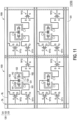
- FIG. 11 is a schematic partial top view of an electronic device according to another embodiment of the disclosure. Please refer to FIG. 1A and FIG. 11 at the same time.
- An electronic device 10i and a modulation unit 100i of this embodiment are substantially similar to the electronic device 10 and the modulation unit 100 of FIG. 1A and FIG. 1B , so the same and similar components in the two embodiments are not repeated here.
- the electronic device 10i and the modulation unit 100i of this embodiment are different from the electronic device 10 and the modulation unit 100 in that the electronic device 10i of this embodiment further includes multiple scanning lines SL, multiple signal lines DL, and a modulation module 11i, and each modulation unit 100i further includes multiple transistors TFT1, TFT2, and TFT3.
- the modulation module 11i includes multiple modulation units 100i arranged in an array, wherein the modulation units 100i disposed in the modulation module 11i may be the same or different.
- the scanning lines SL and the signal lines DL are respectively disposed on the substrate 101.
- the scanning lines SL and the signal lines DL are interleaved with each other to define the modulation units 100i arranged in an array.
- the scanning lines SL may be electrically connected to gates G in the transistor TFT1, the transistor TFT2, and the transistor TFT3, the signal lines DL may be electrically connected to sources S in the transistor TFT1, the transistor TFT2, and the transistor TFT3, and the first conductive layer pattern 120 may be electrically connected to drains D in the transistor TFT1, the transistor TFT2, and the transistor TFT3.
- the transistor TFT1, the transistor TFT2, and the transistor TFT3 may be respectively electrically connected to the first signal line 151, the second signal line 152, and the third signal line 153 to independently regulate each modulation unit 100i.
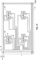
- FIG. 12 is a schematic partial top view of an electronic device according to another embodiment of the disclosure. Please refer to FIG. 1A and FIG. 12 at the same time.
- An electronic device 10j and a modulation unit 100j of this embodiment are substantially similar to the electronic device 10 and the modulation unit 100 of FIG. 1A and FIG. 1B , so the same and similar components in the two embodiments are not repeated here.
- the electronic device 10j and the modulation unit 100j of this embodiment are different from the electronic device 10 and the modulation unit 100 in that the electronic device 10j of this embodiment further includes multiple scanning lines SL, multiple signal lines DL, a chip C, and a modulation module 11j.
- the modulation module 11j includes multiple modulation units 100j arranged in an array, wherein the modulation units 100j disposed in the modulation module 11j may be the same or different.
- the scanning lines SL and the signal lines DL are respectively disposed on the substrate 101.
- the scanning lines SL and the signal lines DL are interleaved with each other to define the modulation units 100j.
- the chip C may be, for example, a chip packaged by an IC or multiple TFT elements, or a die formed by multiple TFT elements.
- the chip C may include a driving circuit. Since the chip C may be respectively electrically connected to the first part 121, the second part 122, and the third part 123 in each modulation unit 100j through the first signal line 151, the second signal line 152, and the third signal line 153, the chip C may simultaneously drive multiple modulation units 100j.
- FIG. 13 is a schematic partial top view of an electronic device according to another embodiment of the disclosure. Please refer to FIG. 1A and FIG. 13 at the same time.
- a modulation unit 100k of this embodiment is substantially similar to the modulation unit 100 of FIG. 1A , so the same and similar components in the two embodiments are not repeated here.
- the modulation unit 100k of this embodiment is different from the modulation unit 100 in that in each modulation unit 100k of this embodiment, a first conductive layer pattern 120k further includes a fourth part 124k, and a second electronic element 142k has 3 pads (not shown).
- the pattern of the first part 121, the pattern of the second part 122, the pattern of the third part 123, and the pattern of the fourth part 124 are separated from each other, and the pattern of the first part 121, the pattern of the second part 122, and the pattern of the third part 123 may be roughly formed into a hollow square shape, but not limited thereto.
- the pattern of the first part 121 may be regarded as L-shaped
- the pattern of the second part 122 may be regarded as a pattern composed of multiple separate solid square shapes
- the pattern of the third part 123 may be regarded as a solid square shape
- the pattern of the fourth part 124 may be regarded as a solid square shape, but not limited thereto.
- the bonding pad 161 and the bonding pad 162 are respectively disposed on the first part 121, the bonding pad 163 is disposed on the second part 122, the bonding pad 164 is disposed on the third part 123, and the bonding pad 165 is disposed on the fourth part 124.
- the first electronic element 141 may be bonded to the first conductive layer pattern 120k through the bonding pad 161 and the bonding pad 163, and the second electronic element 142k having 3 pads may be bonded to the first conductive layer pattern 120k through the bonding pad 162, the bonding pad 164, and the bonding pad 165.
- the first signal line 151 may contact and be electrically connected to the first part 121
- the second signal line 152 may respectively contact and be electrically connected to the second part 122 and the third part 123
- the third signal line 153 may contact and be electrically connected to the fourth part 124k.
- the first signal line 151 may provide the first voltage V1 to the first electronic element 141
- the second signal line 152 may provide the second voltage V2 to the first electronic element 141.
- the first signal line 151 may also provide the first voltage V1 to the second electronic element 142k
- the second signal line 152 may also provide the second voltage V2 to the second electronic element 142k
- the third signal line 153 may provide the third voltage V3 to the second electronic element 142k.
- FIG. 14 is a schematic partial top view of an electronic device according to another embodiment of the disclosure. Please refer to FIG. 1A and FIG. 14 at the same time.
- a modulation unit 100m of this embodiment is substantially similar to the modulation unit 100 of FIG. 1A , so the same and similar components in the two embodiments are not repeated here.
- the modulation unit 100m in this embodiment is different from the modulation unit 100 in that in each modulation unit 100m of this embodiment, a first conductive layer pattern 120m further includes an opening region 129.
- the pattern of the first part 121, the pattern of the second part 122, and the pattern of the third part 123 are separated from each other, and the pattern of the first part 121 and the pattern of the third part 123 are disposed in the hollow of the pattern of the second part 122, but not limited thereto.
- the pattern of the first part 121 may be regarded as a hollow semicircular shape
- the pattern of the second part 122 may be regarded as a hollow square shape
- the pattern of the third part 123 may be regarded as a hollow semicircular shape, but not limited thereto.
- the opening region 129 is a region exposed by the first part 121, the second part 122, and the third part 123 of the first conductive layer pattern 120m.
- the sum of the area of the first part 121, the area of the second part 122, and the area of the third part 123 is greater than the area of the opening region 129.
- the bonding pad 161 and the bonding pad 162 are respectively disposed on the second part 122, the bonding pad 163 is disposed on the third part 123, and the bonding pad 164 is disposed on the first part 121.
- the first electronic element 141 may be bonded to the first conductive layer pattern 120m through the bonding pad 161 and the bonding pad 163, and the second electronic element 142 may be bonded to the first conductive layer pattern 120m through the bonding pad 162 and the bonding pad 164.
- the first signal line 151 may contact and be electrically connected to the first part 121
- the second signal line 152 may contact and be electrically connected to the second part 122
- the third signal line 153 may contact and be electrically connected to the third part 123.
- the second signal line 152 may provide the second voltage V2 to the first electronic element 141
- the third signal line 153 may provide the third voltage V3 to the first electronic element 141.
- the first signal line 151 may provide the first voltage V1 to the second electronic element 142
- the second signal line 152 may also provide the second voltage V2 to the second electronic element 142.
- FIG. 15 to FIG. 17 are schematic partial top views of an electronic device according to multiple embodiments of the disclosure. Please refer to FIG. 1A and FIG. 15 to FIG. 17 at the same time.
- Modulation units 100n, 100p, and 100q of this embodiment are substantially similar to the modulation unit 100 of FIG. 1A , so the same and similar components in the two embodiments are not repeated here.
- the differences between the modulation units 100n, 100p, and 100q of this embodiment and the modulation unit 100 are as follows.
- the shapes of the contours of a first signal line 151n, a second signal line 152n, and a third signal line 153n may be arc-shaped wavy structures, so that the first signal line 151n, the second signal line 152n, and the third signal line 153n do not need to be additionally provided with radio frequency chokes.
- the shapes of the contours of a first signal line 151p, a second signal line 152p, and a third signal line 153p may be rectangular wavy structures, so that the first signal line 151p, the second signal line 152p, and the third signal line 153p do not need to be additionally provided with radio frequency chokes.
- the shapes of the contours of a first signal line 151q, a second signal line 152q, and a third signal line 153q may be loop structures, so that the first signal line 151q, the second signal line 152q, and the third signal line 153q do not need to be additionally provided with radio frequency chokes.
- the modulation unit may modulate the intensity, the bandwidth, or the phase of the received signal (for example, the electromagnetic wave signal or the light signal). Then, since the first electronic element and the second electronic element may share the third voltage of the third signal line, the overall circuit configuration of the modulation unit may be relatively simple and not complicated.
- the regulated first electronic element and second electronic element may respectively display various different characteristics, thereby increasing the modulable factor of the modulation unit or increasing the selection of the first electronic element and the second electronic element.
Landscapes
- Engineering & Computer Science (AREA)
- Computer Networks & Wireless Communication (AREA)
- Signal Processing (AREA)
- Structure Of Printed Boards (AREA)
- Semiconductor Integrated Circuits (AREA)
- Amplifiers (AREA)
- Optical Modulation, Optical Deflection, Nonlinear Optics, Optical Demodulation, Optical Logic Elements (AREA)
Abstract
Description
- The disclosure relates to an electronic device, and in particular to an electronic device having a modulation unit capable of modulating a phase, a bandwidth, an intensity, or a polarization state of an electromagnetic wave.
- Electronic devices or splicing electronic devices have been widely used in mobile phones, televisions, monitors, tablet computers, car displays, wearable devices, and desktop computers. With the vigorous development of electronic devices, the quality requirements for electronic devices are increasing, and such electronic products can often be used as electronic modulation devices at the same time, for example, as antenna devices that can modulate electromagnetic waves. However, the existing antenna devices still do not meet the requirements of consumers in all aspects.
- The disclosure provides an electronic device having a modulation unit capable of modulating a phase, a bandwidth, an intensity, or a polarization state of an electromagnetic wave.
- According to an embodiment of the disclosure, the electronic device includes a substrate and multiple modulation units. The modulation units are disposed on the substrate. Each modulation unit includes a first electronic element, a second electronic element, a first signal line, a second signal line, and a third signal line. The first signal line provides a first voltage to the first electronic element. The second signal line provides a second voltage to the second electronic element. The third signal line provides a third voltage to the first electronic element and/or the second electronic element. The first voltage is different from the second voltage, and the third voltage is different from the first voltage and/or the second voltage.
- The drawings are included to provide a further understanding of the disclosure, and the drawings are incorporated into the specification and constitute a part of the specification. The drawings illustrate embodiments of the disclosure and serve to explain principles of the disclosure together with the description.
-
FIG. 1A is a schematic partial top view of an electronic device according to an embodiment of the disclosure. -
FIG. 1B is a schematic cross-sectional view of the electronic device ofFIG. 1A along a section line I-I'. -
FIG. 2A is a schematic partial top view of an electronic device according to another embodiment of the disclosure. -
FIG. 2B is a schematic cross-sectional view of the electronic device ofFIG. 2A along a section line II-II'. -
FIG. 3A is a schematic partial top view of an electronic device according to another embodiment of the disclosure. -
FIG. 3B is a schematic cross-sectional view of the electronic device ofFIG. 3A along a section line III-III'. -
FIG. 4A is a schematic partial top view of an electronic device according to another embodiment of the disclosure. -
FIG. 4B is a schematic cross-sectional view of the electronic device ofFIG. 4A along a section line IV-IV'. -
FIG. 5 is a schematic partial top view of an electronic device according to another embodiment of the disclosure. -
FIG. 6 is a schematic partial top view of an electronic device according to another embodiment of the disclosure. -
FIG. 7 is a schematic partial top view of an electronic device according to another embodiment of the disclosure. -
FIG. 8 is a schematic partial top view of an electronic device according to another embodiment of the disclosure. -
FIG. 9 is a schematic partial top view of an electronic device according to another embodiment of the disclosure. -
FIG. 10 is a functional schematic view of an electronic device according to another embodiment of the disclosure. -
FIG. 11 is a schematic partial top view of an electronic device according to another embodiment of the disclosure. -
FIG. 12 is a schematic partial top view of an electronic device according to another embodiment of the disclosure. -
FIG. 13 is a schematic partial top view of an electronic device according to another embodiment of the disclosure. -
FIG. 14 is a schematic partial top view of an electronic device according to another embodiment of the disclosure. -
FIG. 15 to FIG. 17 are schematic partial top views of an electronic device according to multiple embodiments of the disclosure. - The disclosure may be understood by referring to the following detailed description in conjunction with the drawings. It should be noted that in order to facilitate understanding by the reader and the simplicity of the drawings, multiple drawings in the disclosure only depict a part of an electronic device, and specific elements in the drawings are not drawn according to actual scale. In addition, the number and the size of each element in the drawings are for illustration only and are not intended to limit the scope of the disclosure.
- In the following description and claims, words such as "comprising" and "including" are open-ended words, so the words should be interpreted as meaning "comprising but not limited to...".
- It will be understood that when an element or a film layer is referred to as being "on" or "connected to" another element or film layer, the element or the film layer may be directly on the other element or film layer or directly connected to the other element or film layer, or there may be an intervening element or film layer between the two (indirect case). In contrast, when an element is referred to as being "directly on" or "directly connected to" another element or film layer, there is no intervening element or film layer between the two.
- Although the terms "first", "second", "third"... may be used to describe various constituent elements, the constituent elements are not limited by the terms. The terms are only used to distinguish a single constituent element from other constituent elements in the specification. The same terms may not be used in the claims, but replaced by first, second, third... according to the order in which the elements are declared in the claims. Therefore, a first constituent element in the following specification may be a second constituent element in the claims.
- In the text, the terms "about", "approximately", "substantially", and "roughly" generally mean within 0.5%, 1%, 2%, 3%, 5%, or 10% of a given value or range. The number given here is an approximate number, that is, the meaning of "about", "approximately", "substantially", or "roughly" may still be implied without the specific description of "about", "approximately", "substantially", and "roughly".
- In some embodiments of the disclosure, terms related to bonding and connection such as "connection" and "interconnection" may mean that two structures are in direct contact or may also mean that two structures are not in direct contact, wherein there is another structure disposed between the two structures, unless otherwise defined. Also, the terms related to bonding and connection may also include the case where the two structures are both movable or the two structures are both fixed. Furthermore, the term "coupling" includes any direct and indirect means of electrical connection.
- The electronic device may include a display device, an antenna device (for example, a liquid crystal antenna), a sensing device, a light emitting device, a touch device, or a splicing device, but not limited thereto. The electronic device may include a bendable or flexible electronic device. The appearance of the electronic device may be rectangular, circular, polygonal, a shape with curved edges, or other suitable shapes. The display device may, for example, include a light emitting diode (LED), liquid crystal, fluorescence, phosphor, quantum dot (QD), other suitable materials, or a combination of the foregoing, but not limited thereto. The light emitting diode may include, for example, an organic light emitting diode (OLED), an inorganic light emitting diode, a mini LED, a micro LED, a QDLED, other suitable materials, or any combination of the foregoing, but not limited thereto. The display device may also include, for example, a splicing display device, but not limited thereto. The antenna device may be, for example, a liquid crystal antenna, but not limited thereto. The antenna device may include, for example, an antenna splicing device, but not limited thereto. It should be noted that the electronic device may be any combination of the foregoing, but not limited thereto. In addition, the appearance of the electronic device may be rectangular, circular, polygonal, a shape with curved edges, or other suitable shapes. The electronic device may have a peripheral system such as a driving system, a control system, a light source system, and a shelf system to support the display device, the antenna device, or the splicing device. The disclosure will be described below with the electronic device, but the disclosure is not limited thereto.
- It should be noted that in the following embodiments, features in several different embodiments may be replaced, recombined, and mixed to complete other embodiments without departing from the spirit of the disclosure. As long as the features between various embodiments do not violate the spirit of the invention or conflict with each other, the features may be mixed and matched arbitrarily.
- Reference will now be made in detail to the exemplary embodiments of the disclosure, examples of which are illustrated in the drawings. Wherever possible, the same reference numerals are used in the drawings and the description to refer to the same or similar parts.
-
FIG. 1A is a schematic partial top view of an electronic device according to an embodiment of the disclosure.FIG. 1B is a schematic cross-sectional view of the electronic device ofFIG. 1A along a section line I-I'. For the clarity of the drawings and the convenience of description,FIG. 1A omits to show several elements in anelectronic device 10. - Please refer to
FIG. 1A and FIG. 1B at the same time. Theelectronic device 10 of this embodiment includes asubstrate 101 andmultiple modulation units 100. Themodulation units 100 are disposed on thesubstrate 101 and are used to modulate an intensity, a bandwidth, or a phase of a received electromagnetic wave signal (or light signal, but not limited thereto). Specifically, eachmodulation unit 100 includes a firstconductive layer pattern 120, afirst insulation layer 130, a firstelectronic element 141, a secondelectronic element 142, afirst signal line 151, asecond signal line 152, and athird signal line 153. Thesubstrate 101 may include a hard substrate, a soft substrate, or a combination of the foregoing. For example, the material of thesubstrate 101 may include glass, quartz, silicon wafer, sapphire, III-V semiconductor material, ceramics, polycarbonate (PC), polyimide (PI), polyethylene terephthalate (PET), other suitable substrate materials, or a combination of the foregoing, but not limited thereto. In some embodiments, thesubstrate 101 may be a printed circuit board. - In this embodiment, a conductive layer including the first
conductive layer pattern 120 is disposed on thesubstrate 101. The firstconductive layer pattern 120 includes afirst part 121, asecond part 122, and athird part 123. Thefirst part 121, thesecond part 122, and thethird part 123 are separated from each other. Thethird part 123 is located between thefirst part 121 and thesecond part 122. In this embodiment, the firstconductive layer pattern 120 may resonate with the received electromagnetic wave signal (or light signal). The material of the firstconductive layer pattern 120 may include copper, aluminum, silver, gold, indium tin oxide (ITO), metal alloy, other suitable conductive materials, or a combination of the foregoing materials, but not limited thereto. - In this embodiment, in the schematic top view of the modulation unit 100 (as shown in
FIG. 1A ), the pattern of the firstconductive layer pattern 120 may include the pattern of thefirst part 121, the pattern of thesecond part 122, and the pattern of thethird part 123. The pattern of thefirst part 121 and the pattern of thesecond part 122 may be regarded as E-shaped, and the pattern of thethird part 123 may be regarded as a solid square shape, but not limited thereto. The pattern of thefirst part 121, the pattern of thesecond part 122, and the pattern of thethird part 123 are separated from each other. The pattern of thefirst part 121 and the pattern of thesecond part 122 may surround the pattern of thethird part 123, and the pattern of thefirst part 121 and the pattern of thesecond part 122 may be disposed on two sides of the pattern of thethird part 123 in a mirroring manner, but not limited thereto. - In this embodiment, the first part of the insulation layer, that is, the
first insulation layer 130 is disposed on the firstconductive layer pattern 120 to cover a part of the firstconductive layer pattern 120 and cover a part of thesubstrate 101 exposed by an opening between the firstconductive layer patterns 120. Thefirst insulation layer 1 30 may expose another part of the firstconductive layer pattern 120 for disposing abonding pad 161, abonding pad 162, abonding pad 163, and abonding pad 164. In this embodiment, thefirst insulation layer 130 may be a single-layer or multi-layer structure, and the material of thefirst insulation layer 130 may include a polymer thin film, silicon nitride, silicon oxide, silicon oxynitride, or a combination of the foregoing, but not limited thereto. - In this embodiment, each
modulation unit 100 further includes abonding pad 161, abonding pad 162, abonding pad 163, and abonding pad 164, wherein thebonding pad 161 and thebonding pad 163 are respectively disposed between the firstconductive layer pattern 120 and the firstelectronic element 141, and thebonding pad 162 and thebonding pad 164 are respectively disposed between the firstconductive layer pattern 120 and the secondelectronic element 142. Thebonding pad 161 is disposed on thefirst part 121 of the firstconductive layer pattern 120 to contact thefirst part 121. Thebonding pad 162 is disposed on thesecond part 122 of the firstconductive layer pattern 120 to contact thesecond part 122. Thebonding pad 163 and thebonding pad 164 are respectively disposed on thethird part 123 of the firstconductive layer pattern 120 to contact thethird part 123. In this embodiment, the materials of thebonding pad 161, thebonding pad 162, thebonding pad 163, and thebonding pad 164 may include copper, aluminum, silver, gold, indium tin oxide, metal alloys (for example, electroless nickel immersion gold (ENIG)), other suitable conductive materials, or a combination of the foregoing materials, but not limited thereto. - In this embodiment, each
modulation unit 100 further includesmultiple solder balls bonding pad 161, thebonding pad 162, thebonding pad 163, and thebonding pad 164. Thesolder ball 165 may contact thebonding pad 161, thesolder ball 166 may contact thebonding pad 162, thesolder ball 167 may contact thebonding pad 163, and thesolder ball 168 may contact thebonding pad 164. - In this embodiment, the first
electronic element 141 and the secondelectronic element 142 are disposed on thefirst signal line 151, thesecond signal line 152, and thethird signal line 153. The firstelectronic element 141 has apad 141a and apad 141b, and the secondelectronic element 142 has apad 142a and apad 142b. The firstelectronic element 141 may be bonded to thebonding pad 161 through thepad 141a and thesolder ball 165, and may be bonded to thebonding pad 163 through thepad 141b and thesolder ball 167. The secondelectronic element 142 may be bonded to thebonding pad 162 through thepad 142a and thesolder ball 166, and may be bonded to thebonding pad 164 through thepad 142b and thesolder ball 168. In other words, the firstelectronic element 141 may be bonded to the firstconductive layer pattern 120 through thebonding pad 161 and thebonding pad 163, and the secondelectronic element 142 may be bonded to the firstconductive layer pattern 120 through thebonding pad 162 and thebonding pad 164. - In this embodiment, the first
electronic element 141 and the secondelectronic element 142 may have the characteristic of being sensitive to external stimuli, and the firstelectronic element 141 and the secondelectronic element 142 may be regulated by the external stimuli to change their own characteristics, wherein the external stimulus is, for example, voltage, current, temperature, etc., and their own characteristic is, for example, a capacitance value or a resistance value, but not limited thereto. In this embodiment, the firstelectronic element 141 and the secondelectronic element 142 may include, for example, capacitors, inductors, or resistors, but not limited thereto. For example, when the firstelectronic element 141 and/or the secondelectronic element 142 are capacitors, themodulation unit 100 may regulate the capacitors by applying voltages to change the capacitance values of the capacitors. - In addition, in some embodiments, the first
electronic element 141 and the secondelectronic element 142 may also be, for example, electronic elements containing materials sensitive to external stimuli, electronic elements containing elements sensitive to external stimuli, or electronic elements containing structures sensitive to external stimuli. The material sensitive to external stimuli may be, for example, liquid crystal, vanadium oxide, etc., the element sensitive to external stimuli may be, for example, a PIN diode, a varactor diode, a Schottky diode, a Gunn diode, etc., the structure sensitive to external stimuli may be, for example, micro electro mechanical systems (MEMS), etc., but not limited thereto. - In addition, in some embodiments, the first
electronic element 141 and the secondelectronic element 142 may also be different electronic elements. For example, the firstelectronic element 141 may be an inductor and the secondelectronic element 142 may be a capacitor or the firstelectronic element 141 may be a switching element and the secondelectronic element 142 may be a diode. Therefore, one modulation element may modulate two different characteristics. - In this embodiment, the
first signal line 151, thesecond signal line 152, and thethird signal line 153 are respectively disposed on thesubstrate 101 and thefirst insulation layer 130. Thefirst signal line 151, thesecond signal line 152, and thethird signal line 153 may be the same film layer as the firstconductive layer pattern 120, but not limited thereto. Thefirst signal line 151 may contact and be coupled to thefirst part 121 of the firstconductive layer pattern 120, thesecond signal line 152 may contact and be coupled to thesecond part 122 of the firstconductive layer pattern 120, and thethird signal line 153 may contact and be coupled to thethird part 123 of the firstconductive layer pattern 120. - In this embodiment, the
first signal line 151 has a first voltage V1, thesecond signal line 152 has a second voltage V2, and thethird signal line 153 has a third voltage V3. The first voltage V1, the second voltage V2, and the third voltage V3 are low frequency voltage signals, for example, the frequency range is 0 to 100 MHz. Thefirst signal line 151 may provide the first voltage V1 to the firstelectronic element 141 through thefirst part 121, thebonding pad 161, thesolder ball 165, and thepad 141a. Thesecond signal line 152 may provide the second voltage V2 to the secondelectronic element 142 through thesecond part 122, thebonding pad 162, thesolder ball 165, and thepad 142b. Thethird signal line 153 may provide the third voltage V3 to the firstelectronic element 141 through thethird part 123, thebonding pad 163, thesolder ball 165, and thepad 141b, and provide the third voltage V3 to the secondelectronic element 142 through thethird part 123, thebonding pad 164, thesolder ball 165, and thepad 142a. Therefore, in this embodiment, the firstelectronic element 141 may be regulated and the own characteristics of the firstelectronic element 141 may be changed using the third voltage V3 of thethird signal line 153 matched with the first voltage V1 of thefirst signal line 151 or the secondelectronic element 142 may be regulated and the own characteristics of the secondelectronic element 142 may be changed using the third voltage V3 of thethird signal line 153 matched with the second voltage V2 of thesecond signal line 152. In this way, themodulation unit 100 may modulate the phase, the intensity, the bandwidth, or the polarization state of the received electromagnetic wave signal (or light signal, but not limited thereto), and output the modulated electromagnetic wave signal (or light signal, but not limited thereto). - In addition, in this embodiment, a voltage difference (that is, a difference value between the first voltage V1 and the third voltage V3) in the first
electronic element 141 and a voltage difference (that is, a difference value between the first voltage V1 and the second voltage V2) in the secondelectronic element 142 may be independently regulated by thefirst signal line 151, thesecond signal line 152, and/or thethird signal line 153. In this embodiment, since the firstelectronic element 141 and the secondelectronic element 142 may share the third voltage V3 of thethird signal line 153, the overall circuit configuration of themodulation unit 100 can be relatively simple and not complicated. In this embodiment, since the first voltage V1 may be different from the second voltage V2, and the third voltage V3 may be different from the first voltage V1 and the second voltage V2, the regulated firstelectronic element 141 and secondelectronic element 142 may respectively display various different characteristics, thereby increasing the modulable factor of themodulation unit 100 or increasing the selection of the firstelectronic element 141 and the secondelectronic element 142. - In this embodiment, since the
first signal line 151, thesecond signal line 152, and thethird signal line 153 may be respectively electrically connected to the firstconductive layer pattern 120, eachmodulation unit 100 needs to be additionally provided with multiple radio frequency chokes 170 to block a high frequency signal or an alternating current voltage in the firstconductive layer pattern 120 from entering (or interfering with) thefirst signal line 151, thesecond signal line 152, and thethird signal line 153 with low frequency signals or direct current voltages. Specifically, the radio frequency chokes 170 are respectively disposed in thefirst signal line 151, thesecond signal line 152, and thethird signal line 153 to stabilize the first voltage V1, the second voltage V2, and the third voltage V3. - Although the first voltage V1, the second voltage V2, and the third voltage V3 in this embodiment are all different from each other, the disclosure is not limited thereto. In other words, in some embodiments, the voltages of any two of the first voltage, the second voltage, and the third voltage may be different.
- Although the
first signal line 151, thesecond signal line 152, and thethird signal line 153 in this embodiment may be the same film layer as the firstconductive layer pattern 120, the disclosure is not limited thereto. In other words, in some embodiments, the first signal line, the second signal line, and the third signal line may also be different film layers from the first conductive layer pattern, as shown inFIG. 2A, FIG. 2B ,FIG. 3A, and FIG. 3B . In some embodiments, one or two of the first signal line, the second signal line, and the third signal line may be the same film layer as the first conductive layer pattern, and the other one or the other two of the signal lines may be different film layers from the first conductive layer pattern, as shown inFIG. 6 . - In this embodiment, in the schematic top view of the modulation unit 100 (as shown in
FIG. 1A ), although the shapes of the contours of thefirst signal line 151, thesecond signal line 152, and thethird signal line 153 are straight lines, the disclosure is not limited thereto. In some embodiments, the shapes of the contours of the first signal line, the second signal line, and the third signal line may also be wavy structures or loop structures. - Other embodiments are listed below for illustration. It must be noted here that the following embodiments continue to use the reference numerals and some contents of the foregoing embodiment, wherein the same reference numeral is adopted to represent the same or similar elements, and the description of the same technical content is omitted. For the description of the omitted part, reference may be made to the foregoing embodiment, which will not be repeated in the following embodiments.
-
FIG. 2A is a schematic partial top view of an electronic device according to another embodiment.FIG. 2B is a schematic cross-sectional view of the electronic device ofFIG. 2A along a section line II-II'. Please refer toFIG. 1A, FIG. 1B ,FIG. 2A, and FIG. 2B at the same time. Amodulation unit 100a of this embodiment is substantially similar to themodulation unit 100 ofFIG. 1A to FIG. 1B , so the same and similar components in the two embodiments are not repeated here. Themodulation unit 100a of this embodiment is different from themodulation unit 100 in that eachmodulation unit 100a of this embodiment further includes asecond insulation layer 132 and a secondconductive layer pattern 180. - Specifically, please refer to
FIG. 2A and FIG. 2B . In this embodiment, a section of another insulation layer, that is, thesecond insulation layer 132 is disposed on thefirst insulation layer 130 to cover at least one part of thefirst insulation layer 130 and expose another part of thefirst insulation layer 130. Thesecond insulation layer 132 may be a single-layer or multi-layer structure, and the material of thesecond insulation layer 132 may include a polymer thin film, silicon nitride, silicon oxide, silicon oxynitride, or a combination of the foregoing, but not limited thereto. - In this embodiment, a
first signal line 151a, asecond signal line 152a, and athird signal line 153a are disposed on thefirst insulation layer 130 exposed by thesecond insulation layer 132, so that thefirst signal line 151a is physically separated from thefirst part 121, thesecond signal line 152a is physically separated from thesecond part 122, and thethird signal line 153a is physically separated from thethird part 123. The secondconductive layer pattern 180 is disposed on thefirst signal line 151a, thesecond signal line 152a, and thethird signal line 153a. In other words, the secondconductive layer pattern 180 may be disposed between asignal line 150 and anelectronic element 140, wherein thesignal line 150 includes thefirst signal line 151a, thesecond signal line 152a, and thethird signal line 153a, and theelectronic element 140 includes the firstelectronic element 141 and the secondelectronic element 142. The secondconductive layer pattern 180 includes afirst pad 181, asecond pad 182, and athird pad 183 that are separated from each other. Thefirst pad 181 may be disposed corresponding to thefirst part 121, thesecond pad 182 may be disposed corresponding to thesecond part 122, and thethird pad 183 may be disposed corresponding to thethird part 123. - In this embodiment, the
first signal line 151a may contact and be electrically connected to thefirst pad 181, thesecond signal line 152a may contact and be electrically connected to thesecond pad 182, and thethird signal line 153a may contact and be electrically connected to thethird pad 183. Thefirst pad 181 may be electrically connected to thefirst signal line 151a and the firstelectronic element 141, thesecond pad 182 may be electrically connected to thesecond signal line 152a and the secondelectronic element 142, and thethird pad 183 may be electrically connected to thethird signal line 153a and the firstelectronic element 141 and/or the secondelectronic element 142. - In this embodiment, since the high frequency signal or the alternating current voltage in the first
conductive layer pattern 120 will not enter (or interfere with) thefirst signal line 151a, thesecond signal line 152a, and thethird signal line 153a with low frequency signals or direct current voltages, eachmodulation unit 100a does not need to be additionally provided with multiple radio frequency chokes. - In this embodiment, since the first
conductive layer pattern 120 is indirectly electrically connected to the firstelectronic element 141 and the secondelectronic element 142, the firstelectronic element 141 and the secondelectronic element 142 need to regulate an electromagnetic wave signal (or a light signal, but not limited to) between the firstconductive layer patterns 120 through induction. - In this embodiment, a thickness T of the
first insulation layer 130 may be 100 angstroms (Å) to 10 micrometers (µm), wherein the thickness T is the minimum thickness of thefirst insulation layer 130 measured along a normal direction of thesubstrate 101. -
FIG. 3A is a schematic partial top view of an electronic device according to another embodiment of the disclosure.FIG. 3B is a schematic cross-sectional view of the electronic device ofFIG. 3A along a section line III-III'. Please refer toFIG. 2A, FIG. 2B ,FIG. 3A, and FIG. 3B at the same time. Amodulation unit 100b of this embodiment is substantially similar to themodulation unit 100a ofFIG. 2A and FIG. 2B , so the same and similar components in the two embodiments are not repeated here. Themodulation unit 100b of this embodiment is different from themodulation unit 100a in that eachmodulation unit 100b in this embodiment further includes aconductive hole 190. - Specifically, please refer to
FIG. 3A and FIG. 3B . In this embodiment, theconductive hole 190 may penetrate thefirst insulation layer 130 and electrically connect the secondconductive layer pattern 180 and the firstconductive layer pattern 120. Since thefirst signal line 151a, thesecond signal line 152a, and thethird signal line 153a may be electrically connected to the firstconductive layer pattern 120 through the secondconductive layer pattern 180 and theconductive hole 190, themodulation unit 100b of this embodiment needs to be additionally provided with multiple radio frequency chokes 170 in thefirst signal line 151a, thesecond signal line 152a, and thethird signal line 153a. - In addition, since the first
conductive layer pattern 120 may be electrically connected to the firstelectronic element 141 and the secondelectronic element 142 through theconductive hole 190 and the secondconductive layer pattern 180, themodulation unit 100b of this embodiment does not need to limit the thickness of thefirst insulation layer 130. -
FIG. 4A is a schematic partial top view of an electronic device according to another embodiment of the disclosure.FIG. 4B is a schematic cross-sectional view of the electronic device ofFIG. 4A along a section line IV-IV'. Please refer toFIG. 2A, FIG. 2B ,FIG. 4A, and FIG. 4B at the same time. Amodulation unit 100c of this embodiment is substantially similar to themodulation unit 100a ofFIG. 2A and FIG. 2B , so the same and similar components in the two embodiments are not repeated here. Themodulation unit 100c of this embodiment is different from themodulation unit 100a in that thefirst signal line 151a, thesecond signal line 152a, and thethird signal line 153a of this embodiment do not contact the secondconductive layer pattern 180. - Specifically, please refer to
FIG. 4A and FIG. 4B . In this embodiment, thefirst insulation layer 130 has multiple openings to expose thefirst part 121, thesecond part 122, and thethird part 123 of the firstconductive layer pattern 120. - In this embodiment, the
first signal line 151a, thesecond signal line 152a, and thethird signal line 153a are disposed on the firstconductive layer pattern 120 exposed by thefirst insulation layer 130, so that thefirst signal line 151a may contact thefirst part 121, thesecond signal line 152a may contact thesecond part 122, and thethird signal line 153a may contact thethird part 123. - In this embodiment, the second
conductive layer pattern 180 is disposed on the firstconductive layer pattern 120 exposed by thefirst insulation layer 130, so that thefirst pad 181 may contact thefirst part 121, thesecond pad 182 may contact thesecond part 122, and thethird pad 183 may contact thethird part 123. Thefirst pad 181 does not contact thefirst signal line 151a, thesecond pad 182 does not contact thesecond signal line 152a, and thethird pad 183 does not contact thethird signal line 153a. Thefirst pad 181 may be electrically connected to thefirst signal line 151a through thefirst part 121, thesecond pad 182 may be electrically connected to thesecond signal line 152a through thesecond part 122, and thethird pad 183 may be electrically connected to the third signal line through thethird part 123 153a. - The
second insulation layer 132 is disposed on thefirst insulation layer 130 to cover thefirst insulation layer 130, thefirst signal line 151a, thesecond signal line 152a, and thethird signal line 153a. Thesecond insulation layer 132 may also be disposed in a gap between thefirst pad 181 and thefirst signal line 151a, a gap between thesecond pad 182 and thesecond signal line 152a, and a gap between thethird pad 183 and thethird signal line 153a. -
FIG. 5 is a schematic partial top view of an electronic device according to another embodiment of the disclosure. Please refer toFIG. 1A andFIG. 5 at the same time. Amodulation unit 100d of this embodiment is substantially similar to themodulation unit 100 ofFIG. 1A , so the same and similar components in the two embodiments are not repeated here. Themodulation unit 100d of this embodiment is different from themodulation unit 100 in that in eachmodulation unit 100d of this embodiment, a pattern of a firstconductive layer pattern 120d may be roughly regarded as a hollow square shape. - Specifically, please refer to
FIG. 5 . In the schematic top view of themodulation unit 100d, the pattern of thefirst part 121 and the pattern of thesecond part 122 may be regarded as L-shaped, and the pattern of thethird part 123 may be regarded as C-shaped, but not limited thereto. The pattern of thefirst part 121, the pattern of thesecond part 122, and the pattern of thethird part 123 are separated from each other, and the pattern of thefirst part 121, the pattern of thesecond part 122, and the pattern of thethird part 123 may be roughly formed into a hollow square shape, but not limited thereto. In addition, in this embodiment, the firstelectronic element 141 and the secondelectronic element 142 are respectively disposed on two sides of the pattern of the firstconductive layer pattern 120d, but not limited thereto. -
FIG. 6 is a schematic partial top view of an electronic device according to another embodiment of the disclosure. Please refer toFIG. 2A andFIG. 6 at the same time. Amodulation unit 100e of this embodiment is substantially similar to themodulation unit 100 ofFIG. 1A , so the same and similar components in the two embodiments are not repeated here. Themodulation unit 100e of this embodiment is different from themodulation unit 100 in that in eachmodulation unit 100e of this embodiment, a first electronic element 141d and a second electronic element 142d both have 3 pads (not shown). - Specifically, please refer to
FIG. 6 . In the schematic top view of themodulation unit 100e, the firstconductive layer pattern 120e includes thefirst part 121, thesecond part 122, and thethird part 123. The pattern of thefirst part 121 and the pattern of thesecond part 122 may be regarded as a solid square shape, and the pattern of thethird part 123 may be regarded asshaped, but not limited thereto. The pattern of the
first part 121, the pattern of thesecond part 122, and the pattern of thethird part 123 are separated from each other, and the pattern of thefirst part 121, the pattern of thesecond part 122, and the pattern of thethird part 123 may be roughly formed into ashape (that is, the pattern of the first
conductive layer pattern 120e may be roughly regarded as theshape), but not limited thereto. In addition, in this embodiment, the first electronic element 141d and the second electronic element 142d are respectively disposed on two sides of the pattern of the first
conductive layer pattern 120e, but not limited thereto. - In this embodiment, the second
conductive layer pattern 180d is disposed on the firstconductive layer pattern 120e and includes thefirst pad 181 and thesecond pad 182 separated from each other. Thefirst pad 181 may be disposed corresponding to thefirst part 121, and thesecond pad 182 may be disposed corresponding to thesecond part 122. Thebonding pad 161, thebonding pad 162, thebonding pad 163, and thebonding pad 164 are respectively disposed on thethird part 123 of the firstconductive layer pattern 120e to contact thethird part 123. The firstelectronic element 141 having 3 pads may be bonded to the firstconductive layer pattern 120e through thebonding pad 161, thefirst pad 181, and thebonding pad 163, and the secondelectronic element 142 having 3 pads may be bonded to the firstconductive layer pattern 120e through thebonding pad 162, thesecond pad 182, and thebonding pad 164. - In this embodiment, since the
third signal line 153 may contact and be electrically connected to thethird part 123 of the firstconductive layer pattern 120e, thethird signal line 153 needs to be additionally provided with theradio frequency choke 170. In addition, the first signal line 151d electrically connected to thefirst pad 181 and thesecond signal line 152d electrically connected to thesecond pad 182 do not need to be additionally provided with any radio frequency choke. -
FIG. 7 is a schematic partial top view of an electronic device according to another embodiment of the disclosure. Please refer toFIG. 1A andFIG. 7 at the same time. Amodulation unit 100f of this embodiment is substantially similar to themodulation unit 100 ofFIG. 1A , so the same and similar components in the two embodiments are not repeated here. Themodulation unit 100f of this embodiment is different from themodulation unit 100 in that eachmodulation unit 100f of this embodiment further includes afourth signal line 154, and a firstconductive layer pattern 120f further includes afourth part 124, afifth part 125, afifth part 126, afifth part 127, and afifth part 128. - Specifically, please refer to
FIG. 7 . In this embodiment, thefirst part 121, thesecond part 122, thethird part 123, thefourth part 124, thefifth part 125, thefifth part 126, thefifth part 127, and thefifth part 128 are separated from each other. Thefirst part 121, thesecond part 122, thethird part 123, and thefourth part 124 are disposed in the middle of the firstconductive layer pattern 120f, and thefifth part 125, thefifth part 126, thefifth part 127, and thefifth part 128 are disposed at the periphery of the firstconductive layer pattern 120f. The patterns of thefirst part 121, thesecond part 122, thethird part 123, thefourth part 124, thefifth part 125, thefifth part 126, thefifth part 127, and thefifth part 128 may be roughly formed into ashape (that is, the pattern of the first
conductive layer pattern 120f may be roughly regarded as theshape), but not limited thereto.
- In this embodiment, the
bonding pad 161 is disposed on thefirst part 121, thebonding pad 162 is disposed on thesecond part 122, thebonding pad 163 is disposed on thethird part 123, and thebonding pad 164 is disposed on thefourth part 124. The firstelectronic element 141 may be bonded to the firstconductive layer pattern 120f through thebonding pad 161 and thebonding pad 163, and the secondelectronic element 142 may be bonded to the firstconductive layer pattern 120f through thebonding pad 162 and thebonding pad 164. - In this embodiment, the
first signal line 151 may contact and be electrically connected to thefirst part 121, thesecond signal line 152 may contact and be electrically connected to thesecond part 122, thethird signal line 153 may contact and be electrically connected to thethird part 123, and thefourth signal line 154 may contact and be electrically connected to thefourth part 124. Thefirst signal line 151 may provide the first voltage V1 to the firstelectronic element 141, and thethird signal line 153 may provide the third voltage V3 to the firstelectronic element 141. Thesecond signal line 152 may provide the second voltage V2 to the secondelectronic element 142, and thefourth signal line 154 may provide a fourth voltage V4 to the secondelectronic element 142. -
FIG. 8 is a schematic partial top view of an electronic device according to another embodiment of the disclosure. Please refer toFIG. 1A andFIG. 8 at the same time. An electronic device 10g and a modulation unit 100g of this embodiment are substantially similar to theelectronic device 10 and themodulation unit 100 ofFIG. 1A and FIG. 1B , so the same and similar components in the two embodiments are repeated here. The electronic device 10g and the modulation unit 100g of this embodiment are different from theelectronic device 10 and themodulation unit 100 in that the electronic device 10g of this embodiment further includes multiple scanning lines SL, multiple signal lines DL, and amodulation module 11, and each modulation unit 100g further includes a chip C. - Specifically, please refer to
FIG. 8 . Themodulation module 11 includes multiple modulation units 100g arranged in an array, wherein the modulation units 100g disposed in themodulation module 11 may be the same or different. The scanning lines SL and the signal lines DL are respectively disposed on thesubstrate 101. The scanning lines SL and the signal lines DL are interleaved with each other to define the modulation units 100g arranged in an array. - In this embodiment, since the scanning lines SL may be electrically connected to the chip C, the signal lines DL may be electrically connected to the chip C, and the
first part 121, thesecond part 122, and thethird part 123 in the firstconductive layer pattern 120 may be respectively electrically connected to the chip C through thefirst signal line 151, thesecond signal line 152, and thethird signal line 153, the chip C may independently regulate each modulation unit 100g. In this embodiment, the chip C may be, for example, a chip packaged by an integrated circuit (IC) or multiple thin film transistor (TFT) elements, or a die formed by multiple TFT elements. The chip C includes a driving circuit, and the driving circuit may be respectively electrically connected to thefirst signal line 151, thesecond signal line 152, and thethird signal line 153. -
FIG. 9 is a schematic partial top view of an electronic device according to another embodiment of the disclosure. Please refer toFIG. 8 andFIG. 9 at the same time. Anelectronic device 10h of this embodiment is substantially similar to the electronic device 10g ofFIG. 8 , so the same and similar components in the two embodiments are not repeated here. Theelectronic device 10h in this embodiment is different from the electronic device 10g in that theelectronic device 10h in this embodiment further includes anemission source 12. - Specifically, please refer to
FIG. 9 . In this embodiment, theemission source 12 is configured to emit a signal EM (for example, an electromagnetic wave signal or a light signal). The signal EM (for example, the electromagnetic wave signal or the light signal) may propagate in, for example, a free space in any direction, but not limited thereto. In some embodiments, the signal EM (for example, the electromagnetic wave signal or the light signal) may also propagate in a wave-guided structure (not shown), wherein the wave-guided structure is, for example, a transmission line, a dielectric-filled waveguide, or a gas-filled waveguide, but not limited thereto. - In this embodiment, when each
modulation unit 100h in themodulation module 11 receives the signal EM (for example, the electromagnetic wave signal or the light signal) emitted by theemission source 12, themodulation module 11 may regulate the phase, the amplitude, or the polarization state of the signal EM (for example, the electromagnetic wave signal or the light signal) incident to eachmodulation unit 100h, so that eachmodulation unit 100h outputs the signal EM (for example, the electromagnetic wave signal or the light signal) to the same direction (that is, a first direction D1 or a second direction D2), but not limited thereto. In some embodiments, after themodulation module 11 regulates the phase of the signal EM (for example, the electromagnetic wave signal or the light signal) incident to eachmodulation unit 100h, eachmodulation unit 100h may also output the signal EM (for example, the electromagnetic wave signal or the light signal) to the same location (not shown). - In this embodiment, the
electronic device 10h may be applied to an antenna device, a display device for images, or a 5G millimeter-wave amplifier, but not limited thereto. - In addition, although the
modulation module 11 in this embodiment is disposed outside theemission source 12 to regulate the phase of the signal EM (for example, the electromagnetic wave signal or the light signal) emitted by theemission source 12, the disclosure does not limit the configuration location of themodulation module 11. In some embodiments, a modulation module may be disposed in an emission source to regulate a phase of a signal (for example, an electromagnetic wave signal or a light signal) before emitting the signal, as shown inFIG. 10 . -
FIG. 10 is a functional schematic view of an electronic device according to another embodiment of the disclosure. - Please refer to
FIG. 10 . Anelectronic device 20 of this embodiment may be regarded as an antenna device and includes abaseband circuit 21 and a phase array antenna 22. Specifically, the phase array antenna 22 includesmultiple antennas 200, and eachantenna 200 includes aconverter 220, aconverter 230, anintermediate frequency circuit 240 and ahigh frequency circuit 260. Theintermediate frequency circuit 240 includes afilter 241, anamplifier 242, amixer 243, alocal oscillator 244, and anamplifier 245. Thehigh frequency circuit 260 includes amixer 261, aphase shifter 262, apower amplifier 263, adiplexer 264, anantenna unit 265, and alow noise amplifier 266. - In this embodiment, when the
electronic device 20 emits a signal, thebaseband circuit 21 first converts the signal to theintermediate frequency circuit 240 through theconverter 220, the signal is then transmitted to thehigh frequency circuit 260 through thefilter 241, theamplifier 242, themixer 243, and thelocal oscillator 244 in theintermediate frequency circuit 240, then through themixer 261, thephase shifter 262, thepower amplifier 263, and thediplexer 264 in thehigh frequency circuit 260, and an electromagnetic wave signal is finally emitted to the outside through theantenna unit 265. On the contrary, when theelectronic device 20 receives a signal, theantenna unit 265 is first used to receive an electromagnetic wave signal from the outside, and the signal is then transmitted to thebaseband circuit 21 sequentially through thehigh frequency circuit 260, theintermediate frequency circuit 240, and theconverter 230. A modulation module (not shown) or a modulation unit (not shown) may be disposed in theantenna unit 265 to regulate the phase, the bandwidth, the intensity, or the polarization state of the electromagnetic wave signal before emitting the electromagnetic wave signal. -
FIG. 11 is a schematic partial top view of an electronic device according to another embodiment of the disclosure. Please refer toFIG. 1A andFIG. 11 at the same time. Anelectronic device 10i and amodulation unit 100i of this embodiment are substantially similar to theelectronic device 10 and themodulation unit 100 ofFIG. 1A and FIG. 1B , so the same and similar components in the two embodiments are not repeated here. Theelectronic device 10i and themodulation unit 100i of this embodiment are different from theelectronic device 10 and themodulation unit 100 in that theelectronic device 10i of this embodiment further includes multiple scanning lines SL, multiple signal lines DL, and a modulation module 11i, and eachmodulation unit 100i further includes multiple transistors TFT1, TFT2, and TFT3. - Specifically, please refer to
FIG. 11 . The modulation module 11i includesmultiple modulation units 100i arranged in an array, wherein themodulation units 100i disposed in the modulation module 11i may be the same or different. The scanning lines SL and the signal lines DL are respectively disposed on thesubstrate 101. The scanning lines SL and the signal lines DL are interleaved with each other to define themodulation units 100i arranged in an array. - In this embodiment, the scanning lines SL may be electrically connected to gates G in the transistor TFT1, the transistor TFT2, and the transistor TFT3, the signal lines DL may be electrically connected to sources S in the transistor TFT1, the transistor TFT2, and the transistor TFT3, and the first
conductive layer pattern 120 may be electrically connected to drains D in the transistor TFT1, the transistor TFT2, and the transistor TFT3. The transistor TFT1, the transistor TFT2, and the transistor TFT3 may be respectively electrically connected to thefirst signal line 151, thesecond signal line 152, and thethird signal line 153 to independently regulate eachmodulation unit 100i. -
FIG. 12 is a schematic partial top view of an electronic device according to another embodiment of the disclosure. Please refer toFIG. 1A andFIG. 12 at the same time. Anelectronic device 10j and amodulation unit 100j of this embodiment are substantially similar to theelectronic device 10 and themodulation unit 100 ofFIG. 1A and FIG. 1B , so the same and similar components in the two embodiments are not repeated here. Theelectronic device 10j and themodulation unit 100j of this embodiment are different from theelectronic device 10 and themodulation unit 100 in that theelectronic device 10j of this embodiment further includes multiple scanning lines SL, multiple signal lines DL, a chip C, and amodulation module 11j. - Specifically, please refer to
FIG. 12 . Themodulation module 11j includesmultiple modulation units 100j arranged in an array, wherein themodulation units 100j disposed in themodulation module 11j may be the same or different. The scanning lines SL and the signal lines DL are respectively disposed on thesubstrate 101. The scanning lines SL and the signal lines DL are interleaved with each other to define themodulation units 100j. - In this embodiment, the chip C may be, for example, a chip packaged by an IC or multiple TFT elements, or a die formed by multiple TFT elements. The chip C may include a driving circuit. Since the chip C may be respectively electrically connected to the
first part 121, thesecond part 122, and thethird part 123 in eachmodulation unit 100j through thefirst signal line 151, thesecond signal line 152, and thethird signal line 153, the chip C may simultaneously drivemultiple modulation units 100j. -
FIG. 13 is a schematic partial top view of an electronic device according to another embodiment of the disclosure. Please refer toFIG. 1A andFIG. 13 at the same time. Amodulation unit 100k of this embodiment is substantially similar to themodulation unit 100 ofFIG. 1A , so the same and similar components in the two embodiments are not repeated here. Themodulation unit 100k of this embodiment is different from themodulation unit 100 in that in eachmodulation unit 100k of this embodiment, a first conductive layer pattern 120k further includes a fourth part 124k, and a second electronic element 142k has 3 pads (not shown). - Specifically, please refer to
FIG. 13 . In this embodiment, the pattern of thefirst part 121, the pattern of thesecond part 122, the pattern of thethird part 123, and the pattern of thefourth part 124 are separated from each other, and the pattern of thefirst part 121, the pattern of thesecond part 122, and the pattern of thethird part 123 may be roughly formed into a hollow square shape, but not limited thereto. The pattern of thefirst part 121 may be regarded as L-shaped, the pattern of thesecond part 122 may be regarded as a pattern composed of multiple separate solid square shapes, the pattern of thethird part 123 may be regarded as a solid square shape, and the pattern of thefourth part 124 may be regarded as a solid square shape, but not limited thereto. - In this embodiment, the
bonding pad 161 and thebonding pad 162 are respectively disposed on thefirst part 121, thebonding pad 163 is disposed on thesecond part 122, thebonding pad 164 is disposed on thethird part 123, and thebonding pad 165 is disposed on thefourth part 124. The firstelectronic element 141 may be bonded to the first conductive layer pattern 120k through thebonding pad 161 and thebonding pad 163, and the second electronic element 142k having 3 pads may be bonded to the first conductive layer pattern 120k through thebonding pad 162, thebonding pad 164, and thebonding pad 165. - In this embodiment, the
first signal line 151 may contact and be electrically connected to thefirst part 121, thesecond signal line 152 may respectively contact and be electrically connected to thesecond part 122 and thethird part 123, and thethird signal line 153 may contact and be electrically connected to the fourth part 124k. Thefirst signal line 151 may provide the first voltage V1 to the firstelectronic element 141, and thesecond signal line 152 may provide the second voltage V2 to the firstelectronic element 141. Thefirst signal line 151 may also provide the first voltage V1 to the second electronic element 142k, thesecond signal line 152 may also provide the second voltage V2 to the second electronic element 142k, and thethird signal line 153 may provide the third voltage V3 to the second electronic element 142k. -
FIG. 14 is a schematic partial top view of an electronic device according to another embodiment of the disclosure. Please refer toFIG. 1A andFIG. 14 at the same time. Amodulation unit 100m of this embodiment is substantially similar to themodulation unit 100 ofFIG. 1A , so the same and similar components in the two embodiments are not repeated here. Themodulation unit 100m in this embodiment is different from themodulation unit 100 in that in eachmodulation unit 100m of this embodiment, a first conductive layer pattern 120m further includes anopening region 129. - Specifically, please refer to
FIG. 14 . In this embodiment, the pattern of thefirst part 121, the pattern of thesecond part 122, and the pattern of thethird part 123 are separated from each other, and the pattern of thefirst part 121 and the pattern of thethird part 123 are disposed in the hollow of the pattern of thesecond part 122, but not limited thereto. The pattern of thefirst part 121 may be regarded as a hollow semicircular shape, the pattern of thesecond part 122 may be regarded as a hollow square shape, and the pattern of thethird part 123 may be regarded as a hollow semicircular shape, but not limited thereto. - In this embodiment, the
opening region 129 is a region exposed by thefirst part 121, thesecond part 122, and thethird part 123 of the first conductive layer pattern 120m. The sum of the area of thefirst part 121, the area of thesecond part 122, and the area of thethird part 123 is greater than the area of theopening region 129. - In this embodiment, the
bonding pad 161 and thebonding pad 162 are respectively disposed on thesecond part 122, thebonding pad 163 is disposed on thethird part 123, and thebonding pad 164 is disposed on thefirst part 121. The firstelectronic element 141 may be bonded to the first conductive layer pattern 120m through thebonding pad 161 and thebonding pad 163, and the secondelectronic element 142 may be bonded to the first conductive layer pattern 120m through thebonding pad 162 and thebonding pad 164. - In this embodiment, the
first signal line 151 may contact and be electrically connected to thefirst part 121, thesecond signal line 152 may contact and be electrically connected to thesecond part 122, and thethird signal line 153 may contact and be electrically connected to thethird part 123. Thesecond signal line 152 may provide the second voltage V2 to the firstelectronic element 141, and thethird signal line 153 may provide the third voltage V3 to the firstelectronic element 141. Thefirst signal line 151 may provide the first voltage V1 to the secondelectronic element 142, and thesecond signal line 152 may also provide the second voltage V2 to the secondelectronic element 142. -
FIG. 15 to FIG. 17 are schematic partial top views of an electronic device according to multiple embodiments of the disclosure. Please refer toFIG. 1A andFIG. 15 toFIG. 17 at the same time.Modulation units modulation unit 100 ofFIG. 1A , so the same and similar components in the two embodiments are not repeated here. The differences between themodulation units modulation unit 100 are as follows. - Please refer to
FIG. 15 . In themodulation unit 100n of this embodiment, the shapes of the contours of afirst signal line 151n, asecond signal line 152n, and athird signal line 153n may be arc-shaped wavy structures, so that thefirst signal line 151n, thesecond signal line 152n, and thethird signal line 153n do not need to be additionally provided with radio frequency chokes. - Please refer to
FIG. 16 . In themodulation unit 100p of this embodiment, the shapes of the contours of afirst signal line 151p, asecond signal line 152p, and athird signal line 153p may be rectangular wavy structures, so that thefirst signal line 151p, thesecond signal line 152p, and thethird signal line 153p do not need to be additionally provided with radio frequency chokes. - Please refer to
FIG. 17 . In themodulation unit 100q of this embodiment, the shapes of the contours of afirst signal line 151q, asecond signal line 152q, and athird signal line 153q may be loop structures, so that thefirst signal line 151q, thesecond signal line 152q, and thethird signal line 153q do not need to be additionally provided with radio frequency chokes. - In summary, in the electronic device of the embodiments of the disclosure, since the first voltage and the third voltage may regulate the own characteristics of the first electronic element, and the second voltage and the third voltage may regulate the own characteristics of the second electronic element, the modulation unit may modulate the intensity, the bandwidth, or the phase of the received signal (for example, the electromagnetic wave signal or the light signal). Then, since the first electronic element and the second electronic element may share the third voltage of the third signal line, the overall circuit configuration of the modulation unit may be relatively simple and not complicated. Furthermore, since the first voltage may be different from the second voltage, and the third voltage may be different from the first voltage and the second voltage, the regulated first electronic element and second electronic element may respectively display various different characteristics, thereby increasing the modulable factor of the modulation unit or increasing the selection of the first electronic element and the second electronic element.
Claims (15)
- An electronic device (10, 10g, 10h, 10i, 10j), comprising:a substrate (101); anda plurality of modulation units (100, 100a, 100b, 100c, 100d, 100e, 100f, 100g, 100h, 100i, 100j, 100k, 100m, 100n, 100p, 100q), disposed on the substrate (101), wherein each of the modulation units (100, 100a, 100b, 100c, 100d, 100e, 100f, 100g, 100h, 100i, 100j, 100k, 100m, 100n, 100p, 100q) comprises:a first electronic element (141, 141d) and a second electronic element (142, 142d, 142k);a first signal line (151, 151a, 151d), providing a first voltage to the first electronic element (141, 141d);a second signal line (152, 152a, 152d), providing a second voltage to the second electronic element (142, 142d, 142k); anda third signal line (153, 153a), providing a third voltage to the first electronic element (141, 141d) and/or the second electronic element (142, 142d, 142k),wherein the first voltage is different from the second voltage, and the third voltage is different from the first voltage and/or the second voltage.
- The electronic device (10, 10g, 10i, 10j) according to claim 1, wherein each of the modulation units (100, 100b, 100c, 100d, 100f, 100g, 100i, 100j) further comprises:
a plurality of radio frequency chokes (170), respectively disposed in the first signal line (151, 151a), the second signal line (152, 152a), and the third signal line (153, 153a) to stabilize the first voltage, the second voltage, and the third voltage. - The electronic device (10, 10g, 10i, 10j) according to claim 1, wherein each of the modulation units (100, 100d, 100e, 100f, 100g, 100i, 100j, 100k, 100m, 100n, 100p, 100q) further comprises:a first conductive layer pattern (120, 120d, 120e, 120f, 120k, 120m), disposed on the substrate (101); anda first insulation layer (130), disposed on the first conductive layer pattern (120, 120d, 120e, 120f, 120k, 120m),wherein the first signal line (151, 151d), the second signal line (152, 152d), and the third signal line (153) are disposed on the substrate (101), and the first signal line (151, 151d), the second signal line (152, 152d), and the third signal line (153) are a same film layer as the first conductive layer pattern (120, 120d, 120e, 120f, 120k, 120m),wherein the first electronic element (141, 141d) and the second electronic element (142, 142d, 142k) are disposed on the first signal line (151, 151d), the second signal line (152, 152d), and the third signal line (153).
- The electronic device (10, 10g, 10h, 10i, 10j) according to claim 3, wherein the first conductive layer pattern (120, 120d, 120e, 120f, 120k, 120m) comprises a first part (121), a second part (122), and a third part (123) separated from each other, wherein the first signal line (151, 151a, 151d) is coupled to the first part (121), the second signal line (152, 152a, 152d) is coupled to the second part (122), and the third signal line (153, 153a) is coupled to the third part (123).
- The electronic device (10, 10g, 10i, 10j) according to claim 3, wherein each of the modulation units (100, 100d, 100e, 100f, 100g, 100i, 100j, 100k, 100m, 100n, 100p, 100q) further comprises:a first bonding pad (161), a second bonding pad (162), a third bonding pad (163), and a fourth bonding pad (164), wherein the first bonding pad (161) and the third bonding pad (163) are disposed between the first conductive layer pattern (120, 120d, 120e, 120f, 120k, 120m) and the first electronic element (141, 141d), and the second bonding pad (162) and the fourth bonding pad (164) are disposed between the first conductive layer pattern (120, 120d, 120e, 120f, 120k, 120m) and the second electronic element (142, 142d, 142k),wherein the first bonding pad (161) is electrically connected to the first signal line (151, 151d) and the first electronic element (141, 141d), the second bonding pad (162) is electrically connected to the second signal line (152, 152d) and the second electronic element (142, 142d, 142k), the third bonding pad (163) is electrically connected to the third signal line (153) and the first electronic element (141, 141d), and the fourth bonding pad (164) is electrically connected to the third signal line (153) and the second electronic element (142, 142d, 142k).
- The electronic device (10) according to claim 1, wherein each of the modulation units (100a, 100b, 100c) further comprises:a first conductive layer pattern (120), disposed on the substrate (101); anda first insulation layer (130), disposed on the first conductive layer pattern (120),wherein the first signal line (151a), the second signal line (152a), and the third signal line (153) are disposed on the first insulation layer (130),wherein the first electronic element (141) and the second electronic element (142) are disposed on the first signal line (151a), the second signal line (152a), and the third signal line (153a).
- The electronic device (10, 10g, 10h, 10i, 10j) according to claim 6, wherein the first conductive layer pattern (120, 120d, 120e, 120f, 120k, 120m) comprises a first part (121), a second part (122), and a third part (123) separated from each other, wherein the first signal line (151, 151a, 151d) is coupled to the first part (121), the second signal line (152, 152a, 152d) is coupled to the second part (122), and the third signal line (153, 153a) is coupled to the third part (123).
- The electronic device (10) according to claim 6, wherein each of the modulation units (100a, 100b, 100c) further comprises:a second conductive layer pattern (180), disposed between a signal line (150) and an electronic element (141, 142), and comprising a first pad (181), a second pad (182), and a third pad (183) separated from each other,wherein the first pad (181) is electrically connected to the first signal line (151a) and the first electronic element (141), the second pad (182) is electrically connected to the second signal line (152a) and the second electronic element (142), and the third pad (183) is electrically connected to the third signal line (153a) and the first electronic element (141) and/or the second electronic element (142).
- The electronic device (10) according to claim 8, wherein each of the modulation units (100b) further comprises:
a conductive hole (190), penetrating the first insulation layer (130) and electrically connecting the second conductive layer pattern (180) and the first conductive layer pattern (120). - The electronic device (10) according to claim 1, wherein each of the modulation units (100c) further comprises:a first conductive layer pattern (120), disposed on the substrate (101); anda first insulation layer (130), disposed on the first conductive layer pattern (120),wherein the first signal line (151a), the second signal line (152a), and the third signal line (153a) are disposed on the first conductive layer pattern (120),wherein the first electronic element (141) and the second electronic element (142) are disposed on the first signal line (151a), the second signal line (152a), and the third signal line (153a).
- The electronic device (10) according to claim 10, wherein the first conductive layer pattern (120) comprises a first part (121), a second part (122), and a third part (123) separated from each other, wherein the first signal line (151a) contacts the first part (121), the second signal line (152a) contacts the second part (122), and the third signal line (153a) contacts the third part (123).
- The electronic device (10i) according to claim 1, wherein each of the modulation units (100i) further comprises:
a plurality of transistors (TFT1, TFT2, TFT3), respectively electrically connected to the first signal line (151), the second signal line (152), and the third signal line (153). - The electronic device (10g, 10j) according to claim 1, wherein each of the modulation units (100g, 100j) further comprises:
a driving circuit, respectively electrically connected to the first signal line (151), the second signal line (152), and the third signal line (153). - The electronic device (10h) according to claim 1, further comprising:an emission source (12), configured to emit a signal (EM),wherein each of the modulation units (100h) receives the signal (EM), and modulates a phase, an amplitude, or a polarization state of the signal (EM).
- The electronic device (10, 10g, 10h, 10i, 10j) according to claim 1, wherein the first electronic element (141, 141d) and the second electronic element (142, 142d, 142k) comprise capacitors, inductors, or resistors.
Applications Claiming Priority (1)
| Application Number | Priority Date | Filing Date | Title |
|---|---|---|---|
| CN202111223320.XA CN115995687A (en) | 2021-10-20 | 2021-10-20 | Electronic device |
Publications (1)
| Publication Number | Publication Date |
|---|---|
| EP4170915A1 true EP4170915A1 (en) | 2023-04-26 |
Family
ID=83898350
Family Applications (1)
| Application Number | Title | Priority Date | Filing Date |
|---|---|---|---|
| EP22198253.1A Pending EP4170915A1 (en) | 2021-10-20 | 2022-09-28 | Electronic device |
Country Status (3)
| Country | Link |
|---|---|
| US (1) | US20230118076A1 (en) |
| EP (1) | EP4170915A1 (en) |
| CN (1) | CN115995687A (en) |
Citations (4)
| Publication number | Priority date | Publication date | Assignee | Title |
|---|---|---|---|---|
| WO2013188712A1 (en) * | 2012-06-14 | 2013-12-19 | Skyworks Solutions, Inc. | Power amplifier modules including related systems, devices, and methods |
| US20200033485A1 (en) * | 2018-07-25 | 2020-01-30 | Innolux Corporation | Photodetecting device |
| US20200153475A1 (en) * | 2018-11-13 | 2020-05-14 | Innolux Corporation | Electronic modulating device |
| US20210175390A1 (en) * | 2019-12-09 | 2021-06-10 | Innolux Corporation | Method of forming electronic device |
-
2021
- 2021-10-20 CN CN202111223320.XA patent/CN115995687A/en active Pending
-
2022
- 2022-09-28 EP EP22198253.1A patent/EP4170915A1/en active Pending
- 2022-09-28 US US17/955,510 patent/US20230118076A1/en active Pending
Patent Citations (4)
| Publication number | Priority date | Publication date | Assignee | Title |
|---|---|---|---|---|
| WO2013188712A1 (en) * | 2012-06-14 | 2013-12-19 | Skyworks Solutions, Inc. | Power amplifier modules including related systems, devices, and methods |
| US20200033485A1 (en) * | 2018-07-25 | 2020-01-30 | Innolux Corporation | Photodetecting device |
| US20200153475A1 (en) * | 2018-11-13 | 2020-05-14 | Innolux Corporation | Electronic modulating device |
| US20210175390A1 (en) * | 2019-12-09 | 2021-06-10 | Innolux Corporation | Method of forming electronic device |
Also Published As
| Publication number | Publication date |
|---|---|
| CN115995687A (en) | 2023-04-21 |
| US20230118076A1 (en) | 2023-04-20 |
| TW202318718A (en) | 2023-05-01 |
Similar Documents
| Publication | Publication Date | Title |
|---|---|---|
| KR101700701B1 (en) | Apparatus for displaying image | |
| US11206087B2 (en) | Optical module and optical transmitter | |
| JP2008083679A (en) | Display unit and electronic equipment | |
| US20210351503A1 (en) | Antenna module and communication device | |
| CN217114774U (en) | Antenna element, antenna device including the same, and display device | |
| CN110277365B (en) | Electronic device and splicing electronic system | |
| WO2022022094A1 (en) | Display panel and display device | |
| US11847961B2 (en) | Electronic device | |
| CN216720283U (en) | Antenna structure and display device | |
| US11641240B2 (en) | Optical module | |
| EP4170915A1 (en) | Electronic device | |
| CN114498014B (en) | Display device | |
| CN115769435A (en) | Display module and display device | |
| EP4099805A1 (en) | Electronic device | |
| CN109979978A (en) | Display device, display panel and circuit board | |
| EP4017224A1 (en) | Manufacturing method of electronic device | |
| US20230335563A1 (en) | Electronic device | |
| EP4120334A2 (en) | Electronic device | |
| CN113707008B (en) | Display panel and spliced display device | |
| TWI752508B (en) | Display device | |
| CN117133203A (en) | Display module and display device | |
| JP2019101140A (en) | Optical modulator and optical transmission device using the same | |
| TWI839852B (en) | Communication device | |
| US20240045292A1 (en) | Display module | |
| US20230395484A1 (en) | Electronic device and manufacturing method thereof |
Legal Events
| Date | Code | Title | Description |
|---|---|---|---|
| PUAI | Public reference made under article 153(3) epc to a published international application that has entered the european phase |
Free format text: ORIGINAL CODE: 0009012 |
|
| STAA | Information on the status of an ep patent application or granted ep patent |
Free format text: STATUS: THE APPLICATION HAS BEEN PUBLISHED |
|
| AK | Designated contracting states |
Kind code of ref document: A1 Designated state(s): AL AT BE BG CH CY CZ DE DK EE ES FI FR GB GR HR HU IE IS IT LI LT LU LV MC MK MT NL NO PL PT RO RS SE SI SK SM TR |
|
| STAA | Information on the status of an ep patent application or granted ep patent |
Free format text: STATUS: REQUEST FOR EXAMINATION WAS MADE |
|
| 17P | Request for examination filed |
Effective date: 20231020 |
|
| RBV | Designated contracting states (corrected) |
Designated state(s): AL AT BE BG CH CY CZ DE DK EE ES FI FR GB GR HR HU IE IS IT LI LT LU LV MC MK MT NL NO PL PT RO RS SE SI SK SM TR |