EP4170879A1 - Buck-assisted split-source inverter - Google Patents
Buck-assisted split-source inverter Download PDFInfo
- Publication number
- EP4170879A1 EP4170879A1 EP21204184.2A EP21204184A EP4170879A1 EP 4170879 A1 EP4170879 A1 EP 4170879A1 EP 21204184 A EP21204184 A EP 21204184A EP 4170879 A1 EP4170879 A1 EP 4170879A1
- Authority
- EP
- European Patent Office
- Prior art keywords
- link
- voltage
- buck
- connection point
- source inverter
- Prior art date
- Legal status (The legal status is an assumption and is not a legal conclusion. Google has not performed a legal analysis and makes no representation as to the accuracy of the status listed.)
- Granted
Links
Images

Classifications
-
- H—ELECTRICITY
- H02—GENERATION; CONVERSION OR DISTRIBUTION OF ELECTRIC POWER
- H02M—APPARATUS FOR CONVERSION BETWEEN AC AND AC, BETWEEN AC AND DC, OR BETWEEN DC AND DC, AND FOR USE WITH MAINS OR SIMILAR POWER SUPPLY SYSTEMS; CONVERSION OF DC OR AC INPUT POWER INTO SURGE OUTPUT POWER; CONTROL OR REGULATION THEREOF
- H02M1/00—Details of apparatus for conversion
- H02M1/0067—Converter structures employing plural converter units, other than for parallel operation of the units on a single load
- H02M1/007—Plural converter units in cascade
-
- H—ELECTRICITY
- H02—GENERATION; CONVERSION OR DISTRIBUTION OF ELECTRIC POWER
- H02M—APPARATUS FOR CONVERSION BETWEEN AC AND AC, BETWEEN AC AND DC, OR BETWEEN DC AND DC, AND FOR USE WITH MAINS OR SIMILAR POWER SUPPLY SYSTEMS; CONVERSION OF DC OR AC INPUT POWER INTO SURGE OUTPUT POWER; CONTROL OR REGULATION THEREOF
- H02M3/00—Conversion of DC power input into DC power output
- H02M3/02—Conversion of DC power input into DC power output without intermediate conversion into AC
- H02M3/04—Conversion of DC power input into DC power output without intermediate conversion into AC by static converters
- H02M3/10—Conversion of DC power input into DC power output without intermediate conversion into AC by static converters using discharge tubes with control electrode or semiconductor devices with control electrode
- H02M3/145—Conversion of DC power input into DC power output without intermediate conversion into AC by static converters using discharge tubes with control electrode or semiconductor devices with control electrode using devices of a triode or transistor type requiring continuous application of a control signal
- H02M3/155—Conversion of DC power input into DC power output without intermediate conversion into AC by static converters using discharge tubes with control electrode or semiconductor devices with control electrode using devices of a triode or transistor type requiring continuous application of a control signal using semiconductor devices only
- H02M3/156—Conversion of DC power input into DC power output without intermediate conversion into AC by static converters using discharge tubes with control electrode or semiconductor devices with control electrode using devices of a triode or transistor type requiring continuous application of a control signal using semiconductor devices only with automatic control of output voltage or current, e.g. switching regulators
- H02M3/158—Conversion of DC power input into DC power output without intermediate conversion into AC by static converters using discharge tubes with control electrode or semiconductor devices with control electrode using devices of a triode or transistor type requiring continuous application of a control signal using semiconductor devices only with automatic control of output voltage or current, e.g. switching regulators including plural semiconductor devices as final control devices for a single load
- H02M3/1582—Buck-boost converters
-
- H—ELECTRICITY
- H02—GENERATION; CONVERSION OR DISTRIBUTION OF ELECTRIC POWER
- H02M—APPARATUS FOR CONVERSION BETWEEN AC AND AC, BETWEEN AC AND DC, OR BETWEEN DC AND DC, AND FOR USE WITH MAINS OR SIMILAR POWER SUPPLY SYSTEMS; CONVERSION OF DC OR AC INPUT POWER INTO SURGE OUTPUT POWER; CONTROL OR REGULATION THEREOF
- H02M1/00—Details of apparatus for conversion
- H02M1/0048—Circuits or arrangements for reducing losses
- H02M1/0054—Transistor switching losses
- H02M1/0058—Transistor switching losses by employing soft switching techniques, i.e. commutation of transistors when applied voltage is zero or when current flow is zero
-
- H—ELECTRICITY
- H02—GENERATION; CONVERSION OR DISTRIBUTION OF ELECTRIC POWER
- H02M—APPARATUS FOR CONVERSION BETWEEN AC AND AC, BETWEEN AC AND DC, OR BETWEEN DC AND DC, AND FOR USE WITH MAINS OR SIMILAR POWER SUPPLY SYSTEMS; CONVERSION OF DC OR AC INPUT POWER INTO SURGE OUTPUT POWER; CONTROL OR REGULATION THEREOF
- H02M1/00—Details of apparatus for conversion
- H02M1/0095—Hybrid converter topologies, e.g. NPC mixed with flying capacitor, thyristor converter mixed with MMC or charge pump mixed with buck
-
- H—ELECTRICITY
- H02—GENERATION; CONVERSION OR DISTRIBUTION OF ELECTRIC POWER
- H02M—APPARATUS FOR CONVERSION BETWEEN AC AND AC, BETWEEN AC AND DC, OR BETWEEN DC AND DC, AND FOR USE WITH MAINS OR SIMILAR POWER SUPPLY SYSTEMS; CONVERSION OF DC OR AC INPUT POWER INTO SURGE OUTPUT POWER; CONTROL OR REGULATION THEREOF
- H02M7/00—Conversion of AC power input into DC power output; Conversion of DC power input into AC power output
- H02M7/42—Conversion of DC power input into AC power output without possibility of reversal
- H02M7/44—Conversion of DC power input into AC power output without possibility of reversal by static converters
- H02M7/48—Conversion of DC power input into AC power output without possibility of reversal by static converters using discharge tubes with control electrode or semiconductor devices with control electrode
- H02M7/53—Conversion of DC power input into AC power output without possibility of reversal by static converters using discharge tubes with control electrode or semiconductor devices with control electrode using devices of a triode or transistor type requiring continuous application of a control signal
- H02M7/537—Conversion of DC power input into AC power output without possibility of reversal by static converters using discharge tubes with control electrode or semiconductor devices with control electrode using devices of a triode or transistor type requiring continuous application of a control signal using semiconductor devices only, e.g. single switched pulse inverters
- H02M7/5387—Conversion of DC power input into AC power output without possibility of reversal by static converters using discharge tubes with control electrode or semiconductor devices with control electrode using devices of a triode or transistor type requiring continuous application of a control signal using semiconductor devices only, e.g. single switched pulse inverters in a bridge configuration
-
- H—ELECTRICITY
- H02—GENERATION; CONVERSION OR DISTRIBUTION OF ELECTRIC POWER
- H02M—APPARATUS FOR CONVERSION BETWEEN AC AND AC, BETWEEN AC AND DC, OR BETWEEN DC AND DC, AND FOR USE WITH MAINS OR SIMILAR POWER SUPPLY SYSTEMS; CONVERSION OF DC OR AC INPUT POWER INTO SURGE OUTPUT POWER; CONTROL OR REGULATION THEREOF
- H02M7/00—Conversion of AC power input into DC power output; Conversion of DC power input into AC power output
- H02M7/66—Conversion of AC power input into DC power output; Conversion of DC power input into AC power output with possibility of reversal
- H02M7/68—Conversion of AC power input into DC power output; Conversion of DC power input into AC power output with possibility of reversal by static converters
- H02M7/72—Conversion of AC power input into DC power output; Conversion of DC power input into AC power output with possibility of reversal by static converters using discharge tubes with control electrode or semiconductor devices with control electrode
- H02M7/79—Conversion of AC power input into DC power output; Conversion of DC power input into AC power output with possibility of reversal by static converters using discharge tubes with control electrode or semiconductor devices with control electrode using devices of a triode or transistor type requiring continuous application of a control signal
- H02M7/797—Conversion of AC power input into DC power output; Conversion of DC power input into AC power output with possibility of reversal by static converters using discharge tubes with control electrode or semiconductor devices with control electrode using devices of a triode or transistor type requiring continuous application of a control signal using semiconductor devices only
-
- Y—GENERAL TAGGING OF NEW TECHNOLOGICAL DEVELOPMENTS; GENERAL TAGGING OF CROSS-SECTIONAL TECHNOLOGIES SPANNING OVER SEVERAL SECTIONS OF THE IPC; TECHNICAL SUBJECTS COVERED BY FORMER USPC CROSS-REFERENCE ART COLLECTIONS [XRACs] AND DIGESTS
- Y02—TECHNOLOGIES OR APPLICATIONS FOR MITIGATION OR ADAPTATION AGAINST CLIMATE CHANGE
- Y02E—REDUCTION OF GREENHOUSE GAS [GHG] EMISSIONS, RELATED TO ENERGY GENERATION, TRANSMISSION OR DISTRIBUTION
- Y02E10/00—Energy generation through renewable energy sources
- Y02E10/50—Photovoltaic [PV] energy
- Y02E10/56—Power conversion systems, e.g. maximum power point trackers
Definitions
- the present invention relates to an inverter, and particularly to a split-source inverter having a fuel cell as a source of energy.
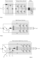
- FC systems require a two-stage power conditioning stage, where a DC-DC converter is utilized before the DC-AC converter in order to achieve the right voltage levels for either LV or MV AC grid integration as shown in Figure 1 .
- a DC-DC converter is utilized before the DC-AC converter in order to achieve the right voltage levels for either LV or MV AC grid integration as shown in Figure 1 .
- an isolating or step-up transformer can be utilized.
- SSI split-source inverter
- Figure 2 Another approach is to utilize a single-stage solution, such as the split-source inverter (SSI) shown in Figure 2 , in which the boosting capability is integrated within the inversion operation.
- This integrated solution uses the inverter switches with the addition diodes connected to a common inductor to achieve the boosting properties, i.e. it avoids the utilization of extra active switches and gate drive circuits.
- the operation of the SSI is described in A. Abdelhakim, P. Mattavelli and G. Spiazzi, "Three-Phase Split-Source Inverter (SSI): Analysis and Modulation," in IEEE Transactions on Power Electronics, vol. 31, no. 11, pp. 7451-7461, Nov. 2016 .
- This inverter uses at least one of the lower semiconductor switches to charge the input inductor, while using only one state to discharge this inductor over the inverter dc-link when all the upper switches are ON.
- the operation of the three-phase SSI does not require any special pulses to be generated or modifications of the standard modulation schemes of the voltage source inverter (VSI) for its basic operation. Hence, the same modulation schemes of the VSI can be applied to the SSI.
- An object of the present invention is to provide a buck-assisted split-source converter so as to alleviate the above disadvantage relating to utilization of the voltage.
- the object of the invention is achieved by an inverter circuit which characterized by what is stated in the independent claim.
- the preferred embodiments of the invention are disclosed in the dependent claims.
- the invention is based on the idea of modifying the configuration of the SSI circuit with minimum amount of additional components and without affecting the modulation of the inverter circuit.
- the circuit of the invention With the circuit of the invention voltage stresses of the inverter switch components are reduced and at the same time DC-link utilization is increased when compared to known SSI configuration. These advantages together with standard modulation of the inverter lead to a structure which is more efficient in use. Especially in connection with low voltage sources, such as fuel cells, the circuit of the invention provides efficient DC to AC conversion.
- Figure 1 shows a configuration for feeding electrical energy to a grid from a fuel cell.
- a DC voltage V dc from a voltage source such as a fuel cell
- a boost converter In the second stage the boosted voltage is inverted with a voltage source inverter to a three phase AC voltage.
- a filter When feeding the voltage to the grid, a filter is also applied to smooth the voltage generated by the inverter.
- Figure 2 shows a known split-source inverter with a fuel cell 21.
- a split source inverter has a voltage source inverter bridge which is connected between the voltage of a DC link.
- DC link of Figure 2 has a capacitor 22 to sustain the voltage of the DC link. The voltage of the DC link is used to produce alternating voltage using the switches of the inverter bridge.
- a voltage from a voltage source 21 is boosted using the switch components of the inverter and an additional inductor 23. Further, additional diodes 24 are needed such that the DC link is not shorted.
- a fuel cell is provided as a voltage source 21 having voltage V FC .
- the inverter bridge formed of three parallel inverter legs, are modulated such that either upper or lower semiconductor switch of a phase is active. That is, the output voltages v a , v b , v c are formed of voltages of DC link using the upper or lower semiconductor switches.
- the upper switches are connected to positive rail 25 of the DC link and the lower switches are connected to negative rail 26 of the DC link.
- the inductor When during the modulation of the switches of the inverter a state in which all the upper switches are conductive is selected, the inductor is discharged and pushes current through the switch components to the capacitor 22, and thereby charges the capacitor. Such a state is typically reached during normal modulation scheme, and additional measures to charge the capacitor are not required.
- the voltage of the voltage source 21 is effectively boosted with the switch components of the inverter bridge during modulation of the switch components.
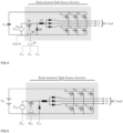
- FIG. 3 shows a main circuit of the present invention.
- the buck-assisted split-source inverter comprising a DC link having two voltage rails 31, 32 and at least two pairs of series connected switches with antiparallel connected diodes between the rails of the DC link, the center points of the series connected switches forming the phase outputs of the inverter
- FIG. 3 a three-phase inverter bridge is shown having upper switch components S a,u , S b,u , S c,u and lower switch components S a,l , S b,l , S c,l .
- each switch component of the inverter bridge has also a parallel connected diode to enable flow of current to both directions.
- the center points of the switches form phase outputs of the inverter.
- the output voltages being denoted as v a , v b , and v c .
- the buck-assisted split-source inverter comprises a first connection point 33 and a second connection point 34 for receiving voltage terminals of a fuel cell, one of the two voltage rails forming the first connection point 33.
- the buck-assisted split-source inverter is shown with a fuel cell 35 connected to the circuit.
- the connection points 33, 34 are provided in the circuit for receiving the fuel cells and are thus terminals for connecting voltage outputs of a fuel cell.
- the first connecting point is shown to be the DC voltage rail 32, which is the negative voltage rail of the DC link. In another embodiment discussed below, the first connecting point is the positive voltage rail 31.
- the buck-assisted split-source inverter comprises further a switch component 36 and an inductor 37 connected in series.
- the series connection has a first end formed of a terminal of the switch component 36 and a second end formed of a terminal of the inductor 37 The first end of the series connection forms the second connection point 34 for receiving a voltage terminal of a fuel cell.
- the inverter of the invention comprises at least two first diodes 39 having one of their corresponding terminals connected together and to the second end of the series connection of the switch component and the inductor.
- the other terminals of the at least two first diodes 39 being connected to separate phase outputs of the inverter.
- Figure 3 shows an embodiment with three phases and therefore also three first diodes 39.
- the diodes are connected such that their anodes are connected to the inductor, allowing current to pass from the inductor towards the inverter bridge.
- Figure 3 further shows a second diode 40 having first and second terminals, the first terminal being connected to the point between the switch component 36 and the inductor 37.
- the second terminal of the second diode 40 connected to the voltage rail 32 forming the first connection point 33, the polarity of the second diode corresponding to the polarities of the at least two first diodes such that a current path is formed through the second diode and the at least two first diodes.
- the polarity of the diode blocks the voltage of the point between the switch component 36.
- the switch component 36 of the invention is adapted to be controlled conductive when any one of the switches connected to voltage rail forming the first connection point 33 is controlled conductive.
- the switch component 36 when any one of the lower switches S a,l , S b,l , S a,l is controlled conductive, the switch component 36 is also controlled conductive. In Figure 3 , this is shown as an OR circuit 41 which receives control signals of the lower switches and outputs the logical OR of the inputted signals as a control signal for the switch component 36.
- the circuit of the invention differs from the known structure in that it comprises the switch component 36 and the second diode 40.
- the operation of the circuit of the invention corresponds to the known structure except that the switch component 36 is controlled conductive when any of the switches connected to the first connection point is controlled conductive.
- a three phase inverter can produce eight different switching states which may also be called output voltage vectors. From these states two are zero states in which either all of the upper switches or all of the lower switches are conductive, and the voltage between the output phases of the inverter is zero.
- the switch component 36 is also not conducting, and the current flows through the second diode 40.
- the voltage conversion gain can be further modified due to the extra degree of freedom in modulating the switch component 36. This can result in reduced voltage stresses across the DC-link in order to obtain the same AC voltage.
- Figure 4 shows another embodiment of the invention.
- the control of the switch 36 is affected by an additional control signal Signal.
- An AND gate 45 is shown to provide control to the switch 36, and the inputs to the AND gate are the additional control signal and the output of an OR gate 41.
- the OR gate receives control information from the lower switches similarly as in connection with the embodiment of Figure 3 .
- the switch component 36 is controlled conductive if anyone of the lower switch components are controlled conductive and if the additional control signal is in a logical high state.
- the switch component 36 can be set in a blocking state although one of the lower switches is controlled conductive.
- the control signal is kept active, the control information from the lower semiconductor switches is passed to the swich component.
- the switch 36 can be controlled to a blocking state.
- the current path through the lower switch components charge the inductor 37 from the voltage of the fuel cell 35. If the current path from the fuel cell is opened with the switch component when current is flowing trough the lower semiconductor switches, the current path is changed to the diode 40, and the current is being pushed from the inductor 37. As the inductor is discharged through the diode 40, the energy for the next charging cycle of the DC link is reduced.
- the additional signal Signal enables therefore to lower the DC link voltage.
- the lowering of the DC link voltage may lead to higher utilization of the DC link voltage as a higher modulation index can be employed in the control of the inverter bridge.
- the voltage of the DC voltage link is supported by capacitor 42 which is charged during the operation from the fuel cell.
- Figure 5 shows another embodiment, in which a battery or a battery unit is connected to the DC link. During operation, the battery is charged and discharged.
- FIG. 6 shows another embodiment of the invention.
- a separate boost converter is connected to the DC link.
- Voltage to the boost converter is obtained from a battery or a battery unit.
- the boost converter is operated in a known manner to control the voltage of the DC link.
- the boost converter is operated such that a fixed DC voltage is obtained in the DC link.
- the DC link voltage is sustained using a supercapacitor.
- the battery or battery unit of Figure 6 is replaced with a supercapacitor.
- FIG. 7 shows another embodiment of the invention, in which a boost converter is used to control the DC link voltage as in Figure 6 .
- a battery or battery unit with voltage V B is connected to the output of the boost converter and thereby also to the input of the split-source inverter.
- a super capacitor with voltage Vsc is connected to feed power to the boost converter.
- fuel cell, batteries and supercapacitors can be integrated with minimal converter requirements.
- the input terminals for the fuel cell are provided such that one of the input terminal is the negative DC link.
- the first connection point is formed of a negative voltage rail of the DC link, the anodes of the at least two first diodes are connected together and the anode of the second diode being connected to the negative voltage rail of the DC link.
- the first connection point is formed of a positive voltage rail of the DC link, the cathodes of the at least two first diodes being connected together and the cathode of the second diode being connected to the positive voltage rail of the DC link.
- the fuel cell is adapted to be connected to the positive voltage rail from it's positive output.
- the state of the output voltage in which the energy storage of the DC link is charged is when all of the lower semiconductor switches of the inverter bridge are controlled conductive. Further, the inductor is charged and the switch component is controlled conductive when any of the upper switches of the inverter bridge is controlled conductive.
- the embodiments of the invention presented in Figures 6 and 7 enable to integrate different energy sources to a converter structure.
- the additional boost converter in the input of the buck-assisted split-source converter may be controlled with different control schemes.
- the high-level control of the split-source converter and the additional boost converter may be synchronized to take into account the different energy sources used in the structure.
Landscapes
- Engineering & Computer Science (AREA)
- Power Engineering (AREA)
- Dc-Dc Converters (AREA)
- Inverter Devices (AREA)
Abstract
Description
- The present invention relates to an inverter, and particularly to a split-source inverter having a fuel cell as a source of energy.
- The integration of low-voltage (LV) energy sources, such as photovoltaic (PV) and fuel cell (FC), to the ac grids has been a relevant topic for research over the past few years. On top of that, integrating these energy sources with medium-voltage (MV) grids is gaining higher attention, due to the seen merits behind the MV integration at higher power levels. PV applications usually stack solar panels to achieve voltages up to 1.5 kV, however, the same is not true for FC that still have limitations in output voltage, where the highest voltage range seen in the market is 400~700V. Therefore, the integration of FC to LV or MV grid requires the use of a step-up dc-dc converter and an inverter to connect it to the AC grid, where a high step-up converter or transformer is a must with the MV grid.
- In general, FC systems require a two-stage power conditioning stage, where a DC-DC converter is utilized before the DC-AC converter in order to achieve the right voltage levels for either LV or MV AC grid integration as shown in
Figure 1 . On top of that, an isolating or step-up transformer can be utilized. - Another approach is to utilize a single-stage solution, such as the split-source inverter (SSI) shown in
Figure 2 , in which the boosting capability is integrated within the inversion operation. This integrated solution uses the inverter switches with the addition diodes connected to a common inductor to achieve the boosting properties, i.e. it avoids the utilization of extra active switches and gate drive circuits. The operation of the SSI is described in A. Abdelhakim, P. Mattavelli and G. Spiazzi, "Three-Phase Split-Source Inverter (SSI): Analysis and Modulation," in IEEE Transactions on Power Electronics, vol. 31, no. 11, pp. 7451-7461, Nov. 2016. This inverter uses at least one of the lower semiconductor switches to charge the input inductor, while using only one state to discharge this inductor over the inverter dc-link when all the upper switches are ON. The operation of the three-phase SSI does not require any special pulses to be generated or modifications of the standard modulation schemes of the voltage source inverter (VSI) for its basic operation. Hence, the same modulation schemes of the VSI can be applied to the SSI. - When SSI topology is employed with voltage sources, such as fuel cells, it is important that the utilization of the available voltage is as high as possible.
- An object of the present invention is to provide a buck-assisted split-source converter so as to alleviate the above disadvantage relating to utilization of the voltage. The object of the invention is achieved by an inverter circuit which characterized by what is stated in the independent claim. The preferred embodiments of the invention are disclosed in the dependent claims.
- The invention is based on the idea of modifying the configuration of the SSI circuit with minimum amount of additional components and without affecting the modulation of the inverter circuit.
- With the circuit of the invention voltage stresses of the inverter switch components are reduced and at the same time DC-link utilization is increased when compared to known SSI configuration. These advantages together with standard modulation of the inverter lead to a structure which is more efficient in use. Especially in connection with low voltage sources, such as fuel cells, the circuit of the invention provides efficient DC to AC conversion.
- In the following the invention will be described in greater detail by means of preferred embodiments with reference to the attached drawings, in which
-
Figure 1 shows a conventional fuel cell integration with AC loads; -
Figure 2 shows a known split-source inverter structure for fuel cell integration with AC loads; and -
Figures 3 ,4 ,5 ,6 and 7 show embodiments of a buck-assisted split-source inverter of the invention. -
Figure 1 shows a configuration for feeding electrical energy to a grid from a fuel cell. In the configuration a DC voltage Vdc from a voltage source, such as a fuel cell, is first boosted with a boost converter. In the second stage the boosted voltage is inverted with a voltage source inverter to a three phase AC voltage. When feeding the voltage to the grid, a filter is also applied to smooth the voltage generated by the inverter. -
Figure 2 shows a known split-source inverter with afuel cell 21. A split source inverter has a voltage source inverter bridge which is connected between the voltage of a DC link. DC link ofFigure 2 has acapacitor 22 to sustain the voltage of the DC link. The voltage of the DC link is used to produce alternating voltage using the switches of the inverter bridge. - In a split-source inverter as shown in
Figure 2 , a voltage from avoltage source 21 is boosted using the switch components of the inverter and anadditional inductor 23. Further,additional diodes 24 are needed such that the DC link is not shorted. Although the operation of the split-source inverter ofFigure 2 is known as such, the following description of operation is provided. - In the example of
Figure 2 , a fuel cell is provided as avoltage source 21 having voltage VFC. The inverter bridge, formed of three parallel inverter legs, are modulated such that either upper or lower semiconductor switch of a phase is active. That is, the output voltages va, vb, vc are formed of voltages of DC link using the upper or lower semiconductor switches. The upper switches are connected topositive rail 25 of the DC link and the lower switches are connected tonegative rail 26 of the DC link. - When the switches of the inverter bridge are modulated, current from the
fuel cell 21 is flowing. When any of the lower switch components are conducting, theinductor 23 is charged from thevoltage source 21. That is, a current path is formed from the voltage source through theinductor 23, the conducting switch and corresponding diode to thenegative rail 26 of the DC link and back tosource 21. When one or more of the lower switch components are conductive, the voltage of the capacitor is lowered as current to the load is provided through the active upper switches. - When during the modulation of the switches of the inverter a state in which all the upper switches are conductive is selected, the inductor is discharged and pushes current through the switch components to the
capacitor 22, and thereby charges the capacitor. Such a state is typically reached during normal modulation scheme, and additional measures to charge the capacitor are not required. - In a split-source inverter the voltage of the
voltage source 21 is effectively boosted with the switch components of the inverter bridge during modulation of the switch components. -
Figure 3 shows a main circuit of the present invention. The buck-assisted split-source inverter comprising a DC link having twovoltage rails - In
Figure 3 a three-phase inverter bridge is shown having upper switch components Sa,u, Sb,u, Sc,u and lower switch components Sa,l, Sb,l, Sc,l. It is to be noted, that each switch component of the inverter bridge has also a parallel connected diode to enable flow of current to both directions. The center points of the switches form phase outputs of the inverter. The output voltages being denoted as va, vb, and vc. - Further, according to the invention, the buck-assisted split-source inverter comprises a
first connection point 33 and asecond connection point 34 for receiving voltage terminals of a fuel cell, one of the two voltage rails forming thefirst connection point 33. InFigure 3 , the buck-assisted split-source inverter is shown with afuel cell 35 connected to the circuit. Theconnection points - In the embodiment of
Figure 3 , the first connecting point is shown to be theDC voltage rail 32, which is the negative voltage rail of the DC link. In another embodiment discussed below, the first connecting point is thepositive voltage rail 31. - As shown in
Figure 3 , the buck-assisted split-source inverter comprises further aswitch component 36 and aninductor 37 connected in series. The series connection has a first end formed of a terminal of theswitch component 36 and a second end formed of a terminal of theinductor 37 The first end of the series connection forms thesecond connection point 34 for receiving a voltage terminal of a fuel cell. - Further, the inverter of the invention comprises at least two
first diodes 39 having one of their corresponding terminals connected together and to the second end of the series connection of the switch component and the inductor. The other terminals of the at least twofirst diodes 39 being connected to separate phase outputs of the inverter.Figure 3 shows an embodiment with three phases and therefore also threefirst diodes 39. The diodes are connected such that their anodes are connected to the inductor, allowing current to pass from the inductor towards the inverter bridge. -
Figure 3 further shows asecond diode 40 having first and second terminals, the first terminal being connected to the point between theswitch component 36 and theinductor 37. The second terminal of thesecond diode 40 connected to thevoltage rail 32 forming thefirst connection point 33, the polarity of the second diode corresponding to the polarities of the at least two first diodes such that a current path is formed through the second diode and the at least two first diodes. The polarity of the diode blocks the voltage of the point between theswitch component 36. Theswitch component 36 of the invention is adapted to be controlled conductive when any one of the switches connected to voltage rail forming thefirst connection point 33 is controlled conductive. In the embodiment ofFigure 3 , when any one of the lower switches Sa,l, Sb,l, Sa,l is controlled conductive, theswitch component 36 is also controlled conductive. InFigure 3 , this is shown as an ORcircuit 41 which receives control signals of the lower switches and outputs the logical OR of the inputted signals as a control signal for theswitch component 36. - When comparing
Figures 2 and 3 , it can be seen that the circuit of the invention differs from the known structure in that it comprises theswitch component 36 and thesecond diode 40. The operation of the circuit of the invention corresponds to the known structure except that theswitch component 36 is controlled conductive when any of the switches connected to the first connection point is controlled conductive. Generally, a three phase inverter can produce eight different switching states which may also be called output voltage vectors. From these states two are zero states in which either all of the upper switches or all of the lower switches are conductive, and the voltage between the output phases of the inverter is zero. In connection with the embodiment ofFigure 3 , when all the upper switches are controlled conductive, the current from theinductor 37 is pushed through the upper switch components to charge the DC link. According to the embodiment, as none of the semiconductor switches connected to the first connection point are conducting, theswitch component 36 is also not conducting, and the current flows through thesecond diode 40. - Due to the utilization of the
switch component 36 with the inverter bridge, the voltage conversion gain can be further modified due to the extra degree of freedom in modulating theswitch component 36. This can result in reduced voltage stresses across the DC-link in order to obtain the same AC voltage. -
Figure 4 shows another embodiment of the invention. In the embodiment the control of theswitch 36 is affected by an additional control signal Signal. An ANDgate 45 is shown to provide control to theswitch 36, and the inputs to the AND gate are the additional control signal and the output of anOR gate 41. The OR gate receives control information from the lower switches similarly as in connection with the embodiment ofFigure 3 . In other words, in the embodiment ofFigure 4 , theswitch component 36 is controlled conductive if anyone of the lower switch components are controlled conductive and if the additional control signal is in a logical high state. - With the control signal Signal, the
switch component 36 can be set in a blocking state although one of the lower switches is controlled conductive. When the control signal is kept active, the control information from the lower semiconductor switches is passed to the swich component. With the control signal theswitch 36 can be controlled to a blocking state. As described above, the current path through the lower switch components charge theinductor 37 from the voltage of thefuel cell 35. If the current path from the fuel cell is opened with the switch component when current is flowing trough the lower semiconductor switches, the current path is changed to thediode 40, and the current is being pushed from theinductor 37. As the inductor is discharged through thediode 40, the energy for the next charging cycle of the DC link is reduced. The additional signal Signal enables therefore to lower the DC link voltage. The lowering of the DC link voltage may lead to higher utilization of the DC link voltage as a higher modulation index can be employed in the control of the inverter bridge. - In the embodiments of
Figure 3 andFigure 4 , the voltage of the DC voltage link is supported by capacitor 42 which is charged during the operation from the fuel cell. -
Figure 5 shows another embodiment, in which a battery or a battery unit is connected to the DC link. During operation, the battery is charged and discharged. -
Figure 6 shows another embodiment of the invention. In this embodiment, a separate boost converter is connected to the DC link. Voltage to the boost converter is obtained from a battery or a battery unit. The boost converter is operated in a known manner to control the voltage of the DC link. Preferably, the boost converter is operated such that a fixed DC voltage is obtained in the DC link. Instead of the battery or battery unit, in one embodiment, the DC link voltage is sustained using a supercapacitor. In such embodiment, the battery or battery unit ofFigure 6 is replaced with a supercapacitor. -
Figure 7 shows another embodiment of the invention, in which a boost converter is used to control the DC link voltage as inFigure 6 . InFigure 7 a battery or battery unit with voltage VB is connected to the output of the boost converter and thereby also to the input of the split-source inverter. A super capacitor with voltage Vsc is connected to feed power to the boost converter. In the structure ofFigure 7 , fuel cell, batteries and supercapacitors can be integrated with minimal converter requirements. - In the embodiments shown in the
Figures 3 to 7 , the input terminals for the fuel cell are provided such that one of the input terminal is the negative DC link. In such embodiments the first connection point is formed of a negative voltage rail of the DC link, the anodes of the at least two first diodes are connected together and the anode of the second diode being connected to the negative voltage rail of the DC link. - In another embodiment the first connection point is formed of a positive voltage rail of the DC link, the cathodes of the at least two first diodes being connected together and the cathode of the second diode being connected to the positive voltage rail of the DC link. In such an embodiment the fuel cell is adapted to be connected to the positive voltage rail from it's positive output. In such a case, the state of the output voltage in which the energy storage of the DC link is charged is when all of the lower semiconductor switches of the inverter bridge are controlled conductive. Further, the inductor is charged and the switch component is controlled conductive when any of the upper switches of the inverter bridge is controlled conductive.
- The embodiments of the invention presented in
Figures 6 and 7 enable to integrate different energy sources to a converter structure. The additional boost converter in the input of the buck-assisted split-source converter may be controlled with different control schemes. The high-level control of the split-source converter and the additional boost converter may be synchronized to take into account the different energy sources used in the structure. - It will be obvious to a person skilled in the art that, as the technology advances, the inventive concept can be implemented in various ways. The invention and its embodiments are not limited to the examples described above but may vary within the scope of the claims.
Claims (8)
- A buck-assisted split-source inverter comprisinga DC link having two voltage rails,at least two pairs of series connected switches with antiparallel diodes connected between the rails of the DC link, the center points of the series connected switches forming the phase outputs of the inverter,a first connection point and a second connection point for receiving voltage terminals of a fuel cell, one of the two voltage rails forming the first connection point,a switch component and an inductor connected in series having a first end formed of a terminal of the switch component and a second end formed of a terminal of the inductor, the first end forming the second connection point for receiving a voltage terminal of a fuel cell,at least two first diodes having one of their corresponding terminals connected together and to the second end of the series connection of the switch component and the inductor, and the other terminals of the at least two first diodes being connected to separate phase outputs of the inverter,a second diode having first and second terminals, the first terminal being connected to the point between the switch component and the inductor and the second terminal being connected to the voltage rail forming the first connection point, the polarity of the second diode corresponding to the polarities of the at least two first diodes such that a current path is formed through the second diode and the at least two first diodes,wherein the switch component is adapted to be controlled conductive when any one of the lower switches connected to voltage rail forming the first connection point is controlled conductive.
- A buck-assisted split-source inverter according to claim 1, wherein the first connection point is formed of a negative voltage rail of the DC link, the anodes of the at least two first diodes being connected together and the anode of the second diode being connected to the negative voltage rail of the DC link.
- A buck-assisted split-source inverter according to claim 1, wherein the first connection point is formed of a positive voltage rail of the DC link, the cathodes of the at least two first diodes being connected together and the cathode of the second diode being connected to the positive voltage rail of the DC link.
- A buck-assisted split-source inverter according to claim 1, 2 or 3, wherein the switch component is adapted to be controlled conductive when any one of the switches connected to voltage rail forming the first connection point is controlled conductive and when a control signal is active.
- A buck-assisted split-source inverter according to any one of the claims 1 to 4, wherein the DC link of the buck-assisted split-source inverter comprises a capacitor connected between the rails of the DC link.
- A buck-assisted split-source inverter according to any one of the claims 1 to 4, wherein the DC link of the buck-assisted split-source inverter comprises a battery connected between the rails of the DC link.
- A buck-assisted split-source inverter according to any one of the claims 1 to 6, wherein the buck-assisted split-source inverter comprises a boost converter connected to the DC link, the boost converter receiving power from a battery or a super capacitor.
- A buck-assisted split-source inverter according claim 7, wherein the DC link comprises a battery connected between the rails of the DC link, wherein the battery is connected to the output of the boost converter.
Priority Applications (3)
| Application Number | Priority Date | Filing Date | Title |
|---|---|---|---|
| EP21204184.2A EP4170879B1 (en) | 2021-10-22 | 2021-10-22 | Buck-assisted split-source inverter |
| CN202211295698.5A CN116015087A (en) | 2021-10-22 | 2022-10-21 | Buck Auxiliary Split Source Inverter |
| US18/048,804 US11962244B2 (en) | 2021-10-22 | 2022-10-21 | Buck-assisted split-source inverter |
Applications Claiming Priority (1)
| Application Number | Priority Date | Filing Date | Title |
|---|---|---|---|
| EP21204184.2A EP4170879B1 (en) | 2021-10-22 | 2021-10-22 | Buck-assisted split-source inverter |
Publications (3)
| Publication Number | Publication Date |
|---|---|
| EP4170879A1 true EP4170879A1 (en) | 2023-04-26 |
| EP4170879C0 EP4170879C0 (en) | 2024-07-17 |
| EP4170879B1 EP4170879B1 (en) | 2024-07-17 |
Family
ID=78371953
Family Applications (1)
| Application Number | Title | Priority Date | Filing Date |
|---|---|---|---|
| EP21204184.2A Active EP4170879B1 (en) | 2021-10-22 | 2021-10-22 | Buck-assisted split-source inverter |
Country Status (3)
| Country | Link |
|---|---|
| US (1) | US11962244B2 (en) |
| EP (1) | EP4170879B1 (en) |
| CN (1) | CN116015087A (en) |
Cited By (2)
| Publication number | Priority date | Publication date | Assignee | Title |
|---|---|---|---|---|
| CN116633185A (en) * | 2023-07-19 | 2023-08-22 | 南京理工大学 | Boost grid-connected inverter and control method thereof |
| CN117691887A (en) * | 2024-01-31 | 2024-03-12 | 湖南大学 | A supercapacitor energy storage type high overload single-phase inverter circuit and its control method |
Families Citing this family (1)
| Publication number | Priority date | Publication date | Assignee | Title |
|---|---|---|---|---|
| CN117811402B (en) * | 2023-12-27 | 2025-02-14 | 南京理工大学 | A boost type three-port energy storage inverter and control method thereof |
Citations (2)
| Publication number | Priority date | Publication date | Assignee | Title |
|---|---|---|---|---|
| DE102017201155A1 (en) * | 2017-01-25 | 2018-07-26 | Robert Bosch Gmbh | Arrangement for transmitting electrical energy, drive train and working device |
| WO2021104621A1 (en) * | 2019-11-27 | 2021-06-03 | Abb Schweiz Ag | Onboard powertrain for agv |
Family Cites Families (3)
| Publication number | Priority date | Publication date | Assignee | Title |
|---|---|---|---|---|
| KR101653837B1 (en) * | 2009-12-24 | 2016-09-02 | 두산인프라코어 주식회사 | Power transformer for hybrid industrial vehicle |
| US10381951B1 (en) * | 2018-11-30 | 2019-08-13 | The Florida International University Board Of Trustees | Family of modular quasi-resonant inverters |
| CN113517824B (en) * | 2021-06-24 | 2022-07-22 | 南京航空航天大学 | Single-phase single-stage six-switch double-output split-source boosting inverter |
-
2021
- 2021-10-22 EP EP21204184.2A patent/EP4170879B1/en active Active
-
2022
- 2022-10-21 CN CN202211295698.5A patent/CN116015087A/en active Pending
- 2022-10-21 US US18/048,804 patent/US11962244B2/en active Active
Patent Citations (2)
| Publication number | Priority date | Publication date | Assignee | Title |
|---|---|---|---|---|
| DE102017201155A1 (en) * | 2017-01-25 | 2018-07-26 | Robert Bosch Gmbh | Arrangement for transmitting electrical energy, drive train and working device |
| WO2021104621A1 (en) * | 2019-11-27 | 2021-06-03 | Abb Schweiz Ag | Onboard powertrain for agv |
Non-Patent Citations (3)
| Title |
|---|
| ABDELHAKIM AHMED ET AL: "Three-Phase Split-Source Inverter (SSI): Analysis and Modulation", IEEE TRANSACTIONS ON POWER ELECTRONICS, INSTITUTE OF ELECTRICAL AND ELECTRONICS ENGINEERS, USA, vol. 31, no. 11, 1 November 2016 (2016-11-01), pages 7451 - 7461, XP011615245, ISSN: 0885-8993, [retrieved on 20160624], DOI: 10.1109/TPEL.2015.2513204 * |
| G. SPIAZZI: "Three-Phase Split-Source Inverter (SSI): Analysis and Modulation", IEEE TRANSACTIONS ON POWER ELECTRONICS, vol. 31, no. 11, November 2016 (2016-11-01), pages 7451 - 7461, XP011615245, DOI: 10.1109/TPEL.2015.2513204 |
| ZHU JIANXIN ET AL: "A Dual-DC Output Three-Phase Three-Level AC-DC Converter for Low-Frequency Pulsed Power Decoupling Applications", IEEE TRANSACTIONS ON INDUSTRIAL ELECTRONICS, IEEE SERVICE CENTER, PISCATAWAY, NJ, USA, vol. 69, no. 1, 14 January 2021 (2021-01-14), pages 52 - 63, XP011881876, ISSN: 0278-0046, [retrieved on 20211001], DOI: 10.1109/TIE.2021.3050347 * |
Cited By (4)
| Publication number | Priority date | Publication date | Assignee | Title |
|---|---|---|---|---|
| CN116633185A (en) * | 2023-07-19 | 2023-08-22 | 南京理工大学 | Boost grid-connected inverter and control method thereof |
| CN116633185B (en) * | 2023-07-19 | 2023-11-10 | 南京理工大学 | Boost grid-connected inverter and control method thereof |
| CN117691887A (en) * | 2024-01-31 | 2024-03-12 | 湖南大学 | A supercapacitor energy storage type high overload single-phase inverter circuit and its control method |
| CN117691887B (en) * | 2024-01-31 | 2024-04-19 | 湖南大学 | Super-capacitor energy-storage type high-overload single-phase inverter circuit and control method thereof |
Also Published As
| Publication number | Publication date |
|---|---|
| EP4170879C0 (en) | 2024-07-17 |
| CN116015087A (en) | 2023-04-25 |
| EP4170879B1 (en) | 2024-07-17 |
| US11962244B2 (en) | 2024-04-16 |
| US20230125181A1 (en) | 2023-04-27 |
Similar Documents
| Publication | Publication Date | Title |
|---|---|---|
| US11962244B2 (en) | Buck-assisted split-source inverter | |
| Zhao et al. | A hybrid nine-level inverter with reduced components and simplified control | |
| JP2007166783A (en) | Power converter | |
| US20130038130A1 (en) | Dc-to-ac converter system and dc-to-ac converter circuit | |
| JP5132797B2 (en) | Power converter | |
| US20250373067A1 (en) | Multiple input converter and an uninterruptible power supply including the same | |
| CN100426644C (en) | Power converter | |
| Bughneda et al. | A single-phase multilevel inverter with reduced switch count for solar PV application | |
| Wageh et al. | A high gain split-source inverter with reduced input current ripple | |
| Dhasharatha et al. | A capacitor-based boost nine-level inverter with less switching device count | |
| Gaafar et al. | Multi‐input transformer‐less four‐wire microinverter with distributed MPPT for PV systems | |
| Al-Hitmi et al. | A switched-capacitor based multilevel inverter with extendable levels having enhanced voltage gain for renewable energy applications | |
| Cheng et al. | Hot-swappable grid-connected multilevel converter for battery energy storage system | |
| Koduri et al. | A nine level quadruple boost inverter with reduced switch count for stand alone PV applications | |
| Asapu et al. | Dual switch High Gain Boost Converter for DC microgrid Applications | |
| Salary et al. | Multi-stage DC-AC converter based on new DC-DC converter for energy conversion | |
| Roy et al. | A novel step-up multilevel inverter based on switched-capacitor technique for renewable energy conversion system | |
| Sandeep et al. | Switched-capacitor-based three-phase five-level inverter topology with reduced components | |
| Eswar et al. | THD Analysis of Hybrid Switched-Capacitor Integrated Multilevel Inverter Using Level-Shifted Modulation Techniques | |
| Shaw et al. | Switched-inductor based high voltage gain step-up DC-DC converter for photovoltaic micro-inverter application | |
| Neti et al. | Common ground single-phase single-stage transformerless inverter five levels using reduced components and switched capacitor cell | |
| Patel et al. | A Novel Switched Capacitors Based Multilevel Boost Inverter With Single DC Source For Three Phase Applications | |
| US12407274B2 (en) | Inverter topology circuit | |
| US20240195178A1 (en) | Power conversion device and control method thereof | |
| CN119401822B (en) | Double-separation-source multi-level converter and power supply system |
Legal Events
| Date | Code | Title | Description |
|---|---|---|---|
| PUAI | Public reference made under article 153(3) epc to a published international application that has entered the european phase |
Free format text: ORIGINAL CODE: 0009012 |
|
| STAA | Information on the status of an ep patent application or granted ep patent |
Free format text: STATUS: THE APPLICATION HAS BEEN PUBLISHED |
|
| AK | Designated contracting states |
Kind code of ref document: A1 Designated state(s): AL AT BE BG CH CY CZ DE DK EE ES FI FR GB GR HR HU IE IS IT LI LT LU LV MC MK MT NL NO PL PT RO RS SE SI SK SM TR |
|
| STAA | Information on the status of an ep patent application or granted ep patent |
Free format text: STATUS: REQUEST FOR EXAMINATION WAS MADE |
|
| 17P | Request for examination filed |
Effective date: 20230914 |
|
| RBV | Designated contracting states (corrected) |
Designated state(s): AL AT BE BG CH CY CZ DE DK EE ES FI FR GB GR HR HU IE IS IT LI LT LU LV MC MK MT NL NO PL PT RO RS SE SI SK SM TR |
|
| GRAP | Despatch of communication of intention to grant a patent |
Free format text: ORIGINAL CODE: EPIDOSNIGR1 |
|
| STAA | Information on the status of an ep patent application or granted ep patent |
Free format text: STATUS: GRANT OF PATENT IS INTENDED |
|
| RIC1 | Information provided on ipc code assigned before grant |
Ipc: H02M 7/797 20060101ALN20240123BHEP Ipc: H02M 3/158 20060101ALI20240123BHEP Ipc: H02M 7/5387 20070101ALI20240123BHEP Ipc: H02M 1/00 20060101AFI20240123BHEP |
|
| INTG | Intention to grant announced |
Effective date: 20240213 |
|
| GRAS | Grant fee paid |
Free format text: ORIGINAL CODE: EPIDOSNIGR3 |
|
| GRAA | (expected) grant |
Free format text: ORIGINAL CODE: 0009210 |
|
| STAA | Information on the status of an ep patent application or granted ep patent |
Free format text: STATUS: THE PATENT HAS BEEN GRANTED |
|
| AK | Designated contracting states |
Kind code of ref document: B1 Designated state(s): AL AT BE BG CH CY CZ DE DK EE ES FI FR GB GR HR HU IE IS IT LI LT LU LV MC MK MT NL NO PL PT RO RS SE SI SK SM TR |
|
| REG | Reference to a national code |
Ref country code: CH Ref legal event code: EP |
|
| REG | Reference to a national code |
Ref country code: DE Ref legal event code: R096 Ref document number: 602021015747 Country of ref document: DE |
|
| REG | Reference to a national code |
Ref country code: IE Ref legal event code: FG4D |
|
| U01 | Request for unitary effect filed |
Effective date: 20240813 |
|
| U07 | Unitary effect registered |
Designated state(s): AT BE BG DE DK EE FI FR IT LT LU LV MT NL PT RO SE SI Effective date: 20240902 |
|
| U20 | Renewal fee for the european patent with unitary effect paid |
Year of fee payment: 4 Effective date: 20241025 |
|
| PG25 | Lapsed in a contracting state [announced via postgrant information from national office to epo] |
Ref country code: NO Free format text: LAPSE BECAUSE OF FAILURE TO SUBMIT A TRANSLATION OF THE DESCRIPTION OR TO PAY THE FEE WITHIN THE PRESCRIBED TIME-LIMIT Effective date: 20241017 |
|
| PG25 | Lapsed in a contracting state [announced via postgrant information from national office to epo] |
Ref country code: GR Free format text: LAPSE BECAUSE OF FAILURE TO SUBMIT A TRANSLATION OF THE DESCRIPTION OR TO PAY THE FEE WITHIN THE PRESCRIBED TIME-LIMIT Effective date: 20241018 Ref country code: PL Free format text: LAPSE BECAUSE OF FAILURE TO SUBMIT A TRANSLATION OF THE DESCRIPTION OR TO PAY THE FEE WITHIN THE PRESCRIBED TIME-LIMIT Effective date: 20240717 |
|
| PG25 | Lapsed in a contracting state [announced via postgrant information from national office to epo] |
Ref country code: IS Free format text: LAPSE BECAUSE OF FAILURE TO SUBMIT A TRANSLATION OF THE DESCRIPTION OR TO PAY THE FEE WITHIN THE PRESCRIBED TIME-LIMIT Effective date: 20241117 |
|
| PG25 | Lapsed in a contracting state [announced via postgrant information from national office to epo] |
Ref country code: HR Free format text: LAPSE BECAUSE OF FAILURE TO SUBMIT A TRANSLATION OF THE DESCRIPTION OR TO PAY THE FEE WITHIN THE PRESCRIBED TIME-LIMIT Effective date: 20240717 |
|
| PG25 | Lapsed in a contracting state [announced via postgrant information from national office to epo] |
Ref country code: ES Free format text: LAPSE BECAUSE OF FAILURE TO SUBMIT A TRANSLATION OF THE DESCRIPTION OR TO PAY THE FEE WITHIN THE PRESCRIBED TIME-LIMIT Effective date: 20240717 Ref country code: RS Free format text: LAPSE BECAUSE OF FAILURE TO SUBMIT A TRANSLATION OF THE DESCRIPTION OR TO PAY THE FEE WITHIN THE PRESCRIBED TIME-LIMIT Effective date: 20241017 |
|
| PG25 | Lapsed in a contracting state [announced via postgrant information from national office to epo] |
Ref country code: RS Free format text: LAPSE BECAUSE OF FAILURE TO SUBMIT A TRANSLATION OF THE DESCRIPTION OR TO PAY THE FEE WITHIN THE PRESCRIBED TIME-LIMIT Effective date: 20241017 Ref country code: PL Free format text: LAPSE BECAUSE OF FAILURE TO SUBMIT A TRANSLATION OF THE DESCRIPTION OR TO PAY THE FEE WITHIN THE PRESCRIBED TIME-LIMIT Effective date: 20240717 Ref country code: NO Free format text: LAPSE BECAUSE OF FAILURE TO SUBMIT A TRANSLATION OF THE DESCRIPTION OR TO PAY THE FEE WITHIN THE PRESCRIBED TIME-LIMIT Effective date: 20241017 Ref country code: IS Free format text: LAPSE BECAUSE OF FAILURE TO SUBMIT A TRANSLATION OF THE DESCRIPTION OR TO PAY THE FEE WITHIN THE PRESCRIBED TIME-LIMIT Effective date: 20241117 Ref country code: HR Free format text: LAPSE BECAUSE OF FAILURE TO SUBMIT A TRANSLATION OF THE DESCRIPTION OR TO PAY THE FEE WITHIN THE PRESCRIBED TIME-LIMIT Effective date: 20240717 Ref country code: GR Free format text: LAPSE BECAUSE OF FAILURE TO SUBMIT A TRANSLATION OF THE DESCRIPTION OR TO PAY THE FEE WITHIN THE PRESCRIBED TIME-LIMIT Effective date: 20241018 Ref country code: ES Free format text: LAPSE BECAUSE OF FAILURE TO SUBMIT A TRANSLATION OF THE DESCRIPTION OR TO PAY THE FEE WITHIN THE PRESCRIBED TIME-LIMIT Effective date: 20240717 |
|
| PG25 | Lapsed in a contracting state [announced via postgrant information from national office to epo] |
Ref country code: SM Free format text: LAPSE BECAUSE OF FAILURE TO SUBMIT A TRANSLATION OF THE DESCRIPTION OR TO PAY THE FEE WITHIN THE PRESCRIBED TIME-LIMIT Effective date: 20240717 |
|
| PG25 | Lapsed in a contracting state [announced via postgrant information from national office to epo] |
Ref country code: CZ Free format text: LAPSE BECAUSE OF FAILURE TO SUBMIT A TRANSLATION OF THE DESCRIPTION OR TO PAY THE FEE WITHIN THE PRESCRIBED TIME-LIMIT Effective date: 20240717 |
|
| PG25 | Lapsed in a contracting state [announced via postgrant information from national office to epo] |
Ref country code: SK Free format text: LAPSE BECAUSE OF FAILURE TO SUBMIT A TRANSLATION OF THE DESCRIPTION OR TO PAY THE FEE WITHIN THE PRESCRIBED TIME-LIMIT Effective date: 20240717 |
|
| PLBE | No opposition filed within time limit |
Free format text: ORIGINAL CODE: 0009261 |
|
| STAA | Information on the status of an ep patent application or granted ep patent |
Free format text: STATUS: NO OPPOSITION FILED WITHIN TIME LIMIT |
|
| REG | Reference to a national code |
Ref country code: CH Ref legal event code: PL |
|
| 26N | No opposition filed |
Effective date: 20250422 |
|
| PG25 | Lapsed in a contracting state [announced via postgrant information from national office to epo] |
Ref country code: MC Free format text: LAPSE BECAUSE OF FAILURE TO SUBMIT A TRANSLATION OF THE DESCRIPTION OR TO PAY THE FEE WITHIN THE PRESCRIBED TIME-LIMIT Effective date: 20240717 |
|
| PG25 | Lapsed in a contracting state [announced via postgrant information from national office to epo] |
Ref country code: CH Free format text: LAPSE BECAUSE OF NON-PAYMENT OF DUE FEES Effective date: 20241031 |
|
| PG25 | Lapsed in a contracting state [announced via postgrant information from national office to epo] |
Ref country code: IE Free format text: LAPSE BECAUSE OF NON-PAYMENT OF DUE FEES Effective date: 20241022 |
|
| U20 | Renewal fee for the european patent with unitary effect paid |
Year of fee payment: 5 Effective date: 20251028 |
|
| PG25 | Lapsed in a contracting state [announced via postgrant information from national office to epo] |
Ref country code: CY Free format text: LAPSE BECAUSE OF FAILURE TO SUBMIT A TRANSLATION OF THE DESCRIPTION OR TO PAY THE FEE WITHIN THE PRESCRIBED TIME-LIMIT; INVALID AB INITIO Effective date: 20211022 |
|
| PG25 | Lapsed in a contracting state [announced via postgrant information from national office to epo] |
Ref country code: HU Free format text: LAPSE BECAUSE OF FAILURE TO SUBMIT A TRANSLATION OF THE DESCRIPTION OR TO PAY THE FEE WITHIN THE PRESCRIBED TIME-LIMIT; INVALID AB INITIO Effective date: 20211022 |