EP4170866B1 - Elektronische vorrichtung zur drahtlosen stromübertragung und betriebsverfahren dafür - Google Patents
Elektronische vorrichtung zur drahtlosen stromübertragung und betriebsverfahren dafür Download PDFInfo
- Publication number
- EP4170866B1 EP4170866B1 EP21828358.8A EP21828358A EP4170866B1 EP 4170866 B1 EP4170866 B1 EP 4170866B1 EP 21828358 A EP21828358 A EP 21828358A EP 4170866 B1 EP4170866 B1 EP 4170866B1
- Authority
- EP
- European Patent Office
- Prior art keywords
- power transmission
- power
- electronic device
- magnetic element
- polarity
- Prior art date
- Legal status (The legal status is an assumption and is not a legal conclusion. Google has not performed a legal analysis and makes no representation as to the accuracy of the status listed.)
- Active
Links
Images


Classifications
-
- H—ELECTRICITY
- H02—GENERATION; CONVERSION OR DISTRIBUTION OF ELECTRIC POWER
- H02J—ELECTRIC POWER NETWORKS; CIRCUIT ARRANGEMENTS OR SYSTEMS FOR SUPPLYING OR DISTRIBUTING ELECTRIC POWER; SYSTEMS FOR STORING ELECTRIC ENERGY
- H02J50/00—Circuit arrangements or systems for wireless supply or distribution of electric power
- H02J50/10—Circuit arrangements or systems for wireless supply or distribution of electric power using inductive coupling
- H02J50/12—Circuit arrangements or systems for wireless supply or distribution of electric power using inductive coupling of the resonant type
-
- H—ELECTRICITY
- H02—GENERATION; CONVERSION OR DISTRIBUTION OF ELECTRIC POWER
- H02J—ELECTRIC POWER NETWORKS; CIRCUIT ARRANGEMENTS OR SYSTEMS FOR SUPPLYING OR DISTRIBUTING ELECTRIC POWER; SYSTEMS FOR STORING ELECTRIC ENERGY
- H02J50/00—Circuit arrangements or systems for wireless supply or distribution of electric power
- H02J50/40—Circuit arrangements or systems for wireless supply or distribution of electric power using two or more transmitting or receiving devices
-
- H—ELECTRICITY
- H02—GENERATION; CONVERSION OR DISTRIBUTION OF ELECTRIC POWER
- H02J—ELECTRIC POWER NETWORKS; CIRCUIT ARRANGEMENTS OR SYSTEMS FOR SUPPLYING OR DISTRIBUTING ELECTRIC POWER; SYSTEMS FOR STORING ELECTRIC ENERGY
- H02J50/00—Circuit arrangements or systems for wireless supply or distribution of electric power
- H02J50/50—Circuit arrangements or systems for wireless supply or distribution of electric power using additional energy repeaters between transmitting devices and receiving devices
- H02J50/502—Circuit arrangements or systems for wireless supply or distribution of electric power using additional energy repeaters between transmitting devices and receiving devices the energy repeater being integrated together with the emitter or the receiver
-
- H—ELECTRICITY
- H02—GENERATION; CONVERSION OR DISTRIBUTION OF ELECTRIC POWER
- H02J—ELECTRIC POWER NETWORKS; CIRCUIT ARRANGEMENTS OR SYSTEMS FOR SUPPLYING OR DISTRIBUTING ELECTRIC POWER; SYSTEMS FOR STORING ELECTRIC ENERGY
- H02J50/00—Circuit arrangements or systems for wireless supply or distribution of electric power
- H02J50/80—Circuit arrangements or systems for wireless supply or distribution of electric power involving the exchange of data, concerning supply or distribution of electric power, between transmitting devices and receiving devices
-
- H—ELECTRICITY
- H02—GENERATION; CONVERSION OR DISTRIBUTION OF ELECTRIC POWER
- H02J—ELECTRIC POWER NETWORKS; CIRCUIT ARRANGEMENTS OR SYSTEMS FOR SUPPLYING OR DISTRIBUTING ELECTRIC POWER; SYSTEMS FOR STORING ELECTRIC ENERGY
- H02J50/00—Circuit arrangements or systems for wireless supply or distribution of electric power
- H02J50/90—Circuit arrangements or systems for wireless supply or distribution of electric power involving detection or optimisation of position, e.g. alignment
Definitions
- Various embodiments relate to an electronic device and a method for wirelessly transmitting power.
- the wireless power transmission technology is a technology which converts electric energy into a form of electromagnetic waves having a frequency and wirelessly transfers the converted energy to a load (for example, an external electronic device) without a transmission line.
- the wireless power transmission technology may be a technology in which power is wirelessly transferred from a power transmission device to a power reception device without a connection between the power reception device and the power transmission device via a separate connector, so that a battery of the power reception device is charged.
- the wireless power transmission technology may include a magnetic induction scheme and a magnetic resonance scheme, and there may be various other types of wireless power transmission technologies.
- a magnetic induction type wireless power transmission system uses a scheme of transferring power by using a magnetic field induced in a coil, and is a technology which, using a magnetic field generated by a current flowing through a transmission coil, generates an electromotive force in a reception coil to cause an induced current to flow therethrough, so as to provide energy to a load (for example, an external electronic device).
- Representative standards of the magnetic induction scheme include wireless power consortium (WPC), power matters alliance (PMA), or the like, and a designated frequency band such as 110 to 205 kHz for WPC, and 227 to 357 kHz, and 118 to 153 kHz for PMA may be used as a frequency used for power transmission.
- Electronic devices capable of wireless power transmission may use different communication protocols and frequencies of signals for wireless power transmission according to manufacturers thereof.
- the power transmission device may require increased design difficulty and complexity in order to identify a power transmission scheme suitable for a power reception device.
- the time required to start charging may be increased because communication methods and configuration schemes of the multiple power transmission schemes are different.
- magnets having different polarities may be inserted in a power transmission device and a power reception device, respectively, and the power transmission device and the power reception device may be fixedly positioned using the magnets, in order to achieve efficient power transmission and minimize the phenomenon of induction heating.
- magnets having the same polarity are inserted in a power transmission device and a power reception device, mounting of the power reception device for wireless power transmission may be impossible.
- Various embodiments provide a power transmission device and an operating method thereof, wherein the power transmission device includes a rotatable magnet.
- the power reception device can identify the polarity of the magnet included in the power transmission device and determine a power transmission scheme suitable for the wireless power reception device among a plurality of power transmission schemes.
- An electronic device includes a sensor, a first magnetic element which can be rotated to have a polarity of one of a first pole and a second pole in a first direction, and a processor, wherein the processor is configured to, identify, through the sensor, a polarity of a one of first magnetic element and a second magnetic element and a strength of a magnetic force generated by approaching of the second magnetic element to the first magnetic element, the polarity being determined by the magnetic force, the second magnetic element being included in an external electronic device, determine a power transmission scheme among a plurality of power transmission schemes, based on the polarity and the strength of the magnetic force, and wirelessly transmit power to the external electronic device, based on the power transmission scheme.
- An operating method of an electronic device including a first magnetic element which can be rotated to have a polarity of one of a first pole and a second pole in a first direction includes identifying a polarity of one of a first magnetic element and a second magnetic element and a strength of a magnetic force generated by approaching of the second magnetic element to the first magnetic element, the polarity being determined by the magnetic force, the second magnetic element being included in an external electronic device, determining a power transmission scheme among a plurality of power transmission schemes, based on the polarity and the strength of the magnetic force, and wirelessly transmitting power to the external electronic device, based on the power transmission scheme.
- a computer-readable recording medium stores instructions configured to, when executed, cause a processor to: identify a polarity of one of a first magnetic element and a second magnetic element and a strength of a magnetic force generated by approaching of the second magnetic element to the first magnetic element, the polarity being determined by the magnetic force, the first magnetic element being included in an electronic device and being rotatable in a first direction to have a polarity of one of a first pole and a second pole, the second magnetic element being included in an external electronic device; determine a power transmission scheme among a plurality of power transmission schemes, based on the polarity and the strength of the magnetic force; and wirelessly transmit power to the external electronic device, based on the power transmission scheme.
- a power transmission device includes a rotatable magnet and, when a power reception device is mounted on the power transmission device using the magnet, the power transmission device is able to detect a change in magnetic flux by using a sensor, and determine a power transmission scheme suitable for the wireless power reception device among a plurality of power transmission schemes.
- the power transmission device is able to support a plurality of power transmission schemes, and efficiently determine a power transmission scheme suitable for the power reception device.
- the electronic device 101 may include a processor 120, memory 130, an input module 150, a sound output module 155, a display module 160, an audio module 170, a sensor module 176, an interface 177, a connecting terminal 178, a haptic module 179, a camera module 180, a power management module 188, a battery 189, a communication module 190, a subscriber identification module (SIM) 196, or an antenna module 197.
- at least one of the components e.g., the connecting terminal 178) may be omitted from the electronic device 101, or one or more other components may be added in the electronic device 101.
- some of the components e.g., the sensor module 176, the camera module 180, or the antenna module 197) may be implemented as a single component (e.g., the display module 160).
- the processor 120 may execute, for example, software (e.g., a program 140) to control at least one other component (e.g., a hardware or software component) of the electronic device 101 coupled with the processor 120, and may perform various data processing or computation. According to one embodiment, as at least part of the data processing or computation, the processor 120 may store a command or data received from another component (e.g., the sensor module 176 or the communication module 190) in volatile memory 132, process the command or the data stored in the volatile memory 132, and store resulting data in non-volatile memory 134.
- software e.g., a program 140
- the processor 120 may store a command or data received from another component (e.g., the sensor module 176 or the communication module 190) in volatile memory 132, process the command or the data stored in the volatile memory 132, and store resulting data in non-volatile memory 134.
- the processor 120 may include a main processor 121 (e.g., a central processing unit (CPU) or an application processor (AP)), or an auxiliary processor 123 (e.g., a graphics processing unit (GPU), a neural processing unit (NPU), an image signal processor (ISP), a sensor hub processor, or a communication processor (CP)) that is operable independently from, or in conjunction with, the main processor 121.
- a main processor 121 e.g., a central processing unit (CPU) or an application processor (AP)
- auxiliary processor 123 e.g., a graphics processing unit (GPU), a neural processing unit (NPU), an image signal processor (ISP), a sensor hub processor, or a communication processor (CP)
- the main processor 121 may be adapted to consume less power than the main processor 121, or to be specific to a specified function.
- the auxiliary processor 123 may be implemented as separate from, or as part of the main processor 121.
- the auxiliary processor 123 may control, for example, at least some of functions or states related to at least one component (e.g., the display module 160, the sensor module 176, or the communication module 190) among the components of the electronic device 101, instead of the main processor 121 while the main processor 121 is in an inactive (e.g., sleep) state, or together with the main processor 121 while the main processor 121 is in an active (e.g., executing an application) state.
- the auxiliary processor 123 e.g., an image signal processor or a communication processor
- the auxiliary processor 123 may include a hardware structure specified for artificial intelligence model processing.
- An artificial intelligence model may be generated by machine learning. Such learning may be performed, e.g., by the electronic device 101 where the artificial intelligence is performed or via a separate server (e.g., the server 108). Learning algorithms may include, but are not limited to, e.g., supervised learning, unsupervised learning, semi-supervised learning, or reinforcement learning.
- the artificial intelligence model may include a plurality of artificial neural network layers.
- the artificial neural network may be a deep neural network (DNN), a convolutional neural network (CNN), a recurrent neural network (RNN), a restricted Boltzmann machine (RBM), a deep belief network (DBN), a bidirectional recurrent deep neural network (BRDNN), deep Q-network or a combination of two or more thereof but is not limited thereto.
- the artificial intelligence model may, additionally or alternatively, include a software structure other than the hardware structure.
- the memory 130 may store various data used by at least one component (e.g., the processor 120 or the sensor module 176) of the electronic device 101.
- the various data may include, for example, software (e.g., the program 140) and input data or output data for a command related thereto.
- the memory 130 may include the volatile memory 132 or the non-volatile memory 134.
- the program 140 may be stored in the memory 130 as software, and may include, for example, an operating system (OS) 142, middleware 144, or an application 146.
- OS operating system
- middleware middleware
- application application
- the input module 150 may receive a command or data to be used by another component (e.g., the processor 120) of the electronic device 101, from the outside (e.g., a user) of the electronic device 101.
- the input module 150 may include, for example, a microphone, a mouse, a keyboard, a key (e.g., a button), or a digital pen (e.g., a stylus pen).
- the sound output module 155 may output sound signals to the outside of the electronic device 101.
- the sound output module 155 may include, for example, a speaker or a receiver.
- the speaker may be used for general purposes, such as playing multimedia or playing record.
- the receiver may be used for receiving incoming calls. According to an embodiment, the receiver may be implemented as separate from, or as part of the speaker.
- the display module 160 may visually provide information to the outside (e.g., a user) of the electronic device 101.
- the display module 160 may include, for example, a display, a hologram device, or a projector and control circuitry to control a corresponding one of the display, hologram device, and projector.
- the display module 160 may include a touch sensor adapted to detect a touch, or a pressure sensor adapted to measure the intensity of force incurred by the touch.
- the audio module 170 may convert a sound into an electrical signal and vice versa. According to an embodiment, the audio module 170 may obtain the sound via the input module 150, or output the sound via the sound output module 155 or an external electronic device (e.g., an electronic device 102 (e.g., a speaker or a headphone)) directly or wirelessly coupled with the electronic device 101.
- an electronic device 102 e.g., a speaker or a headphone
- the sensor module 176 may detect an operational state (e.g., power or temperature) of the electronic device 101 or an environmental state (e.g., a state of a user) external to the electronic device 101, and then generate an electrical signal or data value corresponding to the detected state.
- the sensor module 176 may include, for example, a gesture sensor, a gyro sensor, an atmospheric pressure sensor, a magnetic sensor, an acceleration sensor, a grip sensor, a proximity sensor, a color sensor, an infrared (IR) sensor, a biometric sensor, a temperature sensor, a humidity sensor, or an illuminance sensor.
- the interface 177 may support one or more specified protocols to be used for the electronic device 101 to be coupled with the external electronic device (e.g., the electronic device 102) directly or wirelessly.
- the interface 177 may include, for example, a high definition multimedia interface (HDMI), a universal serial bus (USB) interface, a secure digital (SD) card interface, or an audio interface.
- HDMI high definition multimedia interface
- USB universal serial bus
- SD secure digital
- a connecting terminal 178 may include a connector via which the electronic device 101 may be physically connected with the external electronic device (e.g., the electronic device 102).
- the connecting terminal 178 may include, for example, an HDMI connector, a USB connector, an SD card connector, or an audio connector (e.g., a headphone connector).
- the haptic module 179 may convert an electrical signal into a mechanical stimulus (e.g., a vibration or a movement) or electrical stimulus which may be recognized by a user via his tactile sensation or kinesthetic sensation.
- the haptic module 179 may include, for example, a motor, a piezoelectric element, or an electric stimulator.
- the camera module 180 may capture a still image or moving images.
- the camera module 180 may include one or more lenses, image sensors, image signal processors, or flashes.
- the power management module 188 may manage power supplied to the electronic device 101.
- the power management module 188 may be implemented as at least part of, for example, a power management integrated circuit (PMIC).
- PMIC power management integrated circuit
- the battery 189 may supply power to at least one component of the electronic device 101.
- the battery 189 may include, for example, a primary cell which is not rechargeable, a secondary cell which is rechargeable, or a fuel cell.
- the communication module 190 may support establishing a direct (e.g., wired) communication channel or a wireless communication channel between the electronic device 101 and the external electronic device (e.g., the electronic device 102, the electronic device 104, or the server 108) and performing communication via the established communication channel.
- the communication module 190 may include one or more communication processors that are operable independently from the processor 120 (e.g., the application processor (AP)) and supports a direct (e.g., wired) communication or a wireless communication.
- AP application processor
- the communication module 190 may include a wireless communication module 192 (e.g., a cellular communication module, a short-range wireless communication module, or a global navigation satellite system (GNSS) communication module) or a wired communication module 194 (e.g., a local area network (LAN) communication module or a power line communication (PLC) module).
- a wireless communication module 192 e.g., a cellular communication module, a short-range wireless communication module, or a global navigation satellite system (GNSS) communication module
- GNSS global navigation satellite system
- wired communication module 194 e.g., a local area network (LAN) communication module or a power line communication (PLC) module.
- LAN local area network
- PLC power line communication
- a corresponding one of these communication modules may communicate with the external electronic device 104 via the first network 198 (e.g., a short-range communication network, such as Bluetooth (TM), wireless-fidelity (Wi-Fi) direct, or infrared data association (IrDA)) or the second network 199 (e.g., a long-range communication network, such as a legacy cellular network, a 5G network, a next-generation communication network, the Internet, or a computer network (e.g., LAN or wide area network (WAN)).
- TM Bluetooth
- Wi-Fi wireless-fidelity
- IrDA infrared data association
- the second network 199 e.g., a long-range communication network, such as a legacy cellular network, a 5G network, a next-generation communication network, the Internet, or a computer network (e.g., LAN or wide area network (WAN)
- TM Bluetooth
- Wi-Fi wireless-fidelity
- IrDA infrared data association
- the wireless communication module 192 may identify or authenticate the electronic device 101 in a communication network, such as the first network 198 or the second network 199, using subscriber information (e.g., international mobile subscriber identity (IMSI)) stored in the subscriber identification module 196.
- subscriber information e.g., international mobile subscriber identity (IMSI)
- the wireless communication module 192 may support a 5G network, after a 4G network, and next-generation communication technology, e.g., new radio (NR) access technology.
- the NR access technology may support enhanced mobile broadband (eMBB), massive machine type communications (mMTC), or ultra-reliable and low-latency communications (URLLC).
- eMBB enhanced mobile broadband
- mMTC massive machine type communications
- URLLC ultra-reliable and low-latency communications
- the wireless communication module 192 may support a high-frequency band (e.g., the mmWave band) to achieve, e.g., a high data transmission rate.
- the wireless communication module 192 may support various technologies for securing performance on a high-frequency band, such as, e.g., beamforming, massive multiple-input and multiple-output (massive MIMO), full dimensional MIMO (FD-MIMO), array antenna, analog beam-forming, or large scale antenna.
- the wireless communication module 192 may support various requirements specified in the electronic device 101, an external electronic device (e.g., the electronic device 104), or a network system (e.g., the second network 199).
- the wireless communication module 192 may support a peak data rate (e.g., 20 Gbps or more) for implementing eMBB, loss coverage (e.g., 164 dB or less) for implementing mMTC, or U-plane latency (e.g., 0.5 ms or less for each of downlink (DL) and uplink (UL), or a round trip of 1 ms or less) for implementing URLLC.
- a peak data rate e.g., 20 Gbps or more
- loss coverage e.g., 164 dB or less
- U-plane latency e.g., 0.5 ms or less for each of downlink (DL) and uplink (UL), or a round trip of 1 ms or less
- the antenna module 197 may transmit or receive a signal or power to or from the outside (e.g., the external electronic device) of the electronic device 101.
- the antenna module 197 may include an antenna including a radiating element composed of a conductive material or a conductive pattern formed in or on a substrate (e.g., a printed circuit board (PCB)).
- the antenna module 197 may include a plurality of antennas (e.g., array antennas). In such a case, at least one antenna appropriate for a communication scheme used in the communication network, such as the first network 198 or the second network 199, may be selected, for example, by the communication module 190 from the plurality of antennas.
- the signal or the power may then be transmitted or received between the communication module 190 and the external electronic device via the selected at least one antenna.
- another component e.g., a radio frequency integrated circuit (RFIC)
- RFIC radio frequency integrated circuit
- the antenna module 197 may form a mmWave antenna module.
- the mmWave antenna module may include a printed circuit board, an RFIC disposed on a first surface (e.g., the bottom surface) of the printed circuit board, or adjacent to the first surface and capable of supporting a designated high-frequency band (e.g., the mmWave band), and a plurality of antennas (e.g., array antennas) disposed on a second surface (e.g., the top or a side surface) of the printed circuit board, or adjacent to the second surface and capable of transmitting or receiving signals of the designated high-frequency band.
- a designated high-frequency band e.g., the mmWave band
- a plurality of antennas e.g., array antennas
- At least some of the above-described components may be coupled mutually and communicate signals (e.g., commands or data) therebetween via an inter-peripheral communication scheme (e.g., a bus, general purpose input and output (GPIO), serial peripheral interface (SPI), or mobile industry processor interface (MIPI)).
- an inter-peripheral communication scheme e.g., a bus, general purpose input and output (GPIO), serial peripheral interface (SPI), or mobile industry processor interface (MIPI)
- commands or data may be transmitted or received between the electronic device 101 and the external electronic device 104 via the server 108 coupled with the second network 199.
- Each of the external electronic devices 102 or 104 may be a device of a same type as, or a different type, from the electronic device 101.
- all or some of operations to be executed at the electronic device 101 may be executed at one or more of the external electronic devices 102, 104, or 108. For example, if the electronic device 101 should perform a function or a service automatically, or in response to a request from a user or another device, the electronic device 101, instead of, or in addition to, executing the function or the service, may request the one or more external electronic devices to perform at least part of the function or the service.
- the one or more external electronic devices receiving the request may perform the at least part of the function or the service requested, or an additional function or an additional service related to the request, and transfer an outcome of the performing to the electronic device 101.
- the electronic device 101 may provide the outcome, with or without further processing of the outcome, as at least part of a reply to the request.
- a cloud computing, distributed computing, mobile edge computing (MEC), or client-server computing technology may be used, for example.
- the electronic device 101 may provide ultra low-latency services using, e.g., distributed computing or mobile edge computing.
- the external electronic device 104 may include an internet-of-things (IoT) device.
- the server 108 may be an intelligent server using machine learning and/or a neural network.
- the external electronic device 104 or the server 108 may be included in the second network 199.
- the electronic device 101 may be applied to intelligent services (e.g., smart home, smart city, smart car, or healthcare) based on 5G communication technology or IoT-related technology.
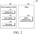
- FIG. 2 is a block diagram 200 illustrating the power management module 188 and the battery 189 according to various embodiments.
- the power management module 188 may include charging circuitry 210, a power adjuster 220, or a power gauge 230.
- the charging circuitry 210 may charge the battery 189 by using power supplied from an external power source outside the electronic device 101.
- the charging circuitry 210 may select a charging scheme (e.g., normal charging or quick charging) based at least in part on a type of the external power source (e.g., a power outlet, a USB, or wireless charging), magnitude of power suppliable from the external power source (e.g., about 20 Watt or more), or an attribute of the battery 189, and may charge the battery 189 using the selected charging scheme.
- the external power source may be connected with the electronic device 101, for example, directly via the connecting terminal 178 or wirelessly via the antenna module 197.
- the power adjuster 220 may generate a plurality of powers having different voltage levels or different current levels by adjusting a voltage level or a current level of the power supplied from the external power source or the battery 189.
- the power adjuster 220 may adjust the voltage level or the current level of the power supplied from the external power source or the battery 189 into a different voltage level or current level appropriate for each of some of the components included in the electronic device 101.
- the power adjuster 220 may be implemented in the form of a low drop out (LDO) regulator or a switching regulator.
- the power gauge 230 may measure use state information about the battery 189 (e.g., a capacity, a number of times of charging or discharging, a voltage, or a temperature of the battery 189).
- the power management module 188 may determine, using, for example, the charging circuitry 210, the power adjuster 220, or the power gauge 230, charging state information (e.g., lifetime, over voltage, low voltage, over current, over charge, over discharge, overheat, short, or swelling) related to the charging of the battery 189 based at least in part on the measured use state information about the battery 189.
- charging state information e.g., lifetime, over voltage, low voltage, over current, over charge, over discharge, overheat, short, or swelling
- the power management module 188 may determine whether the state of the battery 189 is normal or abnormal based at least in part on the determined charging state information. If the state of the battery 189 is determined to abnormal, the power management module 188 may adjust the charging of the battery 189 (e.g., reduce the charging current or voltage, or stop the charging).
- at least some of the functions of the power management module 188 may be performed by an external control device (e.g., the processor 120).
- the battery 189 may include a protection circuit module (PCM) 240.
- the PCM 240 may perform one or more of various functions (e.g., a pre-cutoff function) to prevent a performance deterioration of, or a damage to, the battery 189.
- the PCM 240 additionally or alternatively, may be configured as at least part of a battery management system (BMS) capable of performing various functions including cell balancing, measurement of battery capacity, count of a number of charging or discharging, measurement of temperature, or measurement of voltage.
- BMS battery management system
- At least a part of the use state information or the charging state information of the battery 189 may be measured using a corresponding sensor (e.g., a temperature sensor) among the sensor modules 176, the power gauge 230, or the power management module 188.
- the corresponding sensor e.g., the temperature sensor
- the corresponding sensor among the sensor modules 176 may be included as a part of the battery protection circuit module 240, or may be disposed in the vicinity of the battery 189 as a separate device.
- the power management module 188 may further include a power transmission circuit (for example, a power transmission circuit 311 of FIG. 3 ).
- the power transmission circuit 311 may include a power adapter configured to receive an input of a power source (or power) from the battery 189 and appropriately convert a voltage of the input power source, a power generation circuit configured to generate power, and/or a matching circuit configured to wirelessly transmit the generated power to an external electronic device (e.g., the electronic device 102 of FIG. 1 ).
- the power transmission circuit 311 may transmit the generated power to the external electronic device by maximizing the efficiency between a transmission coil and a reception coil of the external electronic device through the matching circuit.
- the electronic device may be one of various types of electronic devices.
- the electronic devices may include, for example, a portable communication device (e.g., a smartphone), a computer device, a portable multimedia device, a portable medical device, a camera, a wearable device, or a home appliance. According to an embodiment of the disclosure, the electronic devices are not limited to those described above.
- the electronic device may be a part of a plate-type/bar-type electronic device, a rollable electronic device, or a foldable electronic device. According to an embodiment of the disclosure, the electronic devices are not limited to those described above.
- each of such phrases as “A or B”, “at least one of A and B”, “at least one of A or B”, “A, B, or C”, “at least one of A, B, and C”, and “at least one of A, B, or C”, may include any one of, or all possible combinations of the items enumerated together in a corresponding one of the phrases.
- such terms as “1st” and “2nd”, or “first” and “second” may be used to simply distinguish a corresponding component from another, and does not limit the components in other aspect (e.g., importance or order).
- an element e.g., a first element
- the element may be coupled with the other element directly (e.g., wiredly), wirelessly, or via a third element.
- module may include a unit implemented in hardware, software, or firmware, and may interchangeably be used with other terms, for example, “logic”, “logic block”, “part”, or “circuitry”.
- a module may be a single integral component, or a minimum unit or part thereof, adapted to perform one or more functions.
- the module may be implemented in a form of an application-specific integrated circuit (ASIC).
- ASIC application-specific integrated circuit
- Various embodiments as set forth herein may be implemented as software (e.g., the program 140) including one or more instructions that are stored in a storage medium (e.g., internal memory 136 or external memory 138) that is readable by a machine (e.g., the electronic device 101).
- a processor e.g., the processor 120
- the one or more instructions may include a code generated by a complier or a code executable by an interpreter.
- the machine-readable storage medium may be provided in the form of a non-transitory storage medium.
- non-transitory simply means that the storage medium is a tangible device, and does not include a signal (e.g., an electromagnetic wave), but this term does not differentiate between where data is semi-permanently stored in the storage medium and where the data is temporarily stored in the storage medium.
- a method may be included and provided in a computer program product.
- the computer program product may be traded as a product between a seller and a buyer.
- the computer program product may be distributed in the form of a machine-readable storage medium (e.g., compact disc read only memory (CD-ROM)), or be distributed (e.g., downloaded or uploaded) online via an application store (e.g., PlayStoreTM), or between two user devices (e.g., smart phones) directly. If distributed online, at least part of the computer program product may be temporarily generated or at least temporarily stored in the machine-readable storage medium, such as memory of the manufacturer's server, a server of the application store, or a relay server.
- CD-ROM compact disc read only memory
- an application store e.g., PlayStoreTM
- two user devices e.g., smart phones
- each component e.g., a module or a program of the above-described components may include a single entity or multiple entities, and some of the multiple entities may be separately disposed in different components.
- one or more of the above-described components or operations may be omitted, or one or more other components or operations may be added.
- a plurality of components e.g., modules or programs
- the integrated component may still perform one or more functions of each of the plurality of components in the same or similar manner as they are performed by a corresponding one of the plurality of components before the integration.
- operations performed by the module, the program, or another component may be carried out sequentially, in parallel, repeatedly, or heuristically, or one or more of the operations may be executed in a different order or omitted, or one or more other operations may be added.
- FIG. 3 is a diagram illustrating a wireless charging system according to various embodiments.
- an electronic device 301 (for example, 102 of FIG. 1 ) (hereinafter also referred to as a "power transmission device”) according to various embodiments is configured to wirelessly supply power to an external electronic device 302 (for example, 101 of FIG. 1 ) (hereinafter also referred to as a "power reception device”), and the external electronic device 302 is configured to wirelessly receive power.
- an external electronic device 302 for example, 101 of FIG. 1
- the external electronic device 302 is configured to wirelessly receive power.
- the power transmission device 301 may correspond to a wireless power receiver or a power reception device.
- the power transmission device 301 may be applied to elements of the power reception device 302 required for power reception.
- the power transmission device 301 may include the power transmission circuit 311, a control circuit 312, a communication circuit 313, and/or a sensing circuit 314.
- the power transmission circuit 311 may include a power adapter 311a configured to receive an input of a power source (or power) from the outside and appropriately convert a voltage of the input power source, a power generation circuit 311b configured to generate power, and/or a matching circuit 311c configured to maximize the efficiency between a transmission coil 311L and a reception coil 321L.
- a power adapter 311a configured to receive an input of a power source (or power) from the outside and appropriately convert a voltage of the input power source
- a power generation circuit 311b configured to generate power
- a matching circuit 311c configured to maximize the efficiency between a transmission coil 311L and a reception coil 321L.
- the power transmission circuit 311 may include a plurality of at least a part of the power adapter 311a, the power generation circuit 311b, the transmission coil 311L, or the matching circuit 311c, so as to enable power transmission to a plurality of power reception devices (for example, a first external electronic device and a second external electronic device).
- the power generation circuit 311b may convert power received from the power adapter 311a into, for example, an alternating current waveform, and/or amplify and transfer the alternating current waveform to the transmission coil 311L.
- a frequency of the alternating current waveform may be configured to be about 100 to 205 kHz or about 6.78 MHz according to a standard, but is not limited thereto.
- the power generation circuit 311b may include an inverter.
- the inverter may be a full-bridge inverter or a half-bridge inverter, but the type of the inverter is not limited to these types of inverters.
- an induced magnetic field having a size which changes according to time may be formed from the transmission coil 311L, and thus the power may be wirelessly transmitted.
- at least one capacitor configuring a resonance circuit together with the transmission coil 311L may be further included in the power transmission circuit 311.
- the matching circuit 311c may change at least one of capacitance or reactance of a circuit connected to the transmission coil 311L under the control of the control circuit 312, so as to control the power transmission circuit 311 and a power reception circuit 321 to be impedance-matched with each other.
- an induced electromotive force may be generated by a magnetic field formed in the surroundings and having a size which changes according to time, and accordingly, the power reception circuit 321 may receive power wirelessly.
- the power transmission circuit 311 may support a plurality of power transmission schemes by using the power generation circuit 311b.
- the power transmission circuit 311 may transmit power by using a power transmission scheme suitable for an external electronic device among the plurality of power transmission schemes.
- the plurality of power transmission schemes may include a scheme of wirelessly transmitting power by using a magnetic induction scheme and/or a resonance induction scheme.
- the power transmission circuit 311 may use the power generation circuit 311b to generate signals of a first frequency band for providing a first power to a first external electronic device (for example, the power reception device 302) and signals of a second frequency band for providing a second power to a second external electronic device (not shown).
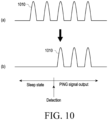
- the control circuit 312 may output a first signal (hereinafter also referred to as a "ping signal") for identifying approach of an external object in a ping phase (e.g., a standby power state) at each designated period through the transmission coil 311L in order to wirelessly transmit power, output a signal associated with authentication in an authentication state (identification & configuration phase), and output a second signal (power signal) for power transmission in a power transmission state (power transfer phase). That is, the control circuit 312 may output a first signal and a second signal of the first frequency band or the second frequency band according to each power transmission scheme. For example, the first frequency band and the second frequency band may be different from each other.
- control circuit 312 may perform the overall control of the power transmission device 301, and generate various messages required for wireless power transmission to transfer the messages to the communication circuit 313.
- the control circuit 312 may be implemented to be identical or similar to the processor 120 of FIG. 1 .
- the control circuit 312 may calculate power (or an amount of power) to be transmitted to the power reception device 302, based on information received from the communication circuit 313.
- the control circuit 312 may control the power transmission circuit 311 so that the power transmitted by the transmission coil 311L is transmitted to the power reception device 302.
- the control circuit 312 may control the power generation circuit 311b so as to generate a first signal and a second signal in a frequency band corresponding to each power transmission scheme.
- the communication circuit 313 may include at least one of a first communication circuit 313a and a second communication circuit 313b.
- the first communication circuit 313a may communicate with a first communication circuit 323a of the power reception device 302 by using, for example, a frequency which is the same as or adjacent to a frequency used for power transmission in the transmission coil 311L (e.g., an in-band scheme).
- the second communication circuit 323a may communicate with a second communication circuit 323b of the power reception device 302 by using, for example, a frequency which is different from a frequency used for power transmission in the transmission coil 311L (e.g., an out-band scheme).
- the second communication circuit 313b may use one of various short-range communication schemes, such as Bluetooth, BLE, Wi-Fi, and NFC, to obtain information (e.g., Vrec information, Iout information, various packets, a message, etc.) related to a charging state from the second communication circuit 323b.
- the first communication circuit 313a may be included in the power transmission circuit 311, and the first communication circuit 313a may communicate with the first communication circuit 323a of the power reception device 302.
- the sensing circuit 314 may include at least one sensor, and may detect at least one state of the power transmission device 301 by using the at least one sensor.
- the sensing circuit 314 may include at least one of a Hall sensor, a magnetic force sensor, a temperature sensor, a motion sensor, or a current (or voltage) sensor, and may identify a power transmission scheme of the power reception circuit 321 through the Hall sensor (or the magnetic force sensor), detect a temperature state of the power transmission device 301 by using the temperature sensor, detect a motion state of the power transmission device 301 by using the motion sensor, and detect a state of an output signal of the power transmission device 301, such as a current magnitude, a voltage magnitude, or a power magnitude, by using the current (or voltage) sensor.
- the current (or voltage) sensor may measure a signal in the power transmission circuit 311.
- a signal may be measured in at least a partial area of the transmission coil 311L, the matching circuit 311c, or the power generation circuit 311b.
- the current (or voltage) sensor may include a circuit configured to measure a signal at the front end of the transmission coil 311L.
- the sensing circuit 314 may measure a current and a voltage applied to the power transmission circuit 311 (e.g., the power generation circuit 311b or the transmission coil 311L) by a change of the power reception device 302, so as to detect a change in the power reception device 302.
- the power transmission circuit 311 e.g., the power generation circuit 311b or the transmission coil 311L
- the power reception device 302 may include the power reception circuit 321 (e.g., the power management module 188), a control circuit 322 (e.g., the processor 120), a communication circuit 323 (e.g., the communication module 190), at least one sensor 324 (e.g., the sensor module 176), or a display 325 (e.g., the display device 160).
- the description of the configuration corresponding to the power transmission device 301 may be partially omitted.
- the power reception device 302 may correspond to a wireless power transmitter or a power transmission device.
- the power reception device 302 may include elements of the power transmission device 301 required for power transmission.
- the power reception circuit 321 may include the reception coil 321L configured to wirelessly receive power from the power transmission device 301, a matching circuit 321a, a rectifier circuit 321b configured to rectify a received AC power to a DC, a regulating circuit 321c configured to regulate a charging voltage, a switch circuit 321d, and/or a battery 321e (e.g., the battery 189).
- control circuit 322 may perform the overall control of the power reception device 302, and generate various messages required for wireless power reception to transfer the messages to the communication circuit 323.
- the communication circuit 323 may include at least one of the first communication circuit 323a and the second communication circuit 323b.
- the first communication circuit 323a may communicate with the power transmission device 301 through the reception coil 321L.
- the second communication circuit 323b may communicate with the power transmission device 301 by using one of various short-range communication schemes such as Bluetooth, BLE, Wi-Fi, and NFC.
- the first communication circuit 323a may be included in the power reception circuit 321, and the first communication circuit 323a may communicate with the first communication circuit 313a of the power reception device 301.
- the display 325 may display various display information required for wireless power transmission/reception.
- the at least one sensor 324 may include at least a part of a current/voltage sensor, a temperature sensor, an illuminance sensor, or a sound sensor.
- the at least one sensor 324 may detect the power transmission device 301 by detecting a discovery signal or received power from the power transmission device 301.
- the at least one sensor 324 may detect a signal change of an input/output terminal of the rectifier circuit 321b, the matching circuit 321a, or the reception coil 321L, generated by a signal output from the power transmission device 301.
- the at least one sensor 324 may be included in the power reception circuit 321.
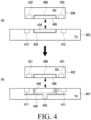
- FIG. 4 is a diagram illustrating a wireless charging system according to various embodiments.
- a power transmission device 403 may include a first magnetic element 430 having a first polarity (or a first pole).
- the power transmission device 403 may be disposed to be aligned with a power reception device 404 in order to wirelessly transmit power to the power reception device 404.
- the power transmission device 403 may use the first magnetic element 430 for placement for maximizing efficiency and/or minimizing the phenomenon of induction heating. That is, the first magnetic element 430 may be used so that the power transmission device 403 and the power reception device 404 are fixed at appropriate positions.
- a wireless charging coil 412 included in the power transmission device 403 may be disposed in an annular shape without a central portion thereof like a donut, and the first magnetic element 430 may be positioned in the central portion where the wireless charging coil 412 does not exist.
- the first magnetic element 430 may include a shielding member 435 in the surroundings thereof so as not to affect a magnetic force of the wireless charging coil 412.
- the power reception device 404 may include a second magnetic element 480 having a second polarity (or a second pole).
- a wireless charging coil 422 included in the power transmission device 404 may be disposed in an annular shape without a central portion thereof like a donut, and the second magnetic element 480 may be positioned in the central portion where the wireless charging coil 422 does not exist.
- the second magnetic element 480 may include a shielding member 485 in the surroundings thereof so as not to affect a magnetic force of the wireless charging coil 422.
- each of the power transmission device 403 and the power reception device 404 may include magnetic elements 430 and 480 having different polarities. For example, when the first polarity corresponds to an "N pole", the second polarity may correspond to an "S pole", and when the first polarity corresponds to an "S pole", the second polarity may correspond to an "N pole".
- the power transmission device 403 may be aligned at a position where power transmission efficiency is highest, due to an attractive force between the magnetic elements 430 and 480 and the power reception device 404 including a magnetic element having the second polarity opposite to the first polarity.
- the power transmission device 403 may not be aligned with the power reception device 404 due to a repulsive force between the magnetic elements 430 and 480 and the power reception device 404 including a magnetic element having the same polarity as the first polarity.
- a power transmission device 401 may include a first magnetic element 440 which can be rotated to have a first polarity or a second polarity in a first direction.
- a wireless charging coil 411 included in the power transmission device 401 may be disposed in an annular shape without a central portion thereof like a donut, and the rotatable first magnetic element 440 may be positioned in the central portion where the wireless charging coil 411 does not exist.
- the rotatable first magnetic element 440 may include a shielding member 445 in the surroundings thereof so as not to affect a magnetic force of the wireless charging coil 411.
- the shielding member 445 may include a hole so that the first magnetic element 440 may transfer a magnetic force to a Hall sensor 450 adjacent to the first magnetic element 440.
- at least a part of the shielding member 445 may be positioned in a second direction of the first magnetic element 440 and/or the wireless charging coil 411. The shielding member 445 may prevent at least a part of a magnetic force generated by a coil and/or a magnet from being affected in the second direction.
- the Hall sensor 450 may be positioned between the first magnetic element 440 and the shielding member 445.
- the Hall sensor 450 may be positioned in the second direction of the shielding member 445.
- the shielding member 445 may be positioned between the first magnetic element 440 and the Hall sensor 450.
- the shielding member 445 may include a hole so that the first magnetic element 440 may transfer a magnetic force to the Hall sensor 450 adjacent to the first magnetic element 440.
- the shielding member 445 may be implemented in a form which surrounds the first magnetic element 440.
- the shielding member 445 is shown to be extended up to an area between the wireless charging coil 411 and the Hall sensor 450 such that the Hall sensor 450 is not affected by the wireless charging coil 411, the technical idea of the disclosure may not be limited thereto.
- the shielding member 445 may be implemented in a form which surrounds only the first magnetic element 440.
- the power transmission device 401 may be positioned in parallel with a power reception device 402 by using the first magnetic element 440 for alignment.
- the first direction may refer to a direction facing the power reception device 402 when the power transmission device 401 wirelessly transmits power. That is, the first magnetic element 440 may rotate so as to have a polarity different from that of a second magnetic element 490 of the power reception device 402 in the first direction.
- a wireless charging coil 421 included in the power reception device 402 may be disposed in an annular shape without a central portion thereof like a donut, and the second magnetic element 490 may be positioned in the central portion where the wireless charging coil 421 does not exist.
- the second magnetic element 490 may include a shielding member 495 in the surroundings thereof so as not to affect a magnetic force of the wireless charging coil 421.
- the shielding member 495 may be positioned in the first direction of the wireless charging coil 421 and/or the second magnetic element 490.
- the power transmission device 401 when the power reception device 402 is in contact with the power transmission device 401, the power transmission device 401 may be disposed such that a polarity of the first magnetic element 440 of the power transmission device 401 is aligned according to a polarity of the second magnetic element 490 of the power reception device 402.
- the first magnetic element 440 When the second magnetic element 490 has the first polarity, the first magnetic element 440 may rotate in the first direction to have the second polarity opposite to the first polarity.
- the second magnetic element 490 has the second polarity, the first magnetic element 440 may rotate in the first direction to have the first polarity opposite to the second polarity.
- the power transmission device 401 may be disposed to be aligned with the power reception device 402 even when the power reception device 402 includes a magnetic element having any polarity, and thus wirelessly transmit power.
- the power transmission devices 401 and the power reception device 402 are different, power transmission between the two devices may not be possible, or power transmission efficiency may decrease even when the power transmission device 401 transmits power to the power reception device 402.
- the power reception device 402 may include a magnetic element having a different polarity for each manufacturer.
- the power reception device 402 may use a different power transmission scheme for each manufacturer (for example, a frequency of a signal for power transmission and/or a wireless power transmission communication protocol).
- the power transmission device 401 may identify a power transmission scheme of the power reception device 402, based on a polarity of the magnetic element 490 included in the power reception device 402. In this regard, hereinafter, a method of identifying a power transmission scheme of the power reception device 402 by the power transmission device 401 will be described in detail.
- the operations of the power transmission device 401 described below may be performed by a processor (the processor 120 of FIG. 1 ) or a control circuit (for example, the control circuit 312 of FIG. 3 ) included in the power transmission device 401. However, for convenience of description, it will be assumed that a subject of the operations is the power transmission device 401.
- FIG. 5 is a flowchart illustrating an operation of a power transmission device according to various embodiments.
- the power transmitter 401 identifies a polarity of the first magnetic element 440 and/or the second magnetic element 490 due to approach of an external electronic device (e.g., the power reception device 402 of FIG. 3 ).
- a first polarity of the first magnetic element 440 may be aligned in a first direction by a magnetic force generated when the second magnetic element 490 included in the external electronic device 402 approaches the first magnetic element 440.
- the power transmission device 401 may identify a change in a magnetic force as the first polarity of the first magnetic element 440 is aligned in the first direction, and identify the polarity of the first magnetic element 440 in response to the change in the magnetic force.
- the first polarity of the first magnetic element 440 in the first direction may be opposite to a polarity of the second magnetic element 490.
- a second polarity of the first magnetic element 440 in a second direction opposite to the first direction may be the same as the polarity of the second magnetic element 490.
- the power transmission device 401 may identify the second polarity of the first magnetic element 440 in the second direction in a state in which the first polarity of the first magnetic element 440 is aligned in the first direction, through a sensor (for example, a Hall sensor or a magnetic force sensor).
- the power transmission device 401 may identify the polarity of the second magnetic element 490, based on the second polarity of the first magnetic element 440 in the second direction.
- the sensor for example, a Hall sensor or a magnetic force sensor
- the sensor may be positioned in the second direction of the first magnetic element 440, but may not be limited thereto.
- the power transmission device 401 may detect a change in magnetic flux through the sensor (for example, a Hall sensor or a magnetic force sensor) when the external electronic device 402 approaches the power transmission device 401, and identify the polarity of the second magnetic element 490 included in the external electronic device 402, based on the detected state (or change) of the magnetic flux. For example, the power transmission device 401 may identify the polarity of the first magnetic element 440 and/or the second magnetic element 490, based on a direction of the magnetic flux. For example, the power transmission device 401 may identify a strength of a magnetic force, based on the density of magnetic flux (or the number of magnetic flux lines).
- the sensor for example, a Hall sensor or a magnetic force sensor
- the power transmission device 401 identifies a strength of a magnetic force.
- the power transmission device 401 may detect magnetic flux through the sensor (for example, a Hall sensor or a magnetic force sensor).
- the power transmission device 401 may identify the strength of the magnetic force, based on the magnetic flux detected through the sensor.
- the power transmission device 401 may compare the strength of the magnetic force with a threshold value.
- the power transmission device 401 may compare the strength of the magnetic force with the threshold value to identify whether the first magnetic element 440 is completely rotated to an "N pole" or an "S pole".
- the power transmission device 401 may identify whether the rotatable first magnetic element 440 malfunctions, through the operation of comparing the strength of the magnetic force with the threshold value.
- the sensor of the power transmission device 401 may identify that the power reception device 402 is located in the vicinity of the power transmission device 401, based on the detected strength of the magnetic force. For example, when the power reception device 402 is more than a predetermined distance away from the power transmission device 401, the sensor may detect a first magnetic force strength, and when the power reception device 402 is located in the vicinity of the power transmission device 401, the sensor may detect a second magnetic force strength. For example, the second magnetic force strength may be greater than the first magnetic force strength.
- the power transmission device 401 may be aware that the power reception device 402 is located in the vicinity of the power transmission device 401, based on the magnetic force strength.
- the power transmission device 401 determines one power transmission scheme among a plurality of power transmission schemes, based on the polarity of the magnetic element and the strength of the magnetic force. For example, each of the plurality of power transmission schemes may have a different frequency band of a signal for power transmission. In addition, each of the plurality of power transmission schemes may have a different resonant frequency of a signal for power transmission.
- the configuration of operation 503 may be omitted.
- the power transmission device 401 may determine one power transmission scheme among the plurality of power transmission schemes, based on the polarity of the magnetic element without measuring the strength of the magnetic force.
- the power transmission device 401 wirelessly transmits power to the external electronic device 402, based on the determined power transmission scheme.
- the power transmission device 401 may output a ping signal and a signal for power transmission, based on a frequency band and a resonant frequency corresponding to the determined power transmission scheme.
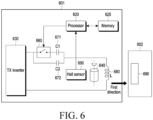
- FIG. 6 is a block diagram of a power transmission device according to various embodiments.
- a power transmission device 601 may include a processor 620, a memory 625, an inverter 630, a first magnetic element 640, a Hall sensor 650, a switch 660, a first capacitor 671, a second capacitor 672, and a coil 680.
- the power transmission device 601 may be implemented to be identical or similar to the electronic device 101 of FIG. 1 or the power transmission device 301 of FIG. 3 .
- the first magnetic element 640 may rotate to have a polarity of an "N pole” or an "S pole” in a first direction.
- the first magnetic element 640 may have an "N pole” on one surface thereof and have an "S pole” on the other surface thereof.
- the first direction may be a direction toward a power reception device 602.
- the power reception device 602 may include a second magnetic element 690.
- the second magnetic element 690 may have the polarity of the "N pole” or the "S pole".
- the second magnetic element 690 may have one polarity of the "N pole” and "S pole”.
- the second magnetic element 690 may be disposed to be fixed at a specific position of the power reception device 602.
- the expression of having one polarity may mean a magnet which performs only a role corresponding to a single pole in the embodiment disclosed herein.
- a single-pole magnet may be implemented in the following form.
- a magnet including the "N pole” and the "S pole” functions as a multi-pole magnet when placed along a surface of a housing (when placed parallel to the surface), but when the magnet including the "N pole” and the "S pole” is placed perpendicular to the surface of the housing, only a pole adjacent to the surface may function to generate a magnetic force (e.g., an attractive force) in relation to the power transmission device 601.
- a magnet having a polarity disposed perpendicular to the housing may be referred to as a single-pole magnet for convenience of description/distinction.
- a magnet having one polarity may be implemented as a magnet which physically includes two poles, but substantially has the one polarity which is overwhelmingly dominant.
- a magnet composite such as a Halbach array may function as a single-pole magnet.
- a magnet having one polarity may be implemented as a magnet with an appropriate shape/arrangement (e.g., a pot type and a ring type) manufactured in consideration of a situation in which only single-pole magnetism is required.
- an appropriate shape/arrangement e.g., a pot type and a ring type
- the second magnetic element 690 may have one polarity of the "N pole” and the "S pole", this is merely exemplary, and the number of polarities is not limited.
- each of the first magnetic element 640 and the second magnetic element 690 may include both the "N pole” and the "S pole".
- the "N poles” and the "S poles” of the first magnetic element 640 and the second magnetic element 690 may be arranged to cross each other.
- a plurality of first magnetic elements 640 and a plurality of second magnetic elements 690 may be disposed.
- the processor 620 may control the overall operation of the power transmission device 601.
- the processor 620 may be implemented to be identical or similar to the processor 120 of FIG. 1 or the control circuit 312 of FIG. 3 .
- the processor 620 may identify a polarity of the first magnetic element 640 corresponding to the magnetic force through the Hall sensor 650.
- the processor 620 may identify a polarity of the first magnetic element 640 in a second direction.
- the second direction may be a direction opposite to the first direction.
- the processor 620 may identify a strength of a magnetic force through the Hall sensor 650.
- the processor 620 may identify a magnetic flux state or change through the Hall sensor 650.
- the processor 620 may compare a threshold value stored in the memory 625 with the strength of the magnetic force.
- the processor 620 may determine one power transmission scheme among a plurality of power transmission schemes, based on a polarity and a strength of a magnetic force.
- each of the plurality of power transmission schemes may be a wireless power transmission scheme supported by the power transmission device 601.
- a ping signal, a data transfer scheme (for example, a packet format for charging configuration), and a power transmission signal have frequency bands and resonant frequencies.
- the processor 620 may output a signal for controlling the switch 660 to the switch 660 in order to determine a frequency corresponding to a power transmission scheme.
- the processor 620 may control the switch 660 to determine resonant frequencies of a power transmission signal and a ping signal. For example, when the switch 660 is short-circuited, the resonant frequency may be determined based on capacitance C1+C2 of the first capacitor 671 and the second capacitor 672. On the other hand, when the switch 660 is opened, the resonant frequency may be determined based on capacitance C2 of the second capacitor 672.
- the switch 660 functions to determine capacitance as C2 or C1+C2
- the technical idea of the disclosure may not be limited thereto.
- the switch 660 may function to connect a path including the first capacitor or the second capacitor 672 to a branch point of the TX inverter 630.
- the capacitance may be determined as C1 or C2 by the switch 660.
- the resonant frequency may be determined based on capacitance C1 or C2.
- the processor 620 may wirelessly transmit power to the power reception device 602, based on the determined power transmission scheme.
- the processor 620 may output a ping signal and a power transmission signal, based on the determined power transmission scheme.
- the processor 620 may transmit power, based on a first power transmission scheme among the plurality of power transmission schemes.
- the processor 620 may transmit power, based on a second power transmission scheme among the plurality of power transmission schemes.
- the first power transmission scheme may be different from the second power transmission scheme.
- a resonant frequency of the first power transmission scheme may be determined based on the capacitance C1+C2
- a resonant frequency of the second power transmission scheme may be determined based on the capacitance C2.
- the resonant frequency of the second power transmission scheme may be greater than the resonant frequency of the first power transmission scheme.
- a frequency band of the first power transmission scheme may be 100 to 140 kHz
- a frequency band of the second power transmission scheme may be 250 to 320 kHz.
- FIGS. 7A and 7B are diagrams illustrating a wireless charging system according to various embodiments.
- the power transmission device 601 may determine a power transmission scheme according to a polarity of a second magnetic element of the power reception device 602.
- the power transmission device 601 may transmit power, based on a first power transmission scheme among a plurality of power transmission schemes. For example, a resonant frequency of the first power transmission scheme may be determined based on capacitance C1+C2 of a first capacitor 771 and a second capacitor 772 and an inductance L of a coil 780.
- the power transmission device 601 may use a first communication protocol corresponding to the first power transmission scheme.
- the power transmission device 601 may transmit power, based on a second power transmission scheme among the plurality of power transmission schemes. For example, a resonant frequency of the second power transmission scheme may be determined based on capacitance C2 of the second capacitor 772 and the inductance L of the coil 780.
- the power transmission device 601 may use a second communication protocol corresponding to the second power transmission scheme.
- the power transmission device 601 may transmit power, based on a first power transmission scheme among a plurality of power transmission schemes. For example, a resonant frequency of the first power transmission scheme may be determined based on the capacitance C1+C2 of the first capacitor 771 and the second capacitor 772 and the inductance L of the coil 780.
- a resonant frequency of the first power transmission scheme may be determined based on the capacitance C1+C2 of the first capacitor 771 and the second capacitor 772 and the inductance L of the coil 780.
- the power transmission device 601 may transmit power, based on a second power transmission scheme among the plurality of power transmission schemes. For example, a resonant frequency of the second power transmission scheme may be determined based on the capacitance C2 of the second capacitor 772 and the inductance L of the coil 780.
- capacitors 7A and 7B Although only two capacitors are illustrated in FIGS. 7A and 7B for convenience of description, the number of capacitors may not be limited thereto.
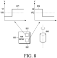
- FIG. 8 is a diagram illustrating an operation of determining a power transmission scheme through a sensor by a power transmission device according to various embodiments.
- the processor 620 may identify a polarity of a first magnetic element 840 (for example, the first magnetic element 640 of FIG. 6 ) through a Hall sensor 850 (e.g., the Hall sensor 650 of FIG. 6 ).
- the Hall sensor 850 (for example, the Hall sensor 650 of FIG. 6 ) may include a first sensor module 851 and a second sensor module 852.
- the first sensor module 851 may be a sensor for detecting a first pole (for example, an N pole)
- the second sensor module 852 may be a sensor for detecting a second pole (for example, an S pole).
- FIG. 8 illustrates the first sensor module 851 and the second sensor module 852 separately, the first sensor module 851 and the second sensor module 852 may be implemented as one sensor.
- the processor 620 may identify whether a polarity of the first magnetic element 840 toward the Hall sensor 850 corresponds to the first pole (for example, the N pole), through the first sensor module 851.
- the first sensor module 851 may output a voltage value 871, based on the polarity of the first magnetic element 840. For example, when the rotatable first magnetic element 840 completely faces the first pole (for example, the N pole) with reference to the Hall sensor 850, the first sensor module 851 may output a voltage value "V1" corresponding to a high level. For example, the voltage value "V1" may be greater than "VR1" indicating a first threshold value.
- the first sensor module 851 may output a voltage value lower than "VR1".
- the processor 620 may identify whether the polarity of the first magnetic element 840 toward the Hall sensor 850 corresponds to the second pole (for example, the S pole), through the second sensor module 852.
- the second sensor module 852 may output a voltage value 872, based on the polarity of the first magnetic element 840.
- the second sensor module 852 may output a voltage value "V2" corresponding to a high level.
- the voltage value "V2" may be greater than "VR2" indicating a second threshold value.
- the second sensor module 852 may output a voltage value lower than "VR2".
- the processor 620 may identify the polarity of the first magnetic element 840 and a strength of a magnetic force through the Hall sensor 850.
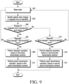
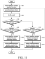
- FIG. 9 is a flowchart illustrating an operation of a power transmission device according to various embodiments.
- the power transmission device 601 (for example, the power transmission device of FIG. 6 ) may be in a sleep state.
- the sleep state may refer to a state in which a ping signal and/or a signal for power transmission is not output to the power reception device 602 (for example, the power reception device of FIG. 6 ).
- the power transmission device 601 may identify a polarity of the first magnetic element 640 (for example, the first magnetic element of FIG. 6 ), through the Hall sensor 650 (for example, the Hall sensor of FIG. 6 ). For example, when a change in a magnetic force is identified, the power transmission device 601 may switch from the sleep state to a wakeup state (or an active state). For example, the wakeup state (or active state) may be a state in which an operation for power transmission may be performed. In operation 905, the power transmission device 601 may identify whether the polarity of the first magnetic element 640 is an "N pole".
- operation 901 may be omitted.
- operation 903 may be directly performed.
- the power transmission device 601 may omit the operation of switching into the wakeup state (active state).
- the power transmission device 601 may identify the polarity of the first magnetic element 640 even when the change in the magnetic force is not identified.
- the power transmission device 601 may identify whether a magnetic force strength exceeds a first threshold value.
- the first threshold value may refer to a magnetic force strength when the rotatable first magnetic element 640 faces the "N pole" by a predetermined angle or more with reference to the Hall sensor 650.
- the power transmission device 601 may perform an operation of transmitting power to the power reception device 602, based on the first power transmission scheme. For example, the power transmission device 601 may transmit, to the power reception device 602, a power transmission signal having a resonant frequency corresponding to the first power transmission scheme. For example, when the specific packet is not received for a predetermined time, the power transmission device 601 may stop transmission of the power transmission signal and enter the sleep state again. Alternatively, when a packet indicating the completion of charging is received, the power transmission device 601 may stop transmission of the power transmission signal and enter the sleep state again.
- the power transmission device 601 may identify whether a magnetic force strength exceeds a second threshold value.
- the second threshold value may refer to a magnetic force strength when the rotatable first magnetic element 640 faces an "S pole" by a predetermined angle or more with reference to the Hall sensor 650.
- the second threshold value may be the same as or different from the first threshold value.
- the power transmission device 601 may enter the sleep state again without performing an operation for transmitting power.
- the power transmission device 601 may perform an operation of detecting the power reception device 602, based on a second power transmission scheme. For example, the power transmission device 601 may output a ping signal having a resonant frequency corresponding to the second power transmission scheme at a preconfigured period. For example, when a specific packet corresponding to the ping signal is received, the power transmission device 601 may perform an operation for power transmission. On the other hand, when the specific packet corresponding to the ping signal is not received, the power transmission device 601 may enter the sleep state again without performing the operation for power transmission.
- the power transmission device 601 may perform an operation of transmitting power to the power reception device 602, based on the second power transmission scheme. For example, the power transmission device 601 may transmit, to the power reception device 602, a power transmission signal having a resonant frequency corresponding to the second power transmission scheme. For example, when the specific packet is not received for a predetermined time, the power transmission device 601 may stop transmission of the power transmission signal and enter the sleep state again. Alternatively, when a packet indicating the completion of charging is received, the power transmission device 601 may stop transmission of the power transmission signal and enter the sleep state again.
- FIG. 10 is a diagram illustrating an operation of outputting a ping signal by a power transmission device according to various embodiments.
- a power transmission device may output a ping signal 1010 in order to detect a power reception device.
- the power transmission device according to the comparative embodiment may output the ping signal 1010 at a preconfigured period, based on a specific power transmission scheme.
- the power transmission device according to the comparative embodiment may output the ping signal 1010 until the power reception device is detected.
- the power transmission device 601 may not output the ping signal 1010 in a sleep state.
- the power transmission device 601 may output the ping signal 1010 at a preconfigured period, based on an operation (for example, a detection time point) of identifying a change in a magnetic force of the first magnetic element 640 (for example, the first magnetic element of FIG. 6 ).
- the power transmission device 601 may identify a polarity of the first magnetic element 640, through the Hall sensor 650 (for example, the Hall sensor of FIG. 6 ), and output the ping signal 1010, based on a power transmission scheme corresponding to the identified polarity. Accordingly, the power transmission device 601 can reduce power consumption when compared to case (a) of FIG. 10 .
- FIG. 11 is a flowchart illustrating an operation of a power transmission device according to various embodiments.
- the power transmission device 601 may output the first ping signal for a first designated time, and output the second ping signal for a second designated time.
- the power transmission device 601 may alternately output the first ping signal and the second ping signal within one time interval.
- the power transmission device 601 may detect a power reception device using the first power transmission scheme and/or a power reception device using the second power transmission scheme by alternately outputting the first ping signal and the second ping signal. That is, the power transmission device 601 may detect all the power reception devices using different power transmission schemes.
- the power transmission device 601 may identify a polarity of the first magnetic element 640 (for example, the first magnetic element of FIG. 6 ) through the Hall sensor 650 (for example, the Hall sensor of FIG. 6 ). For example, when a change in a magnetic force is identified, the power transmission device 601 may identify the polarity of the first magnetic element 640 (for example, the first magnetic element of FIG. 6 ) through the Hall sensor 650. Alternatively, the power transmission device 601 may also identify the polarity of the first magnetic element 640 (for example, the first magnetic element of FIG. 6 ), through the Hall sensor 650, without identifying a change in a magnetic force. For example, in operation 1105, the power transmission device 601 may identify whether the polarity of the first magnetic element 640 is an "N pole".
- the power transmission device 601 may identify whether a magnetic force strength exceeds a first threshold value.
- the first threshold value may refer to a magnetic force strength in a state in which the rotatable first magnetic element 640 is completely the "N pole" with reference to the Hall sensor 650.
- the power transmission device 601 may continuously output the first ping signal and the second ping signal without performing an operation for transmitting power.
- the power transmission device 601 may perform an operation of detecting the power reception device 602, based on the first power transmission scheme. For example, the power transmission device 601 may output a first ping signal having a resonant frequency corresponding to the first power transmission scheme at a preconfigured period. That is, the power transmission device 601 may output only the first ping signal. For example, when a specific packet corresponding to the first ping signal is received, the power transmission device 601 may perform an operation for power transmission. On the other hand, when the specific packet corresponding to the first ping signal is not received, the power transmission device 601 may output the first ping signal and the second ping signal again without performing the operation for power transmission.
- the power transmission device 601 may perform an operation of transmitting power to the power reception device 602, based on the first power transmission scheme. For example, the power transmission device 601 may transmit, to the power reception device 602, a power transmission signal having a resonant frequency corresponding to the first power transmission scheme. For example, when the specific packet is not received for a predetermined time, the power transmission device 601 may stop transmission of the power transmission signal and output the first ping signal and the second ping signal again. Alternatively, when a packet indicating the completion of charging is received, the power transmission device 601 may stop transmission of the power transmission signal and output the first ping signal and the second ping signal again.
- the power transmission device 601 may identify whether a magnetic force strength exceeds a second threshold value.
- the second threshold value may refer to a magnetic force strength in a state in which the rotatable first magnetic element 640 is completely an "S pole" with reference to the Hall sensor 650.
- the second threshold value may be the same as or different from the first threshold value.
- the power transmission device 601 may output the first ping signal and the second ping signal again without performing an operation for transmitting power.
- the power transmission device 601 may perform an operation of detecting the power reception device 602, based on the second power transmission scheme. For example, the power transmission device 601 may output a second ping signal having a resonant frequency corresponding to the second power transmission scheme at a preconfigured period. For example, when a specific packet corresponding to the second ping signal is received, the power transmission device 601 may perform an operation for power transmission. On the other hand, when the specific packet corresponding to the second ping signal is not received, the power transmission device 601 may output the first ping signal and the second ping signal again without performing the operation for power transmission.
- the power transmission device 601 may perform an operation of transmitting power to the power reception device 602, based on the second power transmission scheme. For example, the power transmission device 601 may transmit, to the power reception device 602, a power transmission signal having a resonant frequency corresponding to the second power transmission scheme. For example, when the specific packet is not received for a predetermined time, the power transmission device 601 may stop transmission of the power transmission signal and output the first ping signal and the second ping signal again. Alternatively, when a packet indicating the completion of charging is received, the power transmission device 601 may stop transmission of the power transmission signal and output the first ping signal and the second ping signal again.
- FIG. 12 is a diagram illustrating an operation of outputting ping signals by a power transmission device according to various embodiments.
- a power transmission device may output a first ping signal 1210 of a first power transmission scheme and a second ping signal 1220 of a second power transmission scheme in order to detect a power reception device.
- the power transmission device 601 may detect a power reception device using the first power transmission scheme and/or a power reception device using the second power transmission scheme by alternately outputting the first ping signal and the second ping signal. That is, the power transmission device 601 may alternately output the first ping signal and the second ping signal in order to detect all the power reception devices using different power transmission schemes.
- the power transmission device 601 may output one of the first ping signal 1210 and the second ping signal 1220 at a preconfigured period, based on an operation (for example, a detection time point) of identifying a change in a magnetic force of the first magnetic element 640 (for example, the first magnetic element of FIG. 6 ). For example, when the change in the magnetic force is identified, the power transmission device 601 may identify a polarity of the first magnetic element 640, through the Hall sensor 650 (for example, the Hall sensor of FIG. 6 ), and output the first ping signal 1210 or the second ping signal 1220, based on a power transmission scheme corresponding to the identified polarity.
- an operation for example, a detection time point
- the power transmission device 601 may identify a polarity of the first magnetic element 640, through the Hall sensor 650 (for example, the Hall sensor of FIG. 6 ), and output the first ping signal 1210 or the second ping signal 1220, based on a power transmission scheme corresponding to the identified
- the power transmission device 601 may output the first ping signal 1210 according to a preconfigured period.
- the power transmission device 601 may output the second ping signal 1220 according to a preconfigured period.
- the power transmission device 601 may output the first ping signal 1210 according to a preconfigured period.
- the power transmission device 601 may output the second ping signal 1220 according to a preconfigured period.
- An electronic device may include a sensor, a first magnetic element which can be rotated to have a polarity of a first pole or a second pole in a first direction, and a processor, wherein the processor is configured to, identify, based at least in part on the sensor, a polarity of a first magnetic element or a second magnetic element and a strength of a magnetic force generated by approaching of the second magnetic element to the first magnetic element, the polarity being determined by the magnetic force, the second magnetic element being included in an external electronic device, select a power transmission scheme from a plurality of power transmission schemes, based on the polarity and the strength of the magnetic force, and wirelessly transmit power to the external electronic device, based at least in part on the power transmission scheme.
- the processor may be configured to determine a frequency of a ping signal and a frequency of a power transmission signal, based on the power transmission scheme.
- the processor may be configured to output a signal for controlling a switch included in the electronic device, in order to determine the frequency of the ping signal and the frequency of the power transmission signal.
- Each of the plurality of power transmission schemes may have different resonant frequencies of a ping signal and a power transmission signal.
- the processor may be configured to, based on identifying that a polarity of the magnetic force corresponds to the first pole, perform an operation of transmitting the power, based on a first power transmission scheme, and based on identifying that the polarity of the magnetic force corresponds to the second pole, perform an operation of transmitting the power, based on a second power transmission scheme different from the first power transmission scheme.
- the processor may be configured to, based on identifying the magnetic force when the electronic device is in a sleep state, change the sleep state to an active state.
- the processor may be configured to compare the strength of the magnetic force with a threshold value and start an operation detecting the external electronic device based on a determination that the strength of the magnetic force is greater than the threshold value.
- the processor may be configured to output a ping signal having a frequency determined based on the power transmission scheme.
- the processor may be configured to, based on detecting the external electronic device, transmit a power transmission signal having a frequency determined based on the power transmission scheme to the external electronic device.
- the processor may be configured to compare the strength of the magnetic force with a threshold value, and based on a determination that the strength of the magnetic force is less than or equal to the threshold value, change the active state to the sleep state.
- An operating method of an electronic device including a first magnetic element which can be rotated to have a polarity of a first pole or a second pole in a first direction may include identifying a polarity of a first magnetic element or a second magnetic element and a strength of a magnetic force generated by approaching of the second magnetic element to the first magnetic element, the polarity being determined by the magnetic force, the second magnetic element being included in an external electronic device, determining a power transmission scheme among a plurality of power transmission schemes, based on the polarity and the strength of the magnetic force, and wirelessly transmitting power to the external electronic device, based on the power transmission scheme.
- the determining of the power transmission scheme may include determining a frequency of a ping signal and a frequency of a power transmission signal, based on the power transmission scheme.
- the determining of the power transmission scheme may include outputting a signal for controlling a switch included in the electronic device, in order to determine the frequency of the ping signal and the frequency of the power transmission signal.
- Each of the plurality of power transmission schemes may have different resonant frequencies of a ping signal and a power transmission signal.
- the operating method of the electronic device may further include, based on identifying the magnetic force when the electronic device is in a sleep state, changing the sleep state to an active state.
- the transmitting of the power may include comparing the strength of the magnetic force with a threshold value and detecting the external electronic device based on a determination that the strength of the magnetic force is greater than the threshold value.
- the transmitting of the power may include outputting a ping signal having a frequency corresponding to the power transmission scheme.
- the transmitting of the power may include, based on detecting the external electronic device, transmitting a power transmission signal having a frequency corresponding to the power transmission scheme to the external electronic device.
- the operating method of the electronic device may further include comparing the strength of the magnetic force with a threshold value, and based on a determination that the strength of the magnetic force is less than or equal to the threshold value, changing the active state to the sleep state.
- a computer-readable recording medium may store instructions configured to, when executed, cause a processor to: identify a polarity of a first magnetic element or a second magnetic element and a strength of a magnetic force generated by approaching of the second magnetic element to the first magnetic element, the polarity being determined by the magnetic force, the first magnetic element being included in an electronic device and being rotatable in a first direction to have a polarity of a first pole or a second pole, the second magnetic element being included in an external electronic device; determine a power transmission scheme among a plurality of power transmission schemes, based on the polarity and the strength of the magnetic force; and wirelessly transmit power to the external electronic device, based on the power transmission scheme.
- Each of the above-described elements of the electronic device may be configured by one or more components, and the name of the corresponding element may be changed according to the type of the electronic device.
- the electronic device may include at least one of the above-described elements, and some of the elements may be omitted from the electronic device, or other additional elements may be further included in the electronic device.
- some of the elements of the electronic device according to various embodiments may be combined with each other to configure one entity, thereby making it possible to perform the functions of the corresponding elements in the same manner as before the combination.
Landscapes
- Engineering & Computer Science (AREA)
- Computer Networks & Wireless Communication (AREA)
- Power Engineering (AREA)
- Charge And Discharge Circuits For Batteries Or The Like (AREA)
Claims (15)
- Elektronische Vorrichtung, die Folgendes umfasst:einen Sensor;ein erstes magnetisches Element, das gedreht werden kann, so dass es in einer ersten Richtung eine Polarität eines ersten Pols oder eines zweiten Pols aufweist; undeinen Prozessor,wobei der Prozessor zu Folgendem konfiguriert ist:identifizieren, basierend zumindest zum Teil auf dem Sensor, einer Polarität von einem aus einem ersten magnetischen Element und einem zweiten magnetischen Element sowie einer Stärke einer magnetischen Kraft, die durch Annäherung des zweiten magnetischen Elements an das erste magnetische Element erzeugt wird, wobei die Polarität durch die magnetische Kraft bestimmt wird, wobei das zweite magnetische Element in einer externen elektronischen Vorrichtung enthalten ist,Auswählen eines Stromübertragungsschemas aus einer Vielzahl von Stromübertragungsschemata, basierend zumindest zum Teil auf der Polarität und der Stärke der Magnetkraft, unddrahtloses Übertragen von Strom an die externe elektronische Vorrichtung, basierend auf dem Stromübertragungsschema.
- Elektronische Vorrichtung nach Anspruch 1, wobei der Prozessor zum Bestimmen einer Frequenz eines Ping-Signals und einer Frequenz eines Stromübertragungssignals, basierend auf dem Stromübertragungsschema, konfiguriert ist.
- Elektronische Vorrichtung nach Anspruch 2, wobei der Prozessor zum Ausgeben eines Signals zur Steuerung eines in der elektronischen Vorrichtung enthaltenen Schalters konfiguriert ist, um die Frequenz des Ping-Signals und die Frequenz des Stromübertragungssignals zu bestimmen.
- Elektronische Vorrichtung nach Anspruch 1, wobei jedes aus der Vielzahl von Stromübertragungsschemata unterschiedliche Resonanzfrequenzen bei einem Ping-Signal und einem Stromübertragungssignal aufweist.
- Elektronische Vorrichtung nach Anspruch 1, wobei der Prozessor zu Folgendem konfiguriert ist:basierend auf der Identifizierung, dass die Polarität der magnetischen Kraft dem ersten Pol entspricht, Durchführen einer Operation zum Übertragen des Stroms, basierend auf einem ersten Stromübertragungsschema, undbasierend auf der Identifizierung, dass die Polarität der magnetischen Kraft dem zweiten Pol entspricht, Durchführen einer Operation zum Übertragen des Stroms, basierend auf einem zweiten Stromübertragungsschema, das sich von dem ersten Stromübertragungsschema unterscheidet.
- Elektronische Vorrichtung nach Anspruch 1, wobei der Prozessor ferner konfiguriert ist, um basierend auf dem Identifizieren der magnetischen Kraft, wenn sich die elektronische Vorrichtung in einem Ruhezustand befindet, den Ruhezustand in einen aktiven Zustand zu ändern.
- Elektronische Vorrichtung nach Anspruch 1, wobei der Prozessor ferner konfiguriert ist, um die Stärke der magnetischen Kraft mit einem Schwellenwert zu vergleichen und eine Operation zum Erfassen der externen elektronischen Vorrichtung basierend auf einer Bestimmung zu starten, dass die Stärke der magnetischen Kraft größer als der Schwellenwert ist.
- Elektronische Vorrichtung nach Anspruch 7, wobei der Prozessor konfiguriert ist, um ein Ping-Signal mit einer basierend auf dem Stromübertragungsschema bestimmten Frequenz auszugeben.
- Elektronische Vorrichtung nach Anspruch 7, wobei der Prozessor ferner konfiguriert ist, um basierend auf dem Erfassen der externen elektronischen Vorrichtung ein Stromübertragungssignal mit einer basierend auf dem Stromübertragungsschema bestimmten Frequenz an die externe elektronische Vorrichtung zu übertragen.
- Elektronische Vorrichtung nach Anspruch 6, wobei der Prozessor ferner konfiguriert ist, um die Stärke der magnetischen Kraft mit einem Schwellenwert zu vergleichen und basierend auf einem Bestimmen, dass die Stärke der magnetischen Kraft kleiner oder gleich dem Schwellenwert ist, den aktiven Zustand in den Ruhezustand zu ändern.
- Betriebsverfahren einer elektronischen Vorrichtung, die ein erstes magnetisches Element umfasst, das gedreht werden kann, so dass es in einer ersten Richtung eine Polarität eines ersten Pols oder eines zweiten Pols aufweist, wobei das Verfahren Folgendes umfasst:Identifizieren einer Polarität von einem aus einem ersten magnetischen Element und einem zweiten magnetischen Element sowie einer Stärke einer magnetischen Kraft, die durch Annäherung des zweiten magnetischen Elements an das erste magnetische Element erzeugt wird, wobei die Polarität durch die magnetische Kraft bestimmt wird, wobei das zweite magnetische Element in einer externen elektronischen Vorrichtung enthalten ist,Auswählen eines Stromübertragungsschemas aus einer Vielzahl von Stromübertragungsschemata, basierend zumindest zum Teil auf der Polarität und der Stärke der Magnetkraft, unddrahtloses Übertragen von Strom an die externe elektronische Vorrichtung, basierend auf dem Stromübertragungsschema.
- Betriebsverfahren nach Anspruch 11, wobei das Bestimmen des Stromübertragungsschemas das Bestimmen einer Frequenz eines Ping-Signals und einer Frequenz eines Stromübertragungssignals, basierend auf dem Stromübertragungsschema, umfasst.
- Betriebsverfahren nach Anspruch 12, wobei das Bestimmen des Stromübertragungsschemas das Ausgeben eines Signals zur Steuerung eines in der elektronischen Vorrichtung enthaltenen Schalters umfasst, um die Frequenz des Ping-Signals und die Frequenz des Stromübertragungssignals zu bestimmen.
- Betriebsverfahren nach Anspruch 11, wobei jedes aus der Vielzahl von Stromübertragungsschemata unterschiedliche Resonanzfrequenzen bei einem Ping-Signal und einem Stromübertragungssignal aufweist.
- Betriebsverfahren nach Anspruch 11, ferner umfassend, basierend auf dem Identifizieren der magnetischen Kraft, wenn sich die elektronische Vorrichtung in einem Ruhezustand befindet, das Ändern des Ruhezustands in einen aktiven Zustand.
Applications Claiming Priority (2)
| Application Number | Priority Date | Filing Date | Title |
|---|---|---|---|
| KR1020200078631A KR102825251B1 (ko) | 2020-06-26 | 2020-06-26 | 무선으로 전력을 전송하는 전자 장치와 이의 동작 방법 |
| PCT/KR2021/005691 WO2021261759A1 (ko) | 2020-06-26 | 2021-05-06 | 무선으로 전력을 전송하는 전자 장치와 이의 동작 방법 |
Publications (3)
| Publication Number | Publication Date |
|---|---|
| EP4170866A1 EP4170866A1 (de) | 2023-04-26 |
| EP4170866A4 EP4170866A4 (de) | 2024-02-07 |
| EP4170866B1 true EP4170866B1 (de) | 2025-03-05 |
Family
ID=79281528
Family Applications (1)
| Application Number | Title | Priority Date | Filing Date |
|---|---|---|---|
| EP21828358.8A Active EP4170866B1 (de) | 2020-06-26 | 2021-05-06 | Elektronische vorrichtung zur drahtlosen stromübertragung und betriebsverfahren dafür |
Country Status (5)
| Country | Link |
|---|---|
| US (1) | US12062924B2 (de) |
| EP (1) | EP4170866B1 (de) |
| KR (1) | KR102825251B1 (de) |
| CN (1) | CN115917923B (de) |
| WO (1) | WO2021261759A1 (de) |
Families Citing this family (2)
| Publication number | Priority date | Publication date | Assignee | Title |
|---|---|---|---|---|
| CN214755753U (zh) * | 2021-05-13 | 2021-11-16 | 宁波微鹅电子科技有限公司 | 一种无线充电装置 |
| WO2024248365A1 (ko) * | 2023-05-26 | 2024-12-05 | 삼성전자 주식회사 | 전력을 무선으로 수신하는 전자 장치 및 그 동작 방법 |
Family Cites Families (21)
| Publication number | Priority date | Publication date | Assignee | Title |
|---|---|---|---|---|
| JP2007206776A (ja) | 2006-01-31 | 2007-08-16 | Seiko Epson Corp | 非接触電力伝送装置 |
| JP2008167582A (ja) | 2006-12-28 | 2008-07-17 | Toko Inc | 非接触電力伝送装置 |
| KR101606664B1 (ko) * | 2007-10-11 | 2016-03-25 | 퀄컴 인코포레이티드 | 자기 기계 시스템을 이용하는 무선 전력 전송 |
| WO2012036192A1 (ja) * | 2010-09-16 | 2012-03-22 | Necカシオモバイルコミュニケーションズ株式会社 | 非接触電力伝送機器 |
| KR101188808B1 (ko) | 2011-03-03 | 2012-10-09 | (주)엠에이피테크 | 단말기의 무선 충전장치 |
| WO2012152980A1 (en) * | 2011-05-06 | 2012-11-15 | Nokia Corporation | Method and apparatus for wireless charging |
| US9306399B2 (en) | 2011-05-12 | 2016-04-05 | Samsung Electronics Co., Ltd. | Wireless power transmission and charging system, and resonance frequency control method of wireless power transmission and charging system |
| KR20130075077A (ko) * | 2011-12-27 | 2013-07-05 | 삼성전기주식회사 | 무선 충전 장치 |
| JP2014023281A (ja) | 2012-07-18 | 2014-02-03 | Panasonic Corp | 伝送コイル装置及び携帯無線端末 |
| US9601267B2 (en) * | 2013-07-03 | 2017-03-21 | Qualcomm Incorporated | Wireless power transmitter with a plurality of magnetic oscillators |
| EP3061176B1 (de) * | 2013-10-24 | 2020-11-11 | Harald Merkel | Verfahren und anordnung zur drahtlosen energieübertragung |
| WO2015070321A1 (en) | 2013-11-13 | 2015-05-21 | Szeto Timothy Jing Yin | Magnetic connectors |
| US9912168B2 (en) | 2014-01-28 | 2018-03-06 | Lg Innotek Co., Ltd. | Wireless power transmitting apparatus and wireless power receiving apparatus |
| KR20160133140A (ko) * | 2015-05-12 | 2016-11-22 | 엘지이노텍 주식회사 | 무선 전력 송신 방법, 무선 전력 수신 방법 및 이를 위한 장치 |
| KR102483060B1 (ko) * | 2015-07-28 | 2023-01-03 | 삼성전자주식회사 | 무선 전력 송신기 |
| US10264341B2 (en) | 2017-01-20 | 2019-04-16 | Bose Corporation | Magnetic pivot sensor for headset microphone |
| KR102519193B1 (ko) * | 2017-09-29 | 2023-04-06 | 쓰리엠 이노베이티브 프로퍼티즈 캄파니 | 무선 전력 송신 장치와 이를 포함하는 무선 전력 시스템 |
| KR102480474B1 (ko) * | 2017-10-31 | 2022-12-23 | 삼성전자 주식회사 | 무선 전력을 수신하는 전자 장치 및 전자 장치의 동작 방법 |
| CN111742464A (zh) * | 2017-12-22 | 2020-10-02 | 无线先进车辆电气化有限公司 | 具有多个绕组的无线电力传输焊盘 |
| KR20200066118A (ko) * | 2018-11-30 | 2020-06-09 | 주식회사 노바텍 | 휴대기기용 무선충전장치 |
| US11070098B2 (en) * | 2019-01-16 | 2021-07-20 | Google Llc | Wireless charger with adaptive alignment assistance |
-
2020
- 2020-06-26 KR KR1020200078631A patent/KR102825251B1/ko active Active
-
2021
- 2021-05-06 EP EP21828358.8A patent/EP4170866B1/de active Active
- 2021-05-06 WO PCT/KR2021/005691 patent/WO2021261759A1/ko not_active Ceased
- 2021-05-06 CN CN202180045373.9A patent/CN115917923B/zh active Active
-
2022
- 2022-12-26 US US18/088,623 patent/US12062924B2/en active Active
Also Published As
| Publication number | Publication date |
|---|---|
| US20230126676A1 (en) | 2023-04-27 |
| US12062924B2 (en) | 2024-08-13 |
| KR102825251B1 (ko) | 2025-06-25 |
| WO2021261759A1 (ko) | 2021-12-30 |
| CN115917923A (zh) | 2023-04-04 |
| CN115917923B (zh) | 2025-08-08 |
| EP4170866A1 (de) | 2023-04-26 |
| KR20220000687A (ko) | 2022-01-04 |
| EP4170866A4 (de) | 2024-02-07 |
Similar Documents
| Publication | Publication Date | Title |
|---|---|---|
| US11862990B2 (en) | Wireless charging device and method for charging electronic device using the same | |
| US12062924B2 (en) | Electronic device for wireless power transmission and operating method thereof | |
| KR102871008B1 (ko) | 무선으로 전력을 송신하는 전자 장치와 무선으로 전력을 수신하는 무선 전력 수신 장치 및 그 동작 방법 | |
| US12444984B2 (en) | Method for controlling wireless charging mode and device therefor | |
| US20250183727A1 (en) | Electronic device and method supporting wireless charging using parallel switching structure | |
| US20230179028A1 (en) | Method for detecting foreign object and electronic device | |
| US12316154B2 (en) | Electronic device stabilizing output current of charging circuit and controlling method thereof | |
| EP4199306B1 (de) | Elektronische vorrichtung mit verbesserter drahtloser ladeeffizienz | |
| EP4318863A1 (de) | Elektronische vorrichtung zum laden einer batterie auf basis der innentemperatur | |
| KR102865543B1 (ko) | 충전 회로의 출력 전류를 안정화하는 전자 장치 및 그 제어 방법 | |
| US11843256B2 (en) | Wireless power transmission apparatus | |
| EP4601159A1 (de) | Elektronische vorrichtung zum drahtlosen empfangen von strom und betriebsverfahren dafür | |
| US20240195229A1 (en) | Electronic device for wireless charging in magnetic resonance type | |
| EP4325693A1 (de) | Elektronische vorrichtung und verfahren zum drahtlosen senden und empfangen von strom in einer elektronischen vorrichtung | |
| US20230062165A1 (en) | Electronic device and method of controlling wireless charging using the same | |
| KR102956426B1 (ko) | 무선 충전 방식을 제어하는 방법 및 그 장치 | |
| US20250267204A1 (en) | Case including shielding member and electronic device mounted thereon | |
| US20250364847A1 (en) | Electronic device including wireless charging device | |
| US20260066712A1 (en) | Electronic device and method of driving the same | |
| EP4418493A1 (de) | Elektronische vorrichtung zum drahtlosen empfangen von strom und betriebsverfahren dafür | |
| KR20250103298A (ko) | 무선으로 전력을 수신하는 전자 장치와 이의 동작 방법 | |
| KR20260037569A (ko) | 무선 전력을 송신하는 전자 장치 및 이를 이용한 무선 충전 방법 | |
| KR20240002106A (ko) | 무선으로 전력을 전송하는 전자 장치와 이의 동작 방법 | |
| KR20230060403A (ko) | 무선 전력 송신 장치 | |
| KR20240066024A (ko) | 차폐 부재를 포함하는 케이스 및 이에 장착된 전자 장치 |
Legal Events
| Date | Code | Title | Description |
|---|---|---|---|
| STAA | Information on the status of an ep patent application or granted ep patent |
Free format text: STATUS: THE INTERNATIONAL PUBLICATION HAS BEEN MADE |
|
| PUAI | Public reference made under article 153(3) epc to a published international application that has entered the european phase |
Free format text: ORIGINAL CODE: 0009012 |
|
| STAA | Information on the status of an ep patent application or granted ep patent |
Free format text: STATUS: REQUEST FOR EXAMINATION WAS MADE |
|
| 17P | Request for examination filed |
Effective date: 20230119 |
|
| AK | Designated contracting states |
Kind code of ref document: A1 Designated state(s): AL AT BE BG CH CY CZ DE DK EE ES FI FR GB GR HR HU IE IS IT LI LT LU LV MC MK MT NL NO PL PT RO RS SE SI SK SM TR |
|
| DAV | Request for validation of the european patent (deleted) | ||
| DAX | Request for extension of the european patent (deleted) | ||
| A4 | Supplementary search report drawn up and despatched |
Effective date: 20240108 |
|
| RIC1 | Information provided on ipc code assigned before grant |
Ipc: H02J 50/80 20160101ALI20240102BHEP Ipc: H02J 50/40 20160101ALI20240102BHEP Ipc: H02J 50/12 20160101ALI20240102BHEP Ipc: H02J 50/90 20160101AFI20240102BHEP |
|
| GRAP | Despatch of communication of intention to grant a patent |
Free format text: ORIGINAL CODE: EPIDOSNIGR1 |
|
| STAA | Information on the status of an ep patent application or granted ep patent |
Free format text: STATUS: GRANT OF PATENT IS INTENDED |
|
| INTG | Intention to grant announced |
Effective date: 20241011 |
|
| GRAS | Grant fee paid |
Free format text: ORIGINAL CODE: EPIDOSNIGR3 |
|
| GRAA | (expected) grant |
Free format text: ORIGINAL CODE: 0009210 |
|
| STAA | Information on the status of an ep patent application or granted ep patent |
Free format text: STATUS: THE PATENT HAS BEEN GRANTED |
|
| AK | Designated contracting states |
Kind code of ref document: B1 Designated state(s): AL AT BE BG CH CY CZ DE DK EE ES FI FR GB GR HR HU IE IS IT LI LT LU LV MC MK MT NL NO PL PT RO RS SE SI SK SM TR |
|
| REG | Reference to a national code |
Ref country code: GB Ref legal event code: FG4D |
|
| REG | Reference to a national code |
Ref country code: CH Ref legal event code: EP |
|
| REG | Reference to a national code |
Ref country code: IE Ref legal event code: FG4D |
|
| REG | Reference to a national code |
Ref country code: DE Ref legal event code: R096 Ref document number: 602021027280 Country of ref document: DE |
|
| REG | Reference to a national code |
Ref country code: NL Ref legal event code: FP |
|
| PGFP | Annual fee paid to national office [announced via postgrant information from national office to epo] |
Ref country code: NL Payment date: 20250422 Year of fee payment: 5 |
|
| PG25 | Lapsed in a contracting state [announced via postgrant information from national office to epo] |
Ref country code: RS Free format text: LAPSE BECAUSE OF FAILURE TO SUBMIT A TRANSLATION OF THE DESCRIPTION OR TO PAY THE FEE WITHIN THE PRESCRIBED TIME-LIMIT Effective date: 20250605 |
|
| PG25 | Lapsed in a contracting state [announced via postgrant information from national office to epo] |
Ref country code: FI Free format text: LAPSE BECAUSE OF FAILURE TO SUBMIT A TRANSLATION OF THE DESCRIPTION OR TO PAY THE FEE WITHIN THE PRESCRIBED TIME-LIMIT Effective date: 20250305 |
|
| PGFP | Annual fee paid to national office [announced via postgrant information from national office to epo] |
Ref country code: DE Payment date: 20250422 Year of fee payment: 5 |
|
| PG25 | Lapsed in a contracting state [announced via postgrant information from national office to epo] |
Ref country code: ES Free format text: LAPSE BECAUSE OF FAILURE TO SUBMIT A TRANSLATION OF THE DESCRIPTION OR TO PAY THE FEE WITHIN THE PRESCRIBED TIME-LIMIT Effective date: 20250305 |
|
| REG | Reference to a national code |
Ref country code: LT Ref legal event code: MG9D |
|
| PG25 | Lapsed in a contracting state [announced via postgrant information from national office to epo] |
Ref country code: NO Free format text: LAPSE BECAUSE OF FAILURE TO SUBMIT A TRANSLATION OF THE DESCRIPTION OR TO PAY THE FEE WITHIN THE PRESCRIBED TIME-LIMIT Effective date: 20250605 |
|
| PG25 | Lapsed in a contracting state [announced via postgrant information from national office to epo] |
Ref country code: HR Free format text: LAPSE BECAUSE OF FAILURE TO SUBMIT A TRANSLATION OF THE DESCRIPTION OR TO PAY THE FEE WITHIN THE PRESCRIBED TIME-LIMIT Effective date: 20250305 |
|
| PG25 | Lapsed in a contracting state [announced via postgrant information from national office to epo] |
Ref country code: LV Free format text: LAPSE BECAUSE OF FAILURE TO SUBMIT A TRANSLATION OF THE DESCRIPTION OR TO PAY THE FEE WITHIN THE PRESCRIBED TIME-LIMIT Effective date: 20250305 |
|
| PG25 | Lapsed in a contracting state [announced via postgrant information from national office to epo] |
Ref country code: BG Free format text: LAPSE BECAUSE OF FAILURE TO SUBMIT A TRANSLATION OF THE DESCRIPTION OR TO PAY THE FEE WITHIN THE PRESCRIBED TIME-LIMIT Effective date: 20250305 Ref country code: GR Free format text: LAPSE BECAUSE OF FAILURE TO SUBMIT A TRANSLATION OF THE DESCRIPTION OR TO PAY THE FEE WITHIN THE PRESCRIBED TIME-LIMIT Effective date: 20250606 |
|
| REG | Reference to a national code |
Ref country code: AT Ref legal event code: MK05 Ref document number: 1773868 Country of ref document: AT Kind code of ref document: T Effective date: 20250305 |
|
| PG25 | Lapsed in a contracting state [announced via postgrant information from national office to epo] |
Ref country code: SE Free format text: LAPSE BECAUSE OF FAILURE TO SUBMIT A TRANSLATION OF THE DESCRIPTION OR TO PAY THE FEE WITHIN THE PRESCRIBED TIME-LIMIT Effective date: 20250305 |
|
| PG25 | Lapsed in a contracting state [announced via postgrant information from national office to epo] |
Ref country code: SM Free format text: LAPSE BECAUSE OF FAILURE TO SUBMIT A TRANSLATION OF THE DESCRIPTION OR TO PAY THE FEE WITHIN THE PRESCRIBED TIME-LIMIT Effective date: 20250305 |
|
| PG25 | Lapsed in a contracting state [announced via postgrant information from national office to epo] |
Ref country code: PT Free format text: LAPSE BECAUSE OF FAILURE TO SUBMIT A TRANSLATION OF THE DESCRIPTION OR TO PAY THE FEE WITHIN THE PRESCRIBED TIME-LIMIT Effective date: 20250707 |
|
| PG25 | Lapsed in a contracting state [announced via postgrant information from national office to epo] |
Ref country code: IT Free format text: LAPSE BECAUSE OF FAILURE TO SUBMIT A TRANSLATION OF THE DESCRIPTION OR TO PAY THE FEE WITHIN THE PRESCRIBED TIME-LIMIT Effective date: 20250305 Ref country code: PL Free format text: LAPSE BECAUSE OF FAILURE TO SUBMIT A TRANSLATION OF THE DESCRIPTION OR TO PAY THE FEE WITHIN THE PRESCRIBED TIME-LIMIT Effective date: 20250305 |
|
| PG25 | Lapsed in a contracting state [announced via postgrant information from national office to epo] |
Ref country code: AT Free format text: LAPSE BECAUSE OF FAILURE TO SUBMIT A TRANSLATION OF THE DESCRIPTION OR TO PAY THE FEE WITHIN THE PRESCRIBED TIME-LIMIT Effective date: 20250305 |
|
| PG25 | Lapsed in a contracting state [announced via postgrant information from national office to epo] |
Ref country code: CZ Free format text: LAPSE BECAUSE OF FAILURE TO SUBMIT A TRANSLATION OF THE DESCRIPTION OR TO PAY THE FEE WITHIN THE PRESCRIBED TIME-LIMIT Effective date: 20250305 Ref country code: EE Free format text: LAPSE BECAUSE OF FAILURE TO SUBMIT A TRANSLATION OF THE DESCRIPTION OR TO PAY THE FEE WITHIN THE PRESCRIBED TIME-LIMIT Effective date: 20250305 |
|
| PG25 | Lapsed in a contracting state [announced via postgrant information from national office to epo] |
Ref country code: RO Free format text: LAPSE BECAUSE OF FAILURE TO SUBMIT A TRANSLATION OF THE DESCRIPTION OR TO PAY THE FEE WITHIN THE PRESCRIBED TIME-LIMIT Effective date: 20250305 |
|
| PG25 | Lapsed in a contracting state [announced via postgrant information from national office to epo] |
Ref country code: SK Free format text: LAPSE BECAUSE OF FAILURE TO SUBMIT A TRANSLATION OF THE DESCRIPTION OR TO PAY THE FEE WITHIN THE PRESCRIBED TIME-LIMIT Effective date: 20250305 |
|
| PG25 | Lapsed in a contracting state [announced via postgrant information from national office to epo] |
Ref country code: IS Free format text: LAPSE BECAUSE OF FAILURE TO SUBMIT A TRANSLATION OF THE DESCRIPTION OR TO PAY THE FEE WITHIN THE PRESCRIBED TIME-LIMIT Effective date: 20250705 |
|
| REG | Reference to a national code |
Ref country code: DE Ref legal event code: R097 Ref document number: 602021027280 Country of ref document: DE |
|
| REG | Reference to a national code |
Ref country code: CH Ref legal event code: H13 Free format text: ST27 STATUS EVENT CODE: U-0-0-H10-H13 (AS PROVIDED BY THE NATIONAL OFFICE) Effective date: 20251223 |
|
| PLBE | No opposition filed within time limit |
Free format text: ORIGINAL CODE: 0009261 |
|
| STAA | Information on the status of an ep patent application or granted ep patent |
Free format text: STATUS: NO OPPOSITION FILED WITHIN TIME LIMIT |
|
| PG25 | Lapsed in a contracting state [announced via postgrant information from national office to epo] |
Ref country code: DK Free format text: LAPSE BECAUSE OF FAILURE TO SUBMIT A TRANSLATION OF THE DESCRIPTION OR TO PAY THE FEE WITHIN THE PRESCRIBED TIME-LIMIT Effective date: 20250305 |
|
| REG | Reference to a national code |
Ref country code: CH Ref legal event code: L10 Free format text: ST27 STATUS EVENT CODE: U-0-0-L10-L00 (AS PROVIDED BY THE NATIONAL OFFICE) Effective date: 20260114 |
|
| PG25 | Lapsed in a contracting state [announced via postgrant information from national office to epo] |
Ref country code: LU Free format text: LAPSE BECAUSE OF NON-PAYMENT OF DUE FEES Effective date: 20250506 |
|
| PG25 | Lapsed in a contracting state [announced via postgrant information from national office to epo] |
Ref country code: CH Free format text: LAPSE BECAUSE OF NON-PAYMENT OF DUE FEES Effective date: 20250531 |
|
| REG | Reference to a national code |
Ref country code: BE Ref legal event code: MM Effective date: 20250531 |
|
| PG25 | Lapsed in a contracting state [announced via postgrant information from national office to epo] |
Ref country code: MC Free format text: LAPSE BECAUSE OF FAILURE TO SUBMIT A TRANSLATION OF THE DESCRIPTION OR TO PAY THE FEE WITHIN THE PRESCRIBED TIME-LIMIT Effective date: 20250305 |
|
| 26N | No opposition filed |
Effective date: 20251208 |
|
| GBPC | Gb: european patent ceased through non-payment of renewal fee |
Effective date: 20250605 |
|
| PG25 | Lapsed in a contracting state [announced via postgrant information from national office to epo] |
Ref country code: GB Free format text: LAPSE BECAUSE OF NON-PAYMENT OF DUE FEES Effective date: 20250605 |
|
| PG25 | Lapsed in a contracting state [announced via postgrant information from national office to epo] |
Ref country code: IE Free format text: LAPSE BECAUSE OF NON-PAYMENT OF DUE FEES Effective date: 20250506 |
|
| PG25 | Lapsed in a contracting state [announced via postgrant information from national office to epo] |
Ref country code: BE Free format text: LAPSE BECAUSE OF NON-PAYMENT OF DUE FEES Effective date: 20250531 |
|
| PG25 | Lapsed in a contracting state [announced via postgrant information from national office to epo] |
Ref country code: FR Free format text: LAPSE BECAUSE OF NON-PAYMENT OF DUE FEES Effective date: 20250531 |