EP4167487A1 - Low power quadrature phase detector - Google Patents
Low power quadrature phase detector Download PDFInfo
- Publication number
- EP4167487A1 EP4167487A1 EP22186206.3A EP22186206A EP4167487A1 EP 4167487 A1 EP4167487 A1 EP 4167487A1 EP 22186206 A EP22186206 A EP 22186206A EP 4167487 A1 EP4167487 A1 EP 4167487A1
- Authority
- EP
- European Patent Office
- Prior art keywords
- clock signal
- switch
- node
- transistor
- electrode
- Prior art date
- Legal status (The legal status is an assumption and is not a legal conclusion. Google has not performed a legal analysis and makes no representation as to the accuracy of the status listed.)
- Pending
Links
Images




Classifications
-
- H—ELECTRICITY
- H03—ELECTRONIC CIRCUITRY
- H03L—AUTOMATIC CONTROL, STARTING, SYNCHRONISATION OR STABILISATION OF GENERATORS OF ELECTRONIC OSCILLATIONS OR PULSES
- H03L7/00—Automatic control of frequency or phase; Synchronisation
- H03L7/06—Automatic control of frequency or phase; Synchronisation using a reference signal applied to a frequency- or phase-locked loop
- H03L7/08—Details of the phase-locked loop
- H03L7/0802—Details of the phase-locked loop the loop being adapted for reducing power consumption
-
- H—ELECTRICITY
- H03—ELECTRONIC CIRCUITRY
- H03D—DEMODULATION OR TRANSFERENCE OF MODULATION FROM ONE CARRIER TO ANOTHER
- H03D13/00—Circuits for comparing the phase or frequency of two mutually-independent oscillations
-
- H—ELECTRICITY
- H03—ELECTRONIC CIRCUITRY
- H03D—DEMODULATION OR TRANSFERENCE OF MODULATION FROM ONE CARRIER TO ANOTHER
- H03D3/00—Demodulation of angle-, frequency- or phase- modulated oscillations
- H03D3/007—Demodulation of angle-, frequency- or phase- modulated oscillations by converting the oscillations into two quadrature related signals
- H03D3/009—Compensating quadrature phase or amplitude imbalances
-
- H—ELECTRICITY
- H03—ELECTRONIC CIRCUITRY
- H03K—PULSE TECHNIQUE
- H03K17/00—Electronic switching or gating, i.e. not by contact-making and –breaking
- H03K17/51—Electronic switching or gating, i.e. not by contact-making and –breaking characterised by the components used
- H03K17/56—Electronic switching or gating, i.e. not by contact-making and –breaking characterised by the components used by the use, as active elements, of semiconductor devices
- H03K17/687—Electronic switching or gating, i.e. not by contact-making and –breaking characterised by the components used by the use, as active elements, of semiconductor devices the devices being field-effect transistors
-
- H—ELECTRICITY
- H03—ELECTRONIC CIRCUITRY
- H03L—AUTOMATIC CONTROL, STARTING, SYNCHRONISATION OR STABILISATION OF GENERATORS OF ELECTRONIC OSCILLATIONS OR PULSES
- H03L7/00—Automatic control of frequency or phase; Synchronisation
- H03L7/06—Automatic control of frequency or phase; Synchronisation using a reference signal applied to a frequency- or phase-locked loop
- H03L7/07—Automatic control of frequency or phase; Synchronisation using a reference signal applied to a frequency- or phase-locked loop using several loops, e.g. for redundant clock signal generation
-
- H—ELECTRICITY
- H03—ELECTRONIC CIRCUITRY
- H03L—AUTOMATIC CONTROL, STARTING, SYNCHRONISATION OR STABILISATION OF GENERATORS OF ELECTRONIC OSCILLATIONS OR PULSES
- H03L7/00—Automatic control of frequency or phase; Synchronisation
- H03L7/06—Automatic control of frequency or phase; Synchronisation using a reference signal applied to a frequency- or phase-locked loop
- H03L7/08—Details of the phase-locked loop
- H03L7/085—Details of the phase-locked loop concerning mainly the frequency- or phase-detection arrangement including the filtering or amplification of its output signal
- H03L7/087—Details of the phase-locked loop concerning mainly the frequency- or phase-detection arrangement including the filtering or amplification of its output signal using at least two phase detectors or a frequency and phase detector in the loop
-
- H—ELECTRICITY
- H03—ELECTRONIC CIRCUITRY
- H03L—AUTOMATIC CONTROL, STARTING, SYNCHRONISATION OR STABILISATION OF GENERATORS OF ELECTRONIC OSCILLATIONS OR PULSES
- H03L7/00—Automatic control of frequency or phase; Synchronisation
- H03L7/06—Automatic control of frequency or phase; Synchronisation using a reference signal applied to a frequency- or phase-locked loop
- H03L7/08—Details of the phase-locked loop
- H03L7/085—Details of the phase-locked loop concerning mainly the frequency- or phase-detection arrangement including the filtering or amplification of its output signal
- H03L7/091—Details of the phase-locked loop concerning mainly the frequency- or phase-detection arrangement including the filtering or amplification of its output signal the phase or frequency detector using a sampling device
-
- H—ELECTRICITY
- H03—ELECTRONIC CIRCUITRY
- H03L—AUTOMATIC CONTROL, STARTING, SYNCHRONISATION OR STABILISATION OF GENERATORS OF ELECTRONIC OSCILLATIONS OR PULSES
- H03L7/00—Automatic control of frequency or phase; Synchronisation
- H03L7/06—Automatic control of frequency or phase; Synchronisation using a reference signal applied to a frequency- or phase-locked loop
- H03L7/08—Details of the phase-locked loop
- H03L7/10—Details of the phase-locked loop for assuring initial synchronisation or for broadening the capture range
- H03L7/107—Details of the phase-locked loop for assuring initial synchronisation or for broadening the capture range using a variable transfer function for the loop, e.g. low pass filter having a variable bandwidth
-
- G—PHYSICS
- G01—MEASURING; TESTING
- G01R—MEASURING ELECTRIC VARIABLES; MEASURING MAGNETIC VARIABLES
- G01R25/00—Arrangements for measuring phase angle between a voltage and a current or between voltages or currents
- G01R25/005—Circuits for comparing several input signals and for indicating the result of this comparison, e.g. equal, different, greater, smaller, or for passing one of the input signals as output signal
-
- H—ELECTRICITY
- H03—ELECTRONIC CIRCUITRY
- H03D—DEMODULATION OR TRANSFERENCE OF MODULATION FROM ONE CARRIER TO ANOTHER
- H03D2200/00—Indexing scheme relating to details of demodulation or transference of modulation from one carrier to another covered by H03D
- H03D2200/0041—Functional aspects of demodulators
- H03D2200/0082—Quadrature arrangements
Definitions
- a quadrature phase detector is usually provided to detect a phase difference between an in-phase clock signal and a quadrature clock signal, and a detection result of the quadrature phase detector may be used by a clock signal generator or a delay element to adjust the phase of the in-phase clock signal or the quadrature clock signal.
- the conventional quadrature phase detector is usually implemented by using active devices such as XOR gates, however, using XOR gates may increase the power consumption.
- the quadrature phase detector is designed to detect four clock signals whose phases are 0 degree, 90 degrees, 180 degrees and 270 degrees
- four sets of circuits are designed to detect the phase difference between clock signals with 0 degree and 90 degrees, the phase difference between clock signals with 90 degrees and 180 degrees, the phase difference between clock signals with 180 degrees and 270 degrees, and the phase difference between clock signals with 270 degrees and 0 degree.
- a quadrature phase detector comprising a detection circuit.
- the detection circuit comprises a first switch, a second switch and a first filter, wherein the first switch is controlled by a second clock signal to selectively couple a first clock signal to a first node, the second switch is controlled by the second clock signal to selectively coupled the first node to a reference voltage, and the first filter is configured to filter voltages at the first node to generate a first detection result.
- a circuitry comprising a clock signal generator, a detection circuit and a control circuit.
- the clock signal generator is configured to generate a first clock signal and a second clock signal.
- the detection circuit comprises a first switch, a second switch and a first filter, wherein the first switch is controlled by a second clock signal to selectively couple a first clock signal to a first node, the second switch is controlled by the second clock signal to selectively coupled the first node to a reference voltage, and the first filter is configured to filter voltages at the first node to generate a first detection result.
- the control circuit is configured to generate a control signal to adjust a phase of the first clock signal or the second clock signal according to the first detection result.
- FIG. 1 is a diagram illustrating a circuitry 100 according to one embodiment of the present invention.
- the circuitry 100 comprises a quadrature phase detector 110, a control circuit 120 and a clock signal generator 130, wherein the quadrature phase detector 110 comprises a first detection circuit 112, a second detection circuit 114, a third detection circuit 116 and a fourth detection circuit 118.
- the circuitry 100 is configured to generate four clock signals CK0, CK90, CK180 and CK270 with ideal phases of 0 degree, 90 degrees, 180 degrees and 270 degrees, respectively.
- the quadrature phase detector 110 is configured to detect phase differences between any two adjacent clock signals to generate detection results.
- the first detection circuit 112 is configured to detect a phase difference between the clock signals CK0 and CK90 to generate a first detection result V1
- the second detection circuit 114 is configured to detect a phase difference between the clock signals CK90 and CK180 to generate a second detection result V2
- the third detection circuit 116 is configured to detect a phase difference between the clock signals CK180 and CK270 to generate a third detection result V3
- the fourth detection circuit 118 is configured to detect a phase difference between the clock signals CK270 and CK0 to generate a fourth detection result V4.
- the control circuit 120 refers to the first detection result V1, the second detection result V2, the third detection result V3 and the fourth detection result V4 to determine if any one of the clock signals CK0 CK90, CK180 and CK270 needs to adjust the phase, and at least one control signal Vc is generated accordingly.
- the control circuit 120 can refer to the first detection result V1 to determine if the phase difference between the clock signals CK0 and CK90 is not equal to 90 degrees, and to generate the control signal Vc to the clock signal generator 130 to adjust the phase of the clock signal CK90.
- the control circuit 120 can refer to the second detection result V2 to determine if the phase difference between the clock signals CK90 and CK180 is not equal to 90 degrees, and to generate the control signal Vc to the clock signal generator 130 to adjust the phase of the clock signal CK180.
- the control circuit 120 can refer to the third detection result V3 to determine if the phase difference between the clock signals CK180 and CK270 is not equal to 90 degrees, and to generate the control signal Vc to the clock signal generator 130 to adjust the phase of the clock signal CK270.
- the control circuit 120 can refer to the fourth detection result V4 to determine if the phase difference between the clock signals CK270 and CK0 is not equal to 90 degrees, and to generate the control signal Vc to the clock signal generator 130 to adjust the phase of the clock signal CK0.
- At least a portion of the first detection circuit 112, the second detection circuit 114 and the third detection circuit 116 and the fourth detection circuit 118 are designed so that most of the components are implemented by using passive components, to lower power consumption and improve the phase detection mismatches.
- FIG. 2 is a diagram illustrating the first detection circuit 112 according to one embodiment of the present invention.
- the first detection circuit 112 comprises transistors M11, M12, resistors R11, R12 and a low-pass filter 210, wherein the low-pass filter 210 comprises a resistor R13 and a capacitor C11.
- the transistor M11 is a P-type transistor while the transistor M12 is an N-type transistor, a gate electrode of the transistor M11 is coupled to the clock signal CK90, a first electrode of the M11 is coupled to a first electrode of the transistor M12 via the node N1 and the resistor R12, a second electrode of the transistor M11 is coupled to the clock signal CK0 via the resistor R11, and a second electrode of the transistor M12 is coupled to a ground voltage.
- the transistor M11 can be replaced by a switch with any different type, and this switch is controlled by the clock signal CK90 to selectively connect the clock signal CK0 to the node N1.
- the transistor M12 can be replaced by a switch with any different type, and this switch is controlled by the clock signal CK90 to selectively connect the node N1 to the ground voltage.
- the node N1 will have the high voltage (e.g. VDD); when both the clock signals CK90 and CK0 have the low voltage, the node N1 will have the low voltage; and when the clock signal CK90 has the high voltage, the node N1 will always have the low voltage because the transistor M12 with larger driving ability discharges the node N1.
- the first detection result V1 generated by filtering the voltage of the node N1 should be equal to (1/4)*VDD if the phase difference between the clock signals CK0 and CK90 is exactly equal to 90 degrees.
- the control circuit 120 may generate the control signal Vc to control the clock signal generator 130 to delay the phase of the clock signal CK90.
- the first detection result V1 is greater than (1/4)*VDD, it means that the phase difference between the clock signals CK0 and CK90 is greater than 90 degrees, and the control circuit 120 may generate the control signal Vc to control the clock signal generator 130 to advance the phase of the clock signal CK90.
- the first detection circuit 112 is configured to detect the phase difference based on rising edges of the clock signals CK0 and CK90.
- the transistor M11 may be implemented by an N-type transistor while the transistor M12 is implemented by the P-type transistor, for detecting the phase difference based on falling edges of the clock signals CK0 and CK90.
- FIG. 3 is a diagram illustrating the second detection circuit 114 according to one embodiment of the present invention.
- the second detection circuit 114 comprises transistors M21, M22, resistors R21, R22 and a low-pass filter 310, wherein the low-pass filter 310 comprises a resistor R23 and a capacitor C21.
- the transistor M21 is a P-type transistor while the transistor M22 is an N-type transistor, a gate electrode of the transistor M21 is coupled to the clock signal CK180, a first electrode of the M21 is coupled to a first electrode of the transistor M22 via the node N2 and the resistor R22, a second electrode of the transistor M21 is coupled to the clock signal CK90 via the resistor R21, and a second electrode of the transistor M22 is coupled to the ground voltage.
- the transistor M21 can be replaced by a switch with any different type, and this switch is controlled by the clock signal CK180 to selectively connect the clock signal CK90 to the node N2.
- the transistor M22 can be replaced by a switch with any different type, and this switch is controlled by the clock signal CK180 to selectively connect the node N2 to the ground voltage.
- the node N2 when the clock signal CK180 has a low voltage (e.g. ground voltage or 0V) and the clock signal CK90 has a high voltage such as a supply voltage VDD of the clock signal generator 130, the node N2 will have the high voltage (e.g. VDD); when both the clock signals CK180 and CK90 have the low voltage, the node N2 will have the low voltage; and when the clock signal CK180 has the high voltage, the node N2 will always have the low voltage because the transistor M22 with larger driving ability discharges the node N2.
- VDD supply voltage
- the clock signal CK180 and CK90 when both the clock signals CK180 and CK90 have the low voltage, the node N2 will have the low voltage; and when the clock signal CK180 has the high voltage, the node N2 will always have the low voltage because the transistor M22 with larger driving ability discharges the node N2.
- the second detection result V2 generated by filtering the voltage of the node N2 should be equal to (1/4) *VDD if the phase difference between the clock signals CK90 and CK180 is exactly equal to 90 degrees.
- the control circuit 120 may generate the control signal Vc to control the clock signal generator 130 to delay the phase of the clock signal CK180.
- the second detection result V2 is greater than (1/4)*VDD, it means that the phase difference between the clock signals CK90 and CK180 is greater than 90 degrees, and the control circuit 120 may generate the control signal Vc to control the clock signal generator 130 to advance the phase of the clock signal CK180.
- the second detection circuit 114 is configured to detect the phase difference based on rising edges of the clock signals CK90 and CK180.
- the transistor M21 may be implemented by the N-type transistor while the transistor M22 is implemented by the P-type transistor, for detecting the phase difference based on falling edges of the clock signals CK90 and CK180.
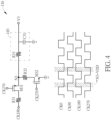
- FIG. 4 is a diagram illustrating the third detection circuit 116 according to one embodiment of the present invention.
- the third detection circuit 116 comprises transistors M31, M32, resistors R31, R32 and a low-pass filter 410, wherein the low-pass filter 410 comprises a resistor R33 and a capacitor C31.
- the transistor M31 is the P-type transistor while the transistor M32 is the N-type transistor, a gate electrode of the transistor M31 is coupled to the clock signal CK270, a first electrode of the M31 is coupled to a first electrode of the transistor M32 via the node N3 and the resistor R32, a second electrode of the transistor M31 is coupled to the clock signal CK180 via the resistor R31, and a second electrode of the transistor M32 is coupled to the ground voltage.
- the transistor M31 can be replaced by a switch with any different type, and this switch is controlled by the clock signal CK270 to selectively connect the clock signal CK180 to the node N3.
- the transistor M32 can be replaced by a switch with any different type, and this switch is controlled by the clock signal CK270 to selectively connect the node N3 to the ground voltage.
- the node N3 when the clock signal CK270 has a low voltage (e.g. ground voltage or 0V) and the clock signal CK180 has a high voltage such as a supply voltage VDD of the clock signal generator 130, the node N3 will have the high voltage (e.g. VDD); when both the clock signals CK270 and CK180 have the low voltage, the node N3 will have the low voltage; and when the clock signal CK270 has the high voltage, the node N3 will always have the low voltage because the transistor M32 with larger driving ability discharges the node N3.
- VDD supply voltage
- the third detection result V3 generated by filtering the voltage of the node N3 should be equal to (1/4) *VDD if the phase difference between the clock signals CK180 and CK270 is exactly equal to 90 degrees.
- the control circuit 120 may generate the control signal Vc to control the clock signal generator 130 to delay the phase of the clock signal CK270.
- the third detection result V3 is greater than (1/4)*VDD, it means that the phase difference between the clock signals CK180 and CK270 is greater than 90 degrees, and the control circuit 120 may generate the control signal Vc to control the clock signal generator 130 to advance the phase of the clock signal CK270.
- the third detection circuit 116 is configured to detect the phase difference based on rising edges of the clock signals CK180 and CK270.
- the transistor M31 may be implemented by the N-type transistor while the transistor M32 is implemented by the P-type transistor, for detecting the phase difference based on falling edges of the clock signals CK180 and CK270.
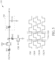
- FIG. 5 is a diagram illustrating the fourth detection circuit 118 according to one embodiment of the present invention.
- the fourth detection circuit 118 comprises transistors M41, M42, resistors R41, R42 and a low-pass filter 510, wherein the low-pass filter 510 comprises a resistor R43 and a capacitor C41.
- the transistor M41 is the P-type transistor while the transistor M42 is the N-type transistor, a gate electrode of the transistor M41 is coupled to the clock signal CK0, a first electrode of the M41 is coupled to a first electrode of the transistor M42 via the node N4 and the resistor R42, a second electrode of the transistor M41 is coupled to the clock signal CK270 via the resistor R41, and a second electrode of the transistor M42 is coupled to the ground voltage.
- the transistor M41 can be replaced by a switch with any different type, and this switch is controlled by the clock signal CK0 to selectively connect the clock signal CK270 to the node N4.
- the transistor M42 can be replaced by a switch with any different type, and this switch is controlled by the clock signal CK0 to selectively connect the node N4 to the ground voltage.
- the node N4 when the clock signal CK0 has a low voltage (e.g. ground voltage or 0V) and the clock signal CK270 has a high voltage such as a supply voltage VDD of the clock signal generator 130, the node N4 will have the high voltage (e.g. VDD) ; when both the clock signals CK0 and CK270 have the low voltage, the node N4 will have the low voltage; and when the clock signal CK0 has the high voltage, the node N4 will always have the low voltage because the transistor M42 with larger driving ability discharges the node N4.
- VDD supply voltage
- the fourth detection result V4 generated by filtering the voltage of the node N4 should be equal to (1/4) *VDD if the phase difference between the clock signals CK270 and CK0 is exactly equal to 90 degrees.
- the control circuit 120 may generate the control signal Vc to control the clock signal generator 130 to delay the phase of the clock signal CK0.
- the fourth detection result V4 is greater than (1/4)*VDD, it means that the phase difference between the clock signals CK270 and CK0 is greater than 90 degrees, and the control circuit 120 may generate the control signal Vc to control the clock signal generator 130 to advance the phase of the clock signal CK0.
- the fourth detection circuit 118 is configured to detect the phase difference based on rising edges of the clock signals CK270 and CK0.
- the transistor M41 may be implemented by the N-type transistor while the transistor M42 is implemented by the P-type transistor, for detecting the phase difference based on falling edges of the clock signals CK270 and CK180.
- the passive devices such as resistors R11, R21, R31 and R41 have small errors in process, phase detection mismatches of the first detection circuit 112, the second detection circuit 114, the third detection circuit 116 and the fourth detection circuit 118 can be improved.
- the node N1 may not exactly have the ground voltage or 0V when both the clock signals CK0 and CK90 have the low voltage due to large turn-on resistance of the transistor M11, causing the first detection result V1 has error.
- the first detection circuit 112 can be modified to have a compensation circuit to control the node N1 to have the ground voltage or 0V when both the clock signals CK0 and CK90 have the low voltage.
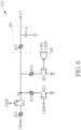
- the first detection circuit 112' further comprises the compensation circuit including a transistor M13, a resistor R14 and a NOR gate 610, wherein the NOR gate 610 receives the clock signals CK0 and CK90.
- the compensation circuit shown in FIG. 6 is for illustrative, not a limitation of the present invention. As long as the compensation circuit can discharge the node N1 when the transistor M11 is enabled and the clock signal CK0 has the low voltage (i.e., both the clock signals CK0 and CK90 have the low voltage), the compensation circuit can have any other suitable design. In one embodiment, the compensation circuit discharges the node N1 only when the transistor M11 is enabled and the clock signal CK0 has the low voltage.
- the compensation circuit is designed so that the node N1 is discharged when the clock signal CK0 has the low voltage and the clock signal CK90 have the high voltage.
- the node N2 may not exactly have the ground voltage or 0V when both the clock signals CK90 and CK180 have the low voltage due to large turn-on resistance of the transistor M21, causing the second detection result V2 has error.
- the second detection circuit 114 can be modified to have a compensation circuit to control the node N2 to have the ground voltage or 0V when both the clock signals CK90 and CK180 have the low voltage.
- the second detection circuit 114' further comprises the compensation circuit including a transistor M23, a resistor R24 and a NOR gate 710, wherein the NOR gate 710 receives the clock signals CK90 and CK180.
- the node N3 may not exactly have the ground voltage or 0V when both the clock signals CK180 and CK270 have the low voltage due to large turn-on resistance of the transistor M31, causing the second detection result V3 has error.
- the third detection circuit 116 can be modified to have a compensation circuit to control the node N3 to have the ground voltage or 0V when both the clock signals CK180 and CK270 have the low voltage.
- the third detection circuit 116' further comprises the compensation circuit including a transistor M33, a resistor R34 and a NOR gate 810, wherein the NOR gate 810 receives the clock signals CK180 and CK270.
- the node N4 may not exactly have the ground voltage or 0V when both the clock signals CK270 and CK0 have the low voltage due to large turn-on resistance of the transistor M41, causing the second detection result V4 has error.
- the third detection circuit 118 can be modified to have a compensation circuit to control the node N4 to have the ground voltage or 0V when both the clock signals CK270 and CK0 have the low voltage.
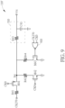
- the fourth detection circuit 118' further comprises the compensation circuit including a transistor M43, a resistor R44 and a NOR gate 910, wherein the NOR gate 910 receives the clock signals CK270 and CK0.
- the quadrature phase detector 110 may have the first detection circuit 112 only, or the quadrature phase detector 110 may have the first detection circuit 112 and the second detection circuit 114 only, or the quadrature phase detector 110 may have the first detection circuit 112, the second detection circuit 114 and the third detection circuit 116 only.
- the quadrature phase detector 110 may have the first detection circuit 112 and the second detection circuit 114 only, or the quadrature phase detector 110 may have the first detection circuit 112, the second detection circuit 114 and the third detection circuit 116 only.
- the present invention may also be defined by means of the following numbered clauses.
Landscapes
- Engineering & Computer Science (AREA)
- Power Engineering (AREA)
- Manipulation Of Pulses (AREA)
- Digital Transmission Methods That Use Modulated Carrier Waves (AREA)
Abstract
Description
- This application claims the benefit of
U.S. Provisional Application No. 63/255 ,030, filed on October 13th, 2021 . The content of the application is incorporated herein by reference. - A quadrature phase detector is usually provided to detect a phase difference between an in-phase clock signal and a quadrature clock signal, and a detection result of the quadrature phase detector may be used by a clock signal generator or a delay element to adjust the phase of the in-phase clock signal or the quadrature clock signal. The conventional quadrature phase detector is usually implemented by using active devices such as XOR gates, however, using XOR gates may increase the power consumption. In addition, if the quadrature phase detector is designed to detect four clock signals whose phases are 0 degree, 90 degrees, 180 degrees and 270 degrees, four sets of circuits are designed to detect the phase difference between clock signals with 0 degree and 90 degrees, the phase difference between clock signals with 90 degrees and 180 degrees, the phase difference between clock signals with 180 degrees and 270 degrees, and the phase difference between clock signals with 270 degrees and 0 degree. However, there may be mismatches between the four sets of circuits due to the semiconductor process, causing phase detection mismatches or phase detection errors.
- It is therefore an objective of the present invention to provide a quadrature phase detector in which most of the components are implemented by using passive components, to lower power consumption and improve the phase detection mismatches.
- According to one embodiment of the present invention, a quadrature phase detector comprising a detection circuit is disclosed. The detection circuit comprises a first switch, a second switch and a first filter, wherein the first switch is controlled by a second clock signal to selectively couple a first clock signal to a first node, the second switch is controlled by the second clock signal to selectively coupled the first node to a reference voltage, and the first filter is configured to filter voltages at the first node to generate a first detection result.
- According to one embodiment of the present invention, a circuitry comprising a clock signal generator, a detection circuit and a control circuit is disclosed. The clock signal generator is configured to generate a first clock signal and a second clock signal. The detection circuit comprises a first switch, a second switch and a first filter, wherein the first switch is controlled by a second clock signal to selectively couple a first clock signal to a first node, the second switch is controlled by the second clock signal to selectively coupled the first node to a reference voltage, and the first filter is configured to filter voltages at the first node to generate a first detection result. The control circuit is configured to generate a control signal to adjust a phase of the first clock signal or the second clock signal according to the first detection result.
- These and other objectives of the present invention will no doubt become obvious to those of ordinary skill in the art after reading the following detailed description of the preferred embodiment that is illustrated in the various figures and drawings.
-
-
FIG. 1 is a diagram illustrating a circuitry according to one embodiment of the present invention. -
FIG. 2 is a diagram illustrating the first detection circuit according to one embodiment of the present invention. -
FIG. 3 is a diagram illustrating the second detection circuit according to one embodiment of the present invention. -
FIG. 4 is a diagram illustrating the third detection circuit according to one embodiment of the present invention. -
FIG. 5 is a diagram illustrating the fourth detection circuit according to one embodiment of the present invention. -
FIG. 6 is a diagram illustrating the first detection circuit according to one embodiment of the present invention. -
FIG. 7 is a diagram illustrating the second detection circuit according to one embodiment of the present invention. -
FIG. 8 is a diagram illustrating the third detection circuit according to one embodiment of the present invention. -
FIG. 9 is a diagram illustrating the fourth detection circuit according to one embodiment of the present invention. - Certain terms are used throughout the following description and claims to refer to particular system components. As one skilled in the art will appreciate, manufacturers may refer to a component by different names. This document does not intend to distinguish between components that differ in name but not function. In the following discussion and in the claims, the terms "including" and "comprising" are used in an open-ended fashion, and thus should be interpreted to mean "including, but not limited to ...". The terms "couple" and "couples" are intended to mean either an indirect or a direct electrical connection. Thus, if a first device couples to a second device, that connection may be through a direct electrical connection, or through an indirect electrical connection via other devices and connections.
-
FIG. 1 is a diagram illustrating acircuitry 100 according to one embodiment of the present invention. As shown inFIG. 1 , thecircuitry 100 comprises aquadrature phase detector 110, acontrol circuit 120 and aclock signal generator 130, wherein thequadrature phase detector 110 comprises afirst detection circuit 112, asecond detection circuit 114, athird detection circuit 116 and afourth detection circuit 118. In this embodiment, thecircuitry 100 is configured to generate four clock signals CK0, CK90, CK180 and CK270 with ideal phases of 0 degree, 90 degrees, 180 degrees and 270 degrees, respectively. - In the operation of the
circuitry 100, thequadrature phase detector 110 is configured to detect phase differences between any two adjacent clock signals to generate detection results. Specifically, thefirst detection circuit 112 is configured to detect a phase difference between the clock signals CK0 and CK90 to generate a first detection result V1, thesecond detection circuit 114 is configured to detect a phase difference between the clock signals CK90 and CK180 to generate a second detection result V2, thethird detection circuit 116 is configured to detect a phase difference between the clock signals CK180 and CK270 to generate a third detection result V3, and thefourth detection circuit 118 is configured to detect a phase difference between the clock signals CK270 and CK0 to generate a fourth detection result V4. Then, thecontrol circuit 120 refers to the first detection result V1, the second detection result V2, the third detection result V3 and the fourth detection result V4 to determine if any one of the clock signals CK0 CK90, CK180 and CK270 needs to adjust the phase, and at least one control signal Vc is generated accordingly. Specifically, thecontrol circuit 120 can refer to the first detection result V1 to determine if the phase difference between the clock signals CK0 and CK90 is not equal to 90 degrees, and to generate the control signal Vc to theclock signal generator 130 to adjust the phase of the clock signal CK90. Thecontrol circuit 120 can refer to the second detection result V2 to determine if the phase difference between the clock signals CK90 and CK180 is not equal to 90 degrees, and to generate the control signal Vc to theclock signal generator 130 to adjust the phase of the clock signal CK180. Thecontrol circuit 120 can refer to the third detection result V3 to determine if the phase difference between the clock signals CK180 and CK270 is not equal to 90 degrees, and to generate the control signal Vc to theclock signal generator 130 to adjust the phase of the clock signal CK270. Thecontrol circuit 120 can refer to the fourth detection result V4 to determine if the phase difference between the clock signals CK270 and CK0 is not equal to 90 degrees, and to generate the control signal Vc to theclock signal generator 130 to adjust the phase of the clock signal CK0. - In this embodiment, at least a portion of the
first detection circuit 112, thesecond detection circuit 114 and thethird detection circuit 116 and thefourth detection circuit 118 are designed so that most of the components are implemented by using passive components, to lower power consumption and improve the phase detection mismatches. -
FIG. 2 is a diagram illustrating thefirst detection circuit 112 according to one embodiment of the present invention. As shown inFIG. 2 , thefirst detection circuit 112 comprises transistors M11, M12, resistors R11, R12 and a low-pass filter 210, wherein the low-pass filter 210 comprises a resistor R13 and a capacitor C11. In this embodiment, the transistor M11 is a P-type transistor while the transistor M12 is an N-type transistor, a gate electrode of the transistor M11 is coupled to the clock signal CK90, a first electrode of the M11 is coupled to a first electrode of the transistor M12 via the node N1 and the resistor R12, a second electrode of the transistor M11 is coupled to the clock signal CK0 via the resistor R11, and a second electrode of the transistor M12 is coupled to a ground voltage. - In another embodiment, the transistor M11 can be replaced by a switch with any different type, and this switch is controlled by the clock signal CK90 to selectively connect the clock signal CK0 to the node N1. In addition, the transistor M12 can be replaced by a switch with any different type, and this switch is controlled by the clock signal CK90 to selectively connect the node N1 to the ground voltage.
- In the operation of the
first detection circuit 112, when the clock signal CK90 has a low voltage (e.g. ground voltage or 0V) and the clock signal CK0 has a high voltage such as a supply voltage VDD of theclock signal generator 130, the node N1 will have the high voltage (e.g. VDD); when both the clock signals CK90 and CK0 have the low voltage, the node N1 will have the low voltage; and when the clock signal CK90 has the high voltage, the node N1 will always have the low voltage because the transistor M12 with larger driving ability discharges the node N1. Therefore, because the node N1 has the high voltage only during quarter-cycle of the clock signal CK0/CK90, the first detection result V1 generated by filtering the voltage of the node N1 should be equal to (1/4)*VDD if the phase difference between the clock signals CK0 and CK90 is exactly equal to 90 degrees. - In one embodiment, if the first detection result V1 is lower than (1/4)*VDD, it means that the phase difference between the clock signals CK0 and CK90 is less than 90 degrees, and the
control circuit 120 may generate the control signal Vc to control theclock signal generator 130 to delay the phase of the clock signal CK90. Similarly, if the first detection result V1 is greater than (1/4)*VDD, it means that the phase difference between the clock signals CK0 and CK90 is greater than 90 degrees, and thecontrol circuit 120 may generate the control signal Vc to control theclock signal generator 130 to advance the phase of the clock signal CK90. - In the embodiment shown in
FIG. 2 , thefirst detection circuit 112 is configured to detect the phase difference based on rising edges of the clock signals CK0 and CK90. In another embodiment, the transistor M11 may be implemented by an N-type transistor while the transistor M12 is implemented by the P-type transistor, for detecting the phase difference based on falling edges of the clock signals CK0 and CK90. -
FIG. 3 is a diagram illustrating thesecond detection circuit 114 according to one embodiment of the present invention. As shown inFIG. 3 , thesecond detection circuit 114 comprises transistors M21, M22, resistors R21, R22 and a low-pass filter 310, wherein the low-pass filter 310 comprises a resistor R23 and a capacitor C21. In this embodiment, the transistor M21 is a P-type transistor while the transistor M22 is an N-type transistor, a gate electrode of the transistor M21 is coupled to the clock signal CK180, a first electrode of the M21 is coupled to a first electrode of the transistor M22 via the node N2 and the resistor R22, a second electrode of the transistor M21 is coupled to the clock signal CK90 via the resistor R21, and a second electrode of the transistor M22 is coupled to the ground voltage. - In another embodiment, the transistor M21 can be replaced by a switch with any different type, and this switch is controlled by the clock signal CK180 to selectively connect the clock signal CK90 to the node N2. In addition, the transistor M22 can be replaced by a switch with any different type, and this switch is controlled by the clock signal CK180 to selectively connect the node N2 to the ground voltage.
- In the operation of the
second detection circuit 114, when the clock signal CK180 has a low voltage (e.g. ground voltage or 0V) and the clock signal CK90 has a high voltage such as a supply voltage VDD of theclock signal generator 130, the node N2 will have the high voltage (e.g. VDD); when both the clock signals CK180 and CK90 have the low voltage, the node N2 will have the low voltage; and when the clock signal CK180 has the high voltage, the node N2 will always have the low voltage because the transistor M22 with larger driving ability discharges the node N2. Therefore, because the node N2 has the high voltage only during quarter-cycle of the clock signal CK90/CK180, the second detection result V2 generated by filtering the voltage of the node N2 should be equal to (1/4) *VDD if the phase difference between the clock signals CK90 and CK180 is exactly equal to 90 degrees. - In one embodiment, if the second detection result V2 is lower than (1/4)*VDD, it means that the phase difference between the clock signals CK90 and CK180 is less than 90 degrees, and the
control circuit 120 may generate the control signal Vc to control theclock signal generator 130 to delay the phase of the clock signal CK180. Similarly, if the second detection result V2 is greater than (1/4)*VDD, it means that the phase difference between the clock signals CK90 and CK180 is greater than 90 degrees, and thecontrol circuit 120 may generate the control signal Vc to control theclock signal generator 130 to advance the phase of the clock signal CK180. - In the embodiment shown in
FIG. 3 , thesecond detection circuit 114 is configured to detect the phase difference based on rising edges of the clock signals CK90 and CK180. In another embodiment, the transistor M21 may be implemented by the N-type transistor while the transistor M22 is implemented by the P-type transistor, for detecting the phase difference based on falling edges of the clock signals CK90 and CK180. -
FIG. 4 is a diagram illustrating thethird detection circuit 116 according to one embodiment of the present invention. As shown inFIG. 4 , thethird detection circuit 116 comprises transistors M31, M32, resistors R31, R32 and a low-pass filter 410, wherein the low-pass filter 410 comprises a resistor R33 and a capacitor C31. In this embodiment, the transistor M31 is the P-type transistor while the transistor M32 is the N-type transistor, a gate electrode of the transistor M31 is coupled to the clock signal CK270, a first electrode of the M31 is coupled to a first electrode of the transistor M32 via the node N3 and the resistor R32, a second electrode of the transistor M31 is coupled to the clock signal CK180 via the resistor R31, and a second electrode of the transistor M32 is coupled to the ground voltage. - In another embodiment, the transistor M31 can be replaced by a switch with any different type, and this switch is controlled by the clock signal CK270 to selectively connect the clock signal CK180 to the node N3. In addition, the transistor M32 can be replaced by a switch with any different type, and this switch is controlled by the clock signal CK270 to selectively connect the node N3 to the ground voltage.
- In the operation of the
third detection circuit 116, when the clock signal CK270 has a low voltage (e.g. ground voltage or 0V) and the clock signal CK180 has a high voltage such as a supply voltage VDD of theclock signal generator 130, the node N3 will have the high voltage (e.g. VDD); when both the clock signals CK270 and CK180 have the low voltage, the node N3 will have the low voltage; and when the clock signal CK270 has the high voltage, the node N3 will always have the low voltage because the transistor M32 with larger driving ability discharges the node N3. Therefore, because the node N3 has the high voltage only during quarter-cycle of the clock signal CK180/CK270, the third detection result V3 generated by filtering the voltage of the node N3 should be equal to (1/4) *VDD if the phase difference between the clock signals CK180 and CK270 is exactly equal to 90 degrees. - In one embodiment, if the third detection result V3 is lower than (1/4)*VDD, it means that the phase difference between the clock signals CK180 and CK270 is less than 90 degrees, and the
control circuit 120 may generate the control signal Vc to control theclock signal generator 130 to delay the phase of the clock signal CK270. Similarly, if the third detection result V3 is greater than (1/4)*VDD, it means that the phase difference between the clock signals CK180 and CK270 is greater than 90 degrees, and thecontrol circuit 120 may generate the control signal Vc to control theclock signal generator 130 to advance the phase of the clock signal CK270. - In the embodiment shown in
FIG. 4 , thethird detection circuit 116 is configured to detect the phase difference based on rising edges of the clock signals CK180 and CK270. In another embodiment, the transistor M31 may be implemented by the N-type transistor while the transistor M32 is implemented by the P-type transistor, for detecting the phase difference based on falling edges of the clock signals CK180 and CK270. -
FIG. 5 is a diagram illustrating thefourth detection circuit 118 according to one embodiment of the present invention. As shown inFIG. 5 , thefourth detection circuit 118 comprises transistors M41, M42, resistors R41, R42 and a low-pass filter 510, wherein the low-pass filter 510 comprises a resistor R43 and a capacitor C41. In this embodiment, the transistor M41 is the P-type transistor while the transistor M42 is the N-type transistor, a gate electrode of the transistor M41 is coupled to the clock signal CK0, a first electrode of the M41 is coupled to a first electrode of the transistor M42 via the node N4 and the resistor R42, a second electrode of the transistor M41 is coupled to the clock signal CK270 via the resistor R41, and a second electrode of the transistor M42 is coupled to the ground voltage. - In another embodiment, the transistor M41 can be replaced by a switch with any different type, and this switch is controlled by the clock signal CK0 to selectively connect the clock signal CK270 to the node N4. In addition, the transistor M42 can be replaced by a switch with any different type, and this switch is controlled by the clock signal CK0 to selectively connect the node N4 to the ground voltage.
- In the operation of the
fourth detection circuit 118, when the clock signal CK0 has a low voltage (e.g. ground voltage or 0V) and the clock signal CK270 has a high voltage such as a supply voltage VDD of theclock signal generator 130, the node N4 will have the high voltage (e.g. VDD) ; when both the clock signals CK0 and CK270 have the low voltage, the node N4 will have the low voltage; and when the clock signal CK0 has the high voltage, the node N4 will always have the low voltage because the transistor M42 with larger driving ability discharges the node N4. Therefore, because the node N4 has the high voltage only during quarter-cycle of the clock signal CK270/CK0, the fourth detection result V4 generated by filtering the voltage of the node N4 should be equal to (1/4) *VDD if the phase difference between the clock signals CK270 and CK0 is exactly equal to 90 degrees. - In one embodiment, if the fourth detection result V4 is lower than (1/4)*VDD, it means that the phase difference between the clock signals CK270 and CK0 is less than 90 degrees, and the
control circuit 120 may generate the control signal Vc to control theclock signal generator 130 to delay the phase of the clock signal CK0.Similarly, if the fourth detection result V4 is greater than (1/4)*VDD, it means that the phase difference between the clock signals CK270 and CK0 is greater than 90 degrees, and thecontrol circuit 120 may generate the control signal Vc to control theclock signal generator 130 to advance the phase of the clock signal CK0. - In the embodiment shown in
FIG. 5 , thefourth detection circuit 118 is configured to detect the phase difference based on rising edges of the clock signals CK270 and CK0.In another embodiment, the transistor M41 may be implemented by the N-type transistor while the transistor M42 is implemented by the P-type transistor, for detecting the phase difference based on falling edges of the clock signals CK270 and CK180. - In the embodiment shown in
FIGs. 2-5 , because the components within thefirst detection circuit 112, thesecond detection circuit 114, thethird detection circuit 116 and thefourth detection circuit 118 do not need to be powered by the supply voltage VDD, power consumption of thecircuitry 100 can be greatly reduced. In addition, because the passive devices such as resistors R11, R21, R31 and R41 have small errors in process, phase detection mismatches of thefirst detection circuit 112, thesecond detection circuit 114, thethird detection circuit 116 and thefourth detection circuit 118 can be improved. - In the
first detection circuit 112 shown inFIG. 2 , the node N1 may not exactly have the ground voltage or 0V when both the clock signals CK0 and CK90 have the low voltage due to large turn-on resistance of the transistor M11, causing the first detection result V1 has error. To solve this problem, thefirst detection circuit 112 can be modified to have a compensation circuit to control the node N1 to have the ground voltage or 0V when both the clock signals CK0 and CK90 have the low voltage. Referring toFIG. 6 , the first detection circuit 112' further comprises the compensation circuit including a transistor M13, a resistor R14 and a NORgate 610, wherein the NORgate 610 receives the clock signals CK0 and CK90. In the operation of the compensation circuit shown inFIG. 6 , when both the clock signals CK0 and CK90 have the low voltage, an output signal of the NORgate 610 will enable the transistor M13 to discharge the node N1, so that the node N1 can have the ground voltage. Therefore, the first detection result V1 can reflect the phase difference of the clock signals CK0 and CK90 more accurately. - It is noted that the compensation circuit shown in
FIG. 6 is for illustrative, not a limitation of the present invention. As long as the compensation circuit can discharge the node N1 when the transistor M11 is enabled and the clock signal CK0 has the low voltage (i.e., both the clock signals CK0 and CK90 have the low voltage), the compensation circuit can have any other suitable design. In one embodiment, the compensation circuit discharges the node N1 only when the transistor M11 is enabled and the clock signal CK0 has the low voltage. - In addition, for the case that the transistor M11 is implemented by the N-type transistor, the compensation circuit is designed so that the node N1 is discharged when the clock signal CK0 has the low voltage and the clock signal CK90 have the high voltage.
- In the
second detection circuit 114 shown inFIG. 3 , the node N2 may not exactly have the ground voltage or 0V when both the clock signals CK90 and CK180 have the low voltage due to large turn-on resistance of the transistor M21, causing the second detection result V2 has error. To solve this problem, thesecond detection circuit 114 can be modified to have a compensation circuit to control the node N2 to have the ground voltage or 0V when both the clock signals CK90 and CK180 have the low voltage. Referring toFIG. 7 , the second detection circuit 114' further comprises the compensation circuit including a transistor M23, a resistor R24 and a NORgate 710, wherein the NORgate 710 receives the clock signals CK90 and CK180. In the operation of the compensation circuit shown inFIG. 7 , when both the clock signals CK90 and CK180 have the low voltage, an output signal of the NORgate 710 will enable the transistor M23 to discharge the node N2, so that the node N2 can have the ground voltage. Therefore, the second detection result V2 can reflect the phase difference of the clock signals CK90 and CK180 more accurately. - In the
third detection circuit 116 shown inFIG. 4 , the node N3 may not exactly have the ground voltage or 0V when both the clock signals CK180 and CK270 have the low voltage due to large turn-on resistance of the transistor M31, causing the second detection result V3 has error. To solve this problem, thethird detection circuit 116 can be modified to have a compensation circuit to control the node N3 to have the ground voltage or 0V when both the clock signals CK180 and CK270 have the low voltage. Referring toFIG. 8 , the third detection circuit 116' further comprises the compensation circuit including a transistor M33, a resistor R34 and a NORgate 810, wherein the NORgate 810 receives the clock signals CK180 and CK270. In the operation of the compensation circuit shown inFIG. 8 , when both the clock signals CK180 and CK270 have the low voltage, an output signal of the NORgate 810 will enable the transistor M33 to discharge the node N3, so that the node N3 can have the ground voltage. Therefore, the second detection result V3 can reflect the phase difference of the clock signals CK180 and CK270 more accurately. - In the
fourth detection circuit 118 shown inFIG. 5 , the node N4 may not exactly have the ground voltage or 0V when both the clock signals CK270 and CK0 have the low voltage due to large turn-on resistance of the transistor M41, causing the second detection result V4 has error. To solve this problem, thethird detection circuit 118 can be modified to have a compensation circuit to control the node N4 to have the ground voltage or 0V when both the clock signals CK270 and CK0 have the low voltage. Referring toFIG. 9 , the fourth detection circuit 118' further comprises the compensation circuit including a transistor M43, a resistor R44 and a NORgate 910, wherein the NORgate 910 receives the clock signals CK270 and CK0. In the operation of the compensation circuit shown inFIG. 9 , when both the clock signals CK270 and CK0 have the low voltage, an output signal of the NORgate 910 will enable the transistor M43 to discharge the node N4, so that the node N4 can have the ground voltage. Therefore, the second detection result V4 can reflect the phase difference of the clock signals CK270 and CK0 more accurately. - In the embodiment shown in
FIGs. 6-9 , because most of the components within the first detection circuit 112' , the second detection circuit 114' , the third detection circuit 116' and the fourth detection circuit 118' do not need to be powered by the supply voltage VDD, power consumption of thecircuitry 100 can be greatly reduced. In addition, because the passive devices such as resistors R11, R21, R31 and R41 have small errors in process, phase detection mismatches of the first detection circuit 112', the second detection circuit 114', the third detection circuit 116' and the fourth detection circuit 118' can be improved. - It is noted that quantity of the detection circuits within the
quadrature phase detector 110 is for illustrative, not a limitation of the present invention. In other embodiments, thequadrature phase detector 110 may have thefirst detection circuit 112 only, or thequadrature phase detector 110 may have thefirst detection circuit 112 and thesecond detection circuit 114 only, or thequadrature phase detector 110 may have thefirst detection circuit 112, thesecond detection circuit 114 and thethird detection circuit 116 only. These alternative designs should fall within the scope of the present invention. - Those skilled in the art will readily observe that numerous modifications and alterations of the device and method may be made while retaining the teachings of the invention. Accordingly, the above disclosure should be construed as limited only by the metes and bounds of the appended claims.
- The present invention may also be defined by means of the following numbered clauses.
- 1. A quadrature phase detector, comprising:
a first detection circuit, comprising:- a first switch, wherein the first switch is controlled by a second clock signal to selectively couple a first clock signal to a first node;
- a second switch, wherein the second switch is controlled by the second clock signal to selectively coupled the first node to a reference voltage; and
- a first filter, configured to filter voltages at the first node to generate a first detection result.
- 2. The quadrature phase detector of clause 1, wherein the first switch is a first transistor comprising a gate electrode, a first electrode and a second electrode, wherein the first transistor receives the first clock signal at the second electrode, and receives the second clock signal at the gate electrode; and the second switch is a second transistor comprising a gate electrode, a first electrode and a second electrode, wherein the first electrode of the second transistor is coupled to the first electrode of the first transistor at the first node, the second transistor receives the second clock signal at the gate electrode, and the second electrode of the second transistor is coupled to the reference voltage.
- 3. The quadrature phase detector of clause 2, wherein the first transistor is a P-type transistor, and the second transistor is an N-type transistor.
- 4. The quadrature phase detector of clause 2, wherein the first transistor is an N-type transistor, and the second transistor is a P-type transistor.
- 5. The quadrature phase detector of clause 1, wherein the first detection circuit further comprises:
a compensation circuit, configured to selectively provide a discharging path for discharging the first node. - 6. The quadrature phase detector of clause 5, wherein the compensation circuit is configured to provide the discharging path to discharge the first node when the first switch is enabled and the first clock signal has a low voltage level.
- 7. The quadrature phase detector of clause 1, wherein ideally a phase difference between the first clock signal and the second clock signal is equal to 90 degrees, and the quadrature phase detector further comprises:
a second detection circuit, comprising:- a third switch, wherein the third switch is controlled by a third clock signal to selectively couple the second clock signal to a second node;
- a fourth switch, wherein the fourth switch is controlled by the third clock signal to selectively coupled the second node to the reference voltage; and
- a second filter, configured to filter voltages at the second node to generate a second detection result.
- 8. The quadrature phase detector of clause 7, wherein the third switch is a third transistor comprising a gate electrode, a first electrode and a second electrode, wherein the third transistor receives the second clock signal at the second electrode, and receives a third clock signal at the gate electrode; and the fourth switch is a fourth transistor comprising a gate electrode, a first electrode and a second electrode, wherein the first electrode of the fourth transistor is coupled to the first electrode of the third transistor at the second node, the fourth transistor receives the third clock signal at the gate electrode, and the second electrode of the fourth transistor is coupled to the reference voltage.
- 9. The quadrature phase detector of clause 7, wherein ideally a phase difference between the second clock signal and the third clock signal is equal to 90 degrees, and the quadrature phase detector further comprises:
a third detection circuit, comprising:- a fifth switch, wherein the fifth switch is controlled by a fourth clock signal to selectively couple the third clock signal to a third node;
- a sixth switch, wherein the sixth switch is controlled by the fourth clock signal to selectively coupled the third node to the reference voltage; and
- a third filter, configured to filter voltages at the third node to generate a third detection result.
- 10. The quadrature phase detector of clause 9, wherein the fifth switch is a fifth transistor comprising a gate electrode, a first electrode and a second electrode, wherein the fifth transistor receives the third clock signal at the second electrode, and receives the fourth clock signal at the gate electrode; and the sixth switch is a sixth transistor comprising a gate electrode, a first electrode and a second electrode, wherein the first electrode of the sixth transistor is coupled to the first electrode of the fifth transistor at the third node, the sixth transistor receives the fourth clock signal at the gate electrode, and the second electrode of the sixth transistor is coupled to the reference voltage.
- 11.The quadrature phase detector of clause 9, wherein the first clock signal,
- the second clock signal, the third clock signal and the fourth clock signal are with phases 0 degree, 90 degrees, 180 degrees and 270 degrees, respectively, and the quadrature phase detector further comprises:
- a fourth detection circuit, comprising:
- a seventh switch, wherein the seventh switch is controlled by the first clock signal to selectively couple the fourth clock signal to a fourth node;
- an eighth switch, wherein the eighth switch is controlled by the first clock signal to selectively coupled the fourth node to the reference voltage; and
- a fourth filter, configured to filter voltages at the fourth node to generate a fourth detection result.
- 12. A circuitry, comprising:
- a clock signal generator, configured to generate a first clock signal and a second clock signal,
- a first detection circuit, comprising:
- a first switch, wherein the first switch is controlled by the second clock signal to selectively couple the first clock signal to a first node;
- a second switch, wherein the second switch is controlled by the second clock signal to selectively coupled the first node to a reference voltage; and
- a first filter, configured to filter voltages at the first node to generate a first detection result;
- a control circuit, coupled to the first detection circuit, configured to generate a control signal to adjust a phase of the first clock signal or the second clock signal according to the first detection result.
- 13. The circuitry of clause 12, wherein the first switch is a first transistor comprising a gate electrode, a first electrode and a second electrode, wherein the first transistor receives the first clock signal at the second electrode, and receives the second clock signal at the gate electrode; and the second switch is a second transistor comprising a gate electrode, a first electrode and a second electrode, wherein the first electrode of the second transistor is coupled to the first electrode of the first transistor at the first node, the second transistor receives the second clock signal at the gate electrode, and the second electrode of the second transistor is coupled to the reference voltage.
- 14. The circuitry of clause 13, wherein the first transistor is a P-type transistor, and the second transistor is an N-type transistor.
- 15. The circuitry of clause 13, wherein the first transistor is an N-type transistor, and the second transistor is a P-type transistor.
- 16. The circuitry of clause 12, wherein the first detection circuit further comprises:
a compensation circuit, configured to selectively provide a discharging path for discharging the first node. - 17. The circuitry of clause 16, wherein the compensation circuit is configured to provide the discharging path to discharge the first node when the first switch is enabled and the first clock signal has a low voltage level.
- 18. The circuitry of clause 12, wherein ideally a phase difference between the first clock signal and the second clock signal is equal to 90 degrees, and the quadrature phase detector further comprises:
a second detection circuit, comprising:- a third switch, wherein the third switch is controlled by a third clock signal to selectively couple the second clock signal to a second node;
- a fourth switch, wherein the fourth switch is controlled by the third clock signal to selectively coupled the second node to the reference voltage; and
- a second filter, configured to filter voltages at the second node to generate a second detection result.
- 19. The circuitry of clause 18, wherein ideally a phase difference between the second clock signal and the third clock signal is equal to 90 degrees, and the quadrature phase detector further comprises:
a third detection circuit, comprising:- a fifth switch, wherein the fifth switch is controlled by a fourth clock signal to selectively couple the third clock signal to a third node;
- a sixth switch, wherein the sixth switch is controlled by the fourth clock signal to selectively coupled the third node to the reference voltage; and
- a third filter, configured to filter voltages at the third node to generate a third detection result.
- 20. The circuitry of clause 19, wherein the first clock signal, the second clock signal, the third clock signal and the fourth clock signal are with phases 0 degree, 90 degrees, 180 degrees and 270 degrees, respectively, and the quadrature phase detector further comprises:
a fourth detection circuit, comprising:- a seventh switch, wherein the seventh switch is controlled by the first clock signal to selectively couple the fourth clock signal to a fourth node;
- an eighth switch, wherein the eighth switch is controlled by the first clock signal to selectively coupled the fourth node to the reference voltage; and
- a fourth filter, configured to filter voltages at the fourth node to generate a fourth detection result.
Claims (15)
- A quadrature phase detector (110), comprising:
a first detection circuit (112, 112'), comprising:a first switch, wherein the first switch is controlled by a second clock signal (CK90) to selectively couple a first clock signal (CK0) to a first node;a second switch, wherein the second switch is controlled by the second clock signal (CK90) to selectively coupled the first node to a reference voltage; anda first filter, configured to filter voltages at the first node to generate a first detection result. - The quadrature phase detector (110) of claim 1, wherein the first switch is a first transistor comprising a gate electrode, a first electrode and a second electrode, wherein the first transistor receives the first clock signal (CK0) at the second electrode, and receives the second clock signal (CK90) at the gate electrode; and the second switch is a second transistor comprising a gate electrode, a first electrode and a second electrode, wherein the first electrode of the second transistor is coupled to the first electrode of the first transistor at the first node, the second transistor receives the second clock signal (CK90) at the gate electrode, and the second electrode of the second transistor is coupled to the reference voltage.
- The quadrature phase detector (110) of claim 2, wherein the firsttransistor is a P-type transistor (M11), and the second transistor isan N-type transistor (M12);
or wherein the first transistor is an N-type transistor (M12), and the secondtransistor is a P-type transistor (M11). - The quadrature phase detector (110) of claim 1, wherein the first detection circuit (112, 112') further comprises:
a compensation circuit, configured to selectively provide a discharging path for discharging the first node. - The quadrature phase detector (110) of claim 4, wherein the compensation circuit is configured to provide the discharging path to discharge the first node when the first switch is enabled and the first clock signal (CK0) has a low voltage level.
- The quadrature phase detector (110) of claim 1, wherein ideally a phase difference between the first clock signal (CK0) and the second clock signal (CK90) is equal to 90 degrees, and the quadrature phase detector (110) further comprises:
a second detection circuit (114, 114'), comprising:a third switch, wherein the third switch is controlled by a third clock signal (CK180) to selectively couple the second clock signal (CK90) to a second node;a fourth switch, wherein the fourth switch is controlled by the third clock signal to selectively coupled the second node to the reference voltage; anda second filter, configured to filter voltages at the second node to generate a second detection result. - The quadrature phase detector (110) of claim 6, wherein ideally a phase difference between the second clock signal (CK90) and the third clock signal (CK180) is equal to 90 degrees, and the quadrature phase detector (110) further comprises:
a third detection circuit (116, 116'), comprising:a fifth switch, wherein the fifth switch is controlled by a fourth clock signal (CK270) to selectively couple the third clock signal (CK180) to a third node;a sixth switch, wherein the sixth switch is controlled by the fourth clock signal (CK270) to selectively coupled the third node to the reference voltage; anda third filter, configured to filter voltages at the third node to generate a third detection result. - A circuitry (100), comprising:a clock signal generator (130), configured to generate a first clock signal (CK0) and a second clock signal(CK90),a first detection circuit (112, 112'), comprising:a first switch, wherein the first switch is controlled by the second clock signal (CK90) to selectively couple the first clock signal (CK0) to a first node;a second switch, wherein the second switch is controlled by the second clock signal (CK90) to selectively coupled the first node to a reference voltage; anda first filter, configured to filter voltages at the first node to generate a first detection result;a control circuit (120), coupled to the first detection circuit (112, 112'), configured to generate a control signal to adjust a phase of the first clock signal (CK0) or the second clock signal (CK90) according to the first detection result.
- The circuitry (100) of claim 8, wherein the first switch is a first transistor comprising a gate electrode, a first electrode and a second electrode, wherein the first transistor receives the first clock signal (CK0) at the second electrode, and receives the second clock signal (CK90) at the gate electrode; and the second switch is a second transistor comprising a gate electrode, a first electrode and a second electrode, wherein the first electrode of the second transistor is coupled to the first electrode of the first transistor at the first node, the second transistor receives the second clock signal (CK90) at the gate electrode, and the second electrode of the second transistor is coupled to the reference voltage.
- The circuitry (100) of claim 9, wherein the first transistor is a P-typetransistor (M11), and the second transistor is an N-type transistor (M12);
or wherein the first transistor is an N-type transistor (M12), and the secondtransistor is a P-type transistor (M11). - The circuitry (100) of claim 8, wherein the first detection circuit (112, 112') further comprises:
a compensation circuit, configured to selectively provide a discharging path for discharging the first node. - The circuitry (100) of claim 11, wherein the compensation circuit is configured to provide the discharging path to discharge the first node when the first switch is enabled and the first clock signal (CK0) has a low voltage level.
- The circuitry (100) of claim 8, wherein ideally a phase difference between the first clock signal (CK0) and the second clock signal (CK90) is equal to 90 degrees, and the quadrature phase detector (110) further comprises:
a second detection circuit (114, 114'), comprising:a third switch, wherein the third switch is controlled by a third clock signal (CK180) to selectively couple the second clock signal (CK90) to a second node;a fourth switch, wherein the fourth switch is controlled by the third clock signal (CK180) to selectively coupled the second node to the reference voltage; anda second filter, configured to filter voltages at the second node to generate a second detection result. - The circuitry (100) of claim 13, wherein ideally a phase difference between the second clock signal (CK90) and the third clock signal (CK180) is equal to 90 degrees, and the quadrature phase detector (110) further comprises:
a third detection circuit (116, 116'), comprising:a fifth switch, wherein the fifth switch is controlled by a fourth clock signal (CK270) to selectively couple the third clock signal (CK180) to a third node;a sixth switch, wherein the sixth switch is controlled by the fourth
clock signal (CK270) to selectively coupled the third node to the reference voltage; anda third filter, configured to filter voltages at the third node to generate a third detection result. - The circuitry (100) of claim 14, wherein the first clock signal(CK0), the second clock signal (CK90), the third clock signal (CK180) and the fourth clock signal (CK270) are with phases 0 degree, 90 degrees, 180 degrees and 270 degrees, respectively, and the quadrature phase detector (110) further comprises:
a fourth detection circuit (118, 118'), comprising:a seventh switch, wherein the seventh switch is controlled by the first clock signal (CK0) to selectively couple the fourth clock signal (CK270) to a fourth node;an eighth switch, wherein the eighth switch is controlled by the first clock signal (CK0) to selectively coupled the fourth node to the reference voltage; anda fourth filter, configured to filter voltages at the fourth node to generate a fourth detection result.
Applications Claiming Priority (2)
| Application Number | Priority Date | Filing Date | Title |
|---|---|---|---|
| US202163255030P | 2021-10-13 | 2021-10-13 | |
| US17/857,161 US12212325B2 (en) | 2021-10-13 | 2022-07-04 | Low power quadrature phase detector |
Publications (1)
| Publication Number | Publication Date |
|---|---|
| EP4167487A1 true EP4167487A1 (en) | 2023-04-19 |
Family
ID=83005881
Family Applications (1)
| Application Number | Title | Priority Date | Filing Date |
|---|---|---|---|
| EP22186206.3A Pending EP4167487A1 (en) | 2021-10-13 | 2022-07-21 | Low power quadrature phase detector |
Country Status (4)
| Country | Link |
|---|---|
| US (1) | US12212325B2 (en) |
| EP (1) | EP4167487A1 (en) |
| CN (1) | CN115967378A (en) |
| TW (1) | TWI858381B (en) |
Citations (2)
| Publication number | Priority date | Publication date | Assignee | Title |
|---|---|---|---|---|
| US20170222796A1 (en) * | 2016-02-01 | 2017-08-03 | Oracle International Corporation | Phased clock error handling |
| US20200186323A1 (en) * | 2018-12-05 | 2020-06-11 | Samsung Electronics Co., Ltd. | System and method for providing fast-settling quadrature detection and correction |
Family Cites Families (7)
| Publication number | Priority date | Publication date | Assignee | Title |
|---|---|---|---|---|
| US4682047A (en) * | 1985-08-29 | 1987-07-21 | Siemens Aktiengesellschaft | Complementary metal-oxide-semiconductor input circuit |
| JP3770741B2 (en) * | 1998-11-20 | 2006-04-26 | 富士通株式会社 | Semiconductor integrated circuit and method for switching source potential of transistor in semiconductor integrated circuit |
| KR101036922B1 (en) * | 2008-04-11 | 2011-05-25 | 주식회사 하이닉스반도체 | Quadrature phase correction circuit |
| TWI532325B (en) | 2011-01-04 | 2016-05-01 | 智原科技股份有限公司 | Phase detector, phase detecting method, and clock-and-data recovery device |
| CN108009112A (en) * | 2017-09-27 | 2018-05-08 | 上海玮舟微电子科技有限公司 | A kind of high-frequency clock IQ phase calibration circuit |
| KR102279606B1 (en) | 2017-10-26 | 2021-07-21 | 에스케이하이닉스 주식회사 | Duty cycle detector and phase differnece detector |
| US11632098B2 (en) * | 2021-03-24 | 2023-04-18 | Qualcomm Incorporated | Polyphase filter with interphase coupling |
-
2022
- 2022-07-04 US US17/857,161 patent/US12212325B2/en active Active
- 2022-07-21 EP EP22186206.3A patent/EP4167487A1/en active Pending
- 2022-08-24 TW TW111131905A patent/TWI858381B/en active
- 2022-08-25 CN CN202211028023.4A patent/CN115967378A/en active Pending
Patent Citations (2)
| Publication number | Priority date | Publication date | Assignee | Title |
|---|---|---|---|---|
| US20170222796A1 (en) * | 2016-02-01 | 2017-08-03 | Oracle International Corporation | Phased clock error handling |
| US20200186323A1 (en) * | 2018-12-05 | 2020-06-11 | Samsung Electronics Co., Ltd. | System and method for providing fast-settling quadrature detection and correction |
Non-Patent Citations (2)
| Title |
|---|
| ANONYMOUS: "Pass transistor logic - Wikipedia", 29 March 2021 (2021-03-29), pages 1 - 4, XP093009148, Retrieved from the Internet <URL:https://en.wikipedia.org/w/index.php?title=Pass_transistor_logic&oldid=1014867294> [retrieved on 20221217] * |
| FAIROOZ SHAIK ET AL: "Revisiting the Utility of Transmission Gate and Passtransistor Logic Styles in CMOS VLSI Design", 2021 3RD INTERNATIONAL CONFERENCE ON SIGNAL PROCESSING AND COMMUNICATION (ICPSC), IEEE, 13 May 2021 (2021-05-13), pages 276 - 280, XP033924761, [retrieved on 20210609], DOI: 10.1109/ICSPC51351.2021.9451645 * |
Also Published As
| Publication number | Publication date |
|---|---|
| CN115967378A (en) | 2023-04-14 |
| US20230113143A1 (en) | 2023-04-13 |
| TW202316786A (en) | 2023-04-16 |
| TWI858381B (en) | 2024-10-11 |
| US12212325B2 (en) | 2025-01-28 |
Similar Documents
| Publication | Publication Date | Title |
|---|---|---|
| JP5960228B2 (en) | RF buffer circuit having dynamic bias | |
| US7750703B2 (en) | Duty cycle correcting circuit | |
| CN101702575B (en) | Logic control interface circuit applied to negative voltage charge pump | |
| US7212027B2 (en) | Disconnection and short detecting circuit that can detect disconnection and short of a signal line transmitting a differential clock signal | |
| US7710177B2 (en) | Latch device having low-power data retention | |
| CN103346784A (en) | Matching type charge pump circuit for phase-locked loop | |
| US7274227B2 (en) | Power-on reset circuit | |
| CN101566658A (en) | Transient detection circuit | |
| US8736311B2 (en) | Semiconductor integrated circuit | |
| WO2021163422A1 (en) | Data bus signal conditioner and level shifter | |
| CN111934657B (en) | Low-power-consumption power-on reset and power-off reset circuit | |
| EP4167488A1 (en) | Poly phase filter with phase error enhance technique | |
| CN116073801B (en) | Phase interpolator and phase buffer circuits | |
| US7187218B2 (en) | Reset generator circuit for generating a reset signal | |
| US7772853B2 (en) | Semiconductor device | |
| US12212325B2 (en) | Low power quadrature phase detector | |
| US20230231551A1 (en) | High bandwidth and low power transmitter | |
| CN112994671B (en) | Low-power-consumption small-area high-precision power-on reset circuit | |
| KR20100010497A (en) | Oscillation detecting circuit | |
| EP4315606A1 (en) | Novel delay cell for quadrature clock generation with insensitivity to pvt variation and equal rising/falling edges | |
| CN119765220B (en) | Short-circuit protection circuit adapting to bus voltage and high-voltage integrated circuit thereof | |
| US6556092B1 (en) | Low consumption oscillator | |
| US6636082B1 (en) | System and method for detecting a negative supply fault | |
| TWI516893B (en) | Voltage clamper | |
| CN118539914A (en) | Level shift circuit, chip and electronic equipment |
Legal Events
| Date | Code | Title | Description |
|---|---|---|---|
| PUAI | Public reference made under article 153(3) epc to a published international application that has entered the european phase |
Free format text: ORIGINAL CODE: 0009012 |
|
| STAA | Information on the status of an ep patent application or granted ep patent |
Free format text: STATUS: THE APPLICATION HAS BEEN PUBLISHED |
|
| AK | Designated contracting states |
Kind code of ref document: A1 Designated state(s): AL AT BE BG CH CY CZ DE DK EE ES FI FR GB GR HR HU IE IS IT LI LT LU LV MC MK MT NL NO PL PT RO RS SE SI SK SM TR |
|
| P01 | Opt-out of the competence of the unified patent court (upc) registered |
Effective date: 20230607 |
|
| STAA | Information on the status of an ep patent application or granted ep patent |
Free format text: STATUS: REQUEST FOR EXAMINATION WAS MADE |
|
| 17P | Request for examination filed |
Effective date: 20231006 |
|
| RBV | Designated contracting states (corrected) |
Designated state(s): AL AT BE BG CH CY CZ DE DK EE ES FI FR GB GR HR HU IE IS IT LI LT LU LV MC MK MT NL NO PL PT RO RS SE SI SK SM TR |