EP4167405A1 - Laser diode element and method for manufacturing same - Google Patents
Laser diode element and method for manufacturing same Download PDFInfo
- Publication number
- EP4167405A1 EP4167405A1 EP21822276.8A EP21822276A EP4167405A1 EP 4167405 A1 EP4167405 A1 EP 4167405A1 EP 21822276 A EP21822276 A EP 21822276A EP 4167405 A1 EP4167405 A1 EP 4167405A1
- Authority
- EP
- European Patent Office
- Prior art keywords
- protrusion
- laser diode
- outer portion
- region
- diode element
- Prior art date
- Legal status (The legal status is an assumption and is not a legal conclusion. Google has not performed a legal analysis and makes no representation as to the accuracy of the status listed.)
- Pending
Links
Images








Classifications
-
- H—ELECTRICITY
- H01—ELECTRIC ELEMENTS
- H01S—DEVICES USING THE PROCESS OF LIGHT AMPLIFICATION BY STIMULATED EMISSION OF RADIATION [LASER] TO AMPLIFY OR GENERATE LIGHT; DEVICES USING STIMULATED EMISSION OF ELECTROMAGNETIC RADIATION IN WAVE RANGES OTHER THAN OPTICAL
- H01S5/00—Semiconductor lasers
- H01S5/02—Structural details or components not essential to laser action
- H01S5/0201—Separation of the wafer into individual elements, e.g. by dicing, cleaving, etching or directly during growth
- H01S5/0202—Cleaving
-
- H—ELECTRICITY
- H01—ELECTRIC ELEMENTS
- H01S—DEVICES USING THE PROCESS OF LIGHT AMPLIFICATION BY STIMULATED EMISSION OF RADIATION [LASER] TO AMPLIFY OR GENERATE LIGHT; DEVICES USING STIMULATED EMISSION OF ELECTROMAGNETIC RADIATION IN WAVE RANGES OTHER THAN OPTICAL
- H01S5/00—Semiconductor lasers
- H01S5/20—Structure or shape of the semiconductor body to guide the optical wave ; Confining structures perpendicular to the optical axis, e.g. index or gain guiding, stripe geometry, broad area lasers, gain tailoring, transverse or lateral reflectors, special cladding structures, MQW barrier reflection layers
- H01S5/22—Structure or shape of the semiconductor body to guide the optical wave ; Confining structures perpendicular to the optical axis, e.g. index or gain guiding, stripe geometry, broad area lasers, gain tailoring, transverse or lateral reflectors, special cladding structures, MQW barrier reflection layers having a ridge or stripe structure
-
- H—ELECTRICITY
- H01—ELECTRIC ELEMENTS
- H01S—DEVICES USING THE PROCESS OF LIGHT AMPLIFICATION BY STIMULATED EMISSION OF RADIATION [LASER] TO AMPLIFY OR GENERATE LIGHT; DEVICES USING STIMULATED EMISSION OF ELECTROMAGNETIC RADIATION IN WAVE RANGES OTHER THAN OPTICAL
- H01S5/00—Semiconductor lasers
- H01S5/40—Arrangement of two or more semiconductor lasers, not provided for in groups H01S5/02 - H01S5/30
- H01S5/4025—Array arrangements, e.g. constituted by discrete laser diodes or laser bar
- H01S5/4031—Edge-emitting structures
-
- H—ELECTRICITY
- H01—ELECTRIC ELEMENTS
- H01S—DEVICES USING THE PROCESS OF LIGHT AMPLIFICATION BY STIMULATED EMISSION OF RADIATION [LASER] TO AMPLIFY OR GENERATE LIGHT; DEVICES USING STIMULATED EMISSION OF ELECTROMAGNETIC RADIATION IN WAVE RANGES OTHER THAN OPTICAL
- H01S5/00—Semiconductor lasers
- H01S5/02—Structural details or components not essential to laser action
- H01S5/022—Mountings; Housings
- H01S5/0233—Mounting configuration of laser chips
- H01S5/0234—Up-side down mountings, e.g. Flip-chip, epi-side down mountings or junction down mountings
-
- H—ELECTRICITY
- H01—ELECTRIC ELEMENTS
- H01S—DEVICES USING THE PROCESS OF LIGHT AMPLIFICATION BY STIMULATED EMISSION OF RADIATION [LASER] TO AMPLIFY OR GENERATE LIGHT; DEVICES USING STIMULATED EMISSION OF ELECTROMAGNETIC RADIATION IN WAVE RANGES OTHER THAN OPTICAL
- H01S5/00—Semiconductor lasers
- H01S5/04—Processes or apparatus for excitation, e.g. pumping, e.g. by electron beams
- H01S5/042—Electrical excitation ; Circuits therefor
- H01S5/0425—Electrodes, e.g. characterised by the structure
- H01S5/04256—Electrodes, e.g. characterised by the structure characterised by the configuration
-
- H—ELECTRICITY
- H01—ELECTRIC ELEMENTS
- H01S—DEVICES USING THE PROCESS OF LIGHT AMPLIFICATION BY STIMULATED EMISSION OF RADIATION [LASER] TO AMPLIFY OR GENERATE LIGHT; DEVICES USING STIMULATED EMISSION OF ELECTROMAGNETIC RADIATION IN WAVE RANGES OTHER THAN OPTICAL
- H01S5/00—Semiconductor lasers
- H01S5/30—Structure or shape of the active region; Materials used for the active region
- H01S5/34—Structure or shape of the active region; Materials used for the active region comprising quantum well or superlattice structures, e.g. single quantum well [SQW] lasers, multiple quantum well [MQW] lasers or graded index separate confinement heterostructure [GRINSCH] lasers
- H01S5/343—Structure or shape of the active region; Materials used for the active region comprising quantum well or superlattice structures, e.g. single quantum well [SQW] lasers, multiple quantum well [MQW] lasers or graded index separate confinement heterostructure [GRINSCH] lasers in AIIIBV compounds, e.g. AlGaAs-laser, InP-based laser
- H01S5/34333—Structure or shape of the active region; Materials used for the active region comprising quantum well or superlattice structures, e.g. single quantum well [SQW] lasers, multiple quantum well [MQW] lasers or graded index separate confinement heterostructure [GRINSCH] lasers in AIIIBV compounds, e.g. AlGaAs-laser, InP-based laser with a well layer based on Ga(In)N or Ga(In)P, e.g. blue laser
Definitions
- the present invention relates to a laser diode element and a method for manufacturing the same.
- Patent Literature 1 describes an optically integrated semiconductor light emitting device having a plurality of light emitting device structures on a nitride semiconductor substrate.
- the shape of the light emitting device structures is in line symmetry with respect to the center line of the semiconductor light emitting device.
- Patent Literature 1 describes a GaN substrate as an example of a nitride semiconductor substrate, and indicates that the end face of the semiconductor light emitting device is formed by cleaving the GaN substrate.
- Patent Literature 1 Japanese Unexamined Patent Application Publication No. 2006-216772
- the shape of the end face formed by cleavage sometimes varies with the shape of the stacked body including the nitride semiconductor substrate.
- the present disclosure includes the following invention.
- a method for manufacturing a laser diode element including:
- a laser diode element including:
- FIG. 1 is a flowchart showing the method for manufacturing a laser diode element according to an embodiment of the present invention.
- the method for manufacturing a laser diode element of the present embodiment includes a stacked body preparation step S101, a cleavage step S 102, and a Dividing step S103.
- FIG. 2 to FIG. 12B are schematic views showing the method for manufacturing a laser diode element according to an embodiment of the present invention.
- a stacked body 100 is prepared.
- the stacked body 100 shown in FIG. 2 is a wafer.
- the stacked body 100 includes a plurality of element regions 400 that are defined in top view by a plurality of planned cleavage lines 200 and a plurality of planned division lines 300 intersecting the planned cleavage lines 200.
- the lines extending to the left and right in the drawing are the planned cleavage lines 200
- the lines extending in the vertical direction in the drawing are the planned division lines 300.
- the planned cleavage lines 200 and the planned division lines 300 are both virtual lines.
- the planned cleavage lines 200 and the planned division lines 300 intersect at a right angle, for example.
- the element regions 400 are rectangles, for example.
- the ends of all the planned cleavage lines 200 and the planned division lines 300 are aligned with the outer edge of the stacked body 100, when the planned cleavage lines 200 and/or the planned division lines 300 may be absent in portions that do not complete a laser diode element.
- the stacked body 100 may be a wafer as shown in FIG. 2 , or may be a divided piece obtained by dividing the wafer into a plurality of pieces.
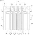
- FIG. 3 is a schematic top view of a stacked body showing a partial enlarged portion of the stacked body.
- the pattern as shown in FIG. 3 is disposed in each of the element regions 400.
- all of the element regions 400 have the same pattern. Some of the element regions 400 may, however, have a different pattern.
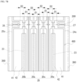
- FIG. 4A is a partial enlarged view of FIG. 3 ;
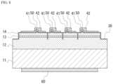
- FIG. 4B is a cross-sectional view along the line IVB-IVB of FIG. 4A ;
- FIG. 4C is a cross-sectional view along the line IVC-IVC of FIG. 4A .
- the line IVB-IVB in FIG. 4A coincides with a planned cleavage line 200. That is, FIG. 4B is a cross-sectional view along a planned cleavage line 200.
- the stacked body 100 includes a nitride semiconductor substrate 11, a first conductivity type semiconductor layer 12, an active layer 13, and a second conductivity type semiconductor layer 14.
- the first conductivity type semiconductor layer 12 is provided on the nitride semiconductor substrate 11.
- the active layer 13 is provided on the first conductivity type semiconductor layer 12.
- the second conductivity type semiconductor layer 14 is provided on the active layer 13.
- a GaN substrate is prepared as the nitride semiconductor substrate 11.
- the readily cleavable plane of a nitride semiconductor having a Wurtzite structure, such as GaN and the like, is the m-plane (that is, the ⁇ 10-10 ⁇ plane).
- the planned cleavage lines 200 preferably coincide with the m-plane in top view. Consequently, cleavage can be performed very precisely along the planned cleavage lines 200.
- the expression "coincide with the m-plane” is not limited to the case of exactly coinciding with the m-plane, and also includes a case in which the angle with respect to m-plane is 0.1 degree or less.
- the upper surface of the nitride semiconductor substrate 11 may be the c-plane (that is, the (0001) plane or the (000-1) plane), and the planned cleavage lines 200 are made to coincide with the m-plane.
- the c-plane is not limited to a plane that exactly coincides with the (0001) plane or the (000-1) plane, and also includes planes having an off angle within the range of ⁇ 0.03 to 1 degree.
- the shape of the nitride semiconductor substrate 11 is circular in top view, for example.
- a substrate having an orientation flat (OF) may be used as the nitride semiconductor substrate 11. If the nitride semiconductor substrate 11 is a substrate having an OF, the planned cleavage lines 200 can be aligned with the m-plane by using the OF as a reference.
- OF orientation flat
- the semiconductor constituting the first conductivity type semiconductor layer 12, the active layer 13, and the second conductivity type semiconductor layer 14 can be a nitride semiconductor, an example being a group III nitride semiconductor.
- group III nitride semiconductors include GaN, InGaN, and AlGaN.
- the first conductivity type semiconductor layer 12 is an n-type semiconductor layer, for example.
- the second conductivity type semiconductor layer 14 is a p-type semiconductor layer, for example.
- the nitride semiconductor substrate 11, the first conductivity type semiconductor layer 12, the active layer 13, and the second conductivity type semiconductor layer 14 may be in direct contact with each other, or another semiconductor layer may be disposed in between them.
- an undoped layer may be disposed between the second conductivity type semiconductor layer 14 and the active layer 13.
- the active layer 13 can have a multiple quantum well structure or a single quantum well structure.
- Examples of the plurality of semiconductor layers formed on the nitride semiconductor substrate 11 include an n-side clad layer, an n-side optical guide layer, the active layer 13, a p-side electron confinement layer, a p-side optical guide layer, a p-side clad layer, and a p-side contact layer, in that order starting from the nitride semiconductor substrate 11 side.
- the n-side clad layer is the first conductivity type semiconductor layer 12, and the p-side clad layer is the second conductivity type semiconductor layer 14.
- the plurality of semiconductor layers including the first conductivity type semiconductor layer 12, the active layer 13, and the second conductivity type semiconductor layer 14 can be formed, for example, by metal organic chemical vapor deposition (MOCVD).
- Each of the plurality of element regions 400 includes a plurality of protrusions 20.
- the number of protrusions 20 included in a single element region 400 is two or more, and may be three or more.
- the protrusions 20 in one element region 400 will include a first protrusion 20a, a second protrusion 20b, and one or more intermediate protrusions 20c.
- the first protrusion 20a is located on the side where the cleavage begins.
- the second protrusion 20b is located on the side where the cleavage ends.
- FIG. 4A to FIR. 4C the right side in the drawing is the side where the cleavage begins, and the left side in the drawing is the side where the cleavage ends.
- the intermediate protrusions 20c are located between the first protrusion 20a and the second protrusion 20b.
- the number of intermediate protrusions is two, for example.
- the protrusions 20 each have a first side surface 21, a second side surface 22, and a ridge 23.
- the first side surface 21 and the second side surface 22 are surfaces connecting the two planned cleavage lines 200 that definition a single element region 400.
- the first side surface 21 and the second side surface 22 are connected to each other via two planned cleavage lines 200.
- the outer edge of one protrusion 20 is constituted by two planned cleavage lines 200, the first side surface 21, and the second side surface 22.
- the first side surface 21 and the second side surface 22 may be inclined with respect to the upper surface of the protrusion 20, in which case the outer edge of the protrusion 20 can be defined using the upper end of the first side surface 21 and the upper end of the second side surface 22.
- the side surface on the right side in the drawing is the first side surface 21, and the side surface on the left side in the drawing is the second side surface 22.
- the ridges 23 are disposed between the first side surface 21 and the second side surface 22 in top view.
- the lengthwise direction of the ridges 23 is a direction that intersects the planned cleavage lines 200. That is, the ridges 23 have a long shape, and their lengthwise direction is a direction that intersects the planned cleavage lines 200.
- the lengthwise direction of the ridges 23 may be parallel to the planned division lines 300.
- the ridges 23 are in the form of stripes, for example.
- An optical waveguide can be defined by the ridges 23.
- the portion of the active layer 13 directly below the ridges 23 and the peripheral portion thereof can be an optical waveguide.
- the laser diode element thus obtained has a plurality of optical waveguides.
- the ridges 23 are formed one for each protrusion 20, for example. Consequently, in the laser diode element thus obtained, drive control of the plurality of optical waveguides can be carried out independently.
- the ridges 23 are formed, for example, on part of the upper surface of the second conductivity type semiconductor layer 14.
- the protrusions 20 including the ridges 23 can be formed by removing a part of the semiconductor layers on the nitride semiconductor substrate 11 by using photolithography and etching, for example.
- the lower end of the first side surface 21 and the lower end of the second side surface 22 are located below the lower surface of the active layer 13. Consequently, since the active layer 13 of the plurality of protrusions 20 is divided, in the resulting laser diode element each of the plurality of optical waveguides corresponding to the protrusions 20 can be driven individually. Also, since the lower end of the first side surface 21 is located below the lower surface of the active layer 13, the end face constituting a part of the optical waveguide is formed by cleavage starting from the first side surface 21 in the cleavage step (discussed below). Therefore, the shape of the protrusion 20 can affect the shape of the end face constituting a part of the optical waveguide.
- the lower end of the first side surface 21 and the lower end of the second side surface 22 are located, for example, in the first conductivity type semiconductor layer 12.
- the upper end of the first side surface 21 and the upper end of the second side surface 22 are located, for example, in the second conductivity type semiconductor layer 14.
- the second conductivity type semiconductor layer 14 is disposed on each of the plurality of protrusions 20.
- the second conductivity type semiconductor layer 14 on one protrusion 20 and the second conductivity type semiconductor layer 14 on another protrusion 20 are not linked and are separated from each other.
- one element region 400 can be said to include a plurality of second conductivity type semiconductor layers 14.
- the distance between the first protrusion 20a and the planned division line 300 can be made shorter than the distance between the second protrusion 20b and the planned division line 300 on the planned cleavage line 200.
- This asymmetry in distance can be used to distinguish between the portion on the light emitting side and the portion on the light reflecting side. Also, this asymmetry in distance can be used to distinguish between the end face on the light emitting side and the end face on the light reflecting side in the laser diode element after separation into individual pieces.
- FIG. 5A and FIG. 5B are schematic top views illustrating the shape of the protrusions.
- FIG. 5A is a view showing only the protrusions 20, the ridges 23, the planned cleavage lines 200, and the planned division lines 300 in the same region as FIG. 3 , and FIG. 5B showing these in the same region as FIG. 4A .
- the protrusions 20 are indicated by solid lines, and the ridges 23 are indicated by broken lines.
- a first distance D1 from the first side surface 21 to the ridge 23 on a planned cleavage line 200 is different from a second distance D2 from the second side surface 22 to the ridge 23 on a planned cleavage line 200 in top view.
- the plurality of first distances D1 in one element region 400 are all equal.
- the distance from the start of cleavage in each protrusion 20 to the portion corresponding to the optical waveguide can be made more uniform in the cleavage step discussed below. It is believed that this makes it possible for the shape of the end face formed in the cleavage step (discussed below) to be made more uniform in the portion corresponding to the optical waveguide of each protrusion 20. As a result, variation in the characteristics of the plurality of laser beams corresponding to the plurality of ridges of the obtained laser diode element can be reduced. Also, variation between the laser diode elements can be reduced. It should be noted that the phrase "the first distances D1 are equal" not only means that the first distances D1 are exactly the same, and also encompasses a difference of 1 ⁇ m or less between the smallest first distance D1 and the largest first distance D1.
- the second distance D2 is the distance from the ridge 23 to the second side surface 22 in the cleavage direction, the influence that the portion corresponding to the optical waveguide has on cleavage is believed to be less than that of the first distance D1. Therefore, the plurality of second distances D2 in a single element region 400 need not be equal. In FIG. 5B , the second distances D2 are all equal. Making all of the second distances D2 equal is believed to make it possible for the shape of the end face formed in the cleavage step to be more uniform.
- the first distance D1 is preferably 20 ⁇ m or more.
- the above-mentioned effect of having all the first distances D1 be the same is more easily obtained the closer the first side surface 21 and the ridge 23 are together. Therefore, the first distance D1 is preferably less than 80 ⁇ m, and more preferably 50 ⁇ m or less. Also, the first distance D1 is preferably greater than the second distance D2.
- the second distance D2 can be 5 ⁇ m or more.
- the second distance D2 can be less than 50 ⁇ m, and is preferably less than 20 ⁇ m. This makes it possible for the laser diode element to be made more compact.
- the width of the protrusion 20 in the direction along the planned cleavage line 200 can be 20 ⁇ m or more, for example.
- the shortest distance between two adjacent protrusions 20 in one element region 400 can be 1 ⁇ m or more, for example, and is preferably 2 ⁇ m or more. This reduces the possibility of short-circuiting between adjacent protrusions 20.
- the distance between protrusions 20 refers to the distance between the outer edge of one protrusion 20 and the outer edge of the other protrusion 20 in top view.
- the width of a protrusion 20 in the direction running along the planned cleavage line 200 can be 150 ⁇ m or less, and can be 50 ⁇ m or less. This makes it possible for the laser diode element to be more compact.
- a protrusion 20 has a first region located on the side of the first side surface 21, and a second region located on the side of the second side surface 22, with a ridge 23 serving as a boundary.
- the protrusion 20 may have an outer portion and an inner portion having different widths in the direction running along the planned cleavage line 200.
- the outer portion is the portion of the protrusion 20 through which the planned cleavage line 200 passes.
- the inner portion is located between the two outer portions through which pass two planned cleavage lines 200 that define one element region 400.
- the first region of the first protrusion 20a has a first outer portion 24a through which one of the planned cleavage lines 200 passes, and a second outer portion 24b through which another of the planned cleavage lines 200 passes.
- the first region of the first protrusion 20a further has a first inner portion 24c located between the first outer portion 24a and the second outer portion 24b.
- the first outer portion 24a and the second outer portion 24b are indicated by cross-hatching, and the first inner portion 24c is indicated by diagonal hatching.
- the width of the first inner portion 24c is greater than the width of the first outer portion 24a and the width of the second outer portion 24b.
- this wide first inner portion 24c may be provided to the first region of the first protrusion 20a.
- the first region of the first protrusion 20a consists only of the first outer portion 24a, the second outer portion 24b, and the first inner portion 24c.
- the first region of the first protrusion 20a may have a portion other than these.
- the first protrusion 20a does not have to have the first inner portion 24c.
- the top view shape of the first protrusion 20a may be the same as the top view shape of the intermediate protrusion 20c.
- the length of the first inner portion 24c is greater than the length of each of the first outer portion 24a and the second outer portion 24b. Also, this length is greater than the combined length of the first outer portion 24a and the second outer portion 24b. This allows the first inner portion 24c to be used as a portion where the first conductive layer 41 is mainly provided.
- the length of the first inner portion 24c can be half or more of the length of the ridge 23, and may be 95% or more.
- the length of the first inner portion 24c can be made less than the length of the ridge 23, and may be 98% or less.
- the second region of the second protrusion 20b has a third outer portion 25a through which one of the planned cleavage lines 200 passes, and a fourth outer portion 25b through which another of the planned cleavage lines 200 passes.
- the second region of the second protrusion 20b further has a second inner portion 25c located between the third outer portion 25a and the fourth outer portion 25b.
- the third outer portion 25a and the fourth outer portion 25b are indicated by cross-hatching, and the second inner portion 25c is indicated by diagonal hatching.
- the width of the second inner portion 25c is greater than the width of the third outer portion 25a and the width of the fourth outer portion 25b.
- this wide second inner portion 25c may be provided in the second region of the second protrusion 20b.
- the second region of the second protrusion 20b consists only of the third outer portion 25a, the fourth outer portion 25b, and the second inner portion 25c.
- the second region of the second protrusion 20b may have a portion other than these.
- the second protrusion 20b does not have to have the second inner portion 25c. In that case, the third conductive layer 43 discussed below need not be provided.
- the top view shape of the second protrusion 20b may be the same as the top view shape of the intermediate protrusion 20c.
- the length of the second inner portion 25c is greater than the length of each of the third outer portion 25a and the fourth outer portion 25b, and this length is greater than the combined length of the third outer portion 25a and the fourth outer portion 25b.
- the length of the second inner portion 25c can be half or more of the length of the ridge 23, and may be 95% or more.
- the length of the second inner portion 25c can be made less than the length of the ridge 23, and may be 98% or less.
- the region in which the first outer portion 24a and the third outer portion 25a are provided and which is sandwiched between the first outer portion 24a of one element region 400 and the third outer portion 25a of another element region 400 that is opposite the one element region 400 may be used as a region for forming a groove in the cleavage step discussed below.
- One element region 400 and another element region 400 are, for example, two element regions 400 disposed side by side in the horizontal direction in FIG. 5A .
- a region in which the second outer portion 24b and the fourth outer portion 25b are provided and which is sandwiched between the second outer portion 24b of one element region 400 and the fourth outer portion 25b of another element region 400 that is opposite the one element region 400 may be used as a region for forming a groove in the cleavage step discussed below.
- FIG. 6A is a schematic top view illustrating a modification of the shape of the protrusions 20.
- the distance between the protrusions 20 on the planned cleavage line 200 may be greater than the shortest distance between the protrusions 20.
- the first side surface 21 and the second side surface 22 are each provided with a concave shape that is recessed toward the ridge 23. Consequently, deviation between the position actually cleaved in the cleavage step and the planned cleavage line 200 can be reduced.
- This concave shape may also be provided only to either the first side surface 21 or the second side surface 22, and in order to more reliably reduce deviation between the actual cleavage position and the planned cleavage line 200, it is preferable to provide this shape to both.
- the first distance D1 is the distance from the ridge 23 to the side of the concave shape closest to the ridge 23
- the second distance D2 is the distance from the ridge 23 to the side of the concave shape closest to the ridge 23.
- the protrusions 20 shown in FIG. 6A can be said to have a structure having an intermediate portion between the outer portion and the inner portion.
- the width of the middle portion is greater than the width of the outer portion and less than the width of the inner portion.
- FIG. 6B is an enlarged view of a portion of the first protrusion 20a in the vicinity of the line of the planned cleavage line 200.
- the first protrusion 20a has an intermediate portion 24d between the first outer portion 24a and the first inner portion 24c.
- the width W 24a of the first outer portion 24a coincides with the first distance D1.
- the relation between the width W 24a of the first outer portion 24a, the width W 24c of the first inner portion 24c, and the width W 24d of the intermediate portion 24d is W 24a ⁇ W 24d ⁇ W 24c .
- the relation between these widths can satisfy (W 24d -W 24a ) ⁇ (W 24c -W 24d ). As shown in FIG.
- providing the intermediate portion 24d allows the portion between the intermediate portion 24d of one element region 400 and the intermediate portion 24d of another element region 400 adjacent thereto, with the planned cleavage line 200 in between, to be used as a portion that guides the progress of cleavage.
- the length in a direction running along the lengthwise direction of the ridge 23 is preferably such that the relation between the length L 24a of the first outer portion 24a and the length L 24d of the intermediate portion 24d is L 24a ⁇ L 24d .
- the length of the first inner portion 24c may be greater than the length L 24d of the intermediate portion 24d.
- FIG. 6C is an enlarged view of a portion of the second protrusion 20b in the vicinity of the line of the planned cleavage line 200.
- the second protrusion 20b has an intermediate portion 25d between the third outer portion 25a and the second inner portion 25c.
- the width W 25a of the third outer portion 25a coincides with the second distance D2.
- the relation between the width W 25a of the third outer portion 25a, the width W 25c of the second inner portion 25c, and the width W 25d of the intermediate portion 25d is W 25a ⁇ W 25d ⁇ W 25c .
- the relation between these widths can satisfy (W 25d -W 25a ) ⁇ (W 25c -W 25d ). As shown in FIG.
- providing the intermediate portion 25d allows the portion between the intermediate portion 25d of one element region 400 and the intermediate portion 25d of another element region 400 adjacent thereto, with the planned cleavage line 200 in between, to be used as a portion that guides the progress of cleavage.
- the length in a direction running along the lengthwise direction of the ridge 23 is preferably such that the relation between the length L 25a of the third outer portion 25a and the length L 25d of the intermediate portion 25d is L 25a ⁇ L 25d .
- the length of the second inner portion 25c may be greater than the length L 25d of the intermediate portion 25d.
- the second region of the first protrusion 20a can have an outer portion and an inner portion having different widths in the direction running along the planned cleavage line 200.
- the second region of the first protrusion 20a does not have an intermediate portion, and the outer portion and the inner portion are directly connected together.
- the width of the outer portion of the second region of the first protrusion 20a coincides with the second distance D2.
- the difference between the width of the outer portion and the width of the inner portion in the second region of the first protrusion 20a may be the same as the difference between the width of the first outer portion 24a and the width of the intermediate portion 24d in the first region of the first protrusion 20a.
- the length of the outer portion of the second region of the first protrusion 20a can be the same as the length of the first outer portion 24a.
- the first region of the second protrusion 20b can have an outer portion and an inner portion having different widths in the direction running along the planned cleavage line 200.
- the first region of the second protrusion 20b does not have an intermediate portion, and the outer portion and the inner portion are directly connected together.
- the width of the outer portion of the first region of the second protrusion 20b coincides with the first distance D1.
- the difference between the width of the outer portion and the width of the inner portion in the first region of the second protrusion 20b may be the same as the difference between the width of the third outer portion 25a and the width of the intermediate portion 25d in the second region of the second protrusion 20b.
- the length of the outer portion of the first region of the second protrusion 20b can be the same as the length of the third outer portion 25a.
- the first region of the intermediate protrusion 20c can have an outer portion and an inner portion having different widths in the direction running along the planned cleavage line 200.
- the first region of the intermediate protrusion 20c does not have an intermediate portion, and the outer portion and the inner portion are directly connected together.
- the width of the outer portion of the first region of the intermediate protrusion 20c coincides with the first distance D1.
- the difference between the width of the outer portion and the width of the inner portion in the first region of the intermediate protrusion 20c may be the same as the difference between the width of the first outer portion 24a of the first protrusion 20a and the width of the intermediate portion 24d.
- the length of the outer portion of the first region of the intermediate protrusion 20c can be the same as the length of the first outer portion 24a of the first protrusion 20a.
- the second region of the intermediate protrusion 20c can have an outer portion and an inner portion having different widths in the direction running along the planned cleavage line 200.
- the second region of the intermediate protrusion 20c does not have an intermediate portion, and the outer portion and the inner portion are directly connected together.
- the width of the outer portion of the second region of the intermediate protrusion 20c coincides with the second distance D2.
- the difference between the width of the outer portion and the width of the inner portion in the second region of the intermediate protrusion 20c may be the same as the difference between the width of the third outer portion 25a and the width of the intermediate portion 25d of the second protrusion 20b.
- the length of the outer portion of the second region of the intermediate protrusion 20c can be the same as the length of the third outer portion 25a of the second protrusion 20b.
- the length of the outer portion may be the same in all the protrusions 20.
- an intermediate portion is provided only in the first region of the first protrusion 20a and the second region of the second protrusion 20b, located between the planned division line 300 and the ridge 23, and the other regions are not provided with intermediate portions. Consequently, the width of the laser diode element thus obtained can be reduced.
- FIG. 7A is a schematic top view illustrating an example having island portions.
- FIG. 7A is an enlarged view of a portion of the second protrusion 20b in the vicinity of the line of the planned cleavage line 200.
- the insulating film 30 and the like are omitted as in FIG. 6C .
- the element region 400 includes an island portion 26 that is separated from the second protrusion 20b, between the second inner portion 25c and at least one of the planned cleavage lines 200.
- the island portion 26 can be formed by removing part of the plurality of semiconductor layers on the nitride semiconductor substrate 11 by using photolithography and etching, for example.
- the other protrusions 20 are disposed to the side of the second region of the first protrusion 20a and the intermediate protrusion 20c, and no protrusion is disposed to the side of the second region of the second protrusion 20b.
- the second region of the first protrusion 20a and the intermediate protrusion 20c is sandwiched between a ridge and another protrusion 20, and the second region of the second protrusion 20b is not in such a positional relation.
- the amount of light that leaks from the second region of the second protrusion 20b when the obtained laser diode element is driven tends to be larger than the amount of light that leaks from the first region of the second protrusion 20b.
- the amount of light that leaks from the second region of the second protrusion 20b tends to be larger than the amount of light that leaks from the first region and the second region of the first protrusion 20a and the intermediate protrusion 20c.
- the second distance D2 can be maintained while absorbing or scattering the light that leaks from the second region of the second protrusion 20b. Therefore, the ripple produced in the FFP of the obtained laser diode element can be reduced.
- the island portion 26 is preferably provided near the planned cleavage line 200.
- the shortest distance between the island portions 26 and the planned cleavage line 200 can be 3 ⁇ m or less, for example.
- the island portion 26 is provided so as to be located between the end face on the light emitting side and the second inner portion 25c in the obtained laser diode element.
- the island portion 26 may instead be provided so as to be located between the end face on the light reflecting side and the second inner portion 25c.
- One element region 400 may have an island portion 26 between one of the planned cleavage lines 200 and the second inner portion 25c, and one between another of the planned cleavage lines 200 and the second inner portion 25c.
- the island portion 26 may be provided to the second protrusion 20b that does not have the second inner portion 25c. In this case, the island portion 26 is disposed between the second protrusion 20b and the adjacent planned division line 300. The island portion 26 may be provided between the planned cleavage line 200 and the first inner portion 24c of the first protrusion 20a. In the case that the goal is to reduce ripple in the FFP of the laser beam emitted by the second protrusion 20b, the island portion 26 may not be provided between the first inner portion 24c of the first protrusion 20a and the planned cleavage line 200, and may be provided only between the second inner portion 25c of the second protrusion 20b and the planned cleavage line 200. Also, the island portion 26 need not be provided between the intermediate protrusion 20c and the planned cleavage line 200.
- the island portion 26 is preferably provided away from the second protrusion 20b.
- the lower end of the island portion 26 is located below the lower surface of the active layer 13.
- the shortest distance between the island portion 26 and the second inner portion 25c can be set to be greater than the shortest distance between the island portion 26 and the planned cleavage line 200.
- the width of the island portion 26 may be less than the width of the second inner portion 25c.
- the width of the island portion 26 can be set so that the distance between the ridge 23 and the farthest end of the island portion 26 from the ridge 23 on this line is equal to the distance between the ridge 23 and the first side surface 21 of the first protrusion 20a. This is expected to reduce the difference in the FFP between the laser light emitted from the first protrusion 20a and the laser light emitted from the second protrusion 20b in the resulting laser diode element.
- the width of the island portion 26 can be 95% or less of the width of the second inner portion 25c, and furthermore can be 40% or less.
- the width of the island portion 26 can be 20% or more of the width of the second inner portion 25c, and furthermore can be 30% or more.
- the island portion 26 may include a first portion 26a and a second portion 26b.
- the second portion 26b is separated from the first portion 26a and is located between the first portion 26a and the second inner portion 25c. Since the island portion 26 is thus composed of a plurality of portions, there is a higher probability that light will be reflected due to the difference in refractive index between each portion and the outside thereof (for example, the insulating film 30, air or the like), so the ripples in the FFP can be effectively reduced.
- the portions opposite each other are preferably located below the lower surface of the active layer 13.
- the shortest distance between the first portion 26a and the second portion 26b is 2 ⁇ m or less, for example.
- the shortest distance between the first portion 26a and the second portion 26b is 0.5 ⁇ m or more, for example.
- the first portion 26a and the second portion 26b are separated by a wavy groove, and the bottom of the groove is located below the lower surface of the active layer 13.
- the wavy groove can be said to have a first constituent side and a second constituent side having different inclination angles with respect to the resonance surface in top view. Providing the first constituent side and the second constituent side allows leaked light to be refracted in two different directions. Therefore, the concentration of refracted light leakage in a specific direction can be moderated.
- the top view shape of the groove can also be described as the portion where the outer edge of the first portion 26a and the outer edge of the second portion 26b are facing each other. The groove separating the first portion 26a and the second portion 26b does not have to be wavy.
- part of the first side surface 21 and the second side surface 22 of the second protrusion 20b has a shape extending toward the ridge 23.
- the groove that separates the first portion 26a and the second portion 26b may be disposed on an extension line of the groove.
- the groove provided to the second protrusion 20b has a wavy shape in top view.
- FIG. 7B is a schematic top view illustrating another example having island portions 26.
- a third distance between the ridge 23 and the end of the island portion 26 that is farthest from the ridge 23 of the second protrusion 20b is equal to a fourth distance between the ridge 23 and the end of the second inner portion 25c that is farthest from the ridge 23 of the protrusion 20b.
- Equal of the third distance and the fourth distance encompasses a case in which the difference between these widths is 1 ⁇ m or less.
- the third distance may be greater than the fourth distance. Making the third distance be equal to or greater than the fourth distance further reduces the ripples in the FFP of the laser light emitted from the second protrusion 20b in the resulting laser diode element.
- the incidence of ripples in the FFP of the laser beam emitted by the laser diode element may increase after sealing as compared with that before mounting. If this happens, the incidence of ripples in the FFP of the laser beam emitted by the second protrusion 20b after the package is sealed can be reduced more reliably by making the third distance equal to or greater than the fourth distance.
- the element regions 400 can have an island portion 27 separated that is from the first protrusion 20a, between the first inner portion 24c and at least one of the planned cleavage lines 200. Providing the island portion 27 reduces the ripples produced in the FFP of the obtained laser diode element.
- the island portion 27 can be formed, for example, by removing some of the plurality of semiconductor layers on the nitride semiconductor substrate 11 by photolithography and etching. In FIG.
- a fifth distance between the ridge 23 and the end of the island portion 27 that is farthest from the ridge 23 of the first protrusion 20a is equal to a sixth distance between the ridge 23 and the end of the first inner portion 24c that is farthest from the ridge 23 of the protrusion 20a.
- Equal of the fifth distance and the sixth distance encompasses a case in which the difference between these widths is 1 ⁇ m or less.
- the fifth distance may be greater than the sixth distance. Making the fifth distance equal to or larger than the sixth distance more reliably reduces the incidence of ripples in the FFP of the laser beam emitted from the first protrusion 20a after the package is sealed.
- the third distance between the ridge 23 and the end of the island portion 26 that is farthest from the ridge 23 of the second protrusion 20b is equal to the fifth distance between the ridge 23 and the end of the island portion 27 that is farthest from the ridge 23 of the first protrusion 20a. This is expected to reduce the difference in the FFP between the laser light emitted from the first protrusion 20a and the laser light emitted from the second protrusion 20b in the resulting laser diode element. Equal of the third distance and the fifth distance encompasses a case in which the difference between the distances is 1 ⁇ m or less.
- the first distance D1 from the first side surface 21 to the ridge 23 is equal to the second distance D2 from the second side surface 22 to the ridge 23, on the planned cleavage lines 200.
- Equal of the first distance D1 and the second distance D2 encompasses a case in which the difference between the distances is 1 ⁇ m or less. In the case where the first distance D1 and the second distance D2 are equal, it is preferable to provide both the island portion 26 and the island portion 27.
- the shape of the island portion 26 and the island portion 27 may be a shape having a first portion and a second portion as shown in FIG. 7A .
- the protrusions 20 each have a first region located on the first side surface 21 side and a second region located on the second side surface 22 side, with the ridge 23 as a boundary between them.
- the element regions 400 include a plurality of first conductive layers 41 disposed above the first region and the respective ridges 23 of the plurality of protrusions 20.
- the first conductive layer 41 is electrically connected to the second conductivity type semiconductor layer 14.
- the first conductive layers 41 may also be formed in the second region.
- the protrusions 20 have an outer portion and an inner portion as discussed above, the first conductive layers 41 can be provided mainly on the inner portion.
- the first conductive layers 41 can be formed, for example, by stacking one or more layers of Ni, Rh, Cr, Au, W, Pt, Ti, Al, Pd or another such metal or alloy.
- the first conductive layers 41 are formed, for example, by stacking a Ni layer, a Pd layer, a Au layer, a Pt layer, a Au layer, a Pt layer in that order.
- FIGS. 4A and 4C in the case where the second conductive layer 42 is provided on the first conductive layers 41, it is preferable for the outermost surface of the first conductive layer 41 not to contain gold.
- the joining material will be less likely to adhere to the outermost surface of the first conductive layer 41. Therefore, protrusions 20 that are adjacent via a first conductive layer 41 are less likely to short-circuit.
- the outermost surface of the first conductive layer 41 is preferably made of a material that functions as a barrier layer with respect to the metal joining material for joining the laser diode element, such as a platinum layer.
- the shapes of the first conductive layers 41 of the plurality of protrusions 20 do not all have to be the same.
- the element regions 400 are all disposed in the same orientation. That is, in FIG. 4A , the lower side in the drawing is the light emitting side and the upper side in the drawing is the light reflecting side, with a planned cleavage line 200 as the boundary in between them.
- the first protrusion 20a and the second protrusion 20b are such that the shape of the first conductive layers 41 on the light emitting side portion and the light reflecting side portion is in line symmetry with respect to the planned cleavage lines 200.
- the shape of the first conductive layers 41 on the light emitting side portion and the light reflecting side portion is not in line symmetry with respect to the planned cleavage lines 200.
- the shape of the first conductive layers 41 on the light emitting side portion and the light reflecting side portion may be asymmetrical with respect to the planned cleavage lines 200. This makes it easier to determine which is the light emitting side portion and which is the light reflecting side portion.
- the top view shape of the first conductive layers 41 is preferably asymmetric in 180-degree rotation around the center of the element regions 400. This makes it easier to determine which is the light emitting side surface and which is the light reflecting side surface in the obtained laser diode element.
- upper electrodes 50 may be provided between the first conductive layers 41 and the second conductivity type semiconductor layer 14.
- ridges 23 are formed on a part of the upper surface of the second conductivity type semiconductor layer 14, and the upper electrodes 50 are formed in contact with the upper surfaces of the ridges 23.
- the upper electrodes 50 are p electrodes, for example.
- the upper electrodes 50 include a single-layer film or a multilayer film of Ni, Rh, Cr, Au, W, Pt, Ti, Al or other such metal or alloy, or a conductive oxide and the like containing at least metal selected from among zinc, indium, and tin.
- conductive oxides include ITO (indium tin oxide).
- the upper electrodes 50 can be formed, for example, so as to avoid the planned cleavage lines 200.
- the element regions 400 can include a plurality of second conductive layers 42 disposed above the respective first conductive layers 41.
- the second conductive layer 42 is electrically connected to the first conductive layer 41.
- the width of the second conductive layer 42 is preferably less than the width of the first conductive layer 41, the width in the direction running along the planned cleavage lines 200. Consequently, the shortest distance between the second conductive layers 42 of adjacent protrusions 20 can be made greater than the shortest distance between the first conductive layers 41 of adjacent protrusions 20, making it less likely that adjacent protrusions 20 will short-circuit.
- such an arrangement is preferable in the case of performing flip-chip bonding, in which the second conductive layers 42 are mounted on a submount and the like.
- the outer edges of the second conductive layers 42 are located inside the outer edges of the first conductive layers 41 in top view. Also, the outer edges of the second conductive layers 42 are located to the inside of the outer edges of the first region in top view. Thus, it is preferable for the second conductive layer 42 to be disposed so as to avoid the upper parts of the ridges 23. If the second conductive layers 42 are formed on a step such as a ridge 23, the film thickness may be uneven or partial separation may occur, but this will be less likely to happen if the second conductive layers 42 are formed on a relatively flat surface that does not include any ridges 23.
- the second conductive layers 42 can be formed, for example, by stacking one or more layers of Ni, Rh, Cr, Au, W, Pt, Ti, Al or another such metal or alloy.
- the second conductive layers 42 are formed, for example, by stacking a Ti layer, a Pt layer, a Au layer in that order. It is preferable for the outermost surface of the second conductive layers 42 to be a gold layer or another such layer containing gold, so as to facilitate joining to a conductive bonding material such as AuSn or the like.
- the first conductive layer 41 disposed above the second protrusion 20b is also disposed above the second region of the second protrusion 20b.
- the element regions 400 can include a third conductive layer 43 disposed above the second region of the second protrusion 20b.
- the third conductive layers 43 can be formed, for example, by stacking one or more layers of Ni, Rh, Cr, Au, W, Pt, Ti, Al or another such metal or alloy.
- the third conductive layers 43 are formed, for example, by stacking a Ti layer, a Pt layer, a Au layer in that order.
- the third conductive layer 43 may be formed together with the second conductive layer 42, from the same material and in the same film thickness as the second conductive layer 42.
- the first conductive layers 41, the second conductive layers 42, and the third conductive layer 43 can be formed so as to avoid the planned cleavage lines 200.
- the outer edge of the third conductive layer 43 is located to the inside of the outer edges of the first conductive layers 41 in top view. Also, the outer edge of the third conductive layer 43 is located to the inside of the outer edge of the second region of the second protrusion 20b in top view. Thus, it is preferable for the third conductive layer 43 to be disposed so as to avoid the upper parts of the ridges 23. If the third conductive layer 43 is formed on a step such as a ridge 23, the film thickness may be uneven or partial separation may occur, but this will be less likely to happen if the third conductive layer 43 is formed on a relatively flat surface that does not include any ridges 23. Providing the third conductive layer 43 allows the heat generated when the obtained laser diode element is driven to be dissipated to a support or the like discussed below via the third conductive layer 43, so the heat dissipation is improved.
- the maximum width of the first protrusion 20a in the direction running along the planned cleavage lines 200 can be made greater than the maximum width of the intermediate protrusion 20c in the direction running along the planned cleavage lines 200. Consequently, regarding the width of the external connection portion, such as the second conductive layer 42, in the direction running along the planned cleavage lines 200, the width of the external connection portion in the first protrusion 20a can be made greater than the width of the external connection portion in the intermediate protrusion 20c. This makes it easier to bring an inspection instrument such as an inspection needle and the like of a probe device used for inspection prior to mounting into contact with the external connection portion of the first protrusion 20a.
- the maximum width of the second protrusion 20b in the direction running along the planned cleavage lines 200 can be set greater than the maximum width of the intermediate protrusion 20c in the direction running along the planned cleavage lines 200.
- the width of the second conductive layer 42 and the width of the third conductive layer 43 of the first protrusion 20a are greater than the width of the second conductive layer 42 of the intermediate protrusion 20c and the width of the second conductive layer 42 of the second protrusion 20b.
- FIG. 8 is a schematic cross-sectional view illustrating a modification example of the stacked body.
- the second conductive layer 42 may be disposed above the ridge 23.
- the third conductive layer 43 need not be provided.
- Such an arrangement may be advantageous in order to reduce the width of the obtained laser diode element that is obtained.
- one end of the second conductive layer 42 disposed on the intermediate protrusion 20c may be aligned with one end of the first conductive layer 41. Aligning the end of the first conductive layer 41 and the end of the second conductive layer 42 located between the ridge 23 and the second side surface 22 increases the surface area of the second conductive layer 42 as compared with the case where these are not aligned. Consequently, when the heat generated by driving the resulting laser diode element is dissipated to the support or the like discussed below via the second conductive layer 42, this dissipation will be more efficient.
- the width in top view of the second conductive layer 42 provided on each of the plurality of protrusions 20 along the planned cleavage lines 200 can all be set to be equal.
- the lengths of the second conductive layers 42 provided to the plurality of protrusions 20 along the planned division lines 300 can all be set to be equal.
- the second distance D2 may be equal to the first distance D1.
- the second distance D2 is equal to the first distance D1" encompasses not only a case where they are exactly the same, but also that the difference between the first distance D1 and the second distance D2 is 1 ⁇ m or less.
- the plurality of first distances D1 in one element region 400 are all equal. Consequently, it is possible to reduce variance in the characteristics of the plurality of laser beams corresponding to the plurality of ridges of the resulting laser diode element. Also, it is possible to reduce variance among a plurality of laser diode elements.
- FIG. 9A is a schematic top view illustrating a modification example of the stacked body.
- FIG. 9B is a cross-sectional view along the line VIIB-VIIB of FIG. 9A .
- FIG. 9C is a cross-sectional view along the line VIIC-VIIC of FIG. 9A.
- FIG. 9A is a detail view of a portion of an element region 400 on the light emitting side of the first protrusion 20a, and the vicinity thereof.
- the modification examples shown in FIGS. 9A to 9C may be employed for a portion other than what is shown in FIG. 9A , that is, a protrusion 20 other than the first protrusion 20a or a portion on the light reflecting side.
- the shape of the first protrusion 20a shown in FIG. 9A is substantially the same as the shape of the first protrusion 20a shown in FIG. 6A , but a difference is that a part of the first side surface 21 and the second side surface 22 in the vicinity of the planned cleavage lines 200 has a wavy shape that faces toward the ridge 23.
- a concave component that is recessed downward in the vicinity of the ridge 23 on the light emitting side reduce ripples produced in the far field pattern (FFP) of the laser diode element thus obtained.
- FFP far field pattern
- a first insulating film 31 and a second insulating film 32 are provided as the insulating film 30.
- the insulating film 30 may have two or more layers made of different materials and/or formed at different positions.
- the first insulating film 31 is provided in contact with the ridge 23.
- the width of the planned cleavage line 200 is such that the width of the first insulating film 31 is less than the width of the first protrusion 20a.
- the first insulating film 31 may be formed not only on the upper surfaces of the protrusions 20, but also on the surface of the first conductivity type semiconductor layer 12 that is contiguous with the side surfaces of the protrusion 20s. Since the outer edge of the first insulating film 31 is not located between the first conductive layer 41 and the first side surface 21, the distance between the first conductive layer 41 and the first side surface 21 can be made less than otherwise.
- the first region of the protrusions 20 has an inner portion in which the main portion of the first conductive layer 41 is disposed, and a narrow portion where the width is narrower than at the inner portion.
- the outer edge of this inner portion has a first side 21a that is connected to the narrow portion and extends away from the ridge 23, and a second side 21b that is connected to the first side and extends along a direction intersecting the planned cleavage lines 200. Disposing the outer edge of the first insulating film 31 between the second side 21b and the first conductive layer 41 suppresses an increase in the width of the protrusions 20. Also, disposing a part of the outer edge of the first insulating film 31 outside the protrusions 20 so that the outer edge of the first insulating film 31 is not located between the first side 21a and the first conductive layer 41 allows for a shorter distance between the first side 21a and the first conductive layer 41. This allows the surface area of the first conductive layer 41 to be increased.
- the second insulating film 32 is formed at a position separated from the ridge 23. That is, the second insulating film 32 is not in contact with the ridge 23.
- the second insulating film 32 can cover the surface of the first insulating film 31 and the surface of the second conductivity type semiconductor layer 14 and other such semiconductor layers that are exposed from the first insulating film 31.
- the insulating film 30 can be formed of a single-layer film or a multilayer film of an oxide, nitride, or the like of Si, Al, Zr, Ti, Nb, Ta, or the like, for example.
- the refractive index of the first insulating film 31 is higher than the refractive index of the second insulating film 32.
- the stacked body 100 can have one or more lower electrodes 60 disposed on its lower surface side.
- the lower electrode 60 is formed on the lower surface of the nitride semiconductor substrate 11.
- the lower electrode 60 is an n electrode, for example. There may be just one lower electrode 60 in a single element region 400. If there is only one lower electrode 60, that is advantageous in terms of making the laser diode element more compact.
- the lower electrode 60 can be formed, for example, by stacking one or more layers of Ni, Rh, Cr, Au, W, Pt, Ti, Al or another such metal or alloy.
- the stacked body 100 is cleaved along the planned cleavage lines 200.
- Cleavage at each of the plurality of protrusions 20 starts from the first side surface 21 and reaches the second side surface 22. That is, in FIG. 10 , cleavage proceeds from right to left.
- Cleavage can be performed, for example, by first using a laser scribe device to form a groove on a part of the planned cleavage lines 200, and then pushing on the stacked body 100 with a blade.
- the groove formed by the laser scribe device may be formed at a position overlapping the planned cleavage line 200, and between the first side surface 21 of one element region 400 and the second side surface 22 of the other element region 400 on the opposite side.
- the grooves formed by the laser scribe device may be formed only outside the element regions 400.
- grooves extending along the planned cleavage lines 200 may be formed at one end of a wafer or the stacked body 100 obtained by dividing a wafer into pieces, and the stacked body 100 can be cleaved along the grooves by an external force.
- cleavage starts from the position where the groove was made. Therefore, the groove is provided at the end portion closer to the first protrusion 20a than to the second protrusion 20b.
- Grooves may be formed at both of the two opposing ends of the stacked body 100. In this case, the position where cleavage starts can be adjusted by varying the position where the external force is applied.
- the grooves used for cleavage which are formed with a laser scribe device or the like, can be formed in the surface of the stacked body 100 on the side where the ridges 23 are located, for example.
- the length of a groove along the planned cleavage line 200 can be about 1 to 10 mm.
- the length of a groove may be, for example, between 1 and 3 times the width of one element region 400.
- the depth of a groove can be 10 to 100 ⁇ m, for example.
- the position to be cleaved coincides with the planned cleavage line 200 in top view, for example. Since the cleavage does not always happen at the intended position, the cleavage position does not have to coincide perfectly with the planned cleavage line 200. In FIG.
- the direction in which the cleavage proceeds is from right to left in the drawing, but the opposite is also possible, in which case the left side of the ridge 23 in the drawing will be the first side surface, and the right side of the ridge 23 in the drawing will be the second side surface.
- Performing the cleavage step forms an end face on the light emitting side 71 end face on the light emitting side 71 and an end face on the light reflecting side 72.
- one of the two surfaces obtained as a result of cleavage along one of the planned cleavage lines 200 is the end face on the light emitting side 71, and the other is the end face on the light reflecting side 72.
- a light reflecting film may be formed on the end face on the light emitting side 71 and on the end face on the light reflecting side 72.
- the stacked body 100 is divided along the planned division lines 300.
- the division can be performed, for example, by first forming grooves at positions overlapping the planned division lines 300 using a laser scribe device, and then pushing on the stacked body 100 with a blade.
- the division grooves formed by the laser scribe device are formed, for example, on the surface of the stacked body 100 on the side where the ridges 23 are located.
- the element regions 400 have island portions 26, when the dividing grooves reach the island portions 26, the p-type semiconductor layer and the n-type semiconductor layer of the island portions 26 may be short-circuited.
- the Dividing step separates the plurality of element regions 400 into individual pieces.
- the order of the Dividing step and the cleavage step can be switched around.
- the above steps produce a laser diode element in which variance in the characteristics of a plurality of laser beams corresponding to the plurality of ridges is reduced.
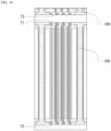
- FIG. 12A is a schematic top view showing the laser diode element according to an embodiment of the present invention.
- FIG. 12B is a cross-sectional view along the line XB-XB of FIG. 12A .
- the laser diode element 500 has the nitride semiconductor substrate 11, the first conductivity type semiconductor layer 12, the active layer 13, the second conductivity type semiconductor layer 14, the end face on the light emitting side 71, the end face on the light reflecting side 72, and the plurality of protrusions 20.
- the first conductivity type semiconductor layer 12 is provided on the nitride semiconductor substrate 11, the active layer 13 is provided on the first conductivity type semiconductor layer 12, and the second conductivity type semiconductor layer 14 is provided on the active layer 13.
- the protrusions 20 each have a first side surface 21 and a second side surface 22 that connect the end face on the light emitting side 71 and the end face on the light reflecting side 72 to the ridges 23, respectively.
- the ridges 23 are disposed between the first side surface 21 and the second side surface 22 in top view, and the direction intersecting the end face on the light emitting side 71 is the lengthwise direction.
- the lower end of the first side surface 21 and the lower end of the second side surface 22 are located below the lower surface of the active layer 13.
- the first distance D1 from the first side surface 21 to the ridge 23 at the end face on the light emitting side 71 is different from the second distance D2 from the second side surface 22 to the ridge 23.
- the first distance D1 is the same for all of the protrusions 20.
- the first distance D1 and the second distance D2 may use the end face on the light reflecting side 72 as their reference.
- the first protrusion 20a has a first region located on the side of the first side surface 21 side and a second region located on the second side surface 22 side, with the ridge 23 as a boundary between them.
- the first region of the first protrusion 20a has a first outer portion including the end face on the light emitting side 71, a second outer portion including the end face on the light reflecting side 72, and a first inner portion located between the first outer portion and the second outer portion. Regarding the width in the direction running along the end face on the light emitting side 71, the width of the first inner portion is greater than the width of the first outer portion and the width of the second outer portion.
- the second protrusion 20b has a first region located on the first side surface 21 side and a second region located on the second side surface 22 side, with the ridge 23 as a boundary between them.
- the second region of the second protrusion 20b has a third outer portion including the end face on the light emitting side 71, a fourth outer portion including the end face on the light reflecting side 72, and a second inner portion located between the third outer portion and the fourth outer portion.
- the width of the second inner portion is greater than the width of the third outer portion and the width of the fourth outer portion.
- an island portion is provided between the second inner portion and the end face on the light emitting side 71, and is separated from the second protrusion 20b.
- the laser diode element 500 can independently control the drive of each of the plurality of protrusions 20.
- the number of ridges had by the laser diode element 500 is 2 or more, but may be 3 or more, or may be 4 or more.
- the width of the laser diode element 500 in the direction running along the end face on the light emitting side 71 can be 600 ⁇ m or less, for example. This width can be 100 ⁇ m or more, for example.
- the length of the laser diode element 500 in the direction along the lengthwise direction of the ridges 23 can be 300 ⁇ m or more, and can be 2 mm or less, for example.
- the shape of the laser diode element 500 is rectangular, for example.
- the laser diode element 500 can emit a plurality of laser beams. These laser beams are ultraviolet light or visible light, for example.
- the peak wavelength of the laser beams may be 400 nm or more and 550 nm or less, for example.
- the plurality of laser beams in one laser diode element 500 are the same color, for example. For instance, in a plurality of laser beams in a single laser diode element 500, the difference between the longest peak wavelength and the shortest peak wavelength may be 5 nm or less.
- the shape, arrangement, material, and the like of the various members constituting the laser diode element 500 can be the same as what was described in the stacked body preparation step S 101.
- the planned cleavage lines 200 in the stacked body preparation step S101 can be read as either the end face on the light emitting side 71 or the end face on the light reflecting side 72 in the laser diode element 500 in the laser diode element 500.
- the planned division lines 300 in the stacked body preparation step S101 can be read as the outermost surface of the element.
- the mode in which the laser diode element 500 is used is not limited to a mode in which the upper surface is facing up as described in this embodiment, and any direction may be facing up.
- FIG. 13 is a schematic cross-sectional view showing the light emitting device according to an embodiment of the present invention.
- the light emitting device 600 has the laser diode element 500, a support 610, and a package 620.
- the support 610 is a member to which the laser diode element 500 is fixed and electrically connected, and is, for example, a submount.
- the support 610 includes a main body 611 and a conductive layer 612 provided on the surface of the main body.
- the main body 611 is a ceramic or other such insulating member.
- the second conductive layer 42 of the laser diode element 500 is joined to the conductive layer 612 of the support 610 via a conductive adhesive agent 630.
- the third conductive layer 43 of the laser diode element 500 may be joined to the conductive layer 612 of the support 610 via a conductive adhesive agent 630. This allows the heat generated by the laser diode element 500 to be dissipated to the support 610 via the third conductive layer 43.
- the package 620 is made of a conductive material such as metal or the like, or an insulating material such as glass, a ceramic or the like, or a composite material of the two. Part of the package 620 is light transmissive, so as to transmit the laser beam. The laser beam passes through the light-transmissive portion of the package 620 and is emitted outside the light emitting device 600. A wavelength conversion member such as a phosphor or the like may be disposed in the portion of the package 620 through which the laser beam passes. The package 620 airtightly seals the laser diode element 500.
- the package 620 has an anode and a cathode.
- the anode of the laser diode element 500 is electrically connected to the anode of the package via a conductive layer, a wire, or the like.
- the cathode of the laser diode element 500 is electrically connected to the cathode of the package via a conductive layer, a wire, or the like.
- the laser diode element of Example 1 and the laser diode elements of comparative examples are similar in that they have four protrusions on which one ridge is formed, but the laser diode elements were produced with different first distances D1 and second distances D2.
- the first distance D1 and the second distance D2 in the four protrusions were set to 34 ⁇ m and 14 ⁇ m, respectively.
- the first distance D1 and the second distance D2 in the four protrusions were set to 87 ⁇ m and 14 ⁇ m, 34 ⁇ m and 24 ⁇ m, 24 ⁇ m and 34 ⁇ m, and 14 ⁇ m and 87 ⁇ m.
- laser diode elements were obtained by carrying out the cleavage step and the Dividing step under the same conditions.
- FIG. 14 is a graph of the normal probability distribution of the measurement results.
- the data are plotted with the threshold current on the vertical axis and the cumulative probability on the horizontal axis.
- a black circle indicates a first protrusion of Example 1
- a white circle indicates a second protrusion of Example 1
- a gray triangle indicates a first protrusion of a comparative example
- a white triangle indicates a second protrusion of a comparative example.
- making the first distance D1 equal reduces variance in the characteristics of the plurality of laser beams corresponding to the plurality of ridges. It can also be seen from FIG. 14 that variance in the threshold current values of the plurality of laser diode elements in Example 1 is smaller than the variance of the threshold current values of the plurality of laser diode elements in the comparative examples. Because of this, it can be said that variance among the plurality of laser diode elements can be reduced by making the first distance D1 equal.
- Example 2 As shown in FIG. 7A , a plurality of the laser diode elements of Example 2 were produced in the same manner as in Example 1 except that an island portion was provided between the second inner portion and the planned cleavage line.
- the size of ripple in the FFP of the laser light emitted from each protrusion was checked, and any in which the size of ripple at or above a specific value was judged to have ripple.
- the incidence of the occurrence of ripple was calculated for each protrusion, the incidence of ripple was found to be the highest in the second protrusion.
- the size of ripple in the FFP of the laser light emitted by the second protrusion was checked, and it was determined whether or not there was ripple by the same criterion as for the laser diode elements of Example 1. As a result, none of the laser diode elements of Example 2 was determined to have ripple in the laser light of the second protrusion.
- the laser diode element described in the embodiments can be used, for example, as a light source for projectors, vehicle headlights, head-mounted displays, special lighting, displays, and the like.
Landscapes
- Physics & Mathematics (AREA)
- Condensed Matter Physics & Semiconductors (AREA)
- General Physics & Mathematics (AREA)
- Electromagnetism (AREA)
- Optics & Photonics (AREA)
- Geometry (AREA)
- Semiconductor Lasers (AREA)
Abstract
Description
- The present invention relates to a laser diode element and a method for manufacturing the same.
-
Patent Literature 1 describes an optically integrated semiconductor light emitting device having a plurality of light emitting device structures on a nitride semiconductor substrate. In the semiconductor light emitting device ofPatent Literature 1, the shape of the light emitting device structures is in line symmetry with respect to the center line of the semiconductor light emitting device. Also,Patent Literature 1 describes a GaN substrate as an example of a nitride semiconductor substrate, and indicates that the end face of the semiconductor light emitting device is formed by cleaving the GaN substrate. - Patent Literature 1:
Japanese Unexamined Patent Application Publication No. 2006-216772 - The shape of the end face formed by cleavage sometimes varies with the shape of the stacked body including the nitride semiconductor substrate. In a laser diode element that emits a plurality of laser beams, the greater is the variation in the shape of the end face of the portion corresponding to the optical waveguide of each laser beam, the greater is the variation in the characteristics of the plurality of laser beams in a given laser diode element.
- The present disclosure includes the following invention.
- A method for manufacturing a laser diode element, including:
- preparing a stacked body including a nitride semiconductor substrate, a first conductivity type semiconductor layer provided on the nitride semiconductor substrate, an active layer provided on the first conductivity type semiconductor layer, and a second conductivity type semiconductor layer provided on the active layer,
- in which the stacked body includes a plurality of element regions that are defined by a plurality of planned cleavage lines and a plurality of planned division lines intersecting the planned cleavage lines, in top view,
- the element region includes a plurality of protrusions each including a first side surface and a second side surface linking one of the planned cleavage lines and another of the planned cleavage lines, and a ridge that is disposed between the first side surface and the second side surface and whose lengthwise direction intersects the planned cleavage lines in top view,
- a lower end of the first side surface and a lower end of the second side surface are located below a lower surface of the active layer,
- a first distance on the planned cleavage line from the first side surface to the ridge is different from a second distance on the planned cleavage line from the second side surface to the ridge, in top view, and
- the first distances in one of the element regions are equal;
- cleaving the stacked body along the planned cleavage lines, in which a cleavage at each of the plurality of protrusions starts from the first side surface and reaches the second side surface; and
- dividing the stacked body along the planned division lines.
- A laser diode element, including:
- a nitride semiconductor substrate;
- a first conductivity type semiconductor layer provided on the nitride semiconductor substrate;
- an active layer provided on the first conductivity type semiconductor layer;
- a second conductivity type semiconductor layer provided on the active layer;
- an end face on the light emitting side;
- an end face on the light reflecting side; and
- a plurality of protrusions including a first side surface and a second side surface linking the end face on the light emitting side and the end face on the light reflecting side, and a ridge that is disposed between the first side surface and the second side surface in top view and whose lengthwise direction intersects the end face on the light emitting side,
- wherein the lower end of the first side surface and the lower end of the second side surface are located below the lower surface of the active layer,
- in top view, a first distance from the first side surface to the ridge at the end face on the light emitting side is different from a second distance from the second side surface to the ridge, and
- the first distances of the plurality of protrusions are equal.
- With the above-mentioned invention, it is possible to obtain a laser diode element in which variation in the characteristics of a plurality of laser beams corresponding to a plurality of ridges is reduced.
-
-
FIG. 1 is a flowchart showing the method for manufacturing a laser diode element according to an embodiment of the present invention; -
FIG. 2 is a schematic top view showing the method for manufacturing a laser diode element according to an embodiment of the present invention; -
FIG. 3 is a schematic top view of a stacked body showing a partial enlarged portion of the stacked body; -
FIG. 4A is a partial enlarged view ofFIG. 3 ; -
FIG. 4B is a cross-sectional view along the line IVB-IVB ofFIG. 4A ; -
FIG. 4C is a cross-sectional view along the line IVC-IVC ofFIG. 4A ; -
FIG. 5A is a schematic top view illustrating the shape of the protrusions; -
FIG. 5B is a schematic top view illustrating the shape of the protrusions; -
FIG. 6A is a schematic top view illustrating a modification of the shape of the protrusions; -
FIG. 6B is a partial enlarged view ofFIG. 6A ; -
FIG. 6C is a partial enlarged view ofFIG. 6A ; -
FIG. 7A is a schematic top view illustrating an example having island portions; -
FIG. 7B is a schematic top view illustrating another example having island portions; -
FIG. 8 is a schematic cross-sectional view illustrating a modification example of the stacked body; -
FIG. 9A is a schematic top view illustrating a modification example of the stacked body; -
FIG. 9B is a cross-sectional view along the line VIIB-VIIB ofFIG. 9A ; -
FIG. 9C is a cross-sectional view along the line VIIC-VIIC ofFIG. 9A ; -
FIG. 10 is a schematic top view showing the method for manufacturing a laser diode element according to an embodiment of the present invention; -
FIG. 11 is a schematic top view showing the method for manufacturing a laser diode element according to an embodiment of the present invention; -
FIG.12A is a schematic top view showing the laser diode element according to an embodiment of the present invention; -
FIG. 12B is a cross-sectional view along the line XB-XB ofFIG. 12A ; -
FIG. 13 is a schematic cross-sectional view showing the light emitting device according to an embodiment of the present invention; and -
FIG. 14 is a graph of the normal probability distribution of threshold current values in Example 1 and a comparative example. - An embodiment of the present invention will now be described with reference to the drawings. In the drawings, elements that are the same are numbered the same. Also, in each cross-sectional view, only the state of the cut surface is shown, and members not present on the cut surface are not shown.
-
FIG. 1 is a flowchart showing the method for manufacturing a laser diode element according to an embodiment of the present invention. As shown inFIG. 1 , the method for manufacturing a laser diode element of the present embodiment includes a stacked body preparation step S101, a cleavage step S 102, and a Dividing step S103.FIG. 2 to FIG. 12B are schematic views showing the method for manufacturing a laser diode element according to an embodiment of the present invention. - First, as shown in
FIG. 2 , astacked body 100 is prepared. Thestacked body 100 shown inFIG. 2 is a wafer. Thestacked body 100 includes a plurality ofelement regions 400 that are defined in top view by a plurality ofplanned cleavage lines 200 and a plurality ofplanned division lines 300 intersecting the planned cleavage lines 200. InFIG. 2 , the lines extending to the left and right in the drawing are the plannedcleavage lines 200, and the lines extending in the vertical direction in the drawing are the planned division lines 300. The plannedcleavage lines 200 and theplanned division lines 300 are both virtual lines. The plannedcleavage lines 200 and theplanned division lines 300 intersect at a right angle, for example. In top view, theelement regions 400 are rectangles, for example. InFIG. 2 , the ends of all theplanned cleavage lines 200 and theplanned division lines 300 are aligned with the outer edge of thestacked body 100, when the plannedcleavage lines 200 and/or theplanned division lines 300 may be absent in portions that do not complete a laser diode element. Thestacked body 100 may be a wafer as shown inFIG. 2 , or may be a divided piece obtained by dividing the wafer into a plurality of pieces. -
FIG. 3 is a schematic top view of a stacked body showing a partial enlarged portion of the stacked body. The pattern as shown inFIG. 3 is disposed in each of theelement regions 400. InFIG. 3 , all of theelement regions 400 have the same pattern. Some of theelement regions 400 may, however, have a different pattern. -
FIG. 4A is a partial enlarged view ofFIG. 3 ;FIG. 4B is a cross-sectional view along the line IVB-IVB ofFIG. 4A ;FIG. 4C is a cross-sectional view along the line IVC-IVC ofFIG. 4A . The line IVB-IVB inFIG. 4A coincides with a plannedcleavage line 200. That is,FIG. 4B is a cross-sectional view along a plannedcleavage line 200. - As shown in
FIG. 4A to FIG. 4C , thestacked body 100 includes anitride semiconductor substrate 11, a first conductivitytype semiconductor layer 12, anactive layer 13, and a second conductivitytype semiconductor layer 14. The first conductivitytype semiconductor layer 12 is provided on thenitride semiconductor substrate 11. Theactive layer 13 is provided on the first conductivitytype semiconductor layer 12. The second conductivitytype semiconductor layer 14 is provided on theactive layer 13. - For example, a GaN substrate is prepared as the
nitride semiconductor substrate 11. The readily cleavable plane of a nitride semiconductor having a Wurtzite structure, such as GaN and the like, is the m-plane (that is, the { 10-10} plane). In this case, the plannedcleavage lines 200 preferably coincide with the m-plane in top view. Consequently, cleavage can be performed very precisely along the planned cleavage lines 200. In this disclosure, the expression "coincide with the m-plane" is not limited to the case of exactly coinciding with the m-plane, and also includes a case in which the angle with respect to m-plane is 0.1 degree or less. For example, the upper surface of thenitride semiconductor substrate 11 may be the c-plane (that is, the (0001) plane or the (000-1) plane), and the plannedcleavage lines 200 are made to coincide with the m-plane. In this disclosure, the c-plane is not limited to a plane that exactly coincides with the (0001) plane or the (000-1) plane, and also includes planes having an off angle within the range of ± 0.03 to 1 degree. The shape of thenitride semiconductor substrate 11 is circular in top view, for example. A substrate having an orientation flat (OF) may be used as thenitride semiconductor substrate 11. If thenitride semiconductor substrate 11 is a substrate having an OF, the plannedcleavage lines 200 can be aligned with the m-plane by using the OF as a reference. - The semiconductor constituting the first conductivity
type semiconductor layer 12, theactive layer 13, and the second conductivitytype semiconductor layer 14 can be a nitride semiconductor, an example being a group III nitride semiconductor. Examples of group III nitride semiconductors include GaN, InGaN, and AlGaN. If the first conductivitytype semiconductor layer 12 is epitaxially grown on thenitride semiconductor substrate 11, and then theactive layer 13 and the second conductivitytype semiconductor layer 14 are epitaxially grown, their crystal orientations will be substantially the same. Consequently, the plannedcleavage lines 200 will coincide with the m-plane of thenitride semiconductor substrate 11, and therefore will also coincide with the m-plane of theactive layer 13 and the like above this. The first conductivitytype semiconductor layer 12 is an n-type semiconductor layer, for example. The second conductivitytype semiconductor layer 14 is a p-type semiconductor layer, for example. Thenitride semiconductor substrate 11, the first conductivitytype semiconductor layer 12, theactive layer 13, and the second conductivitytype semiconductor layer 14 may be in direct contact with each other, or another semiconductor layer may be disposed in between them. For example, an undoped layer may be disposed between the second conductivitytype semiconductor layer 14 and theactive layer 13. Theactive layer 13 can have a multiple quantum well structure or a single quantum well structure. Examples of the plurality of semiconductor layers formed on thenitride semiconductor substrate 11 include an n-side clad layer, an n-side optical guide layer, theactive layer 13, a p-side electron confinement layer, a p-side optical guide layer, a p-side clad layer, and a p-side contact layer, in that order starting from thenitride semiconductor substrate 11 side. For example, the n-side clad layer is the first conductivitytype semiconductor layer 12, and the p-side clad layer is the second conductivitytype semiconductor layer 14. The plurality of semiconductor layers including the first conductivitytype semiconductor layer 12, theactive layer 13, and the second conductivitytype semiconductor layer 14 can be formed, for example, by metal organic chemical vapor deposition (MOCVD). - Each of the plurality of
element regions 400 includes a plurality ofprotrusions 20. The number ofprotrusions 20 included in asingle element region 400 is two or more, and may be three or more. In the case of three or more, theprotrusions 20 in oneelement region 400 will include afirst protrusion 20a, asecond protrusion 20b, and one or moreintermediate protrusions 20c. Thefirst protrusion 20a is located on the side where the cleavage begins. Thesecond protrusion 20b is located on the side where the cleavage ends. InFIG. 4A to FIR. 4C, the right side in the drawing is the side where the cleavage begins, and the left side in the drawing is the side where the cleavage ends. That is, in the cleavage step (discussed below), cleavage proceeds from right to left in the drawing. Theintermediate protrusions 20c are located between thefirst protrusion 20a and thesecond protrusion 20b. The number of intermediate protrusions is two, for example. - The
protrusions 20 each have afirst side surface 21, asecond side surface 22, and aridge 23. Thefirst side surface 21 and thesecond side surface 22 are surfaces connecting the twoplanned cleavage lines 200 that definition asingle element region 400. In top view, thefirst side surface 21 and thesecond side surface 22 are connected to each other via two planned cleavage lines 200. In top view, the outer edge of oneprotrusion 20 is constituted by twoplanned cleavage lines 200, thefirst side surface 21, and thesecond side surface 22. Thefirst side surface 21 and thesecond side surface 22 may be inclined with respect to the upper surface of theprotrusion 20, in which case the outer edge of theprotrusion 20 can be defined using the upper end of thefirst side surface 21 and the upper end of thesecond side surface 22. In each of theprotrusions 20 shown inFIG. 4A to FIG.4C , the side surface on the right side in the drawing is thefirst side surface 21, and the side surface on the left side in the drawing is thesecond side surface 22. - The
ridges 23 are disposed between thefirst side surface 21 and thesecond side surface 22 in top view. In top view, the lengthwise direction of theridges 23 is a direction that intersects the planned cleavage lines 200. That is, theridges 23 have a long shape, and their lengthwise direction is a direction that intersects the planned cleavage lines 200. The lengthwise direction of theridges 23 may be parallel to the planned division lines 300. Theridges 23 are in the form of stripes, for example. An optical waveguide can be defined by theridges 23. For example, the portion of theactive layer 13 directly below theridges 23 and the peripheral portion thereof can be an optical waveguide. Since oneelement region 400 has a plurality ofridges 23, the laser diode element thus obtained has a plurality of optical waveguides. Theridges 23 are formed one for eachprotrusion 20, for example. Consequently, in the laser diode element thus obtained, drive control of the plurality of optical waveguides can be carried out independently. Theridges 23 are formed, for example, on part of the upper surface of the second conductivitytype semiconductor layer 14. Theprotrusions 20 including theridges 23 can be formed by removing a part of the semiconductor layers on thenitride semiconductor substrate 11 by using photolithography and etching, for example. - The lower end of the
first side surface 21 and the lower end of thesecond side surface 22 are located below the lower surface of theactive layer 13. Consequently, since theactive layer 13 of the plurality ofprotrusions 20 is divided, in the resulting laser diode element each of the plurality of optical waveguides corresponding to theprotrusions 20 can be driven individually. Also, since the lower end of thefirst side surface 21 is located below the lower surface of theactive layer 13, the end face constituting a part of the optical waveguide is formed by cleavage starting from thefirst side surface 21 in the cleavage step (discussed below). Therefore, the shape of theprotrusion 20 can affect the shape of the end face constituting a part of the optical waveguide. The lower end of thefirst side surface 21 and the lower end of thesecond side surface 22 are located, for example, in the first conductivitytype semiconductor layer 12. The upper end of thefirst side surface 21 and the upper end of thesecond side surface 22 are located, for example, in the second conductivitytype semiconductor layer 14. The second conductivitytype semiconductor layer 14 is disposed on each of the plurality ofprotrusions 20. The second conductivitytype semiconductor layer 14 on oneprotrusion 20 and the second conductivitytype semiconductor layer 14 on anotherprotrusion 20 are not linked and are separated from each other. In other words, oneelement region 400 can be said to include a plurality of second conductivity type semiconductor layers 14. Thus dividing the second conductivitytype semiconductor layer 14 makes it possible to independently control the drive of each of the plurality ofprotrusions 20. - As shown in
FIGS. 4A and4B , the distance between thefirst protrusion 20a and theplanned division line 300 can be made shorter than the distance between thesecond protrusion 20b and theplanned division line 300 on the plannedcleavage line 200. This asymmetry in distance can be used to distinguish between the portion on the light emitting side and the portion on the light reflecting side. Also, this asymmetry in distance can be used to distinguish between the end face on the light emitting side and the end face on the light reflecting side in the laser diode element after separation into individual pieces. -
FIG. 5A andFIG. 5B are schematic top views illustrating the shape of the protrusions.FIG. 5A is a view showing only theprotrusions 20, theridges 23, the plannedcleavage lines 200, and theplanned division lines 300 in the same region asFIG. 3 , andFIG. 5B showing these in the same region asFIG. 4A . InFIG. 5B , theprotrusions 20 are indicated by solid lines, and theridges 23 are indicated by broken lines. As shown inFIG. 5B , a first distance D1 from thefirst side surface 21 to theridge 23 on a plannedcleavage line 200 is different from a second distance D2 from thesecond side surface 22 to theridge 23 on a plannedcleavage line 200 in top view. The plurality of first distances D1 in oneelement region 400 are all equal. InFIG. 5B , there are four first distances D1, all of which are equal. - By making the first distances D1 equal, the distance from the start of cleavage in each
protrusion 20 to the portion corresponding to the optical waveguide can be made more uniform in the cleavage step discussed below. It is believed that this makes it possible for the shape of the end face formed in the cleavage step (discussed below) to be made more uniform in the portion corresponding to the optical waveguide of eachprotrusion 20. As a result, variation in the characteristics of the plurality of laser beams corresponding to the plurality of ridges of the obtained laser diode element can be reduced. Also, variation between the laser diode elements can be reduced. It should be noted that the phrase "the first distances D1 are equal" not only means that the first distances D1 are exactly the same, and also encompasses a difference of 1 µm or less between the smallest first distance D1 and the largest first distance D1. - Since the second distance D2 is the distance from the
ridge 23 to thesecond side surface 22 in the cleavage direction, the influence that the portion corresponding to the optical waveguide has on cleavage is believed to be less than that of the first distance D1. Therefore, the plurality of second distances D2 in asingle element region 400 need not be equal. InFIG. 5B , the second distances D2 are all equal. Making all of the second distances D2 equal is believed to make it possible for the shape of the end face formed in the cleavage step to be more uniform. - When the
first side surface 21 and theridge 23 are close to each other, the flatness of the portion of the end face formed in the cleavage step immediately below theridge 23 may suffer. Therefore, the first distance D1 is preferably 20 µm or more. On the other hand, the above-mentioned effect of having all the first distances D1 be the same is more easily obtained the closer thefirst side surface 21 and theridge 23 are together. Therefore, the first distance D1 is preferably less than 80 µm, and more preferably 50 µm or less. Also, the first distance D1 is preferably greater than the second distance D2. This allows the width of theprotrusion 20 in the direction running along the plannedcleavage line 200 to be reduced while still obtaining the effect of having the first distances D1 be uniform. Reducing the width of theprotrusion 20 makes it possible to reduce the width of the obtained laser diode element. The second distance D2 can be 5 µm or more. The second distance D2 can be less than 50 µm, and is preferably less than 20 µm. This makes it possible for the laser diode element to be made more compact. - The width of the
protrusion 20 in the direction along the plannedcleavage line 200 can be 20 µm or more, for example. The shortest distance between twoadjacent protrusions 20 in oneelement region 400 can be 1 µm or more, for example, and is preferably 2 µm or more. This reduces the possibility of short-circuiting betweenadjacent protrusions 20. The distance betweenprotrusions 20 refers to the distance between the outer edge of oneprotrusion 20 and the outer edge of theother protrusion 20 in top view. In order to further reduce the possibility of a short circuit, it is preferable to provide an insulatingfilm 30 on the side surfaces of theprotrusions 20 as shown inFIGS. 4B and 4C . The width of aprotrusion 20 in the direction running along the plannedcleavage line 200 can be 150 µm or less, and can be 50 µm or less. This makes it possible for the laser diode element to be more compact. - In top view, a
protrusion 20 has a first region located on the side of thefirst side surface 21, and a second region located on the side of thesecond side surface 22, with aridge 23 serving as a boundary. Theprotrusion 20 may have an outer portion and an inner portion having different widths in the direction running along the plannedcleavage line 200. The outer portion is the portion of theprotrusion 20 through which the plannedcleavage line 200 passes. The inner portion is located between the two outer portions through which pass twoplanned cleavage lines 200 that define oneelement region 400. - As shown in
FIG. 5A , the first region of thefirst protrusion 20a has a firstouter portion 24a through which one of the plannedcleavage lines 200 passes, and a secondouter portion 24b through which another of the plannedcleavage lines 200 passes. The first region of thefirst protrusion 20a further has a firstinner portion 24c located between the firstouter portion 24a and the secondouter portion 24b. InFIG. 5A , the firstouter portion 24a and the secondouter portion 24b are indicated by cross-hatching, and the firstinner portion 24c is indicated by diagonal hatching. Regarding the width in the direction running along the plannedcleavage lines 200, the width of the firstinner portion 24c is greater than the width of the firstouter portion 24a and the width of the secondouter portion 24b. Since the width of the first region of thefirst protrusion 20a does not affect the distance betweenadjacent ridges 23 in oneelement region 400, this wide firstinner portion 24c may be provided to the first region of thefirst protrusion 20a. InFIG. 5A , the first region of thefirst protrusion 20a consists only of the firstouter portion 24a, the secondouter portion 24b, and the firstinner portion 24c. The first region of thefirst protrusion 20a may have a portion other than these. Thefirst protrusion 20a does not have to have the firstinner portion 24c. The top view shape of thefirst protrusion 20a may be the same as the top view shape of theintermediate protrusion 20c. - Regarding the length of the
ridge 23 in the lengthwise direction, the length of the firstinner portion 24c is greater than the length of each of the firstouter portion 24a and the secondouter portion 24b. Also, this length is greater than the combined length of the firstouter portion 24a and the secondouter portion 24b. This allows the firstinner portion 24c to be used as a portion where the firstconductive layer 41 is mainly provided. The length of the firstinner portion 24c can be half or more of the length of theridge 23, and may be 95% or more. The length of the firstinner portion 24c can be made less than the length of theridge 23, and may be 98% or less. - The second region of the
second protrusion 20b has a thirdouter portion 25a through which one of the plannedcleavage lines 200 passes, and a fourthouter portion 25b through which another of the plannedcleavage lines 200 passes. The second region of thesecond protrusion 20b further has a secondinner portion 25c located between the thirdouter portion 25a and the fourthouter portion 25b. InFIG. 5A , the thirdouter portion 25a and the fourthouter portion 25b are indicated by cross-hatching, and the secondinner portion 25c is indicated by diagonal hatching. Regarding the width in the direction running along the plannedcleavage lines 200, the width of the secondinner portion 25c is greater than the width of the thirdouter portion 25a and the width of the fourthouter portion 25b. For the same reason as with the first region of thefirst protrusion 20a, this wide secondinner portion 25c may be provided in the second region of thesecond protrusion 20b. InFIG. 5A , the second region of thesecond protrusion 20b consists only of the thirdouter portion 25a, the fourthouter portion 25b, and the secondinner portion 25c. The second region of thesecond protrusion 20b may have a portion other than these. Thesecond protrusion 20b does not have to have the secondinner portion 25c. In that case, the thirdconductive layer 43 discussed below need not be provided. The top view shape of thesecond protrusion 20b may be the same as the top view shape of theintermediate protrusion 20c. - Regarding the length of the
ridge 23 in the lengthwise direction, the length of the secondinner portion 25c is greater than the length of each of the thirdouter portion 25a and the fourthouter portion 25b, and this length is greater than the combined length of the thirdouter portion 25a and the fourthouter portion 25b. This allows the secondinner portion 25c to be used as a portion where the firstconductive layer 41 is mainly provided. The length of the secondinner portion 25c can be half or more of the length of theridge 23, and may be 95% or more. The length of the secondinner portion 25c can be made less than the length of theridge 23, and may be 98% or less. - The region in which the first
outer portion 24a and the thirdouter portion 25a are provided and which is sandwiched between the firstouter portion 24a of oneelement region 400 and the thirdouter portion 25a of anotherelement region 400 that is opposite the oneelement region 400 may be used as a region for forming a groove in the cleavage step discussed below. Oneelement region 400 and anotherelement region 400 are, for example, twoelement regions 400 disposed side by side in the horizontal direction inFIG. 5A . Also, a region in which the secondouter portion 24b and the fourthouter portion 25b are provided and which is sandwiched between the secondouter portion 24b of oneelement region 400 and the fourthouter portion 25b of anotherelement region 400 that is opposite the oneelement region 400 may be used as a region for forming a groove in the cleavage step discussed below. -
FIG. 6A is a schematic top view illustrating a modification of the shape of theprotrusions 20. As shown inFIG. 6A , the distance between theprotrusions 20 on the plannedcleavage line 200 may be greater than the shortest distance between theprotrusions 20. InFIG. 6A , on the plannedcleavage line 200, thefirst side surface 21 and thesecond side surface 22 are each provided with a concave shape that is recessed toward theridge 23. Consequently, deviation between the position actually cleaved in the cleavage step and the plannedcleavage line 200 can be reduced. This concave shape may also be provided only to either thefirst side surface 21 or thesecond side surface 22, and in order to more reliably reduce deviation between the actual cleavage position and the plannedcleavage line 200, it is preferable to provide this shape to both. InFIG. 6A , the first distance D1 is the distance from theridge 23 to the side of the concave shape closest to theridge 23, and the second distance D2 is the distance from theridge 23 to the side of the concave shape closest to theridge 23. - The
protrusions 20 shown inFIG. 6A can be said to have a structure having an intermediate portion between the outer portion and the inner portion. Regarding the width in the direction running along the plannedcleavage line 200, the width of the middle portion is greater than the width of the outer portion and less than the width of the inner portion. -
FIG. 6B is an enlarged view of a portion of thefirst protrusion 20a in the vicinity of the line of the plannedcleavage line 200. As shown inFIG. 6B , thefirst protrusion 20a has anintermediate portion 24d between the firstouter portion 24a and the firstinner portion 24c. The width W24a of the firstouter portion 24a coincides with the first distance D1. The relation between the width W24a of the firstouter portion 24a, the width W24c of the firstinner portion 24c, and the width W24d of theintermediate portion 24d is W24a < W24d < W24c. The relation between these widths can satisfy (W24d-W24a) < (W24c-W24d). As shown inFIG. 6A , providing theintermediate portion 24d allows the portion between theintermediate portion 24d of oneelement region 400 and theintermediate portion 24d of anotherelement region 400 adjacent thereto, with the plannedcleavage line 200 in between, to be used as a portion that guides the progress of cleavage. In order to use this portion as such a guide, the length in a direction running along the lengthwise direction of theridge 23 is preferably such that the relation between the length L24a of the firstouter portion 24a and the length L24d of theintermediate portion 24d is L24a < L24d. The length of the firstinner portion 24c may be greater than the length L24d of theintermediate portion 24d. -
FIG. 6C is an enlarged view of a portion of thesecond protrusion 20b in the vicinity of the line of the plannedcleavage line 200. Thesecond protrusion 20b has anintermediate portion 25d between the thirdouter portion 25a and the secondinner portion 25c. The width W25a of the thirdouter portion 25a coincides with the second distance D2. The relation between the width W25a of the thirdouter portion 25a, the width W25c of the secondinner portion 25c, and the width W25d of theintermediate portion 25d is W25a < W25d < W25c. The relation between these widths can satisfy (W25d-W25a) < (W25c -W25d). As shown inFIG. 6A , providing theintermediate portion 25d allows the portion between theintermediate portion 25d of oneelement region 400 and theintermediate portion 25d of anotherelement region 400 adjacent thereto, with the plannedcleavage line 200 in between, to be used as a portion that guides the progress of cleavage. In order to use this portion as such a guide, the length in a direction running along the lengthwise direction of theridge 23 is preferably such that the relation between the length L25a of the thirdouter portion 25a and the length L25d of theintermediate portion 25d is L25a < L25d. The length of the secondinner portion 25c may be greater than the length L25d of theintermediate portion 25d. - As shown in
FIG. 6A , the second region of thefirst protrusion 20a can have an outer portion and an inner portion having different widths in the direction running along the plannedcleavage line 200. The second region of thefirst protrusion 20a does not have an intermediate portion, and the outer portion and the inner portion are directly connected together. The width of the outer portion of the second region of thefirst protrusion 20a coincides with the second distance D2. The difference between the width of the outer portion and the width of the inner portion in the second region of thefirst protrusion 20a may be the same as the difference between the width of the firstouter portion 24a and the width of theintermediate portion 24d in the first region of thefirst protrusion 20a. Regarding the length of theridge 23 in the lengthwise direction, the length of the outer portion of the second region of thefirst protrusion 20a can be the same as the length of the firstouter portion 24a. - As shown in
FIG. 6A , the first region of thesecond protrusion 20b can have an outer portion and an inner portion having different widths in the direction running along the plannedcleavage line 200. The first region of thesecond protrusion 20b does not have an intermediate portion, and the outer portion and the inner portion are directly connected together. The width of the outer portion of the first region of thesecond protrusion 20b coincides with the first distance D1. The difference between the width of the outer portion and the width of the inner portion in the first region of thesecond protrusion 20b may be the same as the difference between the width of the thirdouter portion 25a and the width of theintermediate portion 25d in the second region of thesecond protrusion 20b. Regarding the length of theridge 23 in the lengthwise direction, the length of the outer portion of the first region of thesecond protrusion 20b can be the same as the length of the thirdouter portion 25a. - As shown in
FIG. 6A , the first region of theintermediate protrusion 20c can have an outer portion and an inner portion having different widths in the direction running along the plannedcleavage line 200. The first region of theintermediate protrusion 20c does not have an intermediate portion, and the outer portion and the inner portion are directly connected together. The width of the outer portion of the first region of theintermediate protrusion 20c coincides with the first distance D1. The difference between the width of the outer portion and the width of the inner portion in the first region of theintermediate protrusion 20c may be the same as the difference between the width of the firstouter portion 24a of thefirst protrusion 20a and the width of theintermediate portion 24d. Regarding the length along the lengthwise direction of theridge 23, the length of the outer portion of the first region of theintermediate protrusion 20c can be the same as the length of the firstouter portion 24a of thefirst protrusion 20a. - As shown in
FIG. 6A , the second region of theintermediate protrusion 20c can have an outer portion and an inner portion having different widths in the direction running along the plannedcleavage line 200. The second region of theintermediate protrusion 20c does not have an intermediate portion, and the outer portion and the inner portion are directly connected together. The width of the outer portion of the second region of theintermediate protrusion 20c coincides with the second distance D2. The difference between the width of the outer portion and the width of the inner portion in the second region of theintermediate protrusion 20c may be the same as the difference between the width of the thirdouter portion 25a and the width of theintermediate portion 25d of thesecond protrusion 20b. Regarding the length along the lengthwise direction of theridge 23, the length of the outer portion of the second region of theintermediate protrusion 20c can be the same as the length of the thirdouter portion 25a of thesecond protrusion 20b. - As shown in
FIG. 6A , the length of the outer portion may be the same in all theprotrusions 20. InFIG. 6A , an intermediate portion is provided only in the first region of thefirst protrusion 20a and the second region of thesecond protrusion 20b, located between theplanned division line 300 and theridge 23, and the other regions are not provided with intermediate portions. Consequently, the width of the laser diode element thus obtained can be reduced. -
FIG. 7A is a schematic top view illustrating an example having island portions.FIG. 7A is an enlarged view of a portion of thesecond protrusion 20b in the vicinity of the line of the plannedcleavage line 200. InFIG. 7A , the insulatingfilm 30 and the like are omitted as inFIG. 6C . As shown inFIG. 7A , theelement region 400 includes anisland portion 26 that is separated from thesecond protrusion 20b, between the secondinner portion 25c and at least one of the planned cleavage lines 200. Theisland portion 26 can be formed by removing part of the plurality of semiconductor layers on thenitride semiconductor substrate 11 by using photolithography and etching, for example. - Providing the
island portion 26 allows the ripple produced in the far field pattern (FFP) of the resulting laser diode element to be reduced. Theother protrusions 20 are disposed to the side of the second region of thefirst protrusion 20a and theintermediate protrusion 20c, and no protrusion is disposed to the side of the second region of thesecond protrusion 20b. In other words, the second region of thefirst protrusion 20a and theintermediate protrusion 20c is sandwiched between a ridge and anotherprotrusion 20, and the second region of thesecond protrusion 20b is not in such a positional relation. Therefore, particularly in a structure in which the second distance D2 is less than the first distance D1, the amount of light that leaks from the second region of thesecond protrusion 20b when the obtained laser diode element is driven tends to be larger than the amount of light that leaks from the first region of thesecond protrusion 20b. Also, the amount of light that leaks from the second region of thesecond protrusion 20b tends to be larger than the amount of light that leaks from the first region and the second region of thefirst protrusion 20a and theintermediate protrusion 20c. These tendencies are more pronounced when the secondinner portion 25c is provided. In view of this, by providing theisland portion 26, the second distance D2 can be maintained while absorbing or scattering the light that leaks from the second region of thesecond protrusion 20b. Therefore, the ripple produced in the FFP of the obtained laser diode element can be reduced. - In order to reduce the ripple of FFP more efficiently, the
island portion 26 is preferably provided near the plannedcleavage line 200. The shortest distance between theisland portions 26 and the plannedcleavage line 200 can be 3 µm or less, for example. Also, theisland portion 26 is provided so as to be located between the end face on the light emitting side and the secondinner portion 25c in the obtained laser diode element. Theisland portion 26 may instead be provided so as to be located between the end face on the light reflecting side and the secondinner portion 25c. Oneelement region 400 may have anisland portion 26 between one of the plannedcleavage lines 200 and the secondinner portion 25c, and one between another of the plannedcleavage lines 200 and the secondinner portion 25c. Theisland portion 26 may be provided to thesecond protrusion 20b that does not have the secondinner portion 25c. In this case, theisland portion 26 is disposed between thesecond protrusion 20b and the adjacentplanned division line 300. Theisland portion 26 may be provided between theplanned cleavage line 200 and the firstinner portion 24c of thefirst protrusion 20a. In the case that the goal is to reduce ripple in the FFP of the laser beam emitted by thesecond protrusion 20b, theisland portion 26 may not be provided between the firstinner portion 24c of thefirst protrusion 20a and the plannedcleavage line 200, and may be provided only between the secondinner portion 25c of thesecond protrusion 20b and the plannedcleavage line 200. Also, theisland portion 26 need not be provided between theintermediate protrusion 20c and the plannedcleavage line 200. - In the case that a groove formed by using a laser scribing device or the like reaches the
island portion 26 in the cleavage step discussed below, there is the possibility of short-circuiting between the p-type semiconductor layer and the n-type semiconductor layer of theisland portion 26. Therefore, theisland portion 26 is preferably provided away from thesecond protrusion 20b. The lower end of theisland portion 26 is located below the lower surface of theactive layer 13. The shortest distance between theisland portion 26 and the secondinner portion 25c can be set to be greater than the shortest distance between theisland portion 26 and the plannedcleavage line 200. - Regarding the width in the direction running along the planned
cleavage line 200, the width of theisland portion 26 may be less than the width of the secondinner portion 25c. For example, in the case that a line parallel to the plannedcleavage line 200 is superimposed with theisland portion 26 in top view, the width of theisland portion 26 can be set so that the distance between theridge 23 and the farthest end of theisland portion 26 from theridge 23 on this line is equal to the distance between theridge 23 and thefirst side surface 21 of thefirst protrusion 20a. This is expected to reduce the difference in the FFP between the laser light emitted from thefirst protrusion 20a and the laser light emitted from thesecond protrusion 20b in the resulting laser diode element. It should be noted that saying that the distances are equal encompasses a case in which the difference between the distances is 1 µm or less. The width of theisland portion 26 can be 95% or less of the width of the secondinner portion 25c, and furthermore can be 40% or less. The width of theisland portion 26 can be 20% or more of the width of the secondinner portion 25c, and furthermore can be 30% or more. - There may be just one
island portion 26, but as shown inFIG. 7A , theisland portion 26 may include afirst portion 26a and asecond portion 26b. In top view, thesecond portion 26b is separated from thefirst portion 26a and is located between thefirst portion 26a and the secondinner portion 25c. Since theisland portion 26 is thus composed of a plurality of portions, there is a higher probability that light will be reflected due to the difference in refractive index between each portion and the outside thereof (for example, the insulatingfilm 30, air or the like), so the ripples in the FFP can be effectively reduced. Of the side surface of thefirst portion 26a and the side surface of thesecond portion 26b, at least the portions opposite each other are preferably located below the lower surface of theactive layer 13. This further reduces ripples in the FFP. The shortest distance between thefirst portion 26a and thesecond portion 26b is 2 µm or less, for example. The shortest distance between thefirst portion 26a and thesecond portion 26b is 0.5 µm or more, for example. - In
FIG. 7A , thefirst portion 26a and thesecond portion 26b are separated by a wavy groove, and the bottom of the groove is located below the lower surface of theactive layer 13. The wavy groove can be said to have a first constituent side and a second constituent side having different inclination angles with respect to the resonance surface in top view. Providing the first constituent side and the second constituent side allows leaked light to be refracted in two different directions. Therefore, the concentration of refracted light leakage in a specific direction can be moderated. The top view shape of the groove can also be described as the portion where the outer edge of thefirst portion 26a and the outer edge of thesecond portion 26b are facing each other. The groove separating thefirst portion 26a and thesecond portion 26b does not have to be wavy. - In
FIG. 7A , part of thefirst side surface 21 and thesecond side surface 22 of thesecond protrusion 20b has a shape extending toward theridge 23. Thus providing a concave portion that is recessed downward near theridge 23 on the light emitting side further reduces the ripples that are produced in the FFP of the resulting laser diode element. In the case where a groove is thus provided to thesecond protrusion 20b, the groove that separates thefirst portion 26a and thesecond portion 26b may be disposed on an extension line of the groove. InFIG. 7A , the groove provided to thesecond protrusion 20b has a wavy shape in top view. -
FIG. 7B is a schematic top view illustrating another example havingisland portions 26. InFIG. 7B , a third distance between theridge 23 and the end of theisland portion 26 that is farthest from theridge 23 of thesecond protrusion 20b is equal to a fourth distance between theridge 23 and the end of the secondinner portion 25c that is farthest from theridge 23 of theprotrusion 20b. Equal of the third distance and the fourth distance encompasses a case in which the difference between these widths is 1 µm or less. The third distance may be greater than the fourth distance. Making the third distance be equal to or greater than the fourth distance further reduces the ripples in the FFP of the laser light emitted from thesecond protrusion 20b in the resulting laser diode element. In the case where the resulting laser diode element is mounted in a package and sealed, the incidence of ripples in the FFP of the laser beam emitted by the laser diode element may increase after sealing as compared with that before mounting. If this happens, the incidence of ripples in the FFP of the laser beam emitted by thesecond protrusion 20b after the package is sealed can be reduced more reliably by making the third distance equal to or greater than the fourth distance. - As shown in
FIG. 7B , theelement regions 400 can have anisland portion 27 separated that is from thefirst protrusion 20a, between the firstinner portion 24c and at least one of the planned cleavage lines 200. Providing theisland portion 27 reduces the ripples produced in the FFP of the obtained laser diode element. Theisland portion 27 can be formed, for example, by removing some of the plurality of semiconductor layers on thenitride semiconductor substrate 11 by photolithography and etching. InFIG. 7B , in top view, a fifth distance between theridge 23 and the end of theisland portion 27 that is farthest from theridge 23 of thefirst protrusion 20a is equal to a sixth distance between theridge 23 and the end of the firstinner portion 24c that is farthest from theridge 23 of theprotrusion 20a. Equal of the fifth distance and the sixth distance encompasses a case in which the difference between these widths is 1 µm or less. The fifth distance may be greater than the sixth distance. Making the fifth distance equal to or larger than the sixth distance more reliably reduces the incidence of ripples in the FFP of the laser beam emitted from thefirst protrusion 20a after the package is sealed. - In
FIG. 7B , the third distance between theridge 23 and the end of theisland portion 26 that is farthest from theridge 23 of thesecond protrusion 20b is equal to the fifth distance between theridge 23 and the end of theisland portion 27 that is farthest from theridge 23 of thefirst protrusion 20a. This is expected to reduce the difference in the FFP between the laser light emitted from thefirst protrusion 20a and the laser light emitted from thesecond protrusion 20b in the resulting laser diode element. Equal of the third distance and the fifth distance encompasses a case in which the difference between the distances is 1 µm or less. - In
FIG. 7B , the first distance D1 from thefirst side surface 21 to theridge 23 is equal to the second distance D2 from thesecond side surface 22 to theridge 23, on the planned cleavage lines 200. Equal of the first distance D1 and the second distance D2 encompasses a case in which the difference between the distances is 1 µm or less. In the case where the first distance D1 and the second distance D2 are equal, it is preferable to provide both theisland portion 26 and theisland portion 27. Consequently, the difference in the FFP between the laser light emitted from thefirst protrusion 20a and the laser emitted from thesecond protrusion 20b in the obtained laser diode element can be reduced as compared to a case in which only one of theisland portion 26 and theisland portion 27 is provided. The shape of theisland portion 26 and theisland portion 27 may be a shape having a first portion and a second portion as shown inFIG. 7A . - In top view, the
protrusions 20 each have a first region located on thefirst side surface 21 side and a second region located on thesecond side surface 22 side, with theridge 23 as a boundary between them. As shown inFIGS. 4A and4C , theelement regions 400 include a plurality of firstconductive layers 41 disposed above the first region and therespective ridges 23 of the plurality ofprotrusions 20. The firstconductive layer 41 is electrically connected to the second conductivitytype semiconductor layer 14. The firstconductive layers 41 may also be formed in the second region. In the case where theprotrusions 20 have an outer portion and an inner portion as discussed above, the firstconductive layers 41 can be provided mainly on the inner portion. - The first
conductive layers 41 can be formed, for example, by stacking one or more layers of Ni, Rh, Cr, Au, W, Pt, Ti, Al, Pd or another such metal or alloy. The firstconductive layers 41 are formed, for example, by stacking a Ni layer, a Pd layer, a Au layer, a Pt layer, a Au layer, a Pt layer in that order. As shown inFIGS. 4A and4C , in the case where the secondconductive layer 42 is provided on the firstconductive layers 41, it is preferable for the outermost surface of the firstconductive layer 41 not to contain gold. Consequently, in the case where a joining material containing gold, such as AuSn or the like, is used as a conductive joining material for electrically connecting the laser diode element to the conductive layer of a submount and the like, the joining material will be less likely to adhere to the outermost surface of the firstconductive layer 41. Therefore,protrusions 20 that are adjacent via a firstconductive layer 41 are less likely to short-circuit. The outermost surface of the firstconductive layer 41 is preferably made of a material that functions as a barrier layer with respect to the metal joining material for joining the laser diode element, such as a platinum layer. - In top view, the shapes of the first
conductive layers 41 of the plurality ofprotrusions 20 do not all have to be the same. In this embodiment, theelement regions 400 are all disposed in the same orientation. That is, inFIG. 4A , the lower side in the drawing is the light emitting side and the upper side in the drawing is the light reflecting side, with a plannedcleavage line 200 as the boundary in between them. InFIG. 4A , thefirst protrusion 20a and thesecond protrusion 20b are such that the shape of the firstconductive layers 41 on the light emitting side portion and the light reflecting side portion is in line symmetry with respect to the planned cleavage lines 200. On the other hand, in theintermediate protrusion 20c, the shape of the firstconductive layers 41 on the light emitting side portion and the light reflecting side portion is not in line symmetry with respect to the planned cleavage lines 200. Thus, in one or more of theprotrusions 20, the shape of the firstconductive layers 41 on the light emitting side portion and the light reflecting side portion may be asymmetrical with respect to the planned cleavage lines 200. This makes it easier to determine which is the light emitting side portion and which is the light reflecting side portion. Also, the top view shape of the firstconductive layers 41 is preferably asymmetric in 180-degree rotation around the center of theelement regions 400. This makes it easier to determine which is the light emitting side surface and which is the light reflecting side surface in the obtained laser diode element. - As shown in
FIG. 4C ,upper electrodes 50 may be provided between the firstconductive layers 41 and the second conductivitytype semiconductor layer 14. InFIG. 4C ,ridges 23 are formed on a part of the upper surface of the second conductivitytype semiconductor layer 14, and theupper electrodes 50 are formed in contact with the upper surfaces of theridges 23. Theupper electrodes 50 are p electrodes, for example. Examples of theupper electrodes 50 include a single-layer film or a multilayer film of Ni, Rh, Cr, Au, W, Pt, Ti, Al or other such metal or alloy, or a conductive oxide and the like containing at least metal selected from among zinc, indium, and tin. Examples of conductive oxides include ITO (indium tin oxide). As shown inFIGS. 4A and4B , theupper electrodes 50 can be formed, for example, so as to avoid the planned cleavage lines 200. - The
element regions 400 can include a plurality of secondconductive layers 42 disposed above the respective firstconductive layers 41. The secondconductive layer 42 is electrically connected to the firstconductive layer 41. As shown inFIG. 4A , the width of the secondconductive layer 42 is preferably less than the width of the firstconductive layer 41, the width in the direction running along the planned cleavage lines 200. Consequently, the shortest distance between the secondconductive layers 42 ofadjacent protrusions 20 can be made greater than the shortest distance between the firstconductive layers 41 ofadjacent protrusions 20, making it less likely thatadjacent protrusions 20 will short-circuit. In particular, such an arrangement is preferable in the case of performing flip-chip bonding, in which the secondconductive layers 42 are mounted on a submount and the like. - In
FIGS. 3 and4A , the outer edges of the secondconductive layers 42 are located inside the outer edges of the firstconductive layers 41 in top view. Also, the outer edges of the secondconductive layers 42 are located to the inside of the outer edges of the first region in top view. Thus, it is preferable for the secondconductive layer 42 to be disposed so as to avoid the upper parts of theridges 23. If the secondconductive layers 42 are formed on a step such as aridge 23, the film thickness may be uneven or partial separation may occur, but this will be less likely to happen if the secondconductive layers 42 are formed on a relatively flat surface that does not include anyridges 23. - The second
conductive layers 42 can be formed, for example, by stacking one or more layers of Ni, Rh, Cr, Au, W, Pt, Ti, Al or another such metal or alloy. The secondconductive layers 42 are formed, for example, by stacking a Ti layer, a Pt layer, a Au layer in that order. It is preferable for the outermost surface of the secondconductive layers 42 to be a gold layer or another such layer containing gold, so as to facilitate joining to a conductive bonding material such as AuSn or the like. - In
FIG. 4A , the firstconductive layer 41 disposed above thesecond protrusion 20b is also disposed above the second region of thesecond protrusion 20b. Theelement regions 400 can include a thirdconductive layer 43 disposed above the second region of thesecond protrusion 20b. The thirdconductive layers 43 can be formed, for example, by stacking one or more layers of Ni, Rh, Cr, Au, W, Pt, Ti, Al or another such metal or alloy. The thirdconductive layers 43 are formed, for example, by stacking a Ti layer, a Pt layer, a Au layer in that order. The thirdconductive layer 43 may be formed together with the secondconductive layer 42, from the same material and in the same film thickness as the secondconductive layer 42. As shown inFIGS. 4A and4B , the firstconductive layers 41, the secondconductive layers 42, and the thirdconductive layer 43 can be formed so as to avoid the planned cleavage lines 200. - In
FIGS. 3 and4A , the outer edge of the thirdconductive layer 43 is located to the inside of the outer edges of the firstconductive layers 41 in top view. Also, the outer edge of the thirdconductive layer 43 is located to the inside of the outer edge of the second region of thesecond protrusion 20b in top view. Thus, it is preferable for the thirdconductive layer 43 to be disposed so as to avoid the upper parts of theridges 23. If the thirdconductive layer 43 is formed on a step such as aridge 23, the film thickness may be uneven or partial separation may occur, but this will be less likely to happen if the thirdconductive layer 43 is formed on a relatively flat surface that does not include anyridges 23. Providing the thirdconductive layer 43 allows the heat generated when the obtained laser diode element is driven to be dissipated to a support or the like discussed below via the thirdconductive layer 43, so the heat dissipation is improved. - The maximum width of the
first protrusion 20a in the direction running along the plannedcleavage lines 200 can be made greater than the maximum width of theintermediate protrusion 20c in the direction running along the planned cleavage lines 200. Consequently, regarding the width of the external connection portion, such as the secondconductive layer 42, in the direction running along the plannedcleavage lines 200, the width of the external connection portion in thefirst protrusion 20a can be made greater than the width of the external connection portion in theintermediate protrusion 20c. This makes it easier to bring an inspection instrument such as an inspection needle and the like of a probe device used for inspection prior to mounting into contact with the external connection portion of thefirst protrusion 20a. For the same reason as with thefirst protrusion 20a, the maximum width of thesecond protrusion 20b in the direction running along the plannedcleavage lines 200 can be set greater than the maximum width of theintermediate protrusion 20c in the direction running along the planned cleavage lines 200. For example, regarding the width in the direction running along the plannedcleavage lines 200, the width of the secondconductive layer 42 and the width of the thirdconductive layer 43 of thefirst protrusion 20a are greater than the width of the secondconductive layer 42 of theintermediate protrusion 20c and the width of the secondconductive layer 42 of thesecond protrusion 20b. -
FIG. 8 is a schematic cross-sectional view illustrating a modification example of the stacked body. As shown inFIG. 8 , the secondconductive layer 42 may be disposed above theridge 23. In this case, the thirdconductive layer 43 need not be provided. Such an arrangement may be advantageous in order to reduce the width of the obtained laser diode element that is obtained. As shown inFIG. 8 , one end of the secondconductive layer 42 disposed on theintermediate protrusion 20c may be aligned with one end of the firstconductive layer 41. Aligning the end of the firstconductive layer 41 and the end of the secondconductive layer 42 located between theridge 23 and thesecond side surface 22 increases the surface area of the secondconductive layer 42 as compared with the case where these are not aligned. Consequently, when the heat generated by driving the resulting laser diode element is dissipated to the support or the like discussed below via the secondconductive layer 42, this dissipation will be more efficient. - As shown in
FIG. 7B , in the case where the secondconductive layer 42 is disposed above theridge 23, the width in top view of the secondconductive layer 42 provided on each of the plurality ofprotrusions 20 along the plannedcleavage lines 200 can all be set to be equal. In top view, the lengths of the secondconductive layers 42 provided to the plurality ofprotrusions 20 along the planneddivision lines 300 can all be set to be equal. Saying that the widths or lengths of the plurality of secondconductive layers 42 are equal encompasses not only a case where they are exactly the same, but also that the difference between the maximum value and the minimum value of the plurality of widths or lengths is 1 µm or less. As shown inFIG. 7B , in the case where the secondconductive layer 42 is disposed above theridge 23, the second distance D2 may be equal to the first distance D1. Saying that "the second distance D2 is equal to the first distance D1" encompasses not only a case where they are exactly the same, but also that the difference between the first distance D1 and the second distance D2 is 1 µm or less. Here again, the plurality of first distances D1 in oneelement region 400 are all equal. Consequently, it is possible to reduce variance in the characteristics of the plurality of laser beams corresponding to the plurality of ridges of the resulting laser diode element. Also, it is possible to reduce variance among a plurality of laser diode elements. -
FIG. 9A is a schematic top view illustrating a modification example of the stacked body.FIG. 9B is a cross-sectional view along the line VIIB-VIIB ofFIG. 9A .FIG. 9C is a cross-sectional view along the line VIIC-VIIC ofFIG. 9A. FIG. 9A is a detail view of a portion of anelement region 400 on the light emitting side of thefirst protrusion 20a, and the vicinity thereof. The modification examples shown inFIGS. 9A to 9C may be employed for a portion other than what is shown inFIG. 9A , that is, aprotrusion 20 other than thefirst protrusion 20a or a portion on the light reflecting side. - The shape of the
first protrusion 20a shown inFIG. 9A is substantially the same as the shape of thefirst protrusion 20a shown inFIG. 6A , but a difference is that a part of thefirst side surface 21 and thesecond side surface 22 in the vicinity of the plannedcleavage lines 200 has a wavy shape that faces toward theridge 23. Thus providing a concave component that is recessed downward in the vicinity of theridge 23 on the light emitting side reduce ripples produced in the far field pattern (FFP) of the laser diode element thus obtained. - In
FIG. 9A to FIG. 9C , a first insulatingfilm 31 and a second insulatingfilm 32 are provided as the insulatingfilm 30. Thus, the insulatingfilm 30 may have two or more layers made of different materials and/or formed at different positions. The first insulatingfilm 31 is provided in contact with theridge 23. In top view, the width of the plannedcleavage line 200 is such that the width of the first insulatingfilm 31 is less than the width of thefirst protrusion 20a. - As shown in
FIG. 9A andFIG. 9C , the first insulatingfilm 31 may be formed not only on the upper surfaces of theprotrusions 20, but also on the surface of the first conductivitytype semiconductor layer 12 that is contiguous with the side surfaces of the protrusion 20s. Since the outer edge of the first insulatingfilm 31 is not located between the firstconductive layer 41 and thefirst side surface 21, the distance between the firstconductive layer 41 and thefirst side surface 21 can be made less than otherwise. InFIG. 9A , the first region of theprotrusions 20 has an inner portion in which the main portion of the firstconductive layer 41 is disposed, and a narrow portion where the width is narrower than at the inner portion. The outer edge of this inner portion has afirst side 21a that is connected to the narrow portion and extends away from theridge 23, and asecond side 21b that is connected to the first side and extends along a direction intersecting the planned cleavage lines 200. Disposing the outer edge of the first insulatingfilm 31 between thesecond side 21b and the firstconductive layer 41 suppresses an increase in the width of theprotrusions 20. Also, disposing a part of the outer edge of the first insulatingfilm 31 outside theprotrusions 20 so that the outer edge of the first insulatingfilm 31 is not located between thefirst side 21a and the firstconductive layer 41 allows for a shorter distance between thefirst side 21a and the firstconductive layer 41. This allows the surface area of the firstconductive layer 41 to be increased. - The second insulating
film 32 is formed at a position separated from theridge 23. That is, the second insulatingfilm 32 is not in contact with theridge 23. The second insulatingfilm 32 can cover the surface of the first insulatingfilm 31 and the surface of the second conductivitytype semiconductor layer 14 and other such semiconductor layers that are exposed from the first insulatingfilm 31. In the case where the upper surface side of thestacked body 100 is flip-chip mounted on a submount or the like, it is preferable to cover everything but the upper surface of theridge 23 with the insulatingfilm 30 in top view. This makes less likely that theprotrusions 20 will short-circuit. The insulatingfilm 30 can be formed of a single-layer film or a multilayer film of an oxide, nitride, or the like of Si, Al, Zr, Ti, Nb, Ta, or the like, for example. For example, the refractive index of the first insulatingfilm 31 is higher than the refractive index of the second insulatingfilm 32. - As shown in
FIG. 4C , thestacked body 100 can have one or morelower electrodes 60 disposed on its lower surface side. InFIG. 4C , thelower electrode 60 is formed on the lower surface of thenitride semiconductor substrate 11. Thelower electrode 60 is an n electrode, for example. There may be just onelower electrode 60 in asingle element region 400. If there is only onelower electrode 60, that is advantageous in terms of making the laser diode element more compact. Thelower electrode 60 can be formed, for example, by stacking one or more layers of Ni, Rh, Cr, Au, W, Pt, Ti, Al or another such metal or alloy. - Next, as shown in
FIG. 10 , thestacked body 100 is cleaved along the planned cleavage lines 200. Cleavage at each of the plurality ofprotrusions 20 starts from thefirst side surface 21 and reaches thesecond side surface 22. That is, inFIG. 10 , cleavage proceeds from right to left. Cleavage can be performed, for example, by first using a laser scribe device to form a groove on a part of the plannedcleavage lines 200, and then pushing on thestacked body 100 with a blade. The groove formed by the laser scribe device may be formed at a position overlapping the plannedcleavage line 200, and between thefirst side surface 21 of oneelement region 400 and thesecond side surface 22 of theother element region 400 on the opposite side. - The grooves formed by the laser scribe device may be formed only outside the
element regions 400. For instance, grooves extending along the plannedcleavage lines 200 may be formed at one end of a wafer or thestacked body 100 obtained by dividing a wafer into pieces, and thestacked body 100 can be cleaved along the grooves by an external force. In this case, cleavage starts from the position where the groove was made. Therefore, the groove is provided at the end portion closer to thefirst protrusion 20a than to thesecond protrusion 20b. Grooves may be formed at both of the two opposing ends of thestacked body 100. In this case, the position where cleavage starts can be adjusted by varying the position where the external force is applied. The grooves used for cleavage, which are formed with a laser scribe device or the like, can be formed in the surface of thestacked body 100 on the side where theridges 23 are located, for example. The length of a groove along the plannedcleavage line 200 can be about 1 to 10 mm. The length of a groove may be, for example, between 1 and 3 times the width of oneelement region 400. The depth of a groove can be 10 to 100 µm, for example. The position to be cleaved coincides with the plannedcleavage line 200 in top view, for example. Since the cleavage does not always happen at the intended position, the cleavage position does not have to coincide perfectly with the plannedcleavage line 200. InFIG. 10 , the direction in which the cleavage proceeds is from right to left in the drawing, but the opposite is also possible, in which case the left side of theridge 23 in the drawing will be the first side surface, and the right side of theridge 23 in the drawing will be the second side surface. - Performing the cleavage step forms an end face on the
light emitting side 71 end face on thelight emitting side 71 and an end face on thelight reflecting side 72. InFIG. 10 , one of the two surfaces obtained as a result of cleavage along one of the plannedcleavage lines 200 is the end face on thelight emitting side 71, and the other is the end face on thelight reflecting side 72. After the cleavage step, a light reflecting film may be formed on the end face on thelight emitting side 71 and on the end face on thelight reflecting side 72. - Next, as shown in
FIG. 11 , thestacked body 100 is divided along the planned division lines 300. This allowslaser diode elements 500 to be obtained. The division can be performed, for example, by first forming grooves at positions overlapping theplanned division lines 300 using a laser scribe device, and then pushing on thestacked body 100 with a blade. The division grooves formed by the laser scribe device are formed, for example, on the surface of thestacked body 100 on the side where theridges 23 are located. In the case where theelement regions 400 haveisland portions 26, when the dividing grooves reach theisland portions 26, the p-type semiconductor layer and the n-type semiconductor layer of theisland portions 26 may be short-circuited. Since the p-type semiconductor layer and the active layer of thesecond protrusion 20b are not connected to the p-type semiconductor layer and the active layer of theisland portion 26, it is less likely that the division grooves will cause short-circuiting between the p-type semiconductor layer and the n-type semiconductor of thesecond protrusion 20b. Similarly, with theisland portion 27, since the p-type semiconductor layer and the active layer of theisland portion 27 are not connected to the p-type semiconductor layer and the active layer of thefirst protrusion 20a, it is less likely that the division grooves will cause short-circuiting between the p-type semiconductor layer and the n-type semiconductor layer of thefirst protrusion 20a. The Dividing step separates the plurality ofelement regions 400 into individual pieces. The order of the Dividing step and the cleavage step can be switched around. In the case where a light reflecting film is to be formed, it is preferable to use the order of this embodiment, in which the cleavage step is followed by the Dividing step, because the work efficiency can be improved. - The above steps produce a laser diode element in which variance in the characteristics of a plurality of laser beams corresponding to the plurality of ridges is reduced.
- The
laser diode element 500 according to this embodiment is shown inFIG. 12A andFIG. 12B .FIG.12A is a schematic top view showing the laser diode element according to an embodiment of the present invention.FIG. 12B is a cross-sectional view along the line XB-XB ofFIG. 12A . Thelaser diode element 500 has thenitride semiconductor substrate 11, the first conductivitytype semiconductor layer 12, theactive layer 13, the second conductivitytype semiconductor layer 14, the end face on thelight emitting side 71, the end face on thelight reflecting side 72, and the plurality ofprotrusions 20. The first conductivitytype semiconductor layer 12 is provided on thenitride semiconductor substrate 11, theactive layer 13 is provided on the first conductivitytype semiconductor layer 12, and the second conductivitytype semiconductor layer 14 is provided on theactive layer 13. Theprotrusions 20 each have afirst side surface 21 and asecond side surface 22 that connect the end face on thelight emitting side 71 and the end face on thelight reflecting side 72 to theridges 23, respectively. Theridges 23 are disposed between thefirst side surface 21 and thesecond side surface 22 in top view, and the direction intersecting the end face on thelight emitting side 71 is the lengthwise direction. The lower end of thefirst side surface 21 and the lower end of thesecond side surface 22 are located below the lower surface of theactive layer 13. In top view, the first distance D1 from thefirst side surface 21 to theridge 23 at the end face on thelight emitting side 71 is different from the second distance D2 from thesecond side surface 22 to theridge 23. The first distance D1 is the same for all of theprotrusions 20. The first distance D1 and the second distance D2 may use the end face on thelight reflecting side 72 as their reference. In top view, thefirst protrusion 20a has a first region located on the side of thefirst side surface 21 side and a second region located on thesecond side surface 22 side, with theridge 23 as a boundary between them. The first region of thefirst protrusion 20a has a first outer portion including the end face on thelight emitting side 71, a second outer portion including the end face on thelight reflecting side 72, and a first inner portion located between the first outer portion and the second outer portion. Regarding the width in the direction running along the end face on thelight emitting side 71, the width of the first inner portion is greater than the width of the first outer portion and the width of the second outer portion. In top view, thesecond protrusion 20b has a first region located on thefirst side surface 21 side and a second region located on thesecond side surface 22 side, with theridge 23 as a boundary between them. The second region of thesecond protrusion 20b has a third outer portion including the end face on thelight emitting side 71, a fourth outer portion including the end face on thelight reflecting side 72, and a second inner portion located between the third outer portion and the fourth outer portion. Regarding the width in the direction running along the end face on thelight emitting side 71, the width of the second inner portion is greater than the width of the third outer portion and the width of the fourth outer portion. In top view, an island portion is provided between the second inner portion and the end face on thelight emitting side 71, and is separated from thesecond protrusion 20b. - The
laser diode element 500 can independently control the drive of each of the plurality ofprotrusions 20. The number of ridges had by thelaser diode element 500 is 2 or more, but may be 3 or more, or may be 4 or more. The width of thelaser diode element 500 in the direction running along the end face on thelight emitting side 71 can be 600 µm or less, for example. This width can be 100 µm or more, for example. The length of thelaser diode element 500 in the direction along the lengthwise direction of theridges 23 can be 300 µm or more, and can be 2 mm or less, for example. In top view, the shape of thelaser diode element 500 is rectangular, for example. Thelaser diode element 500 can emit a plurality of laser beams. These laser beams are ultraviolet light or visible light, for example. The peak wavelength of the laser beams may be 400 nm or more and 550 nm or less, for example. The plurality of laser beams in onelaser diode element 500 are the same color, for example. For instance, in a plurality of laser beams in a singlelaser diode element 500, the difference between the longest peak wavelength and the shortest peak wavelength may be 5 nm or less. - The shape, arrangement, material, and the like of the various members constituting the
laser diode element 500 can be the same as what was described in the stacked body preparation step S 101. The plannedcleavage lines 200 in the stacked body preparation step S101 can be read as either the end face on thelight emitting side 71 or the end face on thelight reflecting side 72 in thelaser diode element 500 in thelaser diode element 500. Theplanned division lines 300 in the stacked body preparation step S101 can be read as the outermost surface of the element. The mode in which thelaser diode element 500 is used is not limited to a mode in which the upper surface is facing up as described in this embodiment, and any direction may be facing up. -
FIG. 13 is a schematic cross-sectional view showing the light emitting device according to an embodiment of the present invention. Thelight emitting device 600 has thelaser diode element 500, asupport 610, and apackage 620. Thesupport 610 is a member to which thelaser diode element 500 is fixed and electrically connected, and is, for example, a submount. Thesupport 610 includes amain body 611 and aconductive layer 612 provided on the surface of the main body. Themain body 611 is a ceramic or other such insulating member. The secondconductive layer 42 of thelaser diode element 500 is joined to theconductive layer 612 of thesupport 610 via a conductiveadhesive agent 630. This allows the heat generated by thelaser diode element 500 to be dissipated to thesupport 610 via the secondconductive layer 42. Also, the thirdconductive layer 43 of thelaser diode element 500 may be joined to theconductive layer 612 of thesupport 610 via a conductiveadhesive agent 630. This allows the heat generated by thelaser diode element 500 to be dissipated to thesupport 610 via the thirdconductive layer 43. - The
package 620 is made of a conductive material such as metal or the like, or an insulating material such as glass, a ceramic or the like, or a composite material of the two. Part of thepackage 620 is light transmissive, so as to transmit the laser beam. The laser beam passes through the light-transmissive portion of thepackage 620 and is emitted outside thelight emitting device 600. A wavelength conversion member such as a phosphor or the like may be disposed in the portion of thepackage 620 through which the laser beam passes. Thepackage 620 airtightly seals thelaser diode element 500. Thepackage 620 has an anode and a cathode. The anode of thelaser diode element 500 is electrically connected to the anode of the package via a conductive layer, a wire, or the like. The cathode of thelaser diode element 500 is electrically connected to the cathode of the package via a conductive layer, a wire, or the like. - The laser diode element of Example 1 and the laser diode elements of comparative examples are similar in that they have four protrusions on which one ridge is formed, but the laser diode elements were produced with different first distances D1 and second distances D2. In the laser diode element of Example 1, the first distance D1 and the second distance D2 in the four protrusions were set to 34 µm and 14 µm, respectively. In the laser diode element of the comparative examples, the first distance D1 and the second distance D2 in the four protrusions were set to 87 µm and 14 µm, 34 µm and 24 µm, 24 µm and 34 µm, and 14 µm and 87 µm. In Example 1 and the comparative examples, laser diode elements were obtained by carrying out the cleavage step and the Dividing step under the same conditions.
- A plurality of each of the laser diode elements of Example 1 and the comparative examples were produced. For each of the laser diode elements thus obtained, the threshold current value when only the first protrusion was subjected to laser oscillation, and the threshold current value when only the second protrusion was subjected to laser oscillation were measured.
FIG. 14 is a graph of the normal probability distribution of the measurement results. InFIG. 14 , the data are plotted with the threshold current on the vertical axis and the cumulative probability on the horizontal axis. InFIG. 14 , a black circle indicates a first protrusion of Example 1, a white circle indicates a second protrusion of Example 1, a gray triangle indicates a first protrusion of a comparative example, and a white triangle indicates a second protrusion of a comparative example. It can be seen from the results shown inFIG. 14 that there are more samples in which the difference between the threshold current values of the first protrusion and the second protrusion is small in Example 1 than in the comparative examples. It is presumed that this result was obtained because the difference in the shape of the surfaces emitting the laser light of the first protrusion and the second protrusion was smaller in Example 1 than in the comparative examples. Because of this, it can be said that making the first distance D1 equal reduces variance in the characteristics of the plurality of laser beams corresponding to the plurality of ridges. It can also be seen fromFIG. 14 that variance in the threshold current values of the plurality of laser diode elements in Example 1 is smaller than the variance of the threshold current values of the plurality of laser diode elements in the comparative examples. Because of this, it can be said that variance among the plurality of laser diode elements can be reduced by making the first distance D1 equal. - As shown in
FIG. 7A , a plurality of the laser diode elements of Example 2 were produced in the same manner as in Example 1 except that an island portion was provided between the second inner portion and the planned cleavage line. - First, in the plurality of laser diode elements of Example 1, the size of ripple in the FFP of the laser light emitted from each protrusion was checked, and any in which the size of ripple at or above a specific value was judged to have ripple. In the plurality of laser diode elements of Example 1, the incidence of the occurrence of ripple was calculated for each protrusion, the incidence of ripple was found to be the highest in the second protrusion. Next, in the plurality of laser diode elements of Example 2, the size of ripple in the FFP of the laser light emitted by the second protrusion was checked, and it was determined whether or not there was ripple by the same criterion as for the laser diode elements of Example 1. As a result, none of the laser diode elements of Example 2 was determined to have ripple in the laser light of the second protrusion.
- The above is a description of the embodiments of the invention with reference to specific examples. However, the invention is not limited to these specific examples. All forms that can be designed and modified by those skilled in the art based on the above-described embodiments of the invention are also within the scope of the invention as long as they encompass the gist of the invention. In addition, within the scope of the idea of the invention, those skilled in the art can conceive of various changes and modifications, and it is understood that these changes and modifications also fall within the scope of the invention.
- The laser diode element described in the embodiments can be used, for example, as a light source for projectors, vehicle headlights, head-mounted displays, special lighting, displays, and the like.
-
- 11
- nitride semiconductor substrate
- 12
- first conductivity type semiconductor layer
- 13
- active layer
- 14
- second conductivity type semiconductor layer
- 20
- protrusion
20a first protrusion
20b second protrusion
20c intermediate protrusion - 21
- first side surface
21a first side
21b second side - 22
- second side surface
- 23
- ridge
- 24a
- first outer portion
- 24b
- second outer portion
- 24c
- first inner portion
- 24d
- intermediate portion
- 25a
- third outer portion
- 25b
- fourth outer portion
- 25c
- second inner portion
- 25d
- intermediate portion
- 26, 27
- island portion
26a first portion
26b second portion - 30
- insulating film
31 first insulating film
32 second insulating film - 41
- first conductive layer
- 42
- second conductive layer
- 43
- third conductive layer
- 50
- upper electrodes
- 60
- lower electrode
- 71
- light emitting side
- 72
- light reflecting side
- 72
- light reflecting side
- 100
- stacked body
- 200
- planned cleavage line
- 300
- planned division line
- 400
- element region
- 500
- laser diode element
- 600
- light emitting device
- 610
- support
- 611
- main body
- 612
- conductive layer
- 620
- package
- 630
- conductive adhesive agent
Claims (16)
- A method for manufacturing a laser diode element, comprising:preparing a stacked body including a nitride semiconductor substrate, a first conductivity type semiconductor layer provided on the nitride semiconductor substrate, an active layer provided on the first conductivity type semiconductor layer, and a second conductivity type semiconductor layer provided on the active layer,in which the stacked body includes a plurality of element regions that are defined by a plurality of planned cleavage lines and a plurality of planned division lines intersecting the planned cleavage lines, in top view,the element region includes a plurality of protrusions each including a first side surface and a second side surface linking one of the planned cleavage lines and another of the planned cleavage lines, and a ridge that is disposed between the first side surface and the second side surface and whose lengthwise direction intersects the planned cleavage lines in top view,a lower end of the first side surface and a lower end of the second side surface are located below a lower surface of the active layer,a first distance on the planned cleavage line from the first side surface to the ridge is different from a second distance on the planned cleavage line from the second side surface to the ridge, in top view, andthe first distances in one of the element regions are equal;cleaving the stacked body along the planned cleavage lines, in which a cleavage at each of the plurality of protrusions starts from the first side surface and reaches the second side surface; anddividing the stacked body along the planned division lines.
- The method for manufacturing a laser diode element according to claim 1, wherein the first distance is greater than the second distance.
- The method for manufacturing a laser diode element according to claim 1 or 2, wherein the protrusions in one of the element regions have a first protrusion which is located on the side where the cleavage begins, a second protrusion which is located on the side where the cleavage ends, and one or more intermediate protrusions which are located between the first protrusion and the second protrusion.
- The method for manufacturing a laser diode element according to claim 3, wherein, in top view, the protrusions each have a first region located on the first side surface side and a second region located on the second side surface side, with the ridge as a boundary, and
the element region includes a plurality of first conductive layers which are disposed above the respective ridges and the respective first regions of the protrusions, and the first conductive layer is electrically connected to the second conductivity type semiconductor layer. - The method for manufacturing a laser diode element according to claim 4, wherein the element region includes a plurality of second conductive layers which are disposed above the respective first conductive layers, and are electrically connected to the respective first conductive layers, and
regarding a width in the direction running along the planned cleavage lines, the width of the second conductive layer is less than the width of the first conductive layer. - The method for manufacturing a laser diode element according to claim 5, wherein the first conductive layer disposed above the second protrusion is also disposed above the second region of the second protrusion, and
the element region includes a third conductive layer disposed above the second region of the second protrusion. - The method for manufacturing a laser diode element according to any one of claims 3 to 6, wherein, in top view, the protrusions each have a first region located on the first side surface side and a second region located on the second side surface side, with the ridge as a boundary,the first region of the first protrusion has a first outer portion through which one of the planned cleavage lines passes, a second outer portion through which another of the planned cleavage lines passes, and a first inner portion located between the first outer portion and the second outer portion, andregarding a width in the direction running along the planned cleavage lines, the width of the first inner portion is greater than the widths of the first outer portion and the second outer portion.
- The method for manufacturing a laser diode element according to any one of claims 3 to 7, wherein, in top view, the protrusions each have a first region located on the first side surface side and a second region located on the second side surface side, with the ridge as a boundary,the second region of the second protrusion has a third outer portion through which one of the planned cleavage lines passes, a fourth outer portion through which another of the planned cleavage lines passes, and a second inner portion located between the third outer portion and the fourth outer portion, andregarding a width in the direction running along the planned cleavage lines, the width of the second inner portion is greater than the widths of the third outer portion and the fourth outer portion.
- The method for manufacturing a laser diode element according to claim 8, wherein the element region includes an island portion which is separated from the second protrusion and is located between the second inner portion and at least one of the planned cleavage lines in top view.
- The method for manufacturing a laser diode element according to claim 9, wherein the island portion includes a first portion and a second portion which is separated from the first portion and is located between the first portion and the second inner portion in top view.
- A laser diode element, comprising:a nitride semiconductor substrate;a first conductivity type semiconductor layer provided on the nitride semiconductor substrate;active layers provided on the first conductivity type semiconductor layer;second conductivity type semiconductor layers provided on the active layers;an end face on the light emitting side;an end face on the light reflecting side; anda plurality of protrusions each including a first side surface and a second side surface linking the end face on the light emitting side and the end face on the light reflecting side, and a ridge that is disposed between the first side surface and the second side surface and whose lengthwise direction intersects the end face on the light emitting side in top view,wherein the lower end of the first side surface and the lower end of the second side surface are located below a lower surface of the active layer,in top view, a first distance from the first side surface to the ridge at the end face on the light emitting side is different from a second distance from the second side surface to the ridge at the end face on the light emitting side, andthe first distances of the protrusions are equal.
- The laser diode element according to claim 11, wherein the first distance is greater than the second distance.
- The laser diode element according to claim 11 or 12, wherein the plurality of the protrusions have a first protrusion, a second protrusion and one or more intermediate protrusions which are located between the first protrusion and the second protrusion.
- The laser diode element according to claim 13, wherein, in top view, the first protrusion has a first region located on the first side surface side and a second region located on the second side surface side, with the ridge as a boundary, andthe first region of the first protrusion has a first outer portion including the end face on the light emitting side, a second outer portion including the end face on the light reflecting side, and a first inner portion located between the first outer portion and the second outer portion, andregarding a width in the direction running along the end face on the light emitting side, the width of the first inner portion is greater than the widths of the first outer portion and the second outer portion.
- The laser diode element according to claim 13 or 14, wherein, in top view, the second protrusion has a first region located on the first side surface side and a second region located on the second side surface side, with the ridge as a boundary,the second region of the second protrusion has a third outer portion including the end face on the light emitting side, a fourth outer portion including the end face on the light reflecting side, and a second inner portion located between the third outer portion and the fourth outer portion, andregarding a width in the direction running along the end face on the light emitting side, the width of the second inner portion is greater than the widths of the third outer portion and the fourth outer portion.
- The laser diode element according to claim 15, comprising an island portion which is separated from the second protrusion and is located between the second inner portion and the end face on the light emitting side in top view.
Applications Claiming Priority (3)
| Application Number | Priority Date | Filing Date | Title |
|---|---|---|---|
| JP2020102472 | 2020-06-12 | ||
| JP2020214700 | 2020-12-24 | ||
| PCT/JP2021/020671 WO2021251191A1 (en) | 2020-06-12 | 2021-05-31 | Laser diode element and method for manufacturing same |
Publications (2)
| Publication Number | Publication Date |
|---|---|
| EP4167405A1 true EP4167405A1 (en) | 2023-04-19 |
| EP4167405A4 EP4167405A4 (en) | 2024-07-10 |
Family
ID=78845640
Family Applications (1)
| Application Number | Title | Priority Date | Filing Date |
|---|---|---|---|
| EP21822276.8A Pending EP4167405A4 (en) | 2020-06-12 | 2021-05-31 | LASER DIODE ELEMENT AND MANUFACTURING METHOD THEREFOR |
Country Status (5)
| Country | Link |
|---|---|
| US (1) | US12555976B2 (en) |
| EP (1) | EP4167405A4 (en) |
| JP (2) | JP7473839B2 (en) |
| CN (1) | CN115244805A (en) |
| WO (1) | WO2021251191A1 (en) |
Families Citing this family (1)
| Publication number | Priority date | Publication date | Assignee | Title |
|---|---|---|---|---|
| JP2024112186A (en) * | 2023-02-07 | 2024-08-20 | 古河電気工業株式会社 | Semiconductor optical devices and optical integrated elements |
Family Cites Families (35)
| Publication number | Priority date | Publication date | Assignee | Title |
|---|---|---|---|---|
| JP3537984B2 (en) * | 1997-02-27 | 2004-06-14 | 日亜化学工業株式会社 | Nitride semiconductor laser device |
| JP3822976B2 (en) | 1998-03-06 | 2006-09-20 | ソニー株式会社 | Semiconductor device and manufacturing method thereof |
| US6816528B1 (en) * | 1998-12-30 | 2004-11-09 | Xerox Corporation | Method and structure for nitride based laser diode arrays on a conducting substrate |
| JP2002319703A (en) | 2001-04-20 | 2002-10-31 | Ricoh Co Ltd | Semiconductor device and manufacturing method thereof |
| JP2003069152A (en) * | 2001-06-15 | 2003-03-07 | Sony Corp | Multi-beam semiconductor laser device |
| JP2003031905A (en) | 2001-07-12 | 2003-01-31 | Hitachi Ltd | Multi-beam semiconductor laser device and semiconductor laser device |
| JP2003174228A (en) * | 2001-12-07 | 2003-06-20 | Sanyo Electric Co Ltd | Method for manufacturing nitride semiconductor laser device and nitride semiconductor laser device |
| JP2004153136A (en) * | 2002-10-31 | 2004-05-27 | Sharp Corp | Semiconductor laser device and method of manufacturing the same |
| JP2005268475A (en) | 2004-03-18 | 2005-09-29 | Sanyo Electric Co Ltd | Semiconductor laser element and its manufacturing method |
| JP4617907B2 (en) | 2005-02-03 | 2011-01-26 | ソニー株式会社 | Optically integrated semiconductor light emitting device |
| JP2006310413A (en) | 2005-04-26 | 2006-11-09 | Matsushita Electric Ind Co Ltd | Semiconductor laser device |
| US7505502B2 (en) * | 2006-03-28 | 2009-03-17 | Panasonic Corporation | Semiconductor laser device and manufacturing method thereof |
| JP5056142B2 (en) * | 2006-05-11 | 2012-10-24 | 日亜化学工業株式会社 | Nitride semiconductor laser device manufacturing method and nitride semiconductor laser device |
| JP4573863B2 (en) | 2006-11-30 | 2010-11-04 | 三洋電機株式会社 | Nitride semiconductor device manufacturing method |
| JP2008186828A (en) | 2007-01-26 | 2008-08-14 | Sanyo Electric Co Ltd | Formation method of semiconductor laser element |
| JP2008258341A (en) | 2007-04-04 | 2008-10-23 | Sanyo Electric Co Ltd | Semiconductor laser element |
| US7838316B2 (en) * | 2007-07-18 | 2010-11-23 | Nichia Corporation | Method for manufacturing a nitride semiconductor laser element and a nitride semiconductor laser element |
| JP4998210B2 (en) | 2007-10-31 | 2012-08-15 | 三菱電機株式会社 | Manufacturing method of semiconductor light emitting device |
| JP5151400B2 (en) * | 2007-11-04 | 2013-02-27 | 日亜化学工業株式会社 | Manufacturing method of semiconductor device |
| JP4959644B2 (en) * | 2008-07-24 | 2012-06-27 | シャープ株式会社 | Semiconductor laser device, semiconductor wafer, and manufacturing method of semiconductor laser device |
| JP2010192882A (en) | 2009-01-26 | 2010-09-02 | Sanyo Electric Co Ltd | Method of manufacturing semiconductor laser device, semiconductor laser device and light apparatus |
| JP5521352B2 (en) * | 2009-02-27 | 2014-06-11 | 日亜化学工業株式会社 | Manufacturing method of nitride semiconductor laser device |
| JP2011003789A (en) * | 2009-06-19 | 2011-01-06 | Sharp Corp | Multibeam semiconductor laser device |
| JP2011009610A (en) * | 2009-06-29 | 2011-01-13 | Sharp Corp | Nitride semiconductor laser device and wafer |
| JP2011077326A (en) * | 2009-09-30 | 2011-04-14 | Sumitomo Electric Ind Ltd | Semiconductor laser integrated element and method for manufacturing the same |
| JP5625387B2 (en) * | 2010-02-26 | 2014-11-19 | 日亜化学工業株式会社 | Semiconductor laser device and manufacturing method thereof |
| JP2011210885A (en) | 2010-03-29 | 2011-10-20 | Panasonic Corp | Semiconductor laser array and method for manufacturing semiconductor laser array |
| JP2012089578A (en) | 2010-10-15 | 2012-05-10 | Sanyo Electric Co Ltd | Method for manufacturing semiconductor laser device, semiconductor laser device and optical device having the laser device |
| US8995492B2 (en) * | 2011-07-05 | 2015-03-31 | Nichia Corporation | Semiconductor laser element |
| DE102013220641A1 (en) * | 2013-10-14 | 2015-04-16 | Osram Opto Semiconductors Gmbh | Semiconductor laser with unilaterally broadened Ridgestruktur |
| DE102016103358A1 (en) * | 2016-02-25 | 2017-08-31 | Osram Opto Semiconductors Gmbh | LASERBARREN WITH GRILLS |
| WO2018180952A1 (en) | 2017-03-29 | 2018-10-04 | パナソニックIpマネジメント株式会社 | Nitride semiconductor light-emitting element, method for manufacturing nitride semiconductor light-emitting element, and nitride semiconductor light-emitting device |
| DE102017130131B4 (en) * | 2017-12-15 | 2021-08-19 | OSRAM Opto Semiconductors Gesellschaft mit beschränkter Haftung | Process for the production of optoelectronic semiconductor components and optoelectronic semiconductor component |
| JP2019129217A (en) * | 2018-01-24 | 2019-08-01 | パナソニック株式会社 | Semiconductor laser element and semiconductor laser device |
| WO2019193862A1 (en) * | 2018-04-05 | 2019-10-10 | パナソニックIpマネジメント株式会社 | Cut forming method, sample splitting method, method for manufacturing semiconductor element, method for manufacturing semiconductor laser element, and semiconductor laser element |
-
2021
- 2021-05-31 EP EP21822276.8A patent/EP4167405A4/en active Pending
- 2021-05-31 US US18/001,320 patent/US12555976B2/en active Active
- 2021-05-31 JP JP2022530472A patent/JP7473839B2/en active Active
- 2021-05-31 CN CN202180019727.2A patent/CN115244805A/en active Pending
- 2021-05-31 WO PCT/JP2021/020671 patent/WO2021251191A1/en not_active Ceased
-
2024
- 2024-02-21 JP JP2024024767A patent/JP7640918B2/en active Active
Also Published As
| Publication number | Publication date |
|---|---|
| EP4167405A4 (en) | 2024-07-10 |
| US20230253761A1 (en) | 2023-08-10 |
| JP7473839B2 (en) | 2024-04-24 |
| WO2021251191A1 (en) | 2021-12-16 |
| JP7640918B2 (en) | 2025-03-06 |
| US12555976B2 (en) | 2026-02-17 |
| JP2024059781A (en) | 2024-05-01 |
| JPWO2021251191A1 (en) | 2021-12-16 |
| CN115244805A (en) | 2022-10-25 |
Similar Documents
| Publication | Publication Date | Title |
|---|---|---|
| JP5368957B2 (en) | Manufacturing method of semiconductor laser chip | |
| CN101361238B (en) | Semiconductor laser element and manufacturing method thereof | |
| JP7146736B2 (en) | Manufacturing method of nitride semiconductor light emitting device | |
| KR20090080486A (en) | Semiconductor laser device and its manufacturing method | |
| US12573818B2 (en) | VCSEL with protrusion having inclined side walls formed in p-side semiconductor layer | |
| CN104538840B (en) | Light-emitting device | |
| JP5333757B2 (en) | Light emitting device | |
| JP7640918B2 (en) | Laser diode element and its manufacturing method | |
| US20230130363A1 (en) | Quantum cascade laser element and quantum cascade laser device | |
| JP2010192603A (en) | Light-emitting device | |
| JP4959644B2 (en) | Semiconductor laser device, semiconductor wafer, and manufacturing method of semiconductor laser device | |
| US20230139139A1 (en) | Quantum-cascade laser element and quantum-cascade laser device | |
| CN105490161B (en) | Semiconductor laser element | |
| JP2006278694A (en) | Optical semiconductor device | |
| US20230117347A1 (en) | Quantum cascade laser element and quantum cascade laser device | |
| US12413042B2 (en) | Semiconductor laser element, light emitting device, and method for manufacturing these | |
| JP2010225737A (en) | Light emitting device and light emitting module | |
| JP2023057427A (en) | Semiconductor laser element, semiconductor laser device, and method for manufacturing semiconductor laser element | |
| US12055752B2 (en) | Light-emitting device and light-emitting module | |
| US20250309607A1 (en) | Semiconductor element, method for manufacturing semiconductor element, light-emitting device, and method for manufacturing light-emitting device | |
| US20240113507A1 (en) | Surface emitting quantum cascade laser and control method thereof | |
| TW202418688A (en) | Semiconductor laser device | |
| WO2025142641A1 (en) | Semiconductor laser element and method for producing semiconductor laser element | |
| JP2026074613A (en) | Light-emitting device and method for manufacturing the same |
Legal Events
| Date | Code | Title | Description |
|---|---|---|---|
| STAA | Information on the status of an ep patent application or granted ep patent |
Free format text: STATUS: THE INTERNATIONAL PUBLICATION HAS BEEN MADE |
|
| PUAI | Public reference made under article 153(3) epc to a published international application that has entered the european phase |
Free format text: ORIGINAL CODE: 0009012 |
|
| STAA | Information on the status of an ep patent application or granted ep patent |
Free format text: STATUS: REQUEST FOR EXAMINATION WAS MADE |
|
| 17P | Request for examination filed |
Effective date: 20221130 |
|
| AK | Designated contracting states |
Kind code of ref document: A1 Designated state(s): AL AT BE BG CH CY CZ DE DK EE ES FI FR GB GR HR HU IE IS IT LI LT LU LV MC MK MT NL NO PL PT RO RS SE SI SK SM TR |
|
| DAV | Request for validation of the european patent (deleted) | ||
| DAX | Request for extension of the european patent (deleted) | ||
| REG | Reference to a national code |
Ref country code: DE Ref legal event code: R079 Free format text: PREVIOUS MAIN CLASS: H01S0005220000 Ipc: H01S0005020000 |
|
| A4 | Supplementary search report drawn up and despatched |
Effective date: 20240612 |
|
| RIC1 | Information provided on ipc code assigned before grant |
Ipc: H01S 5/042 20060101ALN20240606BHEP Ipc: H01S 5/343 20060101ALN20240606BHEP Ipc: H01S 5/22 20060101ALN20240606BHEP Ipc: H01S 5/40 20060101ALI20240606BHEP Ipc: H01S 5/02 20060101AFI20240606BHEP |