EP4167252A1 - Film type cable having fuse line - Google Patents
Film type cable having fuse line Download PDFInfo
- Publication number
- EP4167252A1 EP4167252A1 EP21867045.3A EP21867045A EP4167252A1 EP 4167252 A1 EP4167252 A1 EP 4167252A1 EP 21867045 A EP21867045 A EP 21867045A EP 4167252 A1 EP4167252 A1 EP 4167252A1
- Authority
- EP
- European Patent Office
- Prior art keywords
- film
- type cable
- fuse pattern
- conducting wires
- section
- Prior art date
- Legal status (The legal status is an assumption and is not a legal conclusion. Google has not performed a legal analysis and makes no representation as to the accuracy of the status listed.)
- Granted
Links
Images




Classifications
-
- H—ELECTRICITY
- H01—ELECTRIC ELEMENTS
- H01B—CABLES; CONDUCTORS; INSULATORS; SELECTION OF MATERIALS FOR THEIR CONDUCTIVE, INSULATING OR DIELECTRIC PROPERTIES
- H01B7/00—Insulated conductors or cables characterised by their form
- H01B7/17—Protection against damage caused by external factors, e.g. sheaths or armouring
- H01B7/29—Protection against damage caused by extremes of temperature or by flame
-
- H—ELECTRICITY
- H01—ELECTRIC ELEMENTS
- H01B—CABLES; CONDUCTORS; INSULATORS; SELECTION OF MATERIALS FOR THEIR CONDUCTIVE, INSULATING OR DIELECTRIC PROPERTIES
- H01B7/00—Insulated conductors or cables characterised by their form
- H01B7/08—Flat or ribbon cables
-
- H—ELECTRICITY
- H01—ELECTRIC ELEMENTS
- H01B—CABLES; CONDUCTORS; INSULATORS; SELECTION OF MATERIALS FOR THEIR CONDUCTIVE, INSULATING OR DIELECTRIC PROPERTIES
- H01B7/00—Insulated conductors or cables characterised by their form
- H01B7/32—Insulated conductors or cables characterised by their form with arrangements for indicating defects, e.g. breaks or leaks
-
- H—ELECTRICITY
- H01—ELECTRIC ELEMENTS
- H01B—CABLES; CONDUCTORS; INSULATORS; SELECTION OF MATERIALS FOR THEIR CONDUCTIVE, INSULATING OR DIELECTRIC PROPERTIES
- H01B7/00—Insulated conductors or cables characterised by their form
- H01B7/02—Disposition of insulation
-
- H—ELECTRICITY
- H01—ELECTRIC ELEMENTS
- H01B—CABLES; CONDUCTORS; INSULATORS; SELECTION OF MATERIALS FOR THEIR CONDUCTIVE, INSULATING OR DIELECTRIC PROPERTIES
- H01B9/00—Power cables
- H01B9/006—Constructional features relating to the conductors
-
- H—ELECTRICITY
- H01—ELECTRIC ELEMENTS
- H01H—ELECTRIC SWITCHES; RELAYS; SELECTORS; EMERGENCY PROTECTIVE DEVICES
- H01H85/00—Protective devices in which the current flows through a part of fusible material and this current is interrupted by displacement of the fusible material when this current becomes excessive
- H01H85/02—Details
-
- H—ELECTRICITY
- H01—ELECTRIC ELEMENTS
- H01H—ELECTRIC SWITCHES; RELAYS; SELECTORS; EMERGENCY PROTECTIVE DEVICES
- H01H85/00—Protective devices in which the current flows through a part of fusible material and this current is interrupted by displacement of the fusible material when this current becomes excessive
- H01H85/02—Details
- H01H85/0241—Structural association of a fuse and another component or apparatus
-
- H—ELECTRICITY
- H01—ELECTRIC ELEMENTS
- H01H—ELECTRIC SWITCHES; RELAYS; SELECTORS; EMERGENCY PROTECTIVE DEVICES
- H01H85/00—Protective devices in which the current flows through a part of fusible material and this current is interrupted by displacement of the fusible material when this current becomes excessive
- H01H85/02—Details
- H01H85/04—Fuses, i.e. expendable parts of the protective device, e.g. cartridges
- H01H85/05—Component parts thereof
- H01H85/055—Fusible members
- H01H85/08—Fusible members characterised by the shape or form of the fusible member
- H01H85/10—Fusible members characterised by the shape or form of the fusible member with constriction for localised fusing
-
- H—ELECTRICITY
- H01—ELECTRIC ELEMENTS
- H01M—PROCESSES OR MEANS, e.g. BATTERIES, FOR THE DIRECT CONVERSION OF CHEMICAL ENERGY INTO ELECTRICAL ENERGY
- H01M50/00—Constructional details or processes of manufacture of the non-active parts of electrochemical cells other than fuel cells, e.g. hybrid cells
- H01M50/50—Current conducting connections for cells or batteries
- H01M50/572—Means for preventing undesired use or discharge
- H01M50/574—Devices or arrangements for the interruption of current
- H01M50/583—Devices or arrangements for the interruption of current in response to current, e.g. fuses
-
- H—ELECTRICITY
- H02—GENERATION; CONVERSION OR DISTRIBUTION OF ELECTRIC POWER
- H02J—ELECTRIC POWER NETWORKS; CIRCUIT ARRANGEMENTS OR SYSTEMS FOR SUPPLYING OR DISTRIBUTING ELECTRIC POWER; SYSTEMS FOR STORING ELECTRIC ENERGY
- H02J7/00—Circuit arrangements for charging or discharging batteries or for supplying loads from batteries
- H02J7/60—Circuit arrangements for charging or discharging batteries or for supplying loads from batteries including safety or protection arrangements
- H02J7/62—Circuit arrangements for charging or discharging batteries or for supplying loads from batteries including safety or protection arrangements against overcurrent
-
- H—ELECTRICITY
- H05—ELECTRIC TECHNIQUES NOT OTHERWISE PROVIDED FOR
- H05K—PRINTED CIRCUITS; CASINGS OR CONSTRUCTIONAL DETAILS OF ELECTRIC APPARATUS; MANUFACTURE OF ASSEMBLAGES OF ELECTRICAL COMPONENTS
- H05K1/00—Printed circuits
- H05K1/02—Details
- H05K1/0286—Programmable, customizable or modifiable circuits
- H05K1/0293—Individual printed conductors which are adapted for modification, e.g. fusable or breakable conductors, printed switches
-
- H—ELECTRICITY
- H01—ELECTRIC ELEMENTS
- H01B—CABLES; CONDUCTORS; INSULATORS; SELECTION OF MATERIALS FOR THEIR CONDUCTIVE, INSULATING OR DIELECTRIC PROPERTIES
- H01B3/00—Insulators or insulating bodies characterised by the insulating materials; Selection of materials for their insulating or dielectric properties
- H01B3/18—Insulators or insulating bodies characterised by the insulating materials; Selection of materials for their insulating or dielectric properties mainly consisting of organic substances
- H01B3/30—Insulators or insulating bodies characterised by the insulating materials; Selection of materials for their insulating or dielectric properties mainly consisting of organic substances plastics; resins; waxes
- H01B3/303—Macromolecular compounds obtained by reactions forming a linkage containing nitrogen with or without oxygen or carbon in the main chain of the macromolecule, not provided for in groups H01B3/38 or H01B3/302
- H01B3/306—Polyimides or polyesterimides
-
- H—ELECTRICITY
- H01—ELECTRIC ELEMENTS
- H01B—CABLES; CONDUCTORS; INSULATORS; SELECTION OF MATERIALS FOR THEIR CONDUCTIVE, INSULATING OR DIELECTRIC PROPERTIES
- H01B3/00—Insulators or insulating bodies characterised by the insulating materials; Selection of materials for their insulating or dielectric properties
- H01B3/18—Insulators or insulating bodies characterised by the insulating materials; Selection of materials for their insulating or dielectric properties mainly consisting of organic substances
- H01B3/30—Insulators or insulating bodies characterised by the insulating materials; Selection of materials for their insulating or dielectric properties mainly consisting of organic substances plastics; resins; waxes
- H01B3/42—Insulators or insulating bodies characterised by the insulating materials; Selection of materials for their insulating or dielectric properties mainly consisting of organic substances plastics; resins; waxes polyesters; polyethers; polyacetals
- H01B3/421—Polyesters
- H01B3/422—Linear saturated polyesters derived from dicarboxylic acids and dihydroxy compounds
- H01B3/423—Linear aromatic polyesters
-
- H—ELECTRICITY
- H05—ELECTRIC TECHNIQUES NOT OTHERWISE PROVIDED FOR
- H05K—PRINTED CIRCUITS; CASINGS OR CONSTRUCTIONAL DETAILS OF ELECTRIC APPARATUS; MANUFACTURE OF ASSEMBLAGES OF ELECTRICAL COMPONENTS
- H05K2201/00—Indexing scheme relating to printed circuits covered by H05K1/00
- H05K2201/10—Details of components or other objects attached to or integrated in a printed circuit board
- H05K2201/10007—Types of components
- H05K2201/10181—Fuse
-
- Y—GENERAL TAGGING OF NEW TECHNOLOGICAL DEVELOPMENTS; GENERAL TAGGING OF CROSS-SECTIONAL TECHNOLOGIES SPANNING OVER SEVERAL SECTIONS OF THE IPC; TECHNICAL SUBJECTS COVERED BY FORMER USPC CROSS-REFERENCE ART COLLECTIONS [XRACs] AND DIGESTS
- Y02—TECHNOLOGIES OR APPLICATIONS FOR MITIGATION OR ADAPTATION AGAINST CLIMATE CHANGE
- Y02E—REDUCTION OF GREENHOUSE GAS [GHG] EMISSIONS, RELATED TO ENERGY GENERATION, TRANSMISSION OR DISTRIBUTION
- Y02E60/00—Enabling technologies; Technologies with a potential or indirect contribution to GHG emissions mitigation
- Y02E60/10—Energy storage using batteries
Definitions
- the present disclosure relates to a film-type cable, and more particularly, to a film-type cable that may be applied for cell voltage sensing to a vehicle battery module and may have an overcurrent blocking function by itself.
- Lithium secondary batteries which have high energy storage density, can be lightweight and miniaturized, and have advantages such as excellent stability, low discharge rate, and long lifespan, have recently been actively utilized as electric vehicle batteries.
- lithium secondary batteries are generally classified into cylinder, square, and pouch types according to their manufacturing types, and their use spans not only electric vehicle batteries, but also EES batteries and other electric devices.
- a lithium secondary battery unit cannot provide sufficient output to drive an electric vehicle.
- battery modules in which a plurality of lithium ion battery cells are connected in series and/or in parallel should be configured, and in general, a battery pack is configured by including a battery management system (BMS) for connecting the battery modules in series and operatively maintaining the battery modules, a cooling system, and a battery disconnection unit (BDU).
- BMS battery management system
- BDU battery disconnection unit
- a harness wire has been used as a component for sensing voltages and temperatures of respective battery cells and transmitting the sensed voltages and temperatures to the BMS, but recently, film-type cables such as flexible flat cables (FFC) or flexible printed circuit boards (FPCB), which are lightweight and highly flexible thereby enabling three-dimensional wiring and transmitting a number of signals, are widely used.
- film-type cables such as flexible flat cables (FFC) or flexible printed circuit boards (FPCB), which are lightweight and highly flexible thereby enabling three-dimensional wiring and transmitting a number of signals, are widely used.
- FIG. 1 is a diagram of a portion of FPCB 1 of a battery module of the related art.
- FPCB 1 which is a kind of film-type cables, includes one surface-mount device (SMD) fuse 3 for each sensing line 2 for the purpose of protecting the sensing line 2 and a BMS circuit (not shown) connected thereto from unexpected overcurrent.
- SMD fuse 3 refers to a chip-type device that is mountable on the sensing line and is configured in such a manner that an internal conducting wire is broken when a current greater than or equal to a rated current flows.
- the present disclosure is designed to solve the problems of the related art, and therefore the present disclosure is directed to providing a film-type cable capable of implementing a fuse function without mounting a separate fuse product.
- a film-type cable including an insulating film and a plurality of conducting wires covered by the insulating film and extending at a predetermined interval therebetween, wherein each of the plurality of conducting wires includes: a fuse pattern section provided to be broken when a current exceeding a rated current flows; and a normal section provided not to be broken when a current exceeding the rated current flows, and the fuse pattern section may be thinner than the normal section.
- the insulating film includes: a base film arranged below the plurality of conducting wires; and a cover film arranged above the plurality of conducting wires in the normal section, and the plurality of conducting wires are formed of silver nano ink printed on a surface of the base film.
- a smoke-proof coating solution coated in an upper portion of the fuse pattern section of the plurality of conducting wires may be further included.
- An adhesive layer is provided between the plurality of conducting wires in the normal section and the cover film, and the smoke-proof coating solution may be filled in a concave groove portion formed by the cover film, the adhesive layer, and the fuse pattern section.
- the smoke-proof coating solution may include at least one of an urethane resin, an epoxy resin, and an acrylic resin.
- the fuse pattern sections of the conducting wires adjacent to each other may be alternately arranged.
- Each of the plurality of conducting wires may have the same width in the fuse pattern section as in the normal section and a smaller thickness in the fuse pattern section than in the normal section, and have a pattern of a " " shape or "S" shape that is repeated and extended.
- the conducting wire in the fuse pattern section may include: a thin-film portion having a width identical to a width of the conducting wire in the normal section and extending straight in one direction; and protrusions that are repeatedly formed to protrude upward at a predetermined interval in an extending direction of the thin-film portion.
- the insulating film may include a polyimide material.
- a battery module including the film-type cable may be provided.
- the thickness of a conducting wire in a fuse pattern section is less than the thickness of a conducting wire in a normal section, and thus, when an overcurrent flows, the fuse pattern section may function as a fuse. Accordingly, the film-type cable of the present disclosure does not need to mount a surface-mount device (SMD) fuse, thereby eliminating the burden caused by an increase in price due to a material cost of the SMD fuse, a processing cost incurred by mounting the SMD fuse, and a defect cost.
- SMD surface-mount device
- the thickness of the conducting wire in the normal section and the thickness of the conducting wire in the fuse pattern section may be precisely and differentially implemented by adjusting the amount of ink on a base film by a printed electronic method, thereby ensuring the reliability of a fuse function.
- a smoke-proof coating solution or a coating layer covers an upper portion of the fuse pattern section, scattering or smoke emission in the fuse pattern section when an overcurrent occurs may be prevented.
- a film-type cable to be described hereinafter may be interpreted to collectively refer to a flexible flat cable (FFC) or a flexible printed circuit board (FPCB).
- FFC flexible flat cable
- FPCB flexible printed circuit board
- the film-type cable may be used to sense the voltages or temperatures of battery cells and transmit the sensed voltages or temperatures to a battery management system (BMS).
- BMS battery management system
- a cable connector may be coupled to one end of the film-type cable, and welding plates for connecting electrode leads of battery cells to respective conducting wires may be coupled to the other end thereof.
- a film-type cable when supplying power or transmitting a signal, is configured to block overcurrent by performing a fuse function by itself to prevent the overcurrent from flowing through to a load or the BMS.
- FIG. 2 is a schematic perspective view showing a configuration of a film-type cable according to an embodiment of the present disclosure
- FIG. 3 is a schematic diagram showing a configuration of a strand of a conducting wire according to an embodiment of the present disclosure.
- a film-type cable according to an embodiment of the present disclosure includes an insulating film 10 and a plurality of conducting wires 20 extending side by side at a predetermined interval and covered with the insulating film 10. Also, each of the plurality of conducting wires 20 includes a fuse pattern section 21 and a normal section 23.
- the insulating film 10 includes a base film 11 and a cover film 12 as components for insulating and covering the conducting wires 20.
- the base film 11 is arranged under the plurality of conducting wires 20, and the cover film 12 may be arranged on the plurality of conducting wires 20.
- the insulating film 10 may be manufactured of polyethylen terephthalate (PET), polycyclohexanedimethylene terephthalate (PCT), polyethylene naphthalate (PEN), polyimide (PI), or the like.
- PET polyethylen terephthalate
- PCT polycyclohexanedimethylene terephthalate
- PEN polyethylene naphthalate
- PI polyimide
- the insulating film 10 may be manufactured of PI.
- a PI film has the highest heat resistance, and thus, there is almost no problem even when the PI film is used in a high-temperature environment.
- an FFC is manufactured by attaching conducting wires, which are obtained by processing a thin copper foil plate to a certain width and thickness, onto a base film at a certain interval and attaching again a cover film thereonto.
- a FPCB is manufactured by arranging a thin copper stack plate on a base film, laminating a dry film, forming conducting wires having a certain interval through exposure, development, and etching processes, and then attaching a cover film thereto.
- the width of a thin copper foil plate may be implemented relatively freely, but it may be difficult to achieve a thickness (height) of a small size of up to units of micrometers ( ⁇ m), and it may be more difficult to implement a strand of a conducting wire to have various thicknesses. For these reasons, in a method of manufacturing a film-type cable of the related art, it is difficult to implement a fuse pattern on a conducting wire itself.
- a printed electronic method is used for manufacturing the plurality of conducting wires 20.
- the plurality of conducting wires 20 may be implemented by printing silver (Ag) nano electronic ink on a surface of the base film 11 by using printed electronic equipment.
- the Ag nano electronic ink printed on the base film 11 may sufficiently function as a conducting wire 20 having excellent electrical conductivity after a short drying time.
- the width of a strand of one conducting wire 20 may be freely implemented, and various thicknesses thereof may be simply implemented.
- the fuse pattern section 21 and the normal section 23 may be formed of Ag nano electronic ink.
- the fuse pattern section 21 refers to a section configured to be fused when a current exceeding a rated current flows
- the normal section 23 refers to a section that is not fused or disconnected when a current exceeding the rated current flows.
- a thickness T1 of the conducting wire 20 in the fuse pattern section 21 is less than a thickness T2 of a conducting wire in the normal section 23, and the conducting wire 20 is provided to be elongated in the fuse pattern section 21.
- the resistance of a conducting wire is proportional to the length of the conducting wire and inversely proportional to the cross-sectional area (through which electric charges pass) thereof, and thus, when a specific portion of the conducting wire is made to be thin and long, the amount of heat generated increases when an overcurrent flows in the corresponding portion, thereby allowing the corresponding portion to act like a fuse.
- the fuse pattern section 21 of the present embodiment may be said to be designed based on the above principle. That is, the width of the conducting wire 20 is maintained the same by adjusting a printing amount of Ag nano ink in the fuse pattern section 21 and the normal section 23, but the thickness of the conducting wire 20 is smaller in the fuse pattern section 21 than in the normal section 23 to reduce the cross-sectional area of the conducting wire 20.
- the thickness of the conducting wire 20 in the fuse pattern section 21 may be variously implemented according to the magnitude of rated current that the fuse pattern section 21 may withstand.
- the width of the conducting wire 20 is intactly maintained throughout the fuse pattern section 21 and the normal section 23 and only the thickness thereof is reduced in the fuse pattern section 21, the width and thickness of the conducting wire 20 may be simultaneously reduced in the fuse pattern section 21.
- the rigidity of the conducting wire 20 may be significantly reduced. This is to prevent the conducting wire 20 of the fuse pattern section 21 from being easily broken by a physical shock or vibration rather than an overcurrent.
- the conducting wire 20 of the present embodiment may have a repeating " " shape or "S” shape pattern so as to have the length as long as possible within the fuse pattern section 21.
- the fuse pattern sections 21 of neighboring conducting wires 20 may be alternately arranged.
- Different magnitudes of current may flow in conducting wires 20 of the film-type cable, and for example, when fuse pattern sections 21 of respective conducting wires 20 are adjacent to each other (in an X-axis direction), an overcurrent flows in one of the conducting wires 20 such that sparks and heat generated in a fuse pattern section 21 of the corresponding conducting wire 20 may be easily transferred to a fuse pattern section 21 of a neighboring conducting wire 20. Accordingly, other surrounding fuse pattern sections 21 may be abnormally fused and disconnected or may emit smoke and ignite.
- the fuse pattern section 21 of the present embodiment occupies a large area in a width direction ( ⁇ X direction) of the film-type cable as the conducting wire 20 is formed in a repeating " " shape or "S" shape pattern to extend the length of the conducting wire 20.
- an interval between conducting wires 20 needs to be increased compared to that of the present embodiment to ensure insulation between the conducting wires 20. Accordingly, an increase in the width of the film-type cable and an increase in a surplus space may be undesirable.
- the fuse pattern sections 21 of conducting wires 20 are alternately arranged, ensuring insulation of the conducting wires 20 and setting a minimum pitch thereof may be facilitated.
- the film-type cable according to an embodiment of the present disclosure may further include a smoke-proof coating solution 40 coated on the fuse pattern section 21 of the plurality of conducting wires 20.
- the smoke-proof coating solution 40 is a component applied to the fuse pattern section 21 to prevent sparks and smoke or scattering of debris during an operation, that is, when the conducting wire 20 is fused and disconnected due to overcurrent.
- At least one of a urethane resin, an epoxy resin, an epoxy resin, and an acrylic resin may be employed as a material for the smoke-proof coating solution 40.
- polyurethane which is known as the most effective insulation material while containing relatively few environmentally harmful substances, may be suitable as a material for the smoke-proof coating solution 40.
- an adhesive layer 30 may be provided on the conducting wires 20 in the normal section 23 and on the cover film 12.
- the cover film 12 is used to cover only an upper portion of the normal section 23 of the conducting wires 20, and an upper portion of the fuse pattern section 21 of the conducting wires 20 is covered by the smoke-proof coating solution 40.
- the cover film 12 may be attached onto the conducting wires 20 while a region corresponding to the fuse pattern section 21 is pre-cut, or may be cut off by a region corresponding to the fuse pattern section 21 while being attached onto the conducting wires 20.
- the cover film 12 when the cover film 12 is attached onto the conducting wires 20 printed on the base film 11, an upper portion of the fuse pattern section 21 is in an open state, and a concave groove portion O surrounded by the cover film 12, the adhesive layer 30, and the fuse pattern section 21 may be formed.
- the smoke-proof coating solution 40 may be filled in the concave groove portion O, and when a predetermined period of time elapses, the smoke-proof coating solution 40 may be cured to form a coating layer.
- the length of the conducting wire 20 of the fuse pattern section 21 is 50 mm and the cross-sectional area thereof to be 0.028 mm ⁇ 2, and to use the base film 11 and the cover film 12, each including a PI material and having the thickness of 25 ⁇ m, and the urethane-based smoke-proof coating solution 40, wherein the thickness of a smoke-proof coating layer is 0.35 mm.
- FIG. 7 is a schematic diagram showing a configuration of a strand of a conducting wire 20 of a film-type cable according to another embodiment of the present disclosure
- FIG. 8 is a schematic diagram showing a film-type cable according to another embodiment of the present disclosure.
- FIGS. 7 and 8 a film-type cable according to another embodiment of the present disclosure will be described.
- a conducting wire 20A in the fuse pattern section 21A of the present embodiment includes a thin-film portion 22a having a certain thickness and extending straight in one direction and protrusions 22b that are repeatedly formed to protrude upward at a predetermined interval in an extending direction of the thin-film portion 22a.
- the conducting wire 20A is provided to extend straight in one direction when having the same thickness in the normal section 23 and the fuse pattern section 21A.
- pitch setting between the conducting wires 20 may be further facilitated compared to the above-described embodiment.
- the conducting wire 20 of the fuse pattern section 21 has a pattern of a " " shape or "S" shape that is repeated and extended, such that an area occupied by the fuse pattern section 21 is large, and thus, may be easily interfered with by a neighboring conducting wire 20, and in order to avoid interference, it is necessary to sufficiently increase the interval between the conducting wires 20.
- a pitch between conducting wires 20A may be easily set, and thus, is free from the same problems as in the above-described embodiment.
- the fuse pattern section 21A of the present embodiment includes the thin-film portion 22a and the protrusions 22b, and thus, forms a structure in which the thickness of the conducting wire 20A repeatedly increases, decreases, increases, and decreases. Due to the repetition of thickness variation, a fatigue failure phenomenon may be induced whenever an overcurrent passes through a portion where the thickness decreases, and thus, the conducting wire 20A may be easily broken.
- the fuse pattern section 21A of the present embodiment has an uneven structure in a substantially vertical direction, such that the smoke-proof coating solution 40 and the conducting wire 20A of the fuse pattern section 21A may be in contact with each other over a wide area, and thus, the smoke-proof coating solution 40 may be more firmly coupled to the fuse pattern section 21A when cured.
- a fuse function may be implemented.
- the burden caused by an increase in price due to a material cost of an SMD fuse, a processing cost incurred by mounting the SMD fuse, a defect cost, and the like may be eliminated.
- a battery module according to the present disclosure may include, for example, one or more film-type cables as a component for transmitting a voltage value or temperature value of battery cells to a BMS. Also, the battery module according to the present disclosure may further include, in addition to the film-type cable, a module housing for accommodating battery cells, and various devices for controlling charging/discharging of each of the battery cells, for example, a master BMS, a current sensor, and a fuse.
- the battery module according to the present disclosure may be applied to an electric vehicle, a hybrid vehicle, an energy storage device, and the like.
Landscapes
- Engineering & Computer Science (AREA)
- Chemical & Material Sciences (AREA)
- Chemical Kinetics & Catalysis (AREA)
- Physics & Mathematics (AREA)
- Spectroscopy & Molecular Physics (AREA)
- Power Engineering (AREA)
- Electrochemistry (AREA)
- General Chemical & Material Sciences (AREA)
- Microelectronics & Electronic Packaging (AREA)
- Fuses (AREA)
- Insulated Conductors (AREA)
- Charge And Discharge Circuits For Batteries Or The Like (AREA)
Abstract
Description
- The present disclosure relates to a film-type cable, and more particularly, to a film-type cable that may be applied for cell voltage sensing to a vehicle battery module and may have an overcurrent blocking function by itself.
- The present application claims priority to
Korean Patent Application No. 10-2020-0114925 filed on September 8, 2020 - Lithium secondary batteries, which have high energy storage density, can be lightweight and miniaturized, and have advantages such as excellent stability, low discharge rate, and long lifespan, have recently been actively utilized as electric vehicle batteries. For reference, lithium secondary batteries are generally classified into cylinder, square, and pouch types according to their manufacturing types, and their use spans not only electric vehicle batteries, but also EES batteries and other electric devices.
- Currently, one lithium secondary battery unit (cell) cannot provide sufficient output to drive an electric vehicle. In order to apply a secondary battery as an energy source for an electric vehicle, battery modules in which a plurality of lithium ion battery cells are connected in series and/or in parallel should be configured, and in general, a battery pack is configured by including a battery management system (BMS) for connecting the battery modules in series and operatively maintaining the battery modules, a cooling system, and a battery disconnection unit (BDU).
- Meanwhile, in a battery module of the related art, a harness wire has been used as a component for sensing voltages and temperatures of respective battery cells and transmitting the sensed voltages and temperatures to the BMS, but recently, film-type cables such as flexible flat cables (FFC) or flexible printed circuit boards (FPCB), which are lightweight and highly flexible thereby enabling three-dimensional wiring and transmitting a number of signals, are widely used.
-
FIG. 1 is a diagram of a portion of FPCB 1 of a battery module of the related art. As shown inFIG. 1 , FPCB 1, which is a kind of film-type cables, includes one surface-mount device (SMD)fuse 3 for eachsensing line 2 for the purpose of protecting thesensing line 2 and a BMS circuit (not shown) connected thereto from unexpected overcurrent. Here, theSMD fuse 3 refers to a chip-type device that is mountable on the sensing line and is configured in such a manner that an internal conducting wire is broken when a current greater than or equal to a rated current flows. - However, due to a material cost of a SMD fuse and a processing cost incurred by mounting the SMD fuse, the price of film-type cables of the related art increases, and the defect rate generated during the SMD fuse mounting process is not small. Accordingly, there is a need for a method to implement a fuse function without mounting an SMD fuse on sensing line of a film-type cable.
- The present disclosure is designed to solve the problems of the related art, and therefore the present disclosure is directed to providing a film-type cable capable of implementing a fuse function without mounting a separate fuse product.
- These and other objects and advantages of the present disclosure may be understood from the following detailed description and will become more fully apparent from the exemplary embodiments of the present disclosure. Also, it will be easily understood that the objects and advantages of the present disclosure may be realized by the means shown in the appended claims and combinations thereof.
- In one aspect of the present disclosure, there is provided is a film-type cable including an insulating film and a plurality of conducting wires covered by the insulating film and extending at a predetermined interval therebetween, wherein each of the plurality of conducting wires includes: a fuse pattern section provided to be broken when a current exceeding a rated current flows; and a normal section provided not to be broken when a current exceeding the rated current flows, and the fuse pattern section may be thinner than the normal section.
- The insulating film includes: a base film arranged below the plurality of conducting wires; and a cover film arranged above the plurality of conducting wires in the normal section, and the plurality of conducting wires are formed of silver nano ink printed on a surface of the base film.
- A smoke-proof coating solution coated in an upper portion of the fuse pattern section of the plurality of conducting wires may be further included.
- An adhesive layer is provided between the plurality of conducting wires in the normal section and the cover film, and the smoke-proof coating solution may be filled in a concave groove portion formed by the cover film, the adhesive layer, and the fuse pattern section.
- The smoke-proof coating solution may include at least one of an urethane resin, an epoxy resin, and an acrylic resin.
- The fuse pattern sections of the conducting wires adjacent to each other may be alternately arranged.
- Each of the plurality of conducting wires may have the same width in the fuse pattern section as in the normal section and a smaller thickness in the fuse pattern section than in the normal section, and have a pattern of a "" shape or "S" shape that is repeated and extended.

- The conducting wire in the fuse pattern section may include: a thin-film portion having a width identical to a width of the conducting wire in the normal section and extending straight in one direction; and protrusions that are repeatedly formed to protrude upward at a predetermined interval in an extending direction of the thin-film portion.
- The insulating film may include a polyimide material.
- According to another aspect of the present disclosure, a battery module including the film-type cable may be provided.
- In a film-type cable according to the present disclosure, the thickness of a conducting wire in a fuse pattern section is less than the thickness of a conducting wire in a normal section, and thus, when an overcurrent flows, the fuse pattern section may function as a fuse. Accordingly, the film-type cable of the present disclosure does not need to mount a surface-mount device (SMD) fuse, thereby eliminating the burden caused by an increase in price due to a material cost of the SMD fuse, a processing cost incurred by mounting the SMD fuse, and a defect cost.
- According to the present disclosure, the thickness of the conducting wire in the normal section and the thickness of the conducting wire in the fuse pattern section may be precisely and differentially implemented by adjusting the amount of ink on a base film by a printed electronic method, thereby ensuring the reliability of a fuse function.
- Also, according to the present disclosure, because a smoke-proof coating solution or a coating layer covers an upper portion of the fuse pattern section, scattering or smoke emission in the fuse pattern section when an overcurrent occurs may be prevented.
- Effects of the present disclosure is not limited to the above-described effects, and effects not mentioned will be clearly understood by those of ordinary skill in the art to which the present disclosure belongs from the present specification and accompanying drawings.
-
-
FIG. 1 is a diagram of a portion of a film-type cable on which a surface-mount device (SMD) fuse is mounted, according to the related art. -
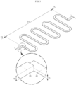
FIG. 2 is a schematic perspective view showing a configuration of a film-type cable according to an embodiment of the present disclosure. -
FIG. 3 is a schematic diagram showing a configuration of a strand of a conducting wire according to an embodiment of the present disclosure. -
FIG. 4 is a plan view of one region of a film-type cable according to the present disclosure. -
FIG. 5 is a schematic cross-sectional view of a film-type cable taken along line A-A' ofFIG. 4 . -
FIG. 6 is a graph showing a result value for each filling thickness of a smoke-proof coating solution during an overcurrent test of a film-type cable according to an embodiment of the present disclosure. -
FIG. 7 , as a diagram corresponding toFIG. 3 , is a schematic diagram showing a configuration of a strand of a conducting wire of a film-type cable according to another embodiment of the present disclosure. -
FIG. 8 , as a diagram corresponding toFIG. 5 , is a schematic cross-sectional view showing a film-type cable according to another embodiment of the present disclosure. - Hereinafter, preferred embodiments of the present disclosure will be described in detail with reference to the accompanying drawings. Prior to the description, it should be understood that the terms used in the specification and the appended claims should not be construed as limited to general and dictionary meanings, but interpreted based on the meanings and concepts corresponding to technical aspects of the present disclosure on the basis of the principle that the inventor is allowed to define terms appropriately for the best explanation. Therefore, the description proposed herein is just a preferable example for the purpose of illustrations only, not intended to limit the scope of the disclosure, so it should be understood that other equivalents and modifications could be made thereto without departing from the scope of the disclosure.
- A film-type cable to be described hereinafter may be interpreted to collectively refer to a flexible flat cable (FFC) or a flexible printed circuit board (FPCB).
- The film-type cable may be used to sense the voltages or temperatures of battery cells and transmit the sensed voltages or temperatures to a battery management system (BMS). Although not shown for convenience of drawings, a cable connector may be coupled to one end of the film-type cable, and welding plates for connecting electrode leads of battery cells to respective conducting wires may be coupled to the other end thereof.
- Although described below in detail, when supplying power or transmitting a signal, a film-type cable according to the present disclosure is configured to block overcurrent by performing a fuse function by itself to prevent the overcurrent from flowing through to a load or the BMS.
-
FIG. 2 is a schematic perspective view showing a configuration of a film-type cable according to an embodiment of the present disclosure, andFIG. 3 is a schematic diagram showing a configuration of a strand of a conducting wire according to an embodiment of the present disclosure. - Referring to the drawings, a film-type cable according to an embodiment of the present disclosure includes an
insulating film 10 and a plurality of conductingwires 20 extending side by side at a predetermined interval and covered with theinsulating film 10. Also, each of the plurality of conductingwires 20 includes afuse pattern section 21 and anormal section 23. - The
insulating film 10 includes abase film 11 and acover film 12 as components for insulating and covering the conductingwires 20. Thebase film 11 is arranged under the plurality of conductingwires 20, and thecover film 12 may be arranged on the plurality of conductingwires 20. - The
insulating film 10 may be manufactured of polyethylen terephthalate (PET), polycyclohexanedimethylene terephthalate (PCT), polyethylene naphthalate (PEN), polyimide (PI), or the like. Preferably, theinsulating film 10 may be manufactured of PI. Among the above-described materials, a PI film has the highest heat resistance, and thus, there is almost no problem even when the PI film is used in a high-temperature environment. - Generally, an FFC is manufactured by attaching conducting wires, which are obtained by processing a thin copper foil plate to a certain width and thickness, onto a base film at a certain interval and attaching again a cover film thereonto. Also, a FPCB is manufactured by arranging a thin copper stack plate on a base film, laminating a dry film, forming conducting wires having a certain interval through exposure, development, and etching processes, and then attaching a cover film thereto. However, the width of a thin copper foil plate may be implemented relatively freely, but it may be difficult to achieve a thickness (height) of a small size of up to units of micrometers (µm), and it may be more difficult to implement a strand of a conducting wire to have various thicknesses. For these reasons, in a method of manufacturing a film-type cable of the related art, it is difficult to implement a fuse pattern on a conducting wire itself.
- Accordingly, instead of the method of manufacturing the film-type cable of the related art, in the film-type cable according to an embodiment of the present disclosure, a printed electronic method is used for manufacturing the plurality of conducting
wires 20. - For example, the plurality of conducting
wires 20 may be implemented by printing silver (Ag) nano electronic ink on a surface of thebase film 11 by using printed electronic equipment. The Ag nano electronic ink printed on thebase film 11 may sufficiently function as aconducting wire 20 having excellent electrical conductivity after a short drying time. Also, according to the printed electronic method, the width of a strand of oneconducting wire 20 may be freely implemented, and various thicknesses thereof may be simply implemented. - That is, in the plurality of conducting
wires 20 of the film-type cable according to an embodiment of the present disclosure, thefuse pattern section 21 and thenormal section 23 may be formed of Ag nano electronic ink. - The
fuse pattern section 21 refers to a section configured to be fused when a current exceeding a rated current flows, and thenormal section 23 refers to a section that is not fused or disconnected when a current exceeding the rated current flows. - In detail, referring to
FIG. 3 , a thickness T1 of theconducting wire 20 in thefuse pattern section 21 is less than a thickness T2 of a conducting wire in thenormal section 23, and theconducting wire 20 is provided to be elongated in thefuse pattern section 21. - For example, when it is assumed that an overcurrent flows in a conducting wire including a portion having a large resistance and a portion having a smaller resistance than that, more heat is generated in the portion having a large resistance. According to (P = I2×R), when an overcurrent flows in the conducting wire, fusion and disconnection are more likely to occur in the portion having a large resistance.
R ≒ L/A [Ω] (R: resistance, L: length of conducting wire, A: cross-sectional area of conducting wire) - As it may be seen from the above formula, the resistance of a conducting wire is proportional to the length of the conducting wire and inversely proportional to the cross-sectional area (through which electric charges pass) thereof, and thus, when a specific portion of the conducting wire is made to be thin and long, the amount of heat generated increases when an overcurrent flows in the corresponding portion, thereby allowing the corresponding portion to act like a fuse.
- The
fuse pattern section 21 of the present embodiment may be said to be designed based on the above principle. That is, the width of theconducting wire 20 is maintained the same by adjusting a printing amount of Ag nano ink in thefuse pattern section 21 and thenormal section 23, but the thickness of theconducting wire 20 is smaller in thefuse pattern section 21 than in thenormal section 23 to reduce the cross-sectional area of theconducting wire 20. For reference, the thickness of theconducting wire 20 in thefuse pattern section 21 may be variously implemented according to the magnitude of rated current that thefuse pattern section 21 may withstand. - In the present embodiment, although the width of the
conducting wire 20 is intactly maintained throughout thefuse pattern section 21 and thenormal section 23 and only the thickness thereof is reduced in thefuse pattern section 21, the width and thickness of theconducting wire 20 may be simultaneously reduced in thefuse pattern section 21. However, in the present embodiment, it is considered that when the width and thickness of theconducting wire 20 are simultaneously reduced, the rigidity of theconducting wire 20 may be significantly reduced. This is to prevent theconducting wire 20 of thefuse pattern section 21 from being easily broken by a physical shock or vibration rather than an overcurrent. - Also, the
conducting wire 20 of the present embodiment may have a repeating "" shape or "S" shape pattern so as to have the length as long as possible within thefuse pattern section 21. - With this configuration, resistance is increased and heat is intensively generated in a region of the
fuse pattern section 21 when an overcurrent occurs, so that thefuse pattern section 21 may be more effectively cut. - Referring back to
FIG. 2 , thefuse pattern sections 21 of neighboring conductingwires 20 may be alternately arranged. - Different magnitudes of current may flow in conducting
wires 20 of the film-type cable, and for example, whenfuse pattern sections 21 ofrespective conducting wires 20 are adjacent to each other (in an X-axis direction), an overcurrent flows in one of the conductingwires 20 such that sparks and heat generated in afuse pattern section 21 of thecorresponding conducting wire 20 may be easily transferred to afuse pattern section 21 of aneighboring conducting wire 20. Accordingly, other surroundingfuse pattern sections 21 may be abnormally fused and disconnected or may emit smoke and ignite. - However, as in the present embodiment, in a case where
fuse pattern sections 21 are alternately arranged, even when sparks or heat are generated in afuse pattern section 21 of oneconducting wire 20, the effect may be small on afuse pattern section 21 ofother conducting wire 20. - Also, the
fuse pattern section 21 of the present embodiment occupies a large area in a width direction (±X direction) of the film-type cable as theconducting wire 20 is formed in a repeating "" shape or "S" shape pattern to extend the length of theconducting wire 20. - In order to arrange the
fuse pattern sections 21 of the conductingwires 20 adjacent to each other (X-axis direction), an interval between conductingwires 20 needs to be increased compared to that of the present embodiment to ensure insulation between the conductingwires 20. Accordingly, an increase in the width of the film-type cable and an increase in a surplus space may be undesirable. - However, in the present embodiment, because the
fuse pattern sections 21 of conductingwires 20 are alternately arranged, ensuring insulation of the conductingwires 20 and setting a minimum pitch thereof may be facilitated. - Meanwhile, the film-type cable according to an embodiment of the present disclosure may further include a smoke-
proof coating solution 40 coated on thefuse pattern section 21 of the plurality of conductingwires 20. - The smoke-
proof coating solution 40 is a component applied to thefuse pattern section 21 to prevent sparks and smoke or scattering of debris during an operation, that is, when theconducting wire 20 is fused and disconnected due to overcurrent. At least one of a urethane resin, an epoxy resin, an epoxy resin, and an acrylic resin may be employed as a material for the smoke-proof coating solution 40. Preferably, polyurethane, which is known as the most effective insulation material while containing relatively few environmentally harmful substances, may be suitable as a material for the smoke-proof coating solution 40. - In detail, referring to
FIGS. 4 and5 , because the conductingwires 20 are formed by printing Ag nano ink on thebase film 11 by the printed electronic method, an adhesive is not required between the conductingwires 20 and thebase film 11, and because an adhesive is used only when thecover film 12 is laminated on the conductingwires 20, anadhesive layer 30 may be provided on the conductingwires 20 in thenormal section 23 and on thecover film 12. - In the present embodiment, the
cover film 12 is used to cover only an upper portion of thenormal section 23 of the conductingwires 20, and an upper portion of thefuse pattern section 21 of the conductingwires 20 is covered by the smoke-proof coating solution 40. Thecover film 12 may be attached onto the conductingwires 20 while a region corresponding to thefuse pattern section 21 is pre-cut, or may be cut off by a region corresponding to thefuse pattern section 21 while being attached onto the conductingwires 20. - Thus, when the
cover film 12 is attached onto the conductingwires 20 printed on thebase film 11, an upper portion of thefuse pattern section 21 is in an open state, and a concave groove portion O surrounded by thecover film 12, theadhesive layer 30, and thefuse pattern section 21 may be formed. The smoke-proof coating solution 40 may be filled in the concave groove portion O, and when a predetermined period of time elapses, the smoke-proof coating solution 40 may be cured to form a coating layer. - Next, in the film-type cable, a design experiment example of the
fuse pattern section 21 will be described. - 1) Length of
conducting wire 20 of fuse pattern section 21: 30-50 mm - 2) Cross-sectional area (SQ) of conducting
wire 20 of fuse pattern section 21: 0.001-0.003 mm2 - 3) Thicknesses of
base film 11 and cover film 12: 25-50 µm - 4) Filling thickness of urethane-based smoke-proof coating solution 40: 0.05-0.45 mm
- While main data of the
fuse pattern section 21 was adjusted within a range of 1) to 4), a short-circuit break test (50 A @ 63 V), a continuous current test (750 A @ 4 hours), and the like were performed, and as a result, the following results were obtained. - In a case where the
conducting wire 20 of thefuse pattern section 21 had the length of 50 mm and the cross-sectional area (SQ) of 0.028 mm^2, when an overcurrent was applied, the performance was the best and scattering did not occur. - In a PEN & PCT film, as the insulating
film 10, scattering was easily generated after the insulatingfilm 10 was melted during an overcurrent application test & a short-circuit break test, but when a PI film was 25µm to 50 µm thick, debris did not all scatter, and thus, there was no significant difference. Thus, it may be said that employing the PI film of 25 µm is reasonable in terms of a cost. - With respect to scattering and duration of smoke emission of a region of the
fuse pattern section 21 according to a filling thickness of the smoke-proof coating solution 40, as shown inFIG. 6 , there was no scattering when the thickness is 0.3 mm or more, and the duration of smoke emission shows similar aspect when the thickness is 0.35 mm and 0.4 mm. - Based on the experiment result, it is appropriate in terms of functionality and economy to design the length of the
conducting wire 20 of thefuse pattern section 21 to be 50 mm and the cross-sectional area thereof to be 0.028 mm^2, and to use thebase film 11 and thecover film 12, each including a PI material and having the thickness of 25 µm, and the urethane-based smoke-proof coating solution 40, wherein the thickness of a smoke-proof coating layer is 0.35 mm. -
FIG. 7 , as a diagram corresponding toFIG. 3 , is a schematic diagram showing a configuration of a strand of aconducting wire 20 of a film-type cable according to another embodiment of the present disclosure, andFIG. 8 , as a diagram corresponding toFIG. 5 , is a schematic diagram showing a film-type cable according to another embodiment of the present disclosure. - Next, referring to
FIGS. 7 and 8 , a film-type cable according to another embodiment of the present disclosure will be described. - The same reference numerals as in the above-described embodiment denote the same members, and duplicate descriptions of the same members are omitted and differences from the above-described embodiments are mainly described.
- When the present embodiment is compared with the above-described embodiment, there is a difference in a
fuse pattern section 21A and remaining components are substantially the same. Aconducting wire 20A in thefuse pattern section 21A of the present embodiment includes a thin-film portion 22a having a certain thickness and extending straight in one direction andprotrusions 22b that are repeatedly formed to protrude upward at a predetermined interval in an extending direction of the thin-film portion 22a. - That is, the
conducting wire 20A is provided to extend straight in one direction when having the same thickness in thenormal section 23 and thefuse pattern section 21A. Thus, pitch setting between the conductingwires 20 may be further facilitated compared to the above-described embodiment. In the above-described embodiment, theconducting wire 20 of thefuse pattern section 21 has a pattern of a "" shape or "S" shape that is repeated and extended, such that an area occupied by thefuse pattern section 21 is large, and thus, may be easily interfered with by a neighboringconducting wire 20, and in order to avoid interference, it is necessary to sufficiently increase the interval between the conductingwires 20. However, according to the present embodiment, a pitch between conductingwires 20A may be easily set, and thus, is free from the same problems as in the above-described embodiment. - Also, the
fuse pattern section 21A of the present embodiment includes the thin-film portion 22a and theprotrusions 22b, and thus, forms a structure in which the thickness of theconducting wire 20A repeatedly increases, decreases, increases, and decreases. Due to the repetition of thickness variation, a fatigue failure phenomenon may be induced whenever an overcurrent passes through a portion where the thickness decreases, and thus, theconducting wire 20A may be easily broken. - Also, the
fuse pattern section 21A of the present embodiment has an uneven structure in a substantially vertical direction, such that the smoke-proof coating solution 40 and theconducting wire 20A of thefuse pattern section 21A may be in contact with each other over a wide area, and thus, the smoke-proof coating solution 40 may be more firmly coupled to thefuse pattern section 21A when cured. - As described above, according to the configuration and operation of the film-type cable according the present disclosure, without mounting a surface-mount device (SMD) fuse on the
conducting wire 20, a fuse function may be implemented. Thus, compared to a film-type cable of the related art, the burden caused by an increase in price due to a material cost of an SMD fuse, a processing cost incurred by mounting the SMD fuse, a defect cost, and the like may be eliminated. - Meanwhile, a battery module according to the present disclosure may include, for example, one or more film-type cables as a component for transmitting a voltage value or temperature value of battery cells to a BMS. Also, the battery module according to the present disclosure may further include, in addition to the film-type cable, a module housing for accommodating battery cells, and various devices for controlling charging/discharging of each of the battery cells, for example, a master BMS, a current sensor, and a fuse.
- The battery module according to the present disclosure may be applied to an electric vehicle, a hybrid vehicle, an energy storage device, and the like.
- As described above, although the present disclosure has been described according to limited embodiments and drawings, the present disclosure is not limited thereto, and various modifications and variations are possible within the scope of the technical idea of the present disclosure and claims to be described below by those of ordinary skill in the art to which the present disclosure pertains.
- Meanwhile, when terms indicating directions such as up, down, left, right, front, and back are used in the present specification, these terms indicate relative positions and are only for convenience of explanation, it is apparent to those skilled in the art that these terms may vary depending on positions of an object, positions of an observer, or the like.
Claims (10)
- A film-type cable comprising:an insulating film; and a plurality of conducting wires covered by the insulating film and extending at a predetermined interval therebetween,wherein each of the plurality of conducting wires comprises:a fuse pattern section provided to be broken when a current exceeding a rated current flows; and a normal section provided not to be broken when a current exceeding the rated current flows, andthe fuse pattern section is thinner than the normal section.
- The film-type cable of claim 1, wherein the insulating film comprises:a base film arranged below the plurality of conducting wires; and a cover film arranged above the plurality of conducting wires in the normal section, andthe plurality of conducting wires are formed of silver nano ink printed on a surface of the base film.
- The film-type cable of claim 2, further comprising a smoke-proof coating solution coated in an upper portion of the fuse pattern section of the plurality of conducting wires.
- The film-type cable of claim 3, wherein an adhesive layer is provided between the plurality of conducting wires in the normal section and the cover film, and
the smoke-proof coating solution is filled in a concave groove portion formed by the cover film, the adhesive layer, and the fuse pattern section. - The film-type cable of claim 3, wherein the smoke-proof coating solution comprises one of a urethane resin, an epoxy resin, and an acrylic resin.
- The film-type cable of claim 1, wherein the fuse pattern sections of the conducting wires adjacent to each other are alternately arranged.
- The film-type cable of claim 1, wherein each of the plurality of conducting wires has the same width in the fuse pattern section as in the normal section and a smaller thickness in the fuse pattern section than in the normal section, and has a pattern of a "" shape or "S" shape that is repeated and extended.

- The film-type cable of claim 1, wherein the conducting wire in the fuse pattern section comprises:
a thin-film portion having a width identical to a width of the conducting wire in the normal section and extending straight; and protrusions that are repeatedly formed to protrude upward at a predetermined interval in an extending direction of the thin-film portion. - The film-type cable of claim 1, wherein the insulating film comprises a polyimide material.
- A battery module comprising the film-type cable according to any one of claims 1 to 9.
Applications Claiming Priority (2)
| Application Number | Priority Date | Filing Date | Title |
|---|---|---|---|
| KR1020200114925A KR102721176B1 (en) | 2020-09-08 | 2020-09-08 | A film type cable with fuse line |
| PCT/KR2021/011882 WO2022055179A1 (en) | 2020-09-08 | 2021-09-02 | Film type cable having fuse line |
Publications (3)
| Publication Number | Publication Date |
|---|---|
| EP4167252A1 true EP4167252A1 (en) | 2023-04-19 |
| EP4167252A4 EP4167252A4 (en) | 2023-11-22 |
| EP4167252B1 EP4167252B1 (en) | 2026-04-15 |
Family
ID=80632288
Family Applications (1)
| Application Number | Title | Priority Date | Filing Date |
|---|---|---|---|
| EP21867045.3A Active EP4167252B1 (en) | 2020-09-08 | 2021-09-02 | Film-type including fuse line |
Country Status (6)
| Country | Link |
|---|---|
| US (1) | US12165790B2 (en) |
| EP (1) | EP4167252B1 (en) |
| JP (1) | JP7589925B2 (en) |
| KR (1) | KR102721176B1 (en) |
| CN (1) | CN115867991A (en) |
| WO (1) | WO2022055179A1 (en) |
Families Citing this family (4)
| Publication number | Priority date | Publication date | Assignee | Title |
|---|---|---|---|---|
| KR20220036131A (en) * | 2020-09-15 | 2022-03-22 | 에스케이온 주식회사 | Sensing assembly and battery module |
| JP7501425B2 (en) * | 2021-03-30 | 2024-06-18 | 株式会社オートネットワーク技術研究所 | Fuse element |
| DE102022132190A1 (en) * | 2022-12-05 | 2024-06-06 | Sumida Flexible Connections Gmbh | Multi-core flat cable system and battery module with corresponding flat cable system |
| CN119108773B (en) * | 2024-11-08 | 2025-02-14 | 中创新航科技集团股份有限公司 | FFC assembly and battery pack |
Family Cites Families (28)
| Publication number | Priority date | Publication date | Assignee | Title |
|---|---|---|---|---|
| US5712610C1 (en) * | 1994-08-19 | 2002-06-25 | Sony Chemicals Corp | Protective device |
| JPH0923048A (en) | 1995-07-07 | 1997-01-21 | Yazaki Corp | Method of manufacturing planar circuit body and planar circuit body |
| WO1999062086A2 (en) | 1998-05-22 | 1999-12-02 | Brooks Dennis L | Vehicle fuse extender unit |
| KR100793725B1 (en) | 2001-07-31 | 2008-01-10 | 삼성전자주식회사 | Flexible film cable |
| JP2006318896A (en) | 2005-04-12 | 2006-11-24 | Mitsubishi Materials Corp | Chip type fuse |
| JP4182120B2 (en) | 2005-06-20 | 2008-11-19 | キヤノン株式会社 | Sheet alignment apparatus and image forming apparatus having the same |
| JP4959267B2 (en) | 2006-03-07 | 2012-06-20 | ルネサスエレクトロニクス株式会社 | Method for increasing resistance value of semiconductor device and electric fuse |
| JP4702174B2 (en) | 2006-05-17 | 2011-06-15 | パナソニック株式会社 | Printed circuit board control device |
| JP5116119B2 (en) * | 2007-03-13 | 2013-01-09 | 国立大学法人埼玉大学 | Fuse link and fuse |
| KR100967037B1 (en) | 2007-10-17 | 2010-06-29 | 주식회사 하이닉스반도체 | Fuse box and its formation method |
| KR200453427Y1 (en) | 2009-07-09 | 2011-05-03 | 박영규 | Thin-walled fuse |
| JP5405391B2 (en) | 2010-05-21 | 2014-02-05 | 日本メクトロン株式会社 | Transparent flexible printed wiring board and manufacturing method thereof |
| JP5505142B2 (en) * | 2010-07-06 | 2014-05-28 | 富士通株式会社 | Fuse and manufacturing method thereof |
| JP2016060089A (en) | 2014-09-17 | 2016-04-25 | 大日本印刷株式会社 | Transfer foil including circuit layer and manufacturing method of transfer foil |
| EP3282467B1 (en) * | 2015-04-07 | 2019-10-23 | SOC Corporation | Fuse production method, fuse, circuit board production method and circuit board |
| JP6453720B2 (en) * | 2015-06-24 | 2019-01-16 | 住友電気工業株式会社 | Flexible printed wiring board |
| WO2016208613A1 (en) * | 2015-06-24 | 2016-12-29 | 住友電工プリントサーキット株式会社 | Flexible printed wiring board |
| JP6659253B2 (en) * | 2015-06-24 | 2020-03-04 | 住友電工プリントサーキット株式会社 | Flexible printed wiring board and method of manufacturing flexible printed wiring board |
| JP6507056B2 (en) * | 2015-07-24 | 2019-04-24 | 株式会社オートネットワーク技術研究所 | Battery wiring module |
| US10593502B1 (en) * | 2018-08-21 | 2020-03-17 | Superior Essex International LP | Fusible continuous shields for use in communication cables |
| JP2017204525A (en) * | 2016-05-10 | 2017-11-16 | 住友電工プリントサーキット株式会社 | Flexible printed wiring board and electronic parts |
| JP6707428B2 (en) | 2016-09-16 | 2020-06-10 | デクセリアルズ株式会社 | Fuse element, fuse element, protection element |
| KR20180011747A (en) | 2017-09-21 | 2018-02-02 | 윤희준 | Flexible flat cable |
| US10796873B2 (en) * | 2017-12-15 | 2020-10-06 | Nio Usa, Inc. | Fusible link in battery module voltage sensing circuit |
| KR102152101B1 (en) | 2018-11-02 | 2020-09-07 | 진영글로벌 주식회사 | vehicle automotive devices |
| KR102757688B1 (en) | 2019-01-28 | 2025-01-21 | 삼성에스디아이 주식회사 | Battery Pack |
| KR20200114925A (en) | 2019-03-28 | 2020-10-07 | 김종현 | Apparatus for coding and decoding of qr code |
| CN210378535U (en) | 2019-07-31 | 2020-04-21 | 东莞市康硕电子有限公司 | FFC flexible flat wire with fusing protection function |
-
2020
- 2020-09-08 KR KR1020200114925A patent/KR102721176B1/en active Active
-
2021
- 2021-09-02 WO PCT/KR2021/011882 patent/WO2022055179A1/en not_active Ceased
- 2021-09-02 EP EP21867045.3A patent/EP4167252B1/en active Active
- 2021-09-02 CN CN202180039524.XA patent/CN115867991A/en active Pending
- 2021-09-02 JP JP2022570490A patent/JP7589925B2/en active Active
- 2021-09-02 US US18/004,759 patent/US12165790B2/en active Active
Also Published As
| Publication number | Publication date |
|---|---|
| JP2023527518A (en) | 2023-06-29 |
| WO2022055179A1 (en) | 2022-03-17 |
| EP4167252A4 (en) | 2023-11-22 |
| US12165790B2 (en) | 2024-12-10 |
| JP7589925B2 (en) | 2024-11-26 |
| CN115867991A (en) | 2023-03-28 |
| KR102721176B1 (en) | 2024-10-22 |
| US20230260675A1 (en) | 2023-08-17 |
| EP4167252B1 (en) | 2026-04-15 |
| KR20220032951A (en) | 2022-03-15 |
Similar Documents
| Publication | Publication Date | Title |
|---|---|---|
| US12165790B2 (en) | Film-type cable including fuse line | |
| EP3866251B1 (en) | Battery pack and vehicle | |
| EP2385568B1 (en) | Protection circuit module and rechargeable battery including the same | |
| US10244621B2 (en) | Flex circuit system for a battery assembly of an electrified vehicle | |
| US10796873B2 (en) | Fusible link in battery module voltage sensing circuit | |
| US8497035B2 (en) | Battery cell integrated measurement sensor line and equalization resistor | |
| US9005786B2 (en) | Integrated cell voltage sense line fusing | |
| JP7339252B2 (en) | FLEXIBLE FLAT CABLE WITH PROTECTIVE ELEMENT MOUNTING, BATTERY MODULE AND METHOD FOR MANUFACTURING FLEXIBLE FLAT CABLE WITH PROTECTIVE ELEMENT MOUNTING | |
| US20130202928A1 (en) | Busbar including flexible circuit | |
| WO2020194967A1 (en) | Overcurrent protection element and battery system | |
| US20190245185A1 (en) | Battery wiring module | |
| US12230838B2 (en) | Battery module using non-welding type structure as connection structure of bus bar and voltage sensing member | |
| EP3961792A1 (en) | Battery module and battery pack including same | |
| EP2742554A2 (en) | Busbar including flexible circuit | |
| KR101110981B1 (en) | Power storage device and wiring pattern | |
| KR102839448B1 (en) | Battery module including flexible printed circuit board sensing liquid | |
| KR20220114913A (en) | Battery module with a busbar frame for efficient lay-out of connector and battery pack including the same | |
| EP4092822B1 (en) | Battery pack | |
| KR102847231B1 (en) | Battery apparatus and method of manufacturing the same | |
| US11552344B2 (en) | Flex foil substrate connector for sensing battery voltage and temperature | |
| US20240072350A1 (en) | Battery pack | |
| US20250233278A1 (en) | Conductive module | |
| KR102931322B1 (en) | Battery module including novel sensing structure and battery pack comprising the same | |
| JP2022057666A (en) | battery | |
| KR20260073828A (en) | Protection curcuit module and battery pack |
Legal Events
| Date | Code | Title | Description |
|---|---|---|---|
| STAA | Information on the status of an ep patent application or granted ep patent |
Free format text: STATUS: THE INTERNATIONAL PUBLICATION HAS BEEN MADE |
|
| PUAI | Public reference made under article 153(3) epc to a published international application that has entered the european phase |
Free format text: ORIGINAL CODE: 0009012 |
|
| STAA | Information on the status of an ep patent application or granted ep patent |
Free format text: STATUS: REQUEST FOR EXAMINATION WAS MADE |
|
| 17P | Request for examination filed |
Effective date: 20230111 |
|
| AK | Designated contracting states |
Kind code of ref document: A1 Designated state(s): AL AT BE BG CH CY CZ DE DK EE ES FI FR GB GR HR HU IE IS IT LI LT LU LV MC MK MT NL NO PL PT RO RS SE SI SK SM TR |
|
| A4 | Supplementary search report drawn up and despatched |
Effective date: 20231018 |
|
| RIC1 | Information provided on ipc code assigned before grant |
Ipc: H02J 7/00 20060101ALI20231013BHEP Ipc: H01H 85/02 20060101ALI20231013BHEP Ipc: H01B 7/02 20060101ALI20231013BHEP Ipc: H01B 9/00 20060101ALI20231013BHEP Ipc: H01B 7/29 20060101ALI20231013BHEP Ipc: H01B 7/32 20060101AFI20231013BHEP |
|
| DAV | Request for validation of the european patent (deleted) | ||
| DAX | Request for extension of the european patent (deleted) | ||
| GRAP | Despatch of communication of intention to grant a patent |
Free format text: ORIGINAL CODE: EPIDOSNIGR1 |
|
| STAA | Information on the status of an ep patent application or granted ep patent |
Free format text: STATUS: GRANT OF PATENT IS INTENDED |
|
| INTG | Intention to grant announced |
Effective date: 20251021 |
|
| P01 | Opt-out of the competence of the unified patent court (upc) registered |
Free format text: CASE NUMBER: UPC_APP_0019789_4167252/2025 Effective date: 20251231 |
|
| GRAS | Grant fee paid |
Free format text: ORIGINAL CODE: EPIDOSNIGR3 |
|
| GRAA | (expected) grant |
Free format text: ORIGINAL CODE: 0009210 |
|
| STAA | Information on the status of an ep patent application or granted ep patent |
Free format text: STATUS: THE PATENT HAS BEEN GRANTED |
|
| AK | Designated contracting states |
Kind code of ref document: B1 Designated state(s): AL AT BE BG CH CY CZ DE DK EE ES FI FR GB GR HR HU IE IS IT LI LT LU LV MC MK MT NL NO PL PT RO RS SE SI SK SM TR |
|
| REG | Reference to a national code |
Ref country code: CH Ref legal event code: F10 Free format text: ST27 STATUS EVENT CODE: U-0-0-F10-F00 (AS PROVIDED BY THE NATIONAL OFFICE) Effective date: 20260415 |
|
| REG | Reference to a national code |
Ref country code: DE Ref legal event code: R096 Ref document number: 602021052295 Country of ref document: DE |
|
| REG | Reference to a national code |
Ref country code: CH Ref legal event code: Q17 Free format text: ST27 STATUS EVENT CODE: U-0-0-Q10-Q17 (AS PROVIDED BY THE NATIONAL OFFICE) Effective date: 20260507 |