EP4166922A1 - High precision vpd-dc scan - Google Patents
High precision vpd-dc scan Download PDFInfo
- Publication number
- EP4166922A1 EP4166922A1 EP22190945.0A EP22190945A EP4166922A1 EP 4166922 A1 EP4166922 A1 EP 4166922A1 EP 22190945 A EP22190945 A EP 22190945A EP 4166922 A1 EP4166922 A1 EP 4166922A1
- Authority
- EP
- European Patent Office
- Prior art keywords
- wafer
- pipette
- scan
- camera
- bulge
- Prior art date
- Legal status (The legal status is an assumption and is not a legal conclusion. Google has not performed a legal analysis and makes no representation as to the accuracy of the status listed.)
- Granted
Links
Images


Classifications
-
- G—PHYSICS
- G01—MEASURING; TESTING
- G01N—INVESTIGATING OR ANALYSING MATERIALS BY DETERMINING THEIR CHEMICAL OR PHYSICAL PROPERTIES
- G01N21/00—Investigating or analysing materials by the use of optical means, i.e. using sub-millimetre waves, infrared, visible or ultraviolet light
- G01N21/84—Systems specially adapted for particular applications
- G01N21/88—Investigating the presence of flaws or contamination
- G01N21/95—Investigating the presence of flaws or contamination characterised by the material or shape of the object to be examined
- G01N21/9501—Semiconductor wafers
-
- H—ELECTRICITY
- H10—SEMICONDUCTOR DEVICES; ELECTRIC SOLID-STATE DEVICES NOT OTHERWISE PROVIDED FOR
- H10P—GENERIC PROCESSES OR APPARATUS FOR THE MANUFACTURE OR TREATMENT OF DEVICES COVERED BY CLASS H10
- H10P74/00—Testing or measuring during manufacture or treatment of wafers, substrates or devices
- H10P74/27—Structural arrangements therefor
-
- G—PHYSICS
- G01—MEASURING; TESTING
- G01N—INVESTIGATING OR ANALYSING MATERIALS BY DETERMINING THEIR CHEMICAL OR PHYSICAL PROPERTIES
- G01N1/00—Sampling; Preparing specimens for investigation
- G01N1/02—Devices for withdrawing samples
-
- G—PHYSICS
- G01—MEASURING; TESTING
- G01N—INVESTIGATING OR ANALYSING MATERIALS BY DETERMINING THEIR CHEMICAL OR PHYSICAL PROPERTIES
- G01N1/00—Sampling; Preparing specimens for investigation
- G01N1/28—Preparing specimens for investigation including physical details of (bio-)chemical methods covered elsewhere, e.g. G01N33/50, C12Q
-
- G—PHYSICS
- G01—MEASURING; TESTING
- G01N—INVESTIGATING OR ANALYSING MATERIALS BY DETERMINING THEIR CHEMICAL OR PHYSICAL PROPERTIES
- G01N21/00—Investigating or analysing materials by the use of optical means, i.e. using sub-millimetre waves, infrared, visible or ultraviolet light
- G01N21/84—Systems specially adapted for particular applications
- G01N21/88—Investigating the presence of flaws or contamination
- G01N21/93—Detection standards; Calibrating baseline adjustment, drift correction
-
- G—PHYSICS
- G01—MEASURING; TESTING
- G01N—INVESTIGATING OR ANALYSING MATERIALS BY DETERMINING THEIR CHEMICAL OR PHYSICAL PROPERTIES
- G01N21/00—Investigating or analysing materials by the use of optical means, i.e. using sub-millimetre waves, infrared, visible or ultraviolet light
- G01N21/84—Systems specially adapted for particular applications
- G01N21/88—Investigating the presence of flaws or contamination
- G01N21/94—Investigating contamination, e.g. dust
-
- G—PHYSICS
- G01—MEASURING; TESTING
- G01N—INVESTIGATING OR ANALYSING MATERIALS BY DETERMINING THEIR CHEMICAL OR PHYSICAL PROPERTIES
- G01N35/00—Automatic analysis not limited to methods or materials provided for in any single one of groups G01N1/00 - G01N33/00; Handling materials therefor
- G01N35/10—Devices for transferring samples or any liquids to, in, or from, the analysis apparatus, e.g. suction devices, injection devices
- G01N35/1009—Characterised by arrangements for controlling the aspiration or dispense of liquids
- G01N35/1011—Control of the position or alignment of the transfer device
-
- H—ELECTRICITY
- H10—SEMICONDUCTOR DEVICES; ELECTRIC SOLID-STATE DEVICES NOT OTHERWISE PROVIDED FOR
- H10P—GENERIC PROCESSES OR APPARATUS FOR THE MANUFACTURE OR TREATMENT OF DEVICES COVERED BY CLASS H10
- H10P72/00—Handling or holding of wafers, substrates or devices during manufacture or treatment thereof
- H10P72/04—Apparatus for manufacture or treatment
- H10P72/0402—Apparatus for fluid treatment
- H10P72/0406—Apparatus for fluid treatment for cleaning followed by drying, rinsing, stripping, blasting or the like
- H10P72/0411—Apparatus for fluid treatment for cleaning followed by drying, rinsing, stripping, blasting or the like for wet cleaning or washing
- H10P72/0414—Apparatus for fluid treatment for cleaning followed by drying, rinsing, stripping, blasting or the like for wet cleaning or washing using mainly spraying means, e.g. nozzles
-
- H—ELECTRICITY
- H10—SEMICONDUCTOR DEVICES; ELECTRIC SOLID-STATE DEVICES NOT OTHERWISE PROVIDED FOR
- H10P—GENERIC PROCESSES OR APPARATUS FOR THE MANUFACTURE OR TREATMENT OF DEVICES COVERED BY CLASS H10
- H10P72/00—Handling or holding of wafers, substrates or devices during manufacture or treatment thereof
- H10P72/04—Apparatus for manufacture or treatment
- H10P72/0402—Apparatus for fluid treatment
- H10P72/0418—Apparatus for fluid treatment for etching
- H10P72/0422—Apparatus for fluid treatment for etching for wet etching
- H10P72/0424—Apparatus for fluid treatment for etching for wet etching using mainly spraying means, e.g. nozzles
-
- H—ELECTRICITY
- H10—SEMICONDUCTOR DEVICES; ELECTRIC SOLID-STATE DEVICES NOT OTHERWISE PROVIDED FOR
- H10P—GENERIC PROCESSES OR APPARATUS FOR THE MANUFACTURE OR TREATMENT OF DEVICES COVERED BY CLASS H10
- H10P72/00—Handling or holding of wafers, substrates or devices during manufacture or treatment thereof
- H10P72/06—Apparatus for monitoring, sorting, marking, testing or measuring
- H10P72/0616—Monitoring of warpages, curvatures, damages, defects or the like
-
- H—ELECTRICITY
- H10—SEMICONDUCTOR DEVICES; ELECTRIC SOLID-STATE DEVICES NOT OTHERWISE PROVIDED FOR
- H10P—GENERIC PROCESSES OR APPARATUS FOR THE MANUFACTURE OR TREATMENT OF DEVICES COVERED BY CLASS H10
- H10P74/00—Testing or measuring during manufacture or treatment of wafers, substrates or devices
- H10P74/20—Testing or measuring during manufacture or treatment of wafers, substrates or devices characterised by the properties tested or measured, e.g. structural or electrical properties
-
- G—PHYSICS
- G01—MEASURING; TESTING
- G01N—INVESTIGATING OR ANALYSING MATERIALS BY DETERMINING THEIR CHEMICAL OR PHYSICAL PROPERTIES
- G01N1/00—Sampling; Preparing specimens for investigation
- G01N1/02—Devices for withdrawing samples
- G01N2001/028—Sampling from a surface, swabbing, vaporising
-
- G—PHYSICS
- G01—MEASURING; TESTING
- G01N—INVESTIGATING OR ANALYSING MATERIALS BY DETERMINING THEIR CHEMICAL OR PHYSICAL PROPERTIES
- G01N21/00—Investigating or analysing materials by the use of optical means, i.e. using sub-millimetre waves, infrared, visible or ultraviolet light
- G01N21/84—Systems specially adapted for particular applications
- G01N21/88—Investigating the presence of flaws or contamination
- G01N21/95—Investigating the presence of flaws or contamination characterised by the material or shape of the object to be examined
- G01N2021/9511—Optical elements other than lenses, e.g. mirrors
-
- G—PHYSICS
- G01—MEASURING; TESTING
- G01N—INVESTIGATING OR ANALYSING MATERIALS BY DETERMINING THEIR CHEMICAL OR PHYSICAL PROPERTIES
- G01N2201/00—Features of devices classified in G01N21/00
- G01N2201/10—Scanning
Definitions
- the invention relates generally to wafer processing and, more specifically, to the analysis of impurities in wafers.
- VPD-DC vapour phase decomposition-droplet collection
- a VPD-DC the surface oxide of a wafer is etched in an HF (hydrogen fluoride) gas atmosphere. Subsequently a small liquid droplet is scanned over the wafer surface to collect and pre-concentrate surface impurities within the droplet.
- Wet chemical analysis by means of, for example, inductively coupled plasma mass spectrometry (ICPMS) or atomic absorption spectroscopy (AAS) can be performed on this sample.
- the droplet can be dried for dry sample analysis like total reflection X-ray fluorescence analysis (TXRF).
- the process module for scanning usually comprises a rotating wafer stage, or scan table, a pipette for droplet deposition, and a scan tube for taking the droplet and guiding it over the wafer surface.
- the pipette deposits a droplet of scanning liquid on the wafer surface.
- the scan tube then takes up the droplet and guides it over the wafer surface as appropriate, e.g. in a spiral trace or in a trace to cover only rings of the surface.
- the pipette again sucks up the scanning liquid, then loaded with the solutes, and transfers it for further analysis.
- VPD-DC VPD-DC
- bevel scan the scanning liquid is guided only along the wafer edge/bevel in a circular trace.
- the droplet is not deposited on the wafer surface, but on a droplet holder, essentially in the form of a small concave plateau, which is placed under the circumferential edge line of the wafer.
- the droplet is then fixed between the scan tube and the droplet holder and the wafer edge touches the fixed droplet from the side while the wafer is rotated on the scan table.
- the present invention aims to provide a system and method that allows scanning very precise and confined bands and areas.
- the invention relates to a method of performing VPD-DC on wafer surfaces, comprising the steps of: a) placing an etched wafer on a rotatable scan table; b) positioning a pipette and the wafer relative to each other such that the pipette tip is in close proximity, but not in contact with the wafer surface; c) operating the pipette such that a bulge of scanning liquid protrudes from the pipette channel and contacts the wafer surface; and d) rotating the wafer to guide the scanning liquid bulge protruding from the pipette channel along the wafer surface.
- the invention does not deposit a droplet of scanning liquid in the wafer surface, or a droplet holder in the case of a bevel scan, and does not use a scan tube to guide the drop across the water surface or along the wafer edge. It rather relies on only a liquid bulge protruding from but never leaving the pipette tip, and not deposited on the wafer surface or a droplet holder. A separate scan rod is not necessary as the pipette assumes its function.
- the present invention also makes it possible to use much smaller liquid volumes for analysis as in previous droplet-based methods, because there is no inherent lower limit to the liquid volume imposed by the droplet.
- the wafers can be silicon wafers, but the invention is also applicable to any other type of wafer.
- the scanning liquid for VPD-DC in general is typically an aqueous solution of HF and H 2 O 2 .
- the method is a bevel scan VPD-DC.
- the pipette and the wafer are positioned relative to each other such that the pipette tip is in close proximity, but not in contact with the wafer bevel.
- the wafer is rotated to guide the scanning liquid bulge protruding from the pipette channel along the wafer bevel.
- the pipette tip is bevelled to create an angled pipette channel opening.
- the angle can correspond approximately to the angle of the wafer bevel. This leads to an improved wetting of the wafer bevel within the inventive concept.
- the pipette tip will preferably be even.
- the method can comprise, in addition to a coarse centering of the wafer on the scan table using a line-scan camera, an advanced centering using a camera with high sensitivity, which allows determination of the position of the wafer edge in xy plane or the pipette tip in xz plane with an accuracy of smaller 10 ⁇ m, preferably smaller 8 ⁇ m, or even smaller 5 ⁇ m.
- the high sensitivity camera is preferably a 2D camera.
- the method can also make use of such high sensitivity camera to fine-tune the relative positions of the pipette tip and the wafer edge / bevel. For any fine tuning changes of relative positions, using the shuttle system of the scan table can be preferred over using robot arms due to the higher achievable precision in movement.
- the bulge contour can be monitored with the high sensitivity camera.
- the pictures can be analysed to determine the success rate of the scan, for example whether there was a tear in the film forming between the bulge and the wafer surface.
- the pictures also convey information whether the volume of the bulge changed during the scan.
- the method can comprise an ongoing adaption of the relative positions of the scan table and the pipette during the scan, based on pre-recorded pictures from the high sensitivity camera.
- the ongoing adaption likewise, using the shuttle system of the scan table is preferred.
- the volume of the bulge is adjusted during the scan to account for an assumed volume decrease of the liquid bulge due to evaporation, or an assumed volume increase of the bulge due to humidity pickup.
- the volume of the bulge can also be adjusted on the basis of information extracted from the picture during the scan to account for an actual volume decrease or increase of the bulge.
- the invention further relates to a system for performing VPD-DC on wafer surfaces, the system comprising a scanning module, the scanning module comprising: a rotable scan table for placing an etched wafer thereon; a pipette for bringing a scanning liquid into contact with the bevel of a wafer placed on the scan table; and a control unit configured to operate the scan table and the pipette such as to carry out a method of the invention.
- the system may further comprise an etching module and, optionally, a drying module.
- the system further comprises a cassette station.
- a robot for wafer transfer can be shared between the modules, or the system can comprise two or more robots (or robot arms).
- the system can also comprise means for wet probe analysis, like inductively coupled plasma mass spectrometry (ICPMS) or atomic absorption spectroscopy (AAS), or dry probe analysis, like total reflection X-ray fluorescence analysis (TXRF).
- ICPMS inductively coupled plasma mass spectrometry
- AAS atomic absorption spectroscopy
- TXRF total reflection X-ray fluorescence analysis
- the system is preferably fully automated and comprises a common control unit, operatively connected to all parts of the system.
- the scan table is usually associated with a shuttle for movement of the scan table in a horizontal plane.
- the system usually comprises a robot for manipulating the pipette and moving it either three-dimensionally or in a plane having a vertical component.
- the pipette tip is bevelled to create an angled pipette channel opening, while in different embodiments, the pipette tip can be even.
- the system can comprise a high precision camera, preferably a 2D camera, which allows determination of the position of the wafer edge in xy plane or the pipette tip in xz plane with an accuracy of smaller 10 ⁇ m, preferably smaller 8 ⁇ m, or even smaller 5 ⁇ m.
- the view direction of the camera is preferably horizontal and along a tangential line of the wafer when in scan position.
- the system may further comprise a droplet holder, preferably in the form of a small concave plateau.
- the droplet holder may be positioned under the circumferential edge line of the wafer and/or below the pipette tip, when in scan position. It can serve to hold a volume of scanning liquid before the liquid is sucked in by the pipette for purposes of the scan, and collect scanning liquid after the scan.
- Figure 1 illustrates a cut view on the edge portion of a wafer 100, where the bevel extending between points A and B and having a width of x, usually around 1 mm, can be recognized.
- the method comprises a step of gross wafer centering on the scan table.
- this step comprises rotating the scan table with the wafer loaded thereon and taking pictures of the wafer edge using a line-scan camera.
- the system is configured such that a picture is taken every 90° of wafer rotation.
- the deviations between the wafer edge positions of the four pictures are used to calculate a better position for the wafer on the scan table.
- a robot lifts the wafer and corrects the deviation in x and y direction. The result is controlled again by the line camera and the process repeated if necessary.
- the gross wafer centering step is completed. There can also be a maximum of iterations, e.g. four iterations, before the step is aborted.
- the gross positioning is followed by a fine positioning using a 2D camera with very good resolution of below 70 ⁇ m, whose view direction is approximately horizontally and along a tangential line of the wafer.
- the fine positioning step comprises moving the scan table and the wafer to a so-called bevel position, using a scan table shuttle operating in xy-plane. In the bevel position, the wafer edge is positioned above a droplet holder.
- the 2D camera then starts capturing a picture of the wafer edge and the wafer rotates for 450°. The captured pictures are analysed to calculate an improved position of the wafer on the scan table.
- the implementation can essentially be as described in connection with the foregoing step, with the only difference that the target deviation is 80 ⁇ m.
- the fine positioning is followed by a step of notch positioning, which includes rotating the scan table until the 2D camera finds the notch of the wafer (which is prefabricated into the wafer before the bevel scanning VPD-DC of the invention is performed). Once the notch position is identified, the scan table is rotated until the notch moves to a predefined (angular) start position.
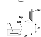
- FIG. 2 shows a side view, as viewed from the perspective of the 2D camera, of the tip 125 of the pipette 120 and the bevel 104 of the wafer 100 during this step.
- the wafer 100 and the pipette 120 are moved to defined raw positions approximating bevel position (wafer) and operative position (pipette).
- the system comprises a robot arm.
- the 2D camera is then used to capture the actual relative positions of the wafer bevel 104 and the pipette tip 125.
- the system calculates the distance between wafer bevel 104 and pipette tip 125 in x and z direction. It then compares this measured distance with a defined distance between the pipette tip 125 and wafer bevel 104 in x and z direction. The deviation is converted into motor steps and feedback is given to the motor of the pipette robot arm and the scan table shuttle. The arm and the scan table shuttle, in response to this information, moves in defined directions to approximate the position required. The camera then captures a picture again, which is evaluated again to confirm that there is an appropriate distance between the pipette tip 125 and the wafer bevel 104 in x and z direction. If the position is not yet appropriate, the process is repeated. If appropriate, the pictures is stored as a reference for the position of wafer 100 and pipette 120 during the subsequent scan.
- the pipette 120 is used to transfer a predefined amount of fresh scanning liquid, e.g. 50-200 ⁇ l, to the droplet holder. It then carries out a rinsing and calibration routine, sucks in the liquid again, and spits back a smaller part of the liquid to avoid any problems resulting from backlash due to a direction change. The pipette 120 is then moved to the defined scan position.
- a predefined amount of fresh scanning liquid e.g. 50-200 ⁇ l
- a small liquid volume of e.g. in the magnitude of 1 ⁇ l is forced out of the pipette tip 120 such that a small bulge 130 of scanning liquid protrudes from the pipette channel and contacts the wafer surface.
- Figure 3 shows a side view of the pipette tip 125 with the protruding bulge 130 of scanning liquid touching the wafer bevel 104 during this step.
- the wafer 100 then rotates for a little under 360°, like 355°, to avoid scanning the notch.
- the scan table moves back to default position and the pipette 120 spits out the entire amount liquid contained in the pipette on the droplet holder.
- the volume of the bulge is adjusted during the scan to account for an assumed volume decrease of the liquid bulge due to evaporation, or an assumed volume increase of the bulge due to humidity pickup. For example, an additional volume in the magnitude of 20% of the initial bulge volume can be added every 90° of the scan.
- the addition or reduction of bulge volume can follow a predetermined scheme, that can be default or based on previous experimentation in a given environment.
- the bulge contour, or length of the partial droplet protruding from the pipette channel can be monitored with the 2D camera.
- the pictures can be analysed to determine the success rate of the scan, for example whether there was a tear in the film connecting the bulge to the wafer surface.
- the length of the bulge reaching from the pipette channel to the wafer surface / bevel in one embodiment, should preferably remain in the range of 1 mm ⁇ 1 ⁇ m.
- the pictures also convey information whether the volume of the bulge changed during the scan.
- the monitoring is used to adjust the volume of the bulge on the basis of information extracted from the picture during the scan to account for an actual volume decrease or increase of the bulge.
- the pipette 120 transfers the liquid comprising the dissolved impurities from the droplet holder to a vial.
- the liquid can be diluted with either water or another scanning liquid to, for example, 650 ⁇ m (ratio 1:4), and further processed.
- the wafer 100 can be transferred back to an aggregate or another station.
- the pipette can self-clean and clean the droplet holder with a cleaning solution.
Landscapes
- Physics & Mathematics (AREA)
- Health & Medical Sciences (AREA)
- Life Sciences & Earth Sciences (AREA)
- Chemical & Material Sciences (AREA)
- Analytical Chemistry (AREA)
- Biochemistry (AREA)
- General Health & Medical Sciences (AREA)
- General Physics & Mathematics (AREA)
- Immunology (AREA)
- Pathology (AREA)
- Sampling And Sample Adjustment (AREA)
- Engineering & Computer Science (AREA)
- Manufacturing & Machinery (AREA)
Abstract
Description
- The invention relates generally to wafer processing and, more specifically, to the analysis of impurities in wafers.
- The progress in semiconductor industry puts stringent demands on the purity of wafers, e.g. silicon wafers, with specifications often going beyond the sensitivities going beyond routine analytical techniques. VPD-DC (vapour phase decomposition-droplet collection) is a sample preparation method used for concentrating impurities on wafer surfaces and improve the sensitivity of subsequent analytical methods.
- In a first step of a VPD-DC, the surface oxide of a wafer is etched in an HF (hydrogen fluoride) gas atmosphere. Subsequently a small liquid droplet is scanned over the wafer surface to collect and pre-concentrate surface impurities within the droplet. Wet chemical analysis by means of, for example, inductively coupled plasma mass spectrometry (ICPMS) or atomic absorption spectroscopy (AAS) can be performed on this sample. Alternatively, the droplet can be dried for dry sample analysis like total reflection X-ray fluorescence analysis (TXRF).
- A major improvement in handling this laborious procedure in practice was the development of fully automated systems, which allow performing cassette-to-cassette VPD-DC processing. These systems comprises two or three process modules to accommodate etching, scanning and, optionally, drying, next to a cassette station and a robot module for wafer transfer. The process module for scanning usually comprises a rotating wafer stage, or scan table, a pipette for droplet deposition, and a scan tube for taking the droplet and guiding it over the wafer surface. Once the freshly etched wafer is placed on the scan table, aligned and flat/notch oriented the scanning procedure is started. The pipette deposits a droplet of scanning liquid on the wafer surface. The scan tube then takes up the droplet and guides it over the wafer surface as appropriate, e.g. in a spiral trace or in a trace to cover only rings of the surface.
- After completion of the scan, the pipette again sucks up the scanning liquid, then loaded with the solutes, and transfers it for further analysis.
- In a variant of VPD-DC, called bevel scan, the scanning liquid is guided only along the wafer edge/bevel in a circular trace. In this variant, the droplet is not deposited on the wafer surface, but on a droplet holder, essentially in the form of a small concave plateau, which is placed under the circumferential edge line of the wafer. The droplet is then fixed between the scan tube and the droplet holder and the wafer edge touches the fixed droplet from the side while the wafer is rotated on the scan table.
- Due to an inherent minimum size and deformation ability of the droplets, a precise scan of only thin bands, e.g. only a 1 mm wide band at the upper bevel surface, has so far not been meaningfully possible. The ability for scanning very precise and confined bands and areas, however, has become interesting in some applications.
- The present invention aims to provide a system and method that allows scanning very precise and confined bands and areas.
- Against this background the invention relates to a method of performing VPD-DC on wafer surfaces, comprising the steps of: a) placing an etched wafer on a rotatable scan table; b) positioning a pipette and the wafer relative to each other such that the pipette tip is in close proximity, but not in contact with the wafer surface; c) operating the pipette such that a bulge of scanning liquid protrudes from the pipette channel and contacts the wafer surface; and d) rotating the wafer to guide the scanning liquid bulge protruding from the pipette channel along the wafer surface.
- Hence, in contrast to the prior art, the invention does not deposit a droplet of scanning liquid in the wafer surface, or a droplet holder in the case of a bevel scan, and does not use a scan tube to guide the drop across the water surface or along the wafer edge. It rather relies on only a liquid bulge protruding from but never leaving the pipette tip, and not deposited on the wafer surface or a droplet holder. A separate scan rod is not necessary as the pipette assumes its function.
- The reliance on only a liquid bulge protruding from the pipette tip, in contrast to a full drop, allows a very careful control of the scanned area and the reduction of the minimum width of a band that can be scanned. For example, the method allows to scan very thin, e.g. smaller 2 mm or even smaller 1 mm wide bands at the upper bevel surface of the wafer, which can be desirable in some applications. In some embodiments, the present invention also makes it possible to use much smaller liquid volumes for analysis as in previous droplet-based methods, because there is no inherent lower limit to the liquid volume imposed by the droplet.
- The wafers can be silicon wafers, but the invention is also applicable to any other type of wafer.
- The scanning liquid for VPD-DC in general is typically an aqueous solution of HF and H2O2.
- In one embodiment, the method is a bevel scan VPD-DC. In this embodiment, in step b), the pipette and the wafer are positioned relative to each other such that the pipette tip is in close proximity, but not in contact with the wafer bevel. In step d), the wafer is rotated to guide the scanning liquid bulge protruding from the pipette channel along the wafer bevel.
- Generally, but in particular in the case of a bevel scan VPD-DC, it can be preferred that the pipette tip is bevelled to create an angled pipette channel opening. The angle can correspond approximately to the angle of the wafer bevel. This leads to an improved wetting of the wafer bevel within the inventive concept.
- In other embodiments, especially if a full or partial scan of the flat surface of the wafer is desired, the pipette tip will preferably be even.
- The use of only a bulge protruding from the pipette for the scan process requires very high precision with regard to the relative positioning of the pipette tip and the wafer.
- For that purpose, the method can comprise, in addition to a coarse centering of the wafer on the scan table using a line-scan camera, an advanced centering using a camera with high sensitivity, which allows determination of the position of the wafer edge in xy plane or the pipette tip in xz plane with an accuracy of smaller 10 µm, preferably smaller 8 µm, or even smaller 5 µm. The high sensitivity camera is preferably a 2D camera. The method can also make use of such high sensitivity camera to fine-tune the relative positions of the pipette tip and the wafer edge / bevel. For any fine tuning changes of relative positions, using the shuttle system of the scan table can be preferred over using robot arms due to the higher achievable precision in movement.
- In one embodiment, the bulge contour can be monitored with the high sensitivity camera. The pictures can be analysed to determine the success rate of the scan, for example whether there was a tear in the film forming between the bulge and the wafer surface. Next to indicating whether the scan was successful the pictures also convey information whether the volume of the bulge changed during the scan.
- In addition, because wafers can be imperfect and not ideally circular, to further improve the precision especially in bevel scans, the method can comprise an ongoing adaption of the relative positions of the scan table and the pipette during the scan, based on pre-recorded pictures from the high sensitivity camera. For the ongoing adaption, likewise, using the shuttle system of the scan table is preferred.
- In one embodiment, the volume of the bulge is adjusted during the scan to account for an assumed volume decrease of the liquid bulge due to evaporation, or an assumed volume increase of the bulge due to humidity pickup. In the case of monitoring the bulge contour, as previously described, the volume of the bulge can also be adjusted on the basis of information extracted from the picture during the scan to account for an actual volume decrease or increase of the bulge.
- Against the background initially described, the invention further relates to a system for performing VPD-DC on wafer surfaces, the system comprising a scanning module, the scanning module comprising: a rotable scan table for placing an etched wafer thereon; a pipette for bringing a scanning liquid into contact with the bevel of a wafer placed on the scan table; and a control unit configured to operate the scan table and the pipette such as to carry out a method of the invention.
- Next to the scanning module, the system may further comprise an etching module and, optionally, a drying module. Typically, the system further comprises a cassette station. A robot for wafer transfer can be shared between the modules, or the system can comprise two or more robots (or robot arms). The system can also comprise means for wet probe analysis, like inductively coupled plasma mass spectrometry (ICPMS) or atomic absorption spectroscopy (AAS), or dry probe analysis, like total reflection X-ray fluorescence analysis (TXRF). The system is preferably fully automated and comprises a common control unit, operatively connected to all parts of the system.
- The scan table is usually associated with a shuttle for movement of the scan table in a horizontal plane. Likewise, the system usually comprises a robot for manipulating the pipette and moving it either three-dimensionally or in a plane having a vertical component.
- As already described in connection with the inventive method, it can be preferred in some embodiments that the pipette tip is bevelled to create an angled pipette channel opening, while in different embodiments, the pipette tip can be even.
- In one embodiment, the system can comprise a high precision camera, preferably a 2D camera, which allows determination of the position of the wafer edge in xy plane or the pipette tip in xz plane with an accuracy of smaller 10 µm, preferably smaller 8 µm, or even smaller 5 µm. The view direction of the camera is preferably horizontal and along a tangential line of the wafer when in scan position.
- The system may further comprise a droplet holder, preferably in the form of a small concave plateau. The droplet holder may be positioned under the circumferential edge line of the wafer and/or below the pipette tip, when in scan position. It can serve to hold a volume of scanning liquid before the liquid is sucked in by the pipette for purposes of the scan, and collect scanning liquid after the scan.
- Further details and advantages of the invention are described in the following with reference to a non-limiting example and illustrative figures. The figures show:
- Figure 1:
- an edge of a wafer and a bevel surface to be scanned in a method according to the invention;
- Figure 2:
- a side view of the pipette tip and the wafer edge during positioning; and
- Figure 3:
- a side view of the pipette tip with a protruding bulge of scanning liquid touching the wafer bevel during scan.
- The example shows a high precision upper bevel scan process and system of the invention to detect surface contamination in wafers.
Figure 1 illustrates a cut view on the edge portion of awafer 100, where the bevel extending between points A and B and having a width of x, usually around 1 mm, can be recognized. - Initially, the method comprises a step of gross wafer centering on the scan table. In more detail, this step comprises rotating the scan table with the wafer loaded thereon and taking pictures of the wafer edge using a line-scan camera. The system is configured such that a picture is taken every 90° of wafer rotation. The deviations between the wafer edge positions of the four pictures are used to calculate a better position for the wafer on the scan table. To implement the calculated improved position, a robot lifts the wafer and corrects the deviation in x and y direction. The result is controlled again by the line camera and the process repeated if necessary. Once a target accuracy of smaller 200 µm deviation between the most removed wafer edge positions is detected, the gross wafer centering step is completed. There can also be a maximum of iterations, e.g. four iterations, before the step is aborted.
- The gross positioning is followed by a fine positioning using a 2D camera with very good resolution of below 70 µm, whose view direction is approximately horizontally and along a tangential line of the wafer. The fine positioning step comprises moving the scan table and the wafer to a so-called bevel position, using a scan table shuttle operating in xy-plane. In the bevel position, the wafer edge is positioned above a droplet holder. The 2D camera then starts capturing a picture of the wafer edge and the wafer rotates for 450°. The captured pictures are analysed to calculate an improved position of the wafer on the scan table. The implementation can essentially be as described in connection with the foregoing step, with the only difference that the target deviation is 80 µm.
- The fine positioning is followed by a step of notch positioning, which includes rotating the scan table until the 2D camera finds the notch of the wafer (which is prefabricated into the wafer before the bevel scanning VPD-DC of the invention is performed). Once the notch position is identified, the scan table is rotated until the notch moves to a predefined (angular) start position.
- The bevelled tip (dual) pipette and the wafer are subsequently, in a next step, positioned relative to each other.
Figure 2 shows a side view, as viewed from the perspective of the 2D camera, of thetip 125 of thepipette 120 and thebevel 104 of thewafer 100 during this step. For this purpose, thewafer 100 and thepipette 120 are moved to defined raw positions approximating bevel position (wafer) and operative position (pipette). For handling thepipette 120, the system comprises a robot arm. The 2D camera is then used to capture the actual relative positions of thewafer bevel 104 and thepipette tip 125. Based on the picture, the system calculates the distance betweenwafer bevel 104 andpipette tip 125 in x and z direction. It then compares this measured distance with a defined distance between thepipette tip 125 andwafer bevel 104 in x and z direction. The deviation is converted into motor steps and feedback is given to the motor of the pipette robot arm and the scan table shuttle. The arm and the scan table shuttle, in response to this information, moves in defined directions to approximate the position required. The camera then captures a picture again, which is evaluated again to confirm that there is an appropriate distance between thepipette tip 125 and thewafer bevel 104 in x and z direction. If the position is not yet appropriate, the process is repeated. If appropriate, the pictures is stored as a reference for the position ofwafer 100 andpipette 120 during the subsequent scan. - Next, the
pipette 120 is used to transfer a predefined amount of fresh scanning liquid, e.g. 50-200 µl, to the droplet holder. It then carries out a rinsing and calibration routine, sucks in the liquid again, and spits back a smaller part of the liquid to avoid any problems resulting from backlash due to a direction change. Thepipette 120 is then moved to the defined scan position. - For carrying out the scan process, a small liquid volume of e.g. in the magnitude of 1 µl is forced out of the
pipette tip 120 such that asmall bulge 130 of scanning liquid protrudes from the pipette channel and contacts the wafer surface.Figure 3 shows a side view of thepipette tip 125 with the protrudingbulge 130 of scanning liquid touching thewafer bevel 104 during this step. Thewafer 100 then rotates for a little under 360°, like 355°, to avoid scanning the notch. After the scan, the scan table moves back to default position and thepipette 120 spits out the entire amount liquid contained in the pipette on the droplet holder. - Provision can be made that the volume of the bulge is adjusted during the scan to account for an assumed volume decrease of the liquid bulge due to evaporation, or an assumed volume increase of the bulge due to humidity pickup. For example, an additional volume in the magnitude of 20% of the initial bulge volume can be added every 90° of the scan. The addition or reduction of bulge volume can follow a predetermined scheme, that can be default or based on previous experimentation in a given environment.
- During the scan, the bulge contour, or length of the partial droplet protruding from the pipette channel, can be monitored with the 2D camera. The pictures can be analysed to determine the success rate of the scan, for example whether there was a tear in the film connecting the bulge to the wafer surface. In terms of numbers, the length of the bulge reaching from the pipette channel to the wafer surface / bevel, in one embodiment, should preferably remain in the range of 1 mm ± 1 µm. Next to indicating whether the scan was successful the pictures also convey information whether the volume of the bulge changed during the scan.
- In the given context of monitoring the bulge contour, provision can also be made that the monitoring is used to adjust the volume of the bulge on the basis of information extracted from the picture during the scan to account for an actual volume decrease or increase of the bulge.
- After the scan, the
pipette 120 transfers the liquid comprising the dissolved impurities from the droplet holder to a vial. The liquid can be diluted with either water or another scanning liquid to, for example, 650 µm (ratio 1:4), and further processed. Thewafer 100 can be transferred back to an aggregate or another station. The pipette can self-clean and clean the droplet holder with a cleaning solution.
Claims (10)
- A method of performing VPD-DC on wafer surfaces, comprising the steps of:a) placing an etched wafer on a rotatable scan table;b) positioning a pipette and the wafer relative to each other such that the pipette tip is in close proximity, but not in contact with the wafer surface;c) operating the pipette such that a bulge of scanning liquid protrudes from the pipette channel and contacts the wafer surface; andd) rotating the wafer to guide the scanning liquid bulge protruding from the pipette channel along the wafer surface.
- The method of claim 1, wherein the method is a bevel scan VPD-DC, wherein in step b) the pipette and the wafer are positioned relative to each other such that the pipette tip is in close proximity but not in contact with the wafer bevel, and wherein in step d) the wafer is rotated to guide the scanning liquid bulge protruding from the pipette channel along the wafer bevel.
- The method of any preceding claim, wherein the method comprises centering the wafer on the horizontal scan table using a 2D camera which allows determination of the position of the wafer edge in xy plane with an accuracy of smaller 10 µm, preferably smaller 8 µm.
- The method of claim 2 or 3, wherein the method comprises fine-tuning the relative positions of the pipette tip in xz plane and the wafer bevel in xy plane using a camera, preferably a 2D camera which allows determination of the position of the wafer edge and the pipette tip with an accuracy of smaller 10 µm, preferably smaller 8 µm.
- The method of any preceding claim, wherein the method comprises an ongoing adaption of the position of the scan table during the scan of step d), based on pre-recorded pictures from a camera, preferably a 2D camera which allows determination of the position of the wafer edge with an accuracy of smaller 10 µm, preferably smaller 8 µm.
- The method of any preceding claim, wherein the method comprises monitoring the bulge contour during the scan using a camera, preferably a 2D camera which allows determination of the bulge contour with an accuracy of smaller 10 µm, preferably smaller 8 µm.
- The method of any preceding claim, wherein during the scanning step d) the volume of the bulge is adjusted to account for an assumed or actual volume decrease or increase of the liquid bulge due to evaporation.
- A system for performing VPD-DC on wafer surfaces, the system comprising a scanning module, the scanning module comprising:a rotable scan table for placing an etched wafer thereon;a pipette for bringing a scanning liquid into contact with the bevel of a wafer placed on the scan table; anda control unit configured to operate the scan table and the pipette such as to carry out a method of any preceding claim.
- The system of claim 8, wherein the pipette tip is bevelled to create an angled pipette channel opening.
- The system of claim 8 or 9, further comprising a high precision camera, preferably a 2D camera, which allows determination of the position of the wafer edge in an xy plane or the pipette tip in an xz plane with an accuracy of smaller 10 µm, preferably smaller 8 µm, or even smaller 5 µm.
Applications Claiming Priority (1)
| Application Number | Priority Date | Filing Date | Title |
|---|---|---|---|
| DE102021126728 | 2021-10-14 |
Publications (3)
| Publication Number | Publication Date |
|---|---|
| EP4166922A1 true EP4166922A1 (en) | 2023-04-19 |
| EP4166922B1 EP4166922B1 (en) | 2026-02-25 |
| EP4166922C0 EP4166922C0 (en) | 2026-02-25 |
Family
ID=83318751
Family Applications (1)
| Application Number | Title | Priority Date | Filing Date |
|---|---|---|---|
| EP22190945.0A Active EP4166922B1 (en) | 2021-10-14 | 2022-08-18 | High precision vpd-dc scan |
Country Status (5)
| Country | Link |
|---|---|
| US (1) | US12379327B2 (en) |
| EP (1) | EP4166922B1 (en) |
| KR (1) | KR102846555B1 (en) |
| CN (1) | CN115547865A (en) |
| TW (1) | TWI832365B (en) |
Cited By (1)
| Publication number | Priority date | Publication date | Assignee | Title |
|---|---|---|---|---|
| CN118645743A (en) * | 2024-08-09 | 2024-09-13 | 比亚迪股份有限公司 | Battery casing, battery, battery pack and electrical equipment |
Citations (7)
| Publication number | Priority date | Publication date | Assignee | Title |
|---|---|---|---|---|
| JP2002093872A (en) * | 2000-09-11 | 2002-03-29 | Toshiba Ceramics Co Ltd | Apparatus and method for recovering analysis solution for measuring impurity amount on wafer surface |
| JP2005327996A (en) * | 2004-05-17 | 2005-11-24 | Sigma Meltec Ltd | Test solution collecting apparatus |
| DE112005001550T5 (en) * | 2004-06-28 | 2007-05-16 | Komatsu Denshi Kinzoku K K | Method and device for collecting chemicals from a semiconductor wafer |
| US9196471B1 (en) * | 2012-06-01 | 2015-11-24 | Yen Fui Choo | Scanner for wafers, method for using the scanner, and components of the scanner |
| US20170069515A1 (en) * | 2011-03-21 | 2017-03-09 | Lg Siltron Inc. | Apparatus for measuring impurities on wafer and method of measuring impurities on wafer |
| CN110634762A (en) * | 2019-09-25 | 2019-12-31 | 上海华力集成电路制造有限公司 | ICPMS test method and ICPMS scanning platform |
| CN213546269U (en) * | 2020-12-17 | 2021-06-25 | 西安奕斯伟硅片技术有限公司 | Wafer surface metal ion collection device |
Family Cites Families (7)
| Publication number | Priority date | Publication date | Assignee | Title |
|---|---|---|---|---|
| JP3467589B2 (en) | 1998-07-01 | 2003-11-17 | 東芝セラミックス株式会社 | Droplet supply / collection device for silicon wafer surface analysis |
| KR100383264B1 (en) * | 2001-03-21 | 2003-05-09 | 삼성전자주식회사 | Collection apparatus and method of metal impurities on the semiconductor wafer |
| US7732225B2 (en) | 2006-06-29 | 2010-06-08 | Texas Instruments Incorporated | Method for measuring contamination in liquids at PPQ levels |
| JP6215059B2 (en) * | 2014-01-10 | 2017-10-18 | 株式会社ディスコ | Mark detection method |
| KR20190047216A (en) * | 2017-10-27 | 2019-05-08 | 주식회사 이오테크닉스 | Wafer calibrating Device and Wafer calibrating Method |
| JP7282640B2 (en) * | 2019-09-12 | 2023-05-29 | 株式会社Screenホールディングス | SUBSTRATE PROCESSING APPARATUS AND SUBSTRATE PROCESSING METHOD |
| CN213042885U (en) * | 2020-10-23 | 2021-04-23 | 合肥晶合集成电路股份有限公司 | Wafer surface metal ion collection device |
-
2022
- 2022-08-05 TW TW111129574A patent/TWI832365B/en active
- 2022-08-11 CN CN202210963875.6A patent/CN115547865A/en active Pending
- 2022-08-18 EP EP22190945.0A patent/EP4166922B1/en active Active
- 2022-09-09 US US17/941,032 patent/US12379327B2/en active Active
- 2022-10-13 KR KR1020220131686A patent/KR102846555B1/en active Active
Patent Citations (7)
| Publication number | Priority date | Publication date | Assignee | Title |
|---|---|---|---|---|
| JP2002093872A (en) * | 2000-09-11 | 2002-03-29 | Toshiba Ceramics Co Ltd | Apparatus and method for recovering analysis solution for measuring impurity amount on wafer surface |
| JP2005327996A (en) * | 2004-05-17 | 2005-11-24 | Sigma Meltec Ltd | Test solution collecting apparatus |
| DE112005001550T5 (en) * | 2004-06-28 | 2007-05-16 | Komatsu Denshi Kinzoku K K | Method and device for collecting chemicals from a semiconductor wafer |
| US20170069515A1 (en) * | 2011-03-21 | 2017-03-09 | Lg Siltron Inc. | Apparatus for measuring impurities on wafer and method of measuring impurities on wafer |
| US9196471B1 (en) * | 2012-06-01 | 2015-11-24 | Yen Fui Choo | Scanner for wafers, method for using the scanner, and components of the scanner |
| CN110634762A (en) * | 2019-09-25 | 2019-12-31 | 上海华力集成电路制造有限公司 | ICPMS test method and ICPMS scanning platform |
| CN213546269U (en) * | 2020-12-17 | 2021-06-25 | 西安奕斯伟硅片技术有限公司 | Wafer surface metal ion collection device |
Cited By (1)
| Publication number | Priority date | Publication date | Assignee | Title |
|---|---|---|---|---|
| CN118645743A (en) * | 2024-08-09 | 2024-09-13 | 比亚迪股份有限公司 | Battery casing, battery, battery pack and electrical equipment |
Also Published As
| Publication number | Publication date |
|---|---|
| US12379327B2 (en) | 2025-08-05 |
| EP4166922B1 (en) | 2026-02-25 |
| TW202333254A (en) | 2023-08-16 |
| CN115547865A (en) | 2022-12-30 |
| US20230118379A1 (en) | 2023-04-20 |
| TWI832365B (en) | 2024-02-11 |
| KR20230053535A (en) | 2023-04-21 |
| KR102846555B1 (en) | 2025-08-18 |
| EP4166922C0 (en) | 2026-02-25 |
Similar Documents
| Publication | Publication Date | Title |
|---|---|---|
| KR101878995B1 (en) | Liquid processing apparatus, liquid processing method and storage medium | |
| KR101868775B1 (en) | Silicon substrate analyzing device | |
| KR100278331B1 (en) | Multichamber substrate processing device | |
| JPH02236149A (en) | Printed circuit inspection system | |
| JP6680040B2 (en) | Substrate processing apparatus, liquid processing method, and storage medium | |
| KR20090105584A (en) | GP unit and door opening and closing device of semiconductor wafer pollutant measuring device | |
| US12379327B2 (en) | High precision VPD-DC scan | |
| CN103443911A (en) | Apparatus for measuring impurities on wafer and method of measuring impurities on wafer | |
| CN111415889A (en) | Wafer state detection method and semiconductor device | |
| KR102226471B1 (en) | Method of Sample solution sampling of substrate inspection machine and device therefor | |
| WO2024250765A1 (en) | Three-dimensional laser ablation mass spectrometer, combined detection system, and detection method | |
| JP2006140350A (en) | Substrate processing apparatus and teaching method | |
| CN205786470U (en) | Substrate analytical equipment | |
| JP3784696B2 (en) | Semiconductor wafer surface impurity recovery method and recovery apparatus | |
| US7399635B2 (en) | Impurity measuring method for Ge substrates | |
| US20250385111A1 (en) | Methods and Apparatus for Determining a Property of a Substrate Surface | |
| US20250334445A1 (en) | Substrate measurement systems having substrate holders | |
| TWI920771B (en) | Wafer conveying and measurement system | |
| US20250336711A1 (en) | Substrate holder systems | |
| JP2020106303A (en) | Substrate analysis method and substrate analysis device | |
| KR20250051827A (en) | Contaminant collection device of substrate contaminant analysis equipment | |
| WO2003041159A1 (en) | Wafer observation position designating apparatus, and wafer display position designating method | |
| CN120319673A (en) | A device and method for detecting metal contamination on silicon wafer surface | |
| US20040009619A1 (en) | Automatic fluid scanner | |
| CN119673797A (en) | A method and device for collecting wafer surface material |
Legal Events
| Date | Code | Title | Description |
|---|---|---|---|
| PUAI | Public reference made under article 153(3) epc to a published international application that has entered the european phase |
Free format text: ORIGINAL CODE: 0009012 |
|
| STAA | Information on the status of an ep patent application or granted ep patent |
Free format text: STATUS: REQUEST FOR EXAMINATION WAS MADE |
|
| 17P | Request for examination filed |
Effective date: 20220818 |
|
| AK | Designated contracting states |
Kind code of ref document: A1 Designated state(s): AL AT BE BG CH CY CZ DE DK EE ES FI FR GB GR HR HU IE IS IT LI LT LU LV MC MK MT NL NO PL PT RO RS SE SI SK SM TR |
|
| REG | Reference to a national code |
Ref country code: DE Ref legal event code: R079 Free format text: PREVIOUS MAIN CLASS: G01N0001140000 Ipc: H01L0021670000 Ref country code: DE Ref legal event code: R079 Ref document number: 602022031003 Country of ref document: DE Free format text: PREVIOUS MAIN CLASS: G01N0001140000 Ipc: H01L0021670000 |
|
| GRAP | Despatch of communication of intention to grant a patent |
Free format text: ORIGINAL CODE: EPIDOSNIGR1 |
|
| STAA | Information on the status of an ep patent application or granted ep patent |
Free format text: STATUS: GRANT OF PATENT IS INTENDED |
|
| RIC1 | Information provided on ipc code assigned before grant |
Ipc: H01L 21/67 20060101AFI20250908BHEP Ipc: G01N 1/32 20060101ALI20250908BHEP Ipc: G01N 1/28 20060101ALI20250908BHEP Ipc: G01N 1/14 20060101ALI20250908BHEP Ipc: G01N 1/02 20060101ALN20250908BHEP |
|
| INTG | Intention to grant announced |
Effective date: 20250918 |
|
| GRAS | Grant fee paid |
Free format text: ORIGINAL CODE: EPIDOSNIGR3 |
|
| GRAA | (expected) grant |
Free format text: ORIGINAL CODE: 0009210 |
|
| STAA | Information on the status of an ep patent application or granted ep patent |
Free format text: STATUS: THE PATENT HAS BEEN GRANTED |
|
| AK | Designated contracting states |
Kind code of ref document: B1 Designated state(s): AL AT BE BG CH CY CZ DE DK EE ES FI FR GB GR HR HU IE IS IT LI LT LU LV MC MK MT NL NO PL PT RO RS SE SI SK SM TR |
|
| REG | Reference to a national code |
Ref country code: CH Ref legal event code: F10 Free format text: ST27 STATUS EVENT CODE: U-0-0-F10-F00 (AS PROVIDED BY THE NATIONAL OFFICE) Effective date: 20260225 Ref country code: GB Ref legal event code: FG4D |
|
| REG | Reference to a national code |
Ref country code: IE Ref legal event code: FG4D |
|
| U01 | Request for unitary effect filed |
Effective date: 20260225 |
|
| U07 | Unitary effect registered |
Designated state(s): AT BE BG DE DK EE FI FR IT LT LU LV MT NL PT RO SE SI Effective date: 20260303 |