EP4163985A1 - Semiconductor light-emitting device, and water disinfection device - Google Patents
Semiconductor light-emitting device, and water disinfection device Download PDFInfo
- Publication number
- EP4163985A1 EP4163985A1 EP21822043.2A EP21822043A EP4163985A1 EP 4163985 A1 EP4163985 A1 EP 4163985A1 EP 21822043 A EP21822043 A EP 21822043A EP 4163985 A1 EP4163985 A1 EP 4163985A1
- Authority
- EP
- European Patent Office
- Prior art keywords
- semiconductor light
- emitting device
- bonding pattern
- bonding
- emitting element
- Prior art date
- Legal status (The legal status is an assumption and is not a legal conclusion. Google has not performed a legal analysis and makes no representation as to the accuracy of the status listed.)
- Pending
Links
Images








Classifications
-
- H—ELECTRICITY
- H10—SEMICONDUCTOR DEVICES; ELECTRIC SOLID-STATE DEVICES NOT OTHERWISE PROVIDED FOR
- H10H—INORGANIC LIGHT-EMITTING SEMICONDUCTOR DEVICES HAVING POTENTIAL BARRIERS
- H10H20/00—Individual inorganic light-emitting semiconductor devices having potential barriers, e.g. light-emitting diodes [LED]
- H10H20/80—Constructional details
- H10H20/85—Packages
- H10H20/8506—Containers
-
- A—HUMAN NECESSITIES
- A61—MEDICAL OR VETERINARY SCIENCE; HYGIENE
- A61L—METHODS OR APPARATUS FOR STERILISING MATERIALS OR OBJECTS IN GENERAL; DISINFECTION, STERILISATION OR DEODORISATION OF AIR; CHEMICAL ASPECTS OF BANDAGES, DRESSINGS, ABSORBENT PADS OR SURGICAL ARTICLES; MATERIALS FOR BANDAGES, DRESSINGS, ABSORBENT PADS OR SURGICAL ARTICLES
- A61L2/00—Disinfection or sterilisation of materials or objects, in general; Accessories therefor
- A61L2/02—Disinfection or sterilisation of materials or objects, in general; Accessories therefor using physical processes
- A61L2/08—Radiation
- A61L2/10—Ultraviolet [UV] radiation
-
- C—CHEMISTRY; METALLURGY
- C02—TREATMENT OF WATER, WASTE WATER, SEWAGE, OR SLUDGE
- C02F—TREATMENT OF WATER, WASTE WATER, SEWAGE, OR SLUDGE
- C02F1/00—Treatment of water, waste water, or sewage
- C02F1/30—Treatment of water, waste water, or sewage by irradiation
- C02F1/32—Treatment of water, waste water, or sewage by irradiation with ultraviolet light
- C02F1/325—Irradiation devices or lamp constructions
-
- H—ELECTRICITY
- H01—ELECTRIC ELEMENTS
- H01S—DEVICES USING THE PROCESS OF LIGHT AMPLIFICATION BY STIMULATED EMISSION OF RADIATION [LASER] TO AMPLIFY OR GENERATE LIGHT; DEVICES USING STIMULATED EMISSION OF ELECTROMAGNETIC RADIATION IN WAVE RANGES OTHER THAN OPTICAL
- H01S5/00—Semiconductor lasers
- H01S5/02—Structural details or components not essential to laser action
- H01S5/022—Mountings; Housings
- H01S5/02208—Mountings; Housings characterised by the shape of the housings
-
- H—ELECTRICITY
- H01—ELECTRIC ELEMENTS
- H01S—DEVICES USING THE PROCESS OF LIGHT AMPLIFICATION BY STIMULATED EMISSION OF RADIATION [LASER] TO AMPLIFY OR GENERATE LIGHT; DEVICES USING STIMULATED EMISSION OF ELECTROMAGNETIC RADIATION IN WAVE RANGES OTHER THAN OPTICAL
- H01S5/00—Semiconductor lasers
- H01S5/02—Structural details or components not essential to laser action
- H01S5/022—Mountings; Housings
- H01S5/0225—Out-coupling of light
- H01S5/02253—Out-coupling of light using lenses
-
- H—ELECTRICITY
- H01—ELECTRIC ELEMENTS
- H01S—DEVICES USING THE PROCESS OF LIGHT AMPLIFICATION BY STIMULATED EMISSION OF RADIATION [LASER] TO AMPLIFY OR GENERATE LIGHT; DEVICES USING STIMULATED EMISSION OF ELECTROMAGNETIC RADIATION IN WAVE RANGES OTHER THAN OPTICAL
- H01S5/00—Semiconductor lasers
- H01S5/02—Structural details or components not essential to laser action
- H01S5/022—Mountings; Housings
- H01S5/023—Mount members, e.g. sub-mount members
-
- H—ELECTRICITY
- H01—ELECTRIC ELEMENTS
- H01S—DEVICES USING THE PROCESS OF LIGHT AMPLIFICATION BY STIMULATED EMISSION OF RADIATION [LASER] TO AMPLIFY OR GENERATE LIGHT; DEVICES USING STIMULATED EMISSION OF ELECTROMAGNETIC RADIATION IN WAVE RANGES OTHER THAN OPTICAL
- H01S5/00—Semiconductor lasers
- H01S5/02—Structural details or components not essential to laser action
- H01S5/022—Mountings; Housings
- H01S5/0235—Method for mounting laser chips
- H01S5/02355—Fixing laser chips on mounts
- H01S5/0237—Fixing laser chips on mounts by soldering
-
- H—ELECTRICITY
- H10—SEMICONDUCTOR DEVICES; ELECTRIC SOLID-STATE DEVICES NOT OTHERWISE PROVIDED FOR
- H10H—INORGANIC LIGHT-EMITTING SEMICONDUCTOR DEVICES HAVING POTENTIAL BARRIERS
- H10H20/00—Individual inorganic light-emitting semiconductor devices having potential barriers, e.g. light-emitting diodes [LED]
- H10H20/80—Constructional details
- H10H20/85—Packages
- H10H20/855—Optical field-shaping means, e.g. lenses
-
- C—CHEMISTRY; METALLURGY
- C02—TREATMENT OF WATER, WASTE WATER, SEWAGE, OR SLUDGE
- C02F—TREATMENT OF WATER, WASTE WATER, SEWAGE, OR SLUDGE
- C02F2201/00—Apparatus for treatment of water, waste water or sewage
- C02F2201/32—Details relating to UV-irradiation devices
- C02F2201/322—Lamp arrangement
- C02F2201/3222—Units using UV-light emitting diodes [LED]
-
- C—CHEMISTRY; METALLURGY
- C02—TREATMENT OF WATER, WASTE WATER, SEWAGE, OR SLUDGE
- C02F—TREATMENT OF WATER, WASTE WATER, SEWAGE, OR SLUDGE
- C02F2201/00—Apparatus for treatment of water, waste water or sewage
- C02F2201/32—Details relating to UV-irradiation devices
- C02F2201/322—Lamp arrangement
- C02F2201/3226—Units using UV-light emitting lasers
-
- C—CHEMISTRY; METALLURGY
- C02—TREATMENT OF WATER, WASTE WATER, SEWAGE, OR SLUDGE
- C02F—TREATMENT OF WATER, WASTE WATER, SEWAGE, OR SLUDGE
- C02F2303/00—Specific treatment goals
- C02F2303/04—Disinfection
-
- H—ELECTRICITY
- H01—ELECTRIC ELEMENTS
- H01S—DEVICES USING THE PROCESS OF LIGHT AMPLIFICATION BY STIMULATED EMISSION OF RADIATION [LASER] TO AMPLIFY OR GENERATE LIGHT; DEVICES USING STIMULATED EMISSION OF ELECTROMAGNETIC RADIATION IN WAVE RANGES OTHER THAN OPTICAL
- H01S5/00—Semiconductor lasers
- H01S5/02—Structural details or components not essential to laser action
- H01S5/022—Mountings; Housings
- H01S5/02218—Material of the housings; Filling of the housings
-
- H—ELECTRICITY
- H01—ELECTRIC ELEMENTS
- H01S—DEVICES USING THE PROCESS OF LIGHT AMPLIFICATION BY STIMULATED EMISSION OF RADIATION [LASER] TO AMPLIFY OR GENERATE LIGHT; DEVICES USING STIMULATED EMISSION OF ELECTROMAGNETIC RADIATION IN WAVE RANGES OTHER THAN OPTICAL
- H01S5/00—Semiconductor lasers
- H01S5/02—Structural details or components not essential to laser action
- H01S5/022—Mountings; Housings
- H01S5/02218—Material of the housings; Filling of the housings
- H01S5/0222—Gas-filled housings
-
- H—ELECTRICITY
- H01—ELECTRIC ELEMENTS
- H01S—DEVICES USING THE PROCESS OF LIGHT AMPLIFICATION BY STIMULATED EMISSION OF RADIATION [LASER] TO AMPLIFY OR GENERATE LIGHT; DEVICES USING STIMULATED EMISSION OF ELECTROMAGNETIC RADIATION IN WAVE RANGES OTHER THAN OPTICAL
- H01S5/00—Semiconductor lasers
- H01S5/02—Structural details or components not essential to laser action
- H01S5/022—Mountings; Housings
- H01S5/0225—Out-coupling of light
- H01S5/02257—Out-coupling of light using windows, e.g. specially adapted for back-reflecting light to a detector inside the housing
-
- H—ELECTRICITY
- H01—ELECTRIC ELEMENTS
- H01S—DEVICES USING THE PROCESS OF LIGHT AMPLIFICATION BY STIMULATED EMISSION OF RADIATION [LASER] TO AMPLIFY OR GENERATE LIGHT; DEVICES USING STIMULATED EMISSION OF ELECTROMAGNETIC RADIATION IN WAVE RANGES OTHER THAN OPTICAL
- H01S5/00—Semiconductor lasers
- H01S5/10—Construction or shape of the optical resonator, e.g. extended or external cavity, coupled cavities, bent-guide, varying width, thickness or composition of the active region
- H01S5/18—Surface-emitting [SE] lasers, e.g. having both horizontal and vertical cavities
- H01S5/183—Surface-emitting [SE] lasers, e.g. having both horizontal and vertical cavities having only vertical cavities, e.g. vertical cavity surface-emitting lasers [VCSEL]
-
- H—ELECTRICITY
- H01—ELECTRIC ELEMENTS
- H01S—DEVICES USING THE PROCESS OF LIGHT AMPLIFICATION BY STIMULATED EMISSION OF RADIATION [LASER] TO AMPLIFY OR GENERATE LIGHT; DEVICES USING STIMULATED EMISSION OF ELECTROMAGNETIC RADIATION IN WAVE RANGES OTHER THAN OPTICAL
- H01S5/00—Semiconductor lasers
- H01S5/30—Structure or shape of the active region; Materials used for the active region
- H01S5/32—Structure or shape of the active region; Materials used for the active region comprising PN junctions, e.g. hetero- or double- heterostructures
- H01S5/323—Structure or shape of the active region; Materials used for the active region comprising PN junctions, e.g. hetero- or double- heterostructures in AIIIBV compounds, e.g. AlGaAs-laser, InP-based laser
- H01S5/32308—Structure or shape of the active region; Materials used for the active region comprising PN junctions, e.g. hetero- or double- heterostructures in AIIIBV compounds, e.g. AlGaAs-laser, InP-based laser emitting light at a wavelength less than 900 nm
- H01S5/32341—Structure or shape of the active region; Materials used for the active region comprising PN junctions, e.g. hetero- or double- heterostructures in AIIIBV compounds, e.g. AlGaAs-laser, InP-based laser emitting light at a wavelength less than 900 nm blue laser based on GaN or GaP
-
- H—ELECTRICITY
- H10—SEMICONDUCTOR DEVICES; ELECTRIC SOLID-STATE DEVICES NOT OTHERWISE PROVIDED FOR
- H10H—INORGANIC LIGHT-EMITTING SEMICONDUCTOR DEVICES HAVING POTENTIAL BARRIERS
- H10H20/00—Individual inorganic light-emitting semiconductor devices having potential barriers, e.g. light-emitting diodes [LED]
- H10H20/01—Manufacture or treatment
- H10H20/036—Manufacture or treatment of packages
Definitions
- the present invention relates to a semiconductor light-emitting device in which a space around a semiconductor light-emitting element is sealed airtightly.
- an airtight package in a semiconductor light-emitting device that requires airtightness uses a structure in which a flat plate-shaped translucent optical element is bonded to a cavity-type substrate as disclosed in PTL 1, or a structure in which a cavity-type translucent optical element is bonded to a flat plate-shaped substrate as disclosed in PTL 2.
- an optical element such as glass and a heat dissipation substrate such as a ceramic substrate are bonded to each other and sealed by solder such as AuSn or a brazing material.
- PTL 3 suggests a structure of suppressing protrusion of solder from a bonding pattern by forming a film such as an oxide film that has poor solder wettability in an inner peripheral portion and an outer peripheral portion of a bonding area.
- PTL 4 suggests a structure in which a recessed structure is formed on a substrate and protruding solder is accommodated in a recessed portion to suppress wetting and spreading of the solder outside of the recessed portion.
- An object of the invention is to newly provide a semiconductor light-emitting device having high airtight reliability by increasing bonding reliability between a substrate and a lid.
- a semiconductor light-emitting device includes a substrate; a semiconductor light-emitting element that is mounted on the substrate; and a dome-shaped transparent body that is mounted on the substrate.
- the dome-shaped transparent body includes a convex lid portion that covers a space around the semiconductor light-emitting element and includes an annular base portion and a flange portion that projects to an outer side of an outer peripheral edge of the annular base portion.
- a first bonding pattern made of metal that surrounds the semiconductor light-emitting element is formed on the substrate.
- a second bonding pattern having a shape corresponding to the first bonding pattern is provided in the base portion and the flange portion of the dome-shaped transparent body.
- the first bonding pattern and the second bonding pattern are bonded to each other via solder, to seal the space in the convex lid portion.
- the first bonding pattern and the second bonding pattern have rectangular ring shapes that surround the semiconductor light-emitting element when viewed from above, at least edges on inner peripheral sides of corner portions thereof are positioned on outer sides of outer peripheral edges of the annular base portion of the convex lid portion, and at least edges on inner peripheral sides of straight-line portions sandwiched between the corner portions are positioned closer to the semiconductor light-emitting element than the outer peripheral edge of the annular base portion of the convex lid portion.
- a bonding pattern between a substrate and a dome-shaped transparent body has a rectangular ring shape when viewed from above, corner portions thereof are positioned on outer sides of an annular base portion of a convex lid portion to which a load is applied when a dome-shaped transparent body is pressed at the time of bonding, and thus it is possible to provide a semiconductor light-emitting device in which generation of voids in a bonding portion is suppressed, bonding reliability is high, and airtight reliability is high.
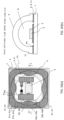
- a configuration of a semiconductor light-emitting device according to Embodiment 1 is described with reference to FIG. 1 to FIG. 7 .
- FIGS. 1(a) and 1(b) A top view and a cross-sectional view of the semiconductor light-emitting device according to Embodiment 1 are illustrated in FIGS. 1(a) and 1(b) .
- the semiconductor light-emitting device includes a substrate 1, a semiconductor light-emitting element 3 mounted on an electrode 2 on the substrate 1, and a dome-shaped transparent body 4 mounted on the substrate 1.
- the dome-shaped transparent body 4 covers a space around the semiconductor light-emitting element 3 and includes a convex lid portion 4a including an annular base portion 4c and a flange portion 4b projecting to an outer side of an outer peripheral edge of the annular base portion 4c.
- the base portion 4c has an annular shape with a predetermined width.
- the base portion 4c is a root portion of the convex lid portion 4a that configures a bottom surface with a thickness of the convex lid portion 4a, in the dome-shaped transparent body 4.
- both the substrate 1 and the flange portion 4b have rectangular shapes when viewed from above, and the dome-shaped transparent body 4 is mounted on the substrate 1 so that directions of corner portions are the same.
- the size of the flange portion 4b is slightly smaller than that of the substrate 1 in the present embodiment.
- the annular base portion 4c and the flange portion 4b of the dome-shaped transparent body 4, and the substrate 1 in contact with the annular base portion 4c and the flange portion 4b are respectively provided with the bonding patterns 5 and 6 having corresponding shapes.
- the bonding patterns 5 and 6 are provided along the rectangular appearances of the flange portion 4b and the substrate 1.
- FIGS. 4(a) and 4(b) A top view and a cross-sectional view of the substrate 1 in which the bonding pattern 6 is provided are illustrated in FIGS. 4(a) and 4(b) .
- a top view and a cross-sectional view of the dome-shaped transparent body 4 in which the bonding pattern 5 is provided are illustrated in FIGS. 5(a) and 5(b) .
- the bonding patterns 5 and 6 are formed with a predetermined width so as to surround the semiconductor light-emitting element 3, and have rectangular ring shapes.
- the bonding pattern 5 provided in the dome-shaped transparent body 4 includes four straight-line portions 52 formed along the sides that configure the outer shape of the dome-shaped transparent body 4 and corner portions 51 that connect between the adjacent straight-line portions 52.
- the bonding pattern 6 provided on the substrate 1 includes four straight-line portions 62 formed along the sides that configure the outer shape of the substrate 1 and corner portions 61 that connect the adjacent straight-line portions 62.
- the bonding patterns 5 and 6 are bonded to each other via the solder 7, to form a bonding layer 7a (see FIG. 3 ). Accordingly, a space 8 in the convex lid portion 4 is sealed.
- the bonding layer 7a wets and spreads along the bonding pattern and has a fillet shape as a whole end portion.
- the terminal end portion may have a slightly raised shape due to the action of surface tension.
- the solder 7 may be in contact with the side surface of the bonding pattern 5.
- the width of the bonding pattern 5 on a transparent body 4 side is preferably narrower than the width of the bonding pattern 6 on a substrate 1 side.
- the corner portions 51 and 61 of the bonding patterns 5 and 6 having the rectangular ring shapes are configured so that edges 51a and 61a on an outer peripheral side are at least positioned on an outer side of an outer peripheral edge 41 of the annular base portion 4c of the convex lid portion 4a (see FIG. 1(a) ).
- edges 51b and 61b on an inner peripheral side of the corner portions 51 and 61 of the bonding patterns 5 and 6 are also preferably positioned on the outer side of the outer peripheral edge 41 of the annular base portion 4c of the convex lid portion 4a.
- the bonding pattern 5 provided in the dome-shaped transparent body 4 is provided so that the straight-line portion 52 partially overlaps with the base portion 4c, and at least a part of the corner portion 51 is provided to be positioned on an outer side of the base portion 4c. That is, an area that does not overlap with the base portion 4c is provided in the corner portion 51.
- edges 52b and 62b on the inner peripheral side are at least positioned on the semiconductor light-emitting element 3 side of the outer peripheral edge 41 of the annular base portion 4c of the convex lid portion 4a (see FIG. 1(a) ).
- edges 52a and 62a on the outer peripheral side of the straight-line portions 52 and 62 of the bonding patterns 5 and 6 with the rectangular ring shape are preferably positioned on the outer side of the outer peripheral edge 41 of the base portion 4c.
- the bonding pattern 6 provided on the substrate 1 is provided so that the straight-line portion 62 partially overlaps with the base portion 4c, and at least a part of the corner portion 61 is provided to be positioned on the outer side of the base portion 4c. That is, an area that does not overlap with the base portion 4c is provided in the corner portion 61.
- the semiconductor light-emitting device uses the bonding patterns 5 and 6 with the rectangular ring shape and is configured so that the corner portions 51 and 61 thereof are positioned on the outer side of the outer peripheral edge 41 of the annular base portion 4c to which a load is most applied, the load being applied to the convex lid portion 4a when the dome-shaped transparent body 4 is bonded.
- the straight-line portions 52 and 62 of the bonding patterns 5 and 6 are configured so that at least a part thereof is positioned under the base portion 4c to which a load is most applied. Accordingly, in the bonding process, the loads applied to the corner portions 51 and 61 of the bonding patterns 5 and 6 are smaller than the loads applied to the straight-line portions 52 and 62.
- the solder 7 disposed between the bonding patterns 5 and 6 starts to melt from an area sandwiched between the straight-line portions 52 and 62 to which a load is most applied (more specifically, an area where the base portion 4c overlaps in a thickness direction).
- the solder 7 in an area sandwiched between the corner portions 51 and 61 is not melted but is melted thereafter. Accordingly, as illustrated in FIG.
- the melting direction of the solder 7 can be directed from a center of the straight-line portions 52 and 62 to the corner portions 51 and 61. That is, the bonding progress direction can be directed from the center of the straight-line portions 52 and 62 to the corner portions 51 and 61.
- the bonding progresses together with the melting of the solder 7 from the straight-line portions 52 and 62 of the bonding patterns 5 and 6 toward the corner portions 51 and 61, and the bonding progresses so that voids are pushed out toward the corner portions 51 and 61, even when voids are generated at the time of melting. Therefore, the voids are less likely to be involved and less likely to remain after cooling.
- the bonding layer 7a settled by the solder 7 can be formed, and also generation of voids that connect the space 8 inside the dome-shaped transparent body 4 to an outside space can be suppressed. Accordingly, it is possible to provide the semiconductor light-emitting device having high airtightness.
- the bonding patterns 5 and 6 can be formed with any metal, for example, among Ni, Cr, Au, Cu, Pt, Ti, Pd, and W, and can be formed with a stacked body of layers made of two or more kinds of metal among the above metal.
- solder 7 for example, AuSn solder can be used.
- the form of the solder at the time of supplying the solder in the manufacturing process may be a sheet shape or may be a dot shape.
- a light emitting diode (LED) and a laser light emitting diode (including a surface emitting laser) can be used.
- a semiconductor light-emitting element having an appropriate light emission wavelength according to the use of the semiconductor light-emitting device and emitting ultraviolet light, visible light, or infrared light can be selected.
- the dome-shaped transparent body 4 is configured with a material that transmits light emitted from the semiconductor light-emitting element 3.
- the semiconductor light-emitting element 3 an element that emits ultraviolet light having a wavelength band of 210 nm or more and 310 nm or less can be used.
- the dome-shaped transparent body 4 one in which at least the convex lid portion 4a is configured with a material (for example, quartz, borosilicate glass, and sapphire glass) that transmits deep ultraviolet rays can be used.
- a material for example, quartz, borosilicate glass, and sapphire glass
- the semiconductor light-emitting element 3 is configured with a compound semiconductor and at least includes a p-type semiconductor layer, a light-emitting layer, and an n-type semiconductor layer.
- a light emitting diode that emits ultraviolet light having a wavelength of 200 nm to 405 nm
- an aluminum nitride-based, gallium nitride-based, or aluminum gallium nitride-based semiconductor light-emitting element can be used as a light emitting diode that emits ultraviolet light having a wavelength of 200 nm to 405 nm.
- the semiconductor light-emitting element 3 is mounted on the electrode 2 formed on the substrate 1, with an appropriate bonding material. According to the present embodiment, the semiconductor light-emitting element 3 is mounted with an AuSn bonding material.
- the semiconductor light-emitting element 3 can be mounted on the electrode 2 via a submount substrate (not illustrated). In addition, the number of elements mounted on one substrate may not be one.
- the substrate 1 is not limited to a flat plate shape as in the present embodiment and can be a shape including a recessed portion at a position where the semiconductor light-emitting element 3 is mounted.
- Aluminum nitride (AlN) which is a base material that can maintain airtightness can be used as the substrate 1.
- ceramics made of nitrides, carbides, or oxides such as silicon nitride (Si 3 N 4 ), silicon carbide (SiC), and aluminum oxide (Al 2 O 3 ) can be used in addition to aluminum nitride (AlN).
- the substrate 1 may be a hightemperature fired ceramic substrate or a low-temperature fired ceramic substrate.
- the substrate 1 of a ceramic base material since heat generated by the semiconductor light-emitting element 3 can be effectively dissipated, and also the semiconductor light-emitting element 3 has ultraviolet resistance, even when the semiconductor light-emitting element 3 emits ultraviolet light, light output can be maintained for a long period of time.
- the semiconductor light-emitting element 3 is mounted on the electrode 2 formed on the substrate 1.
- the electrode 2 is formed in connection with a back surface electrode (not illustrated) that is electrically connected to the semiconductor light-emitting element and formed on the back surface of the substrate 1 and a through electrode that is formed to penetrate the substrate 1, for electric supply from the outside to the semiconductor light-emitting element 3.
- other electronic components such as Zener diodes and photodiodes can be mounted on the electrode 2 depending on the application.
- a material that reduces a refractive index difference between the semiconductor light-emitting element 3 and the dome-shaped transparent body 4 may be disposed in a hollow portion 8.
- the bottom surface On the front surface of the bottom surface (the surfaces of the flange portion 4b and the base portion 4c on the substrate 1 side) of the dome-shaped transparent body 4, fine irregularities, that is, coarseness, can be formed. Due to the coarseness of the bottom surface of the transparent body 4, the outer side of a lens is slightly curved, and thus at the time of bonding, the bonding can progress in a direction from the inner side to the outer side, and thus it is possible to provide the semiconductor light-emitting device with higher bonding stability.
- the coarseness amount so that the warpage amount (height difference between the inner side and the outer side of the bottom surface of the dome-shaped transparent body 4) is smaller than the thickness of the bonding pattern 6 on the substrate side.
- the substrate 1 made of AlN is prepared, and the bonding pattern 6 having the rectangular ring shape and the electrode 2 as described above are formed.
- the layer structure of the bonding pattern 6 is a structure obtained by sequentially stacking a NiCr layer, an Au layer, a Ni layer, and an Au layer in order from the substrate 1 side.
- the uppermost layer of the bonding pattern 6 is preferably made of a material that is melted at the time of bonding and mixed with the melted solder 7 to change the composition of the solder 7, so that a eutectic bonding layer with a melting point higher than the solder 7 can be formed.
- the uppermost layer of the bonding pattern 6 is preferably an Au layer.
- the layer structure of the bonding pattern 5 is a structure obtained by stacking a Ti layer, a Pd layer, a Cu layer, a Ni layer, and an Au layer in order from a dome-shaped transparent body 4 side.
- the uppermost layer of the bonding pattern 5 is preferably made of a material that is melted at the time of bonding and mixed with the melted solder 7 to change the composition of the solder 7, so that a eutectic bonding layer with a melting point higher than the solder 7 can be formed.
- the uppermost layer of the bonding pattern 5 is preferably an Au layer.
- the solder 7 used for bonding adheres to the front surface of the bonding pattern 5 of the dome-shaped transparent body 4.
- the solder 7 for bonding is, for example, made of AuSn.
- the shape thereof may be the same as the shape of the bonding pattern 5 having the rectangular ring shape as illustrated in FIG. 9(a) and have a sheet shape in which the width is narrower than the bonding pattern 5 or may be dot-shaped solder as illustrated in FIG. 9(b) .
- the solder 7 having a sheet shape temporarily adheres to the bonding pattern 5 by partial laser welding.
- the melted solder 7 is scattered in a dot shape, and the dot-shaped solder 7 is welded to the bonding pattern 5.
- the diameter of the dot-shaped solder 7 is smaller than the width of the bonding pattern 5.
- the number of items of the dot-shaped solder 7 welded onto the bonding pattern 5 is preferably 20 to 36 and more preferably 28.
- the Au concentration is preferably 73 wt% to 83 wt%, and the Au concentration is more preferably 78 wt%.
- the semiconductor light-emitting element 3 made of an AlGaN-based material, which emits ultraviolet light having a wavelength of 210 nm or more and 310 nm or less, is mounted to the electrode 2 of the substrate 1.
- the dome-shaped transparent body 4 is mounted on the substrate 1 so that the semiconductor light-emitting element 3 of the substrate 1 is covered, and is aligned so that the bonding pattern 5 and the bonding pattern 6 overlap with each other.
- the substrate 1 on which the semiconductor light-emitting element is mounted and the dome-shaped transparent body 4 are set into a bonding device that can adjust filled gas.
- the dome-shaped transparent body 4 is set so that the opening faces upward, and the substrate is set above the dome-shaped transparent body 4 so that the side on which the semiconductor light-emitting element is mounted faces downward.
- moisture is removed by heating the substrate 1 to the temperature that is slightly lower than the temperature at which the solder 7 is melted and causing the bonding device to be in a vacuum state.
- the top of the dome-shaped transparent body 4 is pushed up by a movable portion of the bonding device, and the dome-shaped transparent body 4 is pressed against the substrate 1 from below to seal the space 8.
- the substrate 1 is heated to the melting temperature of the solder 7 and is cooled down after being maintained for a predetermined period of time, to form a bonding portion and airtightly seal the space 8.
- the solder 7 of the straight-line portions 52 and 62 of the bonding pattern 5 is melted and flows to the corner portions 51 and 61, and then the solder 7 of the corner portions 51 and 61 is melted. Thereafter, by cooling down, the bonding patterns 5 and 6 can be bonded to each other by the solder 7.
- the solder 7 is melted, to form the bonding layer.
- the semiconductor light-emitting device that emits ultraviolet light can be manufactured.
- the manufactured semiconductor light-emitting device can suppress the protrusion of the solder 7 into the space 8. In addition, the generation of the void can be prevented.
- FIG. 6(b) illustrates a method of progressing the melting of the solder 7 when the bonding patterns 5 and 6 are formed all over the base portion 4c and flange portion 4b.
- the outer shape is a rectangular ring shape
- the edges 51a and 61a on the outer peripheral side have substantially rectangular shapes
- the edges 51b and 61b on the inner peripheral side have circular shapes.
- the edges 51a and 61a on the outer peripheral side are configured to be positioned on the outer side of the outer peripheral edge 41 of the annular base portion 4c of the convex lid portion 4a.
- the edges 51b and 61b on the inner peripheral side are positioned on the inner side of the outer peripheral edge 41 of the annular base portion 4c of the convex lid portion 4a over the entire circumference.
- FIGS. 10(a) and 10(b) are a top view and a cross-sectional view of a semiconductor light-emitting device according to Embodiment 2.
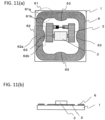
- FIGS. 11(a) and 11(b) are a top view and a cross-sectional view of the substrate 1 of the semiconductor light-emitting device according to Embodiment 2.
- the semiconductor light-emitting device according to Embodiment 2 has the same configuration as the device of Embodiment 1, but is different from Embodiment 1 in that convex portions 63 that project to the semiconductor light-emitting element 3 side are provided in the edges 62b on the inner peripheral sides of the straight-line portions 62 of the bonding pattern 6 on the substrate 1.
- the shape of the edge of the convex portions 63 is a substantially arc shape in the present embodiment.
- the positions where the convex portions 63 are provided are intermediate points between the corner portions 61.
- the convex portions 63 are provided at four positions.
- the tips of the convex portions 63 of the bonding pattern 6 preferably project to the semiconductor light-emitting element 3 side from an inner peripheral edge 42 of the annular base portion 4c of the dome-shaped transparent body 4.
- the shape of the bonding pattern 5 of the dome-shaped transparent body 4 is the same as in Embodiment 1 (see FIG. 5 ). That is, the bonding pattern 5 on the dome-shaped transparent body 4 side does not have a convex portion shape corresponding to the convex portions 63 of the bonding pattern 5 on the substrate 1 side.
- the bonding pattern 6 made of metal includes the wide convex portions 63, when the substrate 1 is heated in the manufacturing process of bonding the dome-shaped transparent body 4, the temperature of the convex portions 63 is higher than that of the surroundings. Also, parts of the bonding patterns 5 and 6 of the straight-line portions 62 that are adjacent to the convex portions 63 overlap with the base portion 4c of the dome-shaped transparent body 4 and thus are pressed by the base portion 4c at the time of bonding, so that the solder 7 is first melted.
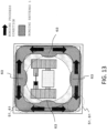
- melting start positions are fixed to the bonding patterns 5 and 6 of the straight-line portions 62 adjacent to the convex portions 63, and thus the flow of the melted solder directed from the straight-line portions 62 to the corner portions 61 as illustrated in FIG. 13 can be generated more clearly than in Embodiment 1, so that a settled bonding layer can be formed.
- flows of melted solder collide with each other at fewer locations, and the generation of voids can be suppressed. Accordingly, the generation of voids that connect the space 8 inside the dome-shaped transparent body 4 to an outside space can be suppressed.
- the semiconductor light-emitting device according to Embodiment 2 can suppress the generation of solder balls more than the semiconductor light-emitting device according to Embodiment 1.
- solder 7 it is required to sufficiently supply the solder 7 to form the bonding layer 7a, but when the amount of the solder 7 is too much, the excess solder 7 protrudes from the bonding patterns 5 and 6 as illustrated in FIG. 7 but does not wet the front surface of the substrate 1, so that a solder ball 71 that hardens into a ball shape is likely formed.
- the solder ball 71 may protrude into the space 8 and become visible to cause a poor appearance and may reach the electrode 2 on the substrate 1 to cause a decrease in reliability, such as a non-lighting of the light-emitting element.
- the protrusion of the solder ball 71 into the space 8 is more likely to occur on the cross section taken along line C-C' as illustrated in FIG. 7(a) than on the cross section taken along line D-D' .
- the solder wets and spreads to the convex portions 63 and thus can be maintained by surface tension, so that it is possible to suppress protrusion of the solder 7 from the bonding pattern 6 to form solder balls. That is, it is possible to increase the degree of freedom in designing the solder 7 to form the bonding layer 7a with high reliability.
- Embodiment 2 Other configurations, functions and effects of the device of Embodiment 2 are the same as those of Embodiment 1, so description thereof is omitted.
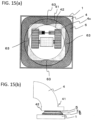
- FIGS. 15 (a) and 15 (b) illustrate a top view and a cross-sectional view of the semiconductor light-emitting device according to Modification 1 of Embodiment 2.
- the tips of the convex portions 63 project to the semiconductor light-emitting element 3 side from the edge 42 on the inner side of the base portion 4c of the dome-shaped transparent body 4.
- the tips of the convex portions 63 may be positioned on the outer side of the edge 42 on the inner side of the base portion 4c.
- FIGS. 16(a) and 16(b) A top view and a cross-sectional view of the semiconductor light-emitting device according to Modification 2 of Embodiment 2 are illustrated in FIGS. 16(a) and 16(b) .
- the convex portions 63 are provided in the bonding pattern 6 on the substrate 1 side, but a convex portion is not provided in the bonding pattern 5 of the dome-shaped transparent body 4.
- convex portions 64 may also be provided in the bonding pattern 5 of the dome-shaped transparent body 4.
- the convex portions 64 are provided at positions facing the convex portions 63.
- the shape of the convex lid portion 4a of the dome-shaped transparent body 4 may be a shape in which the inside space 8 is convex with respect to the substrate 1. Therefore, in the convex lid portion 4a, the space 8 may have a hemispherical shape and may have a semi-ellipsoidal shape.
- an outer shape of the convex lid portion 4a is not limited to a hemispherical shape or a semi-ellipsoidal shape, and may be any shape.
- the outer shape of the convex lid portion 4a may be a rectangular parallelepiped shape.
- the base portion 4c of the convex lid portion 4a is not limited to a circular shape and may have an oval shape.
- Embodiment 3 a water disinfection device using the semiconductor light-emitting devices according to Embodiments 1 and 2 and Modifications 1 and 2 is described.
- a semiconductor light-emitting device and a drive circuit thereof are disposed in a supply channel for supplying water.
- the semiconductor light-emitting device irradiates water flowing through the supply channel with deep ultraviolet light for disinfection.
- the semiconductor light-emitting devices of Embodiments 1 and 2 and Modifications 1 and 2 can be used as an LED package that seals a deep-ultraviolet LED as the semiconductor light-emitting element 3.
- the semiconductor light-emitting devices can be used as a laser package that seals a surface emitting laser as the semiconductor light-emitting element.
Landscapes
- Physics & Mathematics (AREA)
- Condensed Matter Physics & Semiconductors (AREA)
- General Physics & Mathematics (AREA)
- Electromagnetism (AREA)
- Optics & Photonics (AREA)
- Health & Medical Sciences (AREA)
- Life Sciences & Earth Sciences (AREA)
- Environmental & Geological Engineering (AREA)
- Chemical & Material Sciences (AREA)
- Organic Chemistry (AREA)
- Water Supply & Treatment (AREA)
- Engineering & Computer Science (AREA)
- Toxicology (AREA)
- Hydrology & Water Resources (AREA)
- Veterinary Medicine (AREA)
- Epidemiology (AREA)
- Public Health (AREA)
- Animal Behavior & Ethology (AREA)
- General Health & Medical Sciences (AREA)
- Led Device Packages (AREA)
- Semiconductor Lasers (AREA)
Abstract
Description
- The present invention relates to a semiconductor light-emitting device in which a space around a semiconductor light-emitting element is sealed airtightly.
- In the related art, for example, an airtight package in a semiconductor light-emitting device that requires airtightness uses a structure in which a flat plate-shaped translucent optical element is bonded to a cavity-type substrate as disclosed in
PTL 1, or a structure in which a cavity-type translucent optical element is bonded to a flat plate-shaped substrate as disclosed inPTL 2. For example, an optical element such as glass and a heat dissipation substrate such as a ceramic substrate are bonded to each other and sealed by solder such as AuSn or a brazing material. - In addition, in an airtight package as described above, when a translucent optical element is bonded to a substrate by using solder, there is a problem that the solder protrudes outside a bonding pattern.
PTL 3 suggests a structure of suppressing protrusion of solder from a bonding pattern by forming a film such as an oxide film that has poor solder wettability in an inner peripheral portion and an outer peripheral portion of a bonding area. In addition,PTL 4 suggests a structure in which a recessed structure is formed on a substrate and protruding solder is accommodated in a recessed portion to suppress wetting and spreading of the solder outside of the recessed portion. -
- PTL 1:
JP2015-18873A - PTL 2:
JP5838357B - PTL 3:
JP2015-073027A - PTL 4:
JP2007-103909A - In an airtight package, a configuration of suppressing a problem that solder melted when an optical element and a heat dissipation substrate are bonded to each other protrudes from a bonding pattern by forming an oxide film or a groove in advance on a substrate as disclosed in
PTLS - An object of the invention is to newly provide a semiconductor light-emitting device having high airtight reliability by increasing bonding reliability between a substrate and a lid.
- In order to achieve the object, a semiconductor light-emitting device according to the invention includes a substrate; a semiconductor light-emitting element that is mounted on the substrate; and a dome-shaped transparent body that is mounted on the substrate. The dome-shaped transparent body includes a convex lid portion that covers a space around the semiconductor light-emitting element and includes an annular base portion and a flange portion that projects to an outer side of an outer peripheral edge of the annular base portion. A first bonding pattern made of metal that surrounds the semiconductor light-emitting element is formed on the substrate. A second bonding pattern having a shape corresponding to the first bonding pattern is provided in the base portion and the flange portion of the dome-shaped transparent body. The first bonding pattern and the second bonding pattern are bonded to each other via solder, to seal the space in the convex lid portion. The first bonding pattern and the second bonding pattern have rectangular ring shapes that surround the semiconductor light-emitting element when viewed from above, at least edges on inner peripheral sides of corner portions thereof are positioned on outer sides of outer peripheral edges of the annular base portion of the convex lid portion, and at least edges on inner peripheral sides of straight-line portions sandwiched between the corner portions are positioned closer to the semiconductor light-emitting element than the outer peripheral edge of the annular base portion of the convex lid portion.
- According to the invention, a bonding pattern between a substrate and a dome-shaped transparent body has a rectangular ring shape when viewed from above, corner portions thereof are positioned on outer sides of an annular base portion of a convex lid portion to which a load is applied when a dome-shaped transparent body is pressed at the time of bonding, and thus it is possible to provide a semiconductor light-emitting device in which generation of voids in a bonding portion is suppressed, bonding reliability is high, and airtight reliability is high.
-
- [
FIG. 1] FIG. 1(a) is a top view of a semiconductor light-emitting device according toEmbodiment 1 andFIG. 1(b) is a cross-sectional view thereof taken along the line A-A'. - [
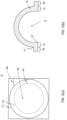
FIG. 2] FIG. 2(a) is a top view of a dome-shapedtransparent body 4 of the semiconductor light-emitting device according toEmbodiment 1 andFIG. 2(b) is a cross-sectional view thereof. - [
FIG. 3] FIG. 3 is a cross-sectional view of the semiconductor light-emitting device according toEmbodiment 1 taken along the line B-B'. - [
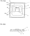
FIG. 4] FIG. 4(a) is a top view of asubstrate 1 of the semiconductor light-emitting device according toEmbodiment 1, andFIG. 4(b) is a cross-sectional view thereof. - [
FIG. 5] FIG. 5(a) is a top view of a state in which abonding pattern 5 of the dome-shapedtransparent body 4 of the semiconductor light-emitting device according toEmbodiment 1 is provided, andFIG. 5(b) is a cross-sectional view thereof. - [
FIG. 6] FIG. 6(a) is an explanatory view illustrating a flow of meltedsolder 7 in a bonding process when the semiconductor light-emitting device according toEmbodiment 1 is manufactured, andFIG. 6(b) is an explanatory view illustrating a flow of the meltedsolder 7 in a bonding process when a semiconductor light-emitting device according to a comparative example is manufactured. - [
FIG. 7] FIG. 7(a) is a cross-sectional view of a state in which thesolder 7 wets and spreads to the bonding pattern in the bonding process of the semiconductor light-emitting device according toEmbodiment 1, taken along the line C-C', andFIG. 7(b) is a cross-sectional view thereof taken along the line D-D'. - [
FIG. 8] FIG. 8 is a cross-sectional view illustrating an example of layer structures ofbonding patterns Embodiment 1. - [
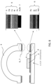
FIG. 9] FIGS. 9(a) and 9(b) are bottom views illustrating states in which the solder 7 (before melting) is mounted on thebonding pattern 5 on a dome-shapedtransparent body 4 side in a manufacturing process of the semiconductor light-emitting device according to Embodiment 1. - [
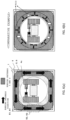
FIG. 10] FIG. 10(a) is a top view of a semiconductor light-emitting device according toEmbodiment 2, andFIG. 10(b) is a cross-sectional view thereof taken along the line E-E' . - [
FIG. 11] FIG. 11(a) is a top view of thesubstrate 1 of the semiconductor light-emitting device according toEmbodiment 2, andFIG. 11(b) is a cross-sectional view thereof. - [
FIG. 12 ] FIG. 12(a) is a top view of the semiconductor light-emitting device according toEmbodiment 2, and FIG. 12(b) is a cross-sectional view thereof taken along the line F-F'. - [
FIG. 13] FIG. 13 is an explanatory view illustrating a flow of the meltedsolder 7 in a bonding process when the semiconductor light-emitting device according to Embodiment 2 is manufactured. - [
FIG. 14] FIG. 14 is a cross-sectional view of a state in which thesolder 7 wets and spreads to a bonding pattern in the semiconductor light-emitting device according toEmbodiment 2. - [
FIG. 15] FIG. 15(a) is a top view of a semiconductor light-emitting device according toModification 1 ofEmbodiment 2, andFIG. 15(b) is a cross-sectional view thereof. - [
FIG. 16] FIG. 16(a) is a top view of a semiconductor light-emitting device according toModification 2 ofEmbodiment 2, andFIG. 16(b) is a cross-sectional view thereof. - Hereinafter, a semiconductor light-emitting device according to an embodiment of the invention is described.
- A configuration of a semiconductor light-emitting device according to
Embodiment 1 is described with reference toFIG. 1 to FIG. 7 . - A top view and a cross-sectional view of the semiconductor light-emitting device according to
Embodiment 1 are illustrated inFIGS. 1(a) and 1(b) . - The semiconductor light-emitting device according to
Embodiment 1 includes asubstrate 1, a semiconductor light-emittingelement 3 mounted on anelectrode 2 on thesubstrate 1, and a dome-shapedtransparent body 4 mounted on thesubstrate 1. - As illustrated in a top view and a cross-sectional view of
FIGS. 2(a) and 2(b) , the dome-shapedtransparent body 4 covers a space around the semiconductor light-emittingelement 3 and includes aconvex lid portion 4a including anannular base portion 4c and aflange portion 4b projecting to an outer side of an outer peripheral edge of theannular base portion 4c. According to the present embodiment, thebase portion 4c has an annular shape with a predetermined width. As illustrated inFIGS. 2(a) and 2(b) , thebase portion 4c is a root portion of theconvex lid portion 4a that configures a bottom surface with a thickness of theconvex lid portion 4a, in the dome-shapedtransparent body 4. - According to the present embodiment, both the
substrate 1 and theflange portion 4b have rectangular shapes when viewed from above, and the dome-shapedtransparent body 4 is mounted on thesubstrate 1 so that directions of corner portions are the same. The size of theflange portion 4b is slightly smaller than that of thesubstrate 1 in the present embodiment. - As illustrated in an enlarged cross-sectional view of
FIG. 3 , theannular base portion 4c and theflange portion 4b of the dome-shapedtransparent body 4, and thesubstrate 1 in contact with theannular base portion 4c and theflange portion 4b are respectively provided with thebonding patterns bonding patterns flange portion 4b and thesubstrate 1. - A top view and a cross-sectional view of the
substrate 1 in which thebonding pattern 6 is provided are illustrated inFIGS. 4(a) and 4(b) . In addition, a top view and a cross-sectional view of the dome-shapedtransparent body 4 in which thebonding pattern 5 is provided are illustrated inFIGS. 5(a) and 5(b) . As seen fromFIG. 4(a) ,FIG. 5(a) , andFIGS. 1(a) and 1(b) , when viewed from above, thebonding patterns element 3, and have rectangular ring shapes. - The
bonding pattern 5 provided in the dome-shapedtransparent body 4 includes four straight-line portions 52 formed along the sides that configure the outer shape of the dome-shapedtransparent body 4 andcorner portions 51 that connect between the adjacent straight-line portions 52. - The
bonding pattern 6 provided on thesubstrate 1 includes four straight-line portions 62 formed along the sides that configure the outer shape of thesubstrate 1 andcorner portions 61 that connect the adjacent straight-line portions 62. - The
bonding patterns solder 7, to form abonding layer 7a (seeFIG. 3 ). Accordingly, aspace 8 in theconvex lid portion 4 is sealed. Thebonding layer 7a wets and spreads along the bonding pattern and has a fillet shape as a whole end portion. In addition, the terminal end portion may have a slightly raised shape due to the action of surface tension. In addition, thesolder 7 may be in contact with the side surface of thebonding pattern 5. - The width of the
bonding pattern 5 on atransparent body 4 side is preferably narrower than the width of thebonding pattern 6 on asubstrate 1 side. - Here, the
corner portions bonding patterns peripheral edge 41 of theannular base portion 4c of theconvex lid portion 4a (seeFIG. 1(a) ). In addition, edges 51b and 61b on an inner peripheral side of thecorner portions bonding patterns peripheral edge 41 of theannular base portion 4c of theconvex lid portion 4a. - Accordingly, the
bonding pattern 5 provided in the dome-shapedtransparent body 4 is provided so that the straight-line portion 52 partially overlaps with thebase portion 4c, and at least a part of thecorner portion 51 is provided to be positioned on an outer side of thebase portion 4c. That is, an area that does not overlap with thebase portion 4c is provided in thecorner portion 51. - Meanwhile, the straight-
line portions bonding patterns element 3 side of the outerperipheral edge 41 of theannular base portion 4c of theconvex lid portion 4a (seeFIG. 1(a) ). In addition, edges 52a and 62a on the outer peripheral side of the straight-line portions bonding patterns peripheral edge 41 of thebase portion 4c. - Accordingly, the
bonding pattern 6 provided on thesubstrate 1 is provided so that the straight-line portion 62 partially overlaps with thebase portion 4c, and at least a part of thecorner portion 61 is provided to be positioned on the outer side of thebase portion 4c. That is, an area that does not overlap with thebase portion 4c is provided in thecorner portion 61. - In this manner, the semiconductor light-emitting device according to the present embodiment uses the
bonding patterns corner portions peripheral edge 41 of theannular base portion 4c to which a load is most applied, the load being applied to theconvex lid portion 4a when the dome-shapedtransparent body 4 is bonded. Meanwhile, the straight-line portions bonding patterns base portion 4c to which a load is most applied. Accordingly, in the bonding process, the loads applied to thecorner portions bonding patterns line portions - Accordingly, in a manufacturing process, when the
substrate 1 is heated while a load is applied in a direction of pressing the dome-shapedtransparent body 4 to thesubstrate 1, thesolder 7 disposed between thebonding patterns line portions base portion 4c overlaps in a thickness direction). At the time of the melting start, thesolder 7 in an area sandwiched between thecorner portions 51 and 61 (an area where thebase portion 4c does not overlap in the thickness direction) is not melted but is melted thereafter. Accordingly, as illustrated inFIG. 6(a) , the melting direction of thesolder 7 can be directed from a center of the straight-line portions corner portions line portions corner portions - In the semiconductor light-emitting device according to the present embodiment, the bonding progresses together with the melting of the
solder 7 from the straight-line portions bonding patterns corner portions corner portions - In this manner, in the device according to the present embodiment, the
bonding layer 7a settled by thesolder 7 can be formed, and also generation of voids that connect thespace 8 inside the dome-shapedtransparent body 4 to an outside space can be suppressed. Accordingly, it is possible to provide the semiconductor light-emitting device having high airtightness. - In addition, the
bonding patterns - As the
solder 7, for example, AuSn solder can be used. The form of the solder at the time of supplying the solder in the manufacturing process may be a sheet shape or may be a dot shape. - As the semiconductor light-emitting
element 3, a light emitting diode (LED) and a laser light emitting diode (including a surface emitting laser) can be used. As the semiconductor light-emittingelement 3, a semiconductor light-emitting element having an appropriate light emission wavelength according to the use of the semiconductor light-emitting device and emitting ultraviolet light, visible light, or infrared light can be selected. The dome-shapedtransparent body 4 is configured with a material that transmits light emitted from the semiconductor light-emittingelement 3. - For example, as the semiconductor light-emitting
element 3, an element that emits ultraviolet light having a wavelength band of 210 nm or more and 310 nm or less can be used. - In this case, for the dome-shaped
transparent body 4, one in which at least theconvex lid portion 4a is configured with a material (for example, quartz, borosilicate glass, and sapphire glass) that transmits deep ultraviolet rays can be used. - The semiconductor light-emitting
element 3 is configured with a compound semiconductor and at least includes a p-type semiconductor layer, a light-emitting layer, and an n-type semiconductor layer. In addition, as a light emitting diode that emits ultraviolet light having a wavelength of 200 nm to 405 nm, an aluminum nitride-based, gallium nitride-based, or aluminum gallium nitride-based semiconductor light-emitting element can be used. - The semiconductor light-emitting
element 3 is mounted on theelectrode 2 formed on thesubstrate 1, with an appropriate bonding material. According to the present embodiment, the semiconductor light-emittingelement 3 is mounted with an AuSn bonding material. - The semiconductor light-emitting
element 3 can be mounted on theelectrode 2 via a submount substrate (not illustrated). In addition, the number of elements mounted on one substrate may not be one. Thesubstrate 1 is not limited to a flat plate shape as in the present embodiment and can be a shape including a recessed portion at a position where the semiconductor light-emittingelement 3 is mounted. - Aluminum nitride (AlN) which is a base material that can maintain airtightness can be used as the
substrate 1. As the base material, ceramics made of nitrides, carbides, or oxides such as silicon nitride (Si3N4), silicon carbide (SiC), and aluminum oxide (Al2O3) can be used in addition to aluminum nitride (AlN). Thesubstrate 1 may be a hightemperature fired ceramic substrate or a low-temperature fired ceramic substrate. By using thesubstrate 1 of a ceramic base material, since heat generated by the semiconductor light-emittingelement 3 can be effectively dissipated, and also the semiconductor light-emittingelement 3 has ultraviolet resistance, even when the semiconductor light-emittingelement 3 emits ultraviolet light, light output can be maintained for a long period of time. - The semiconductor light-emitting
element 3 is mounted on theelectrode 2 formed on thesubstrate 1. Theelectrode 2 is formed in connection with a back surface electrode (not illustrated) that is electrically connected to the semiconductor light-emitting element and formed on the back surface of thesubstrate 1 and a through electrode that is formed to penetrate thesubstrate 1, for electric supply from the outside to the semiconductor light-emittingelement 3. In addition to the semiconductor light-emittingelement 3, other electronic components such as Zener diodes and photodiodes can be mounted on theelectrode 2 depending on the application. - A material that reduces a refractive index difference between the semiconductor light-emitting
element 3 and the dome-shapedtransparent body 4 may be disposed in ahollow portion 8. - On the front surface of the bottom surface (the surfaces of the
flange portion 4b and thebase portion 4c on thesubstrate 1 side) of the dome-shapedtransparent body 4, fine irregularities, that is, coarseness, can be formed. Due to the coarseness of the bottom surface of thetransparent body 4, the outer side of a lens is slightly curved, and thus at the time of bonding, the bonding can progress in a direction from the inner side to the outer side, and thus it is possible to provide the semiconductor light-emitting device with higher bonding stability. In order to avoid defective bonding caused by an excessively large warpage amount, it is preferable to set the coarseness amount so that the warpage amount (height difference between the inner side and the outer side of the bottom surface of the dome-shaped transparent body 4) is smaller than the thickness of thebonding pattern 6 on the substrate side. - An example of a method of manufacturing the semiconductor light-emitting device according to the present embodiment is described.
- For example, the
substrate 1 made of AlN is prepared, and thebonding pattern 6 having the rectangular ring shape and theelectrode 2 as described above are formed. For example, as illustrated inFIG. 8 , the layer structure of thebonding pattern 6 is a structure obtained by sequentially stacking a NiCr layer, an Au layer, a Ni layer, and an Au layer in order from thesubstrate 1 side. The uppermost layer of thebonding pattern 6 is preferably made of a material that is melted at the time of bonding and mixed with the meltedsolder 7 to change the composition of thesolder 7, so that a eutectic bonding layer with a melting point higher than thesolder 7 can be formed. For example, when AuSn of thesolder 7 is used, the uppermost layer of thebonding pattern 6 is preferably an Au layer. - Meanwhile, the dome-shaped
transparent body 4 made of quartz glass is prepared, and thebonding pattern 5 having the rectangular ring shape as described above is formed on thebase portion 4c and theflange portion 4b. For example, as illustrated inFIG. 8 , the layer structure of thebonding pattern 5 is a structure obtained by stacking a Ti layer, a Pd layer, a Cu layer, a Ni layer, and an Au layer in order from a dome-shapedtransparent body 4 side. The uppermost layer of thebonding pattern 5 is preferably made of a material that is melted at the time of bonding and mixed with the meltedsolder 7 to change the composition of thesolder 7, so that a eutectic bonding layer with a melting point higher than thesolder 7 can be formed. For example, when AuSn of thesolder 7 is used, the uppermost layer of thebonding pattern 5 is preferably an Au layer. - The
solder 7 used for bonding adheres to the front surface of thebonding pattern 5 of the dome-shapedtransparent body 4. Thesolder 7 for bonding is, for example, made of AuSn. The shape thereof may be the same as the shape of thebonding pattern 5 having the rectangular ring shape as illustrated inFIG. 9(a) and have a sheet shape in which the width is narrower than thebonding pattern 5 or may be dot-shaped solder as illustrated inFIG. 9(b) . - The
solder 7 having a sheet shape temporarily adheres to thebonding pattern 5 by partial laser welding. The meltedsolder 7 is scattered in a dot shape, and the dot-shapedsolder 7 is welded to thebonding pattern 5. The diameter of the dot-shapedsolder 7 is smaller than the width of thebonding pattern 5. The number of items of the dot-shapedsolder 7 welded onto thebonding pattern 5 is preferably 20 to 36 and more preferably 28. - In both cases of the sheet shape and the dot shape, with respect to the composition ratio of Au and Sn of the
AuSn solder 7, the Au concentration is preferably 73 wt% to 83 wt%, and the Au concentration is more preferably 78 wt%. - Then, the semiconductor light-emitting
element 3 made of an AlGaN-based material, which emits ultraviolet light having a wavelength of 210 nm or more and 310 nm or less, is mounted to theelectrode 2 of thesubstrate 1. - Then, the dome-shaped
transparent body 4 is mounted on thesubstrate 1 so that the semiconductor light-emittingelement 3 of thesubstrate 1 is covered, and is aligned so that thebonding pattern 5 and thebonding pattern 6 overlap with each other. - Then, a load is applied to the vertex of the dome-shaped
transparent body 4, and thesolder 7 is heated and melted while the dome-shapedtransparent body 4 is pressed to thesubstrate 1. - Specifically, first, the
substrate 1 on which the semiconductor light-emitting element is mounted and the dome-shapedtransparent body 4 are set into a bonding device that can adjust filled gas. The dome-shapedtransparent body 4 is set so that the opening faces upward, and the substrate is set above the dome-shapedtransparent body 4 so that the side on which the semiconductor light-emitting element is mounted faces downward. Next, moisture is removed by heating thesubstrate 1 to the temperature that is slightly lower than the temperature at which thesolder 7 is melted and causing the bonding device to be in a vacuum state. Thereafter, while the inside of the bonding device is replaced with nitrogen gas at atmospheric pressure, the top of the dome-shapedtransparent body 4 is pushed up by a movable portion of the bonding device, and the dome-shapedtransparent body 4 is pressed against thesubstrate 1 from below to seal thespace 8. Next, thesubstrate 1 is heated to the melting temperature of thesolder 7 and is cooled down after being maintained for a predetermined period of time, to form a bonding portion and airtightly seal thespace 8. - Accordingly, as illustrated in
FIG. 6(a) , first, thesolder 7 of the straight-line portions bonding pattern 5 is melted and flows to thecorner portions solder 7 of thecorner portions bonding patterns solder 7. - The
solder 7 is melted, to form the bonding layer. - With the above, the semiconductor light-emitting device that emits ultraviolet light can be manufactured.
- Since the corner portions of the
bonding pattern 5 are disposed on the outer side of thebase portion 4c to which a load is applied, the manufactured semiconductor light-emitting device can suppress the protrusion of thesolder 7 into thespace 8. In addition, the generation of the void can be prevented. - In addition, since an airtight space is formed by covering the semiconductor light-emitting
element 3 with the dome-shaped transparent body 4 (quartz glass) having a curved surface on the front surface, total reflection is less likely to occur, and the light extraction efficiency increases. - As Comparative Example 1,
FIG. 6(b) illustrates a method of progressing the melting of thesolder 7 when thebonding patterns base portion 4c andflange portion 4b. - With respect to the
bonding patterns edges edges Embodiment 1, with respect to thebonding patterns edges peripheral edge 41 of theannular base portion 4c of theconvex lid portion 4a. However, differently fromEmbodiment 1, with respect to thebonding patterns edges peripheral edge 41 of theannular base portion 4c of theconvex lid portion 4a over the entire circumference. - In this configuration of Comparative Example 1, as a result of X-ray transmission observation, bubbles are generated in the
bonding layer 7a on thebonding patterns Embodiment 1. In the X-ray transmission observation on a sample of the semiconductor light-emitting device according toEmbodiment 1, the obvious generation of bubbles in thebonding layer 7a is not recognized. It is considered that this is because, in the semiconductor light-emitting device according to Comparative Example 1, melting starts from a plurality of positions of thebase portion 4c to which loads are applied, bonding portions resultantly formed by progress of the bonding from many directions collide with each other, and the colliding position is the cause of the generation of the void. In addition, positions where the voids are generated are random. Therefore, it is concerned that voids that connect thespace 8 inside the dome-shapedtransparent body 4 to an outside space are generated. - A semiconductor light-emitting device according to
Embodiment 2 is described with reference toFIG. 10 to FIG. 14 .FIGS. 10(a) and 10(b) are a top view and a cross-sectional view of a semiconductor light-emitting device according toEmbodiment 2.FIGS. 11(a) and 11(b) are a top view and a cross-sectional view of thesubstrate 1 of the semiconductor light-emitting device according toEmbodiment 2. - As illustrated in
FIG. 10 ,FIG. 11 , andFIG. 12 , the semiconductor light-emitting device according toEmbodiment 2 has the same configuration as the device ofEmbodiment 1, but is different fromEmbodiment 1 in thatconvex portions 63 that project to the semiconductor light-emittingelement 3 side are provided in theedges 62b on the inner peripheral sides of the straight-line portions 62 of thebonding pattern 6 on thesubstrate 1. The shape of the edge of theconvex portions 63 is a substantially arc shape in the present embodiment. The positions where theconvex portions 63 are provided are intermediate points between thecorner portions 61. Theconvex portions 63 are provided at four positions. - As illustrated in
FIGS. 10(a) and 10(b) , andFIG. 12 , the tips of theconvex portions 63 of thebonding pattern 6 preferably project to the semiconductor light-emittingelement 3 side from an innerperipheral edge 42 of theannular base portion 4c of the dome-shapedtransparent body 4. - The shape of the
bonding pattern 5 of the dome-shapedtransparent body 4 is the same as in Embodiment 1 (seeFIG. 5 ). That is, thebonding pattern 5 on the dome-shapedtransparent body 4 side does not have a convex portion shape corresponding to theconvex portions 63 of thebonding pattern 5 on thesubstrate 1 side. - Since the
bonding pattern 6 made of metal includes the wideconvex portions 63, when thesubstrate 1 is heated in the manufacturing process of bonding the dome-shapedtransparent body 4, the temperature of theconvex portions 63 is higher than that of the surroundings. Also, parts of thebonding patterns line portions 62 that are adjacent to theconvex portions 63 overlap with thebase portion 4c of the dome-shapedtransparent body 4 and thus are pressed by thebase portion 4c at the time of bonding, so that thesolder 7 is first melted. Therefore, melting start positions are fixed to thebonding patterns line portions 62 adjacent to theconvex portions 63, and thus the flow of the melted solder directed from the straight-line portions 62 to thecorner portions 61 as illustrated inFIG. 13 can be generated more clearly than inEmbodiment 1, so that a settled bonding layer can be formed. In addition, flows of melted solder collide with each other at fewer locations, and the generation of voids can be suppressed. Accordingly, the generation of voids that connect thespace 8 inside the dome-shapedtransparent body 4 to an outside space can be suppressed. - In addition, the semiconductor light-emitting device according to
Embodiment 2 can suppress the generation of solder balls more than the semiconductor light-emitting device according toEmbodiment 1. - Here, in the semiconductor light-emitting device according to
Embodiment 1, it is required to sufficiently supply thesolder 7 to form thebonding layer 7a, but when the amount of thesolder 7 is too much, theexcess solder 7 protrudes from thebonding patterns FIG. 7 but does not wet the front surface of thesubstrate 1, so that asolder ball 71 that hardens into a ball shape is likely formed. Thesolder ball 71 may protrude into thespace 8 and become visible to cause a poor appearance and may reach theelectrode 2 on thesubstrate 1 to cause a decrease in reliability, such as a non-lighting of the light-emitting element. Particularly, the protrusion of thesolder ball 71 into thespace 8 is more likely to occur on the cross section taken along line C-C' as illustrated inFIG. 7(a) than on the cross section taken along line D-D' . - In contrast, in the semiconductor light-emitting device according to
Embodiment 2, even when the amount ofsolder 7 is large, as illustrated inFIG. 14 , the solder wets and spreads to theconvex portions 63 and thus can be maintained by surface tension, so that it is possible to suppress protrusion of thesolder 7 from thebonding pattern 6 to form solder balls. That is, it is possible to increase the degree of freedom in designing thesolder 7 to form thebonding layer 7a with high reliability. - Accordingly, it is possible to prevent a solder ball from being in contact with the
electrode 2 to cause a short circuit, and thus the occurrence of defects can be suppressed. - Other configurations, functions and effects of the device of
Embodiment 2 are the same as those ofEmbodiment 1, so description thereof is omitted. -
FIGS. 15 (a) and 15 (b) illustrate a top view and a cross-sectional view of the semiconductor light-emitting device according toModification 1 ofEmbodiment 2. In the configuration ofEmbodiment 2 illustrated inFIGS. 10(a) and 10(b) , the tips of theconvex portions 63 project to the semiconductor light-emittingelement 3 side from theedge 42 on the inner side of thebase portion 4c of the dome-shapedtransparent body 4. However, as in the device ofModification 1 illustrated inFIGS. 15(a) and 15(b) , the tips of theconvex portions 63 may be positioned on the outer side of theedge 42 on the inner side of thebase portion 4c. - A top view and a cross-sectional view of the semiconductor light-emitting device according to
Modification 2 ofEmbodiment 2 are illustrated inFIGS. 16(a) and 16(b) . In the configuration ofEmbodiment 2 illustrated inFIGS. 10(a) and 10(b) , theconvex portions 63 are provided in thebonding pattern 6 on thesubstrate 1 side, but a convex portion is not provided in thebonding pattern 5 of the dome-shapedtransparent body 4. As inModification 2 illustrated inFIGS. 16(a) and 16(b) ,convex portions 64 may also be provided in thebonding pattern 5 of the dome-shapedtransparent body 4. Theconvex portions 64 are provided at positions facing theconvex portions 63. - In addition, in
Embodiments Modifications convex lid portion 4a of the dome-shapedtransparent body 4 may be a shape in which theinside space 8 is convex with respect to thesubstrate 1. Therefore, in theconvex lid portion 4a, thespace 8 may have a hemispherical shape and may have a semi-ellipsoidal shape. - In addition, an outer shape of the
convex lid portion 4a is not limited to a hemispherical shape or a semi-ellipsoidal shape, and may be any shape. For example, the outer shape of theconvex lid portion 4a may be a rectangular parallelepiped shape. - Further, the
base portion 4c of theconvex lid portion 4a is not limited to a circular shape and may have an oval shape. - As
Embodiment 3, a water disinfection device using the semiconductor light-emitting devices according toEmbodiments Modifications - In the water disinfection device, a semiconductor light-emitting device and a drive circuit thereof are disposed in a supply channel for supplying water. The semiconductor light-emitting device irradiates water flowing through the supply channel with deep ultraviolet light for disinfection.
- In addition, the semiconductor light-emitting devices of
Embodiments Modifications element 3. In addition, the semiconductor light-emitting devices can be used as a laser package that seals a surface emitting laser as the semiconductor light-emitting element. -
- 1:
- substrate
- 2:
- electrode
- 3:
- semiconductor light-emitting element
- 4:
- dome-shaped transparent body
- 4a:
- convex lid portion
- 4b:
- flange portion
- 4c:
- base portion
- 5, 6:
- bonding pattern
- 7:
- solder
- 8:
- space
- 41:
- outer peripheral edge of base portion
- 42:
- inner peripheral edge of base portion
- 51, 61:
- corner portion of bonding pattern
- 52, 62:
- straight-line portion of bonding pattern
- 63, 64:
- convex portion
Claims (13)
- A semiconductor light-emitting device comprising:a substrate;a semiconductor light-emitting element that is mounted on the substrate; anda dome-shaped transparent body that is mounted on the substrate,wherein the dome-shaped transparent body includes a convex lid portion that covers a space around the semiconductor light-emitting element and includes an annular base portion and a flange portion that projects to an outer side of an outer peripheral edge of the annular base portion,a first bonding pattern made of metal that surrounds the semiconductor light-emitting element is formed on the substrate,a second bonding pattern having a shape corresponding to the first bonding pattern is provided in the base portion and the flange portion of the dome-shaped transparent body, and the first bonding pattern and the second bonding pattern are bonded to each other via solder, to seal the space in the convex lid portion, andthe first bonding pattern and the second bonding pattern have rectangular ring shapes that surround the semiconductor light-emitting element when viewed from above, at least edges on inner peripheral sides of corner portions thereof are positioned on outer sides of outer peripheral edges of the annular base portion of the convex lid portion, and at least edges on inner peripheral sides of straight-line portions sandwiched between the corner portions are positioned closer to the semiconductor light-emitting element than the outer peripheral edge of the annular base portion of the convex lid portion.
- The semiconductor light-emitting device according to claim 1, wherein
the base portion has an annular shape. - The semiconductor light-emitting device according to claim 1 or 2, wherein
a width of the second bonding pattern is narrower than a width of the first bonding pattern. - The semiconductor light-emitting device according to any one of claims 1 to 3, wherein
a convex portion that projects to the semiconductor light-emitting element side is provided at an edge on the inner peripheral side at an intermediate point between corner portions of the straight-line portion of the first bonding pattern. - The semiconductor light-emitting device according to claim 4, wherein
a tip of the convex portion of the first bonding pattern projects to the semiconductor light-emitting element side from an inner peripheral edge of the annular base portion of the convex lid portion. - The semiconductor light-emitting device according to claim 4, wherein
the second bonding pattern does not include a convex portion corresponding to the convex portion of the first bonding pattern. - The semiconductor light-emitting device according to any one of claims 1 to 6, whereinan outer shape of the flange portion of the dome-shaped transparent body is a rectangular shape, andthe first bonding pattern and the second bonding pattern are provided along the outer shape of the flange portion.
- The semiconductor light-emitting device according to any one of claims 1 to 7, wherein
the first bonding pattern is formed with any metal among Ni, Cr, Au, Cu, Pt, Ti, Pd, and W, or a stacked body of layers made of two or more kinds of metal among the metal. - The semiconductor light-emitting device according to claim 1, wherein
the solder is an AuSn solder. - The semiconductor light-emitting device according to any one of claims 1 to 9, wherein
a convex lid portion of the dome-shaped transparent body is configured with a material that transmits deep ultraviolet rays. - The semiconductor light-emitting device according to any one of claims 1 to 10, wherein
the semiconductor light-emitting element emits ultraviolet light having a wavelength band of 210 nm or more and 310 nm or less. - The semiconductor light-emitting device according to any one of claims 1 to 11, wherein
the semiconductor light-emitting element is a surface emitting laser. - A water disinfection device comprising:a light-emitting device that is disposed in a supply channel that supplies water, and irradiates water flowing through the supply channel with deep ultraviolet light; anda drive circuit of the light-emitting device,wherein the semiconductor light-emitting device according to any one of claims 1 to 12 is used as the light-emitting device.
Applications Claiming Priority (2)
| Application Number | Priority Date | Filing Date | Title |
|---|---|---|---|
| JP2020100398A JP7455003B2 (en) | 2020-06-09 | 2020-06-09 | Semiconductor light emitting device and water sterilization device |
| PCT/JP2021/019263 WO2021251102A1 (en) | 2020-06-09 | 2021-05-20 | Semiconductor light-emitting device, and water disinfection device |
Publications (2)
| Publication Number | Publication Date |
|---|---|
| EP4163985A1 true EP4163985A1 (en) | 2023-04-12 |
| EP4163985A4 EP4163985A4 (en) | 2024-08-28 |
Family
ID=78845983
Family Applications (1)
| Application Number | Title | Priority Date | Filing Date |
|---|---|---|---|
| EP21822043.2A Pending EP4163985A4 (en) | 2020-06-09 | 2021-05-20 | Semiconductor light-emitting device, and water disinfection device |
Country Status (6)
| Country | Link |
|---|---|
| US (1) | US12394955B2 (en) |
| EP (1) | EP4163985A4 (en) |
| JP (1) | JP7455003B2 (en) |
| KR (1) | KR102882334B1 (en) |
| CN (1) | CN115769390B (en) |
| WO (1) | WO2021251102A1 (en) |
Families Citing this family (7)
| Publication number | Priority date | Publication date | Assignee | Title |
|---|---|---|---|---|
| JP7554647B2 (en) * | 2020-11-24 | 2024-09-20 | スタンレー電気株式会社 | Semiconductor light emitting device and its manufacturing method |
| JP7549242B2 (en) * | 2022-01-07 | 2024-09-11 | 日亜化学工業株式会社 | Light-emitting device |
| WO2023249025A1 (en) * | 2022-06-24 | 2023-12-28 | Agc株式会社 | Side window cap and semiconductor light emitting device |
| WO2024070699A1 (en) | 2022-09-30 | 2024-04-04 | 日本電気硝子株式会社 | Lid member and method for manufacturing same |
| WO2024201707A1 (en) * | 2023-03-28 | 2024-10-03 | 日本碍子株式会社 | Optical component, transparent sealing member, substrate, and method for manufacturing optical component |
| JP2025047370A (en) | 2023-09-21 | 2025-04-03 | 日本電気硝子株式会社 | Method for manufacturing transparent member and lid member |
| JP2026037899A (en) * | 2024-08-22 | 2026-03-06 | スタンレー電気株式会社 | Circuit board and semiconductor light emitting device |
Family Cites Families (16)
| Publication number | Priority date | Publication date | Assignee | Title |
|---|---|---|---|---|
| JP4661147B2 (en) | 2004-09-24 | 2011-03-30 | 日亜化学工業株式会社 | Semiconductor device |
| JP4702196B2 (en) | 2005-09-12 | 2011-06-15 | 株式会社デンソー | Semiconductor device |
| JP2015018873A (en) | 2013-07-09 | 2015-01-29 | 日機装株式会社 | Semiconductor module |
| JP6314406B2 (en) | 2013-10-03 | 2018-04-25 | 日立金属株式会社 | HERMETIC SEALING CAP, ELECTRONIC COMPONENT STORAGE PACKAGE, AND HERMETIC SEALING CAP MANUFACTURING METHOD |
| JP5866561B1 (en) * | 2014-12-26 | 2016-02-17 | パナソニックIpマネジメント株式会社 | Light emitting device and manufacturing method thereof |
| JP5838357B1 (en) | 2015-01-13 | 2016-01-06 | パナソニックIpマネジメント株式会社 | Light emitting device and manufacturing method thereof |
| JP6758313B2 (en) | 2015-03-20 | 2020-09-23 | シグニファイ ホールディング ビー ヴィSignify Holding B.V. | UV-C water purifier |
| CN106848031A (en) | 2015-12-04 | 2017-06-13 | 财团法人工业技术研究院 | Packaging structure of ultraviolet light emitting diode |
| TW201742271A (en) | 2016-05-23 | 2017-12-01 | 聯京光電股份有限公司 | Ultraviolet light emitting diode package structure |
| CN106025037B (en) * | 2016-05-27 | 2018-08-14 | 厦门市三安光电科技有限公司 | A kind of UV LED encapsulating structure and preparation method thereof |
| JP2017216389A (en) | 2016-06-01 | 2017-12-07 | 信越石英株式会社 | Silica glass member for hermetic seal of ultraviolet smd type led element |
| KR102330935B1 (en) | 2016-06-01 | 2021-12-01 | 신에쯔 세끼에이 가부시키가이샤 | Silica glass member for hermetic sealing of ultraviolet smd led element and method for manufacturing quarts glass member for ultraviolet led |
| JP6294418B2 (en) * | 2016-09-01 | 2018-03-14 | 日機装株式会社 | Optical semiconductor device and method of manufacturing optical semiconductor device |
| JP6294417B2 (en) | 2016-09-01 | 2018-03-14 | 日機装株式会社 | Optical semiconductor device and method of manufacturing optical semiconductor device |
| CN111052420A (en) * | 2017-08-30 | 2020-04-21 | 日本碍子株式会社 | Optical parts and transparent sealing parts |
| CN109786535B (en) * | 2018-12-17 | 2020-06-26 | 旭宇光电(深圳)股份有限公司 | Deep ultraviolet light-emitting device |
-
2020
- 2020-06-09 JP JP2020100398A patent/JP7455003B2/en active Active
-
2021
- 2021-05-20 EP EP21822043.2A patent/EP4163985A4/en active Pending
- 2021-05-20 WO PCT/JP2021/019263 patent/WO2021251102A1/en not_active Ceased
- 2021-05-20 US US18/009,559 patent/US12394955B2/en active Active
- 2021-05-20 KR KR1020227040712A patent/KR102882334B1/en active Active
- 2021-05-20 CN CN202180040906.4A patent/CN115769390B/en active Active
Also Published As
| Publication number | Publication date |
|---|---|
| CN115769390A (en) | 2023-03-07 |
| JP2021197382A (en) | 2021-12-27 |
| JP7455003B2 (en) | 2024-03-25 |
| WO2021251102A1 (en) | 2021-12-16 |
| KR20230020964A (en) | 2023-02-13 |
| US20230223736A1 (en) | 2023-07-13 |
| EP4163985A4 (en) | 2024-08-28 |
| CN115769390B (en) | 2026-06-23 |
| US12394955B2 (en) | 2025-08-19 |
| KR102882334B1 (en) | 2025-11-06 |
Similar Documents
| Publication | Publication Date | Title |
|---|---|---|
| US12394955B2 (en) | Semiconductor light-emitting device, and water disinfection device | |
| JP7436907B2 (en) | Manufacturing method of semiconductor device | |
| US10158050B2 (en) | Light-emitting device and method of manufacturing the same | |
| JP6294419B2 (en) | Optical semiconductor device and method of manufacturing optical semiconductor device | |
| US8614109B2 (en) | Semiconductor light-emitting apparatus and method of fabricating the same | |
| KR100693969B1 (en) | Solid element device and manufacturing method thereof | |
| US9263658B2 (en) | Light-emitting device and method of manufacturing the same | |
| EP3038174B1 (en) | Light emitting device | |
| JP2009059883A (en) | Light emitting device | |
| TW201724554A (en) | Light-emitting device, integrated light-emitting device, and light-emitting module | |
| WO2018043095A1 (en) | Optical semiconductor device and optical semiconductor device production method | |
| JP2019220672A (en) | Method of manufacturing semiconductor device | |
| JP2009004659A (en) | Light emitting device | |
| JP2006128457A (en) | LIGHT EMITTING ELEMENT AND LIGHT EMITTING DEVICE | |
| JP5272287B2 (en) | Light emitting device | |
| JP2005333014A (en) | LED lamp | |
| JP2007335462A (en) | Semiconductor composite device and manufacturing method thereof | |
| US20220165927A1 (en) | Semiconductor light-emitting device and method of manufacturing same | |
| JP2019117880A (en) | Light source device | |
| JP7554694B2 (en) | Semiconductor light emitting device and its manufacturing method | |
| JP7554685B2 (en) | Semiconductor light emitting device and its manufacturing method | |
| JP6776879B2 (en) | Ceramic substrate manufacturing method, light emitting device manufacturing method | |
| JP2013084981A (en) | Light emitting device | |
| JP2021118286A (en) | Light emitting device and manufacturing method thereof |
Legal Events
| Date | Code | Title | Description |
|---|---|---|---|
| STAA | Information on the status of an ep patent application or granted ep patent |
Free format text: STATUS: THE INTERNATIONAL PUBLICATION HAS BEEN MADE |
|
| PUAI | Public reference made under article 153(3) epc to a published international application that has entered the european phase |
Free format text: ORIGINAL CODE: 0009012 |
|
| STAA | Information on the status of an ep patent application or granted ep patent |
Free format text: STATUS: REQUEST FOR EXAMINATION WAS MADE |
|
| 17P | Request for examination filed |
Effective date: 20221215 |
|
| AK | Designated contracting states |
Kind code of ref document: A1 Designated state(s): AL AT BE BG CH CY CZ DE DK EE ES FI FR GB GR HR HU IE IS IT LI LT LU LV MC MK MT NL NO PL PT RO RS SE SI SK SM TR |
|
| DAV | Request for validation of the european patent (deleted) | ||
| DAX | Request for extension of the european patent (deleted) | ||
| A4 | Supplementary search report drawn up and despatched |
Effective date: 20240725 |
|
| RIC1 | Information provided on ipc code assigned before grant |
Ipc: H01S 5/02218 20210101ALI20240722BHEP Ipc: H01S 5/02208 20210101ALI20240722BHEP Ipc: H01L 33/48 20100101AFI20240722BHEP |