EP4163542A1 - Fluorescent plate, wavelength conversion member, and light source device - Google Patents
Fluorescent plate, wavelength conversion member, and light source device Download PDFInfo
- Publication number
- EP4163542A1 EP4163542A1 EP21823123.1A EP21823123A EP4163542A1 EP 4163542 A1 EP4163542 A1 EP 4163542A1 EP 21823123 A EP21823123 A EP 21823123A EP 4163542 A1 EP4163542 A1 EP 4163542A1
- Authority
- EP
- European Patent Office
- Prior art keywords
- fluorescent
- phase
- fluorescent plate
- light
- ratio
- Prior art date
- Legal status (The legal status is an assumption and is not a legal conclusion. Google has not performed a legal analysis and makes no representation as to the accuracy of the status listed.)
- Pending
Links
- 238000006243 chemical reaction Methods 0.000 title claims description 28
- 239000011800 void material Substances 0.000 claims abstract description 43
- 230000005284 excitation Effects 0.000 claims abstract description 23
- 230000005855 radiation Effects 0.000 claims description 20
- 238000000605 extraction Methods 0.000 description 19
- 239000000523 sample Substances 0.000 description 19
- 239000000463 material Substances 0.000 description 13
- 238000000034 method Methods 0.000 description 13
- 238000012360 testing method Methods 0.000 description 13
- 238000004519 manufacturing process Methods 0.000 description 11
- 238000012986 modification Methods 0.000 description 8
- 230000004048 modification Effects 0.000 description 8
- 239000002245 particle Substances 0.000 description 8
- 239000011324 bead Substances 0.000 description 7
- 239000010410 layer Substances 0.000 description 7
- NIXOWILDQLNWCW-UHFFFAOYSA-N acrylic acid group Chemical group C(C=C)(=O)O NIXOWILDQLNWCW-UHFFFAOYSA-N 0.000 description 6
- PNEYBMLMFCGWSK-UHFFFAOYSA-N aluminium oxide Inorganic materials [O-2].[O-2].[O-2].[Al+3].[Al+3] PNEYBMLMFCGWSK-UHFFFAOYSA-N 0.000 description 6
- 229910052593 corundum Inorganic materials 0.000 description 6
- 229910001845 yogo sapphire Inorganic materials 0.000 description 6
- 239000000919 ceramic Substances 0.000 description 5
- CETPSERCERDGAM-UHFFFAOYSA-N ceric oxide Chemical compound O=[Ce]=O CETPSERCERDGAM-UHFFFAOYSA-N 0.000 description 5
- 229910000422 cerium(IV) oxide Inorganic materials 0.000 description 5
- 239000000203 mixture Substances 0.000 description 5
- 230000003287 optical effect Effects 0.000 description 5
- 239000000843 powder Substances 0.000 description 5
- 239000002994 raw material Substances 0.000 description 5
- 230000031700 light absorption Effects 0.000 description 4
- 238000002360 preparation method Methods 0.000 description 4
- 230000002035 prolonged effect Effects 0.000 description 4
- 230000001105 regulatory effect Effects 0.000 description 4
- 229910000679 solder Inorganic materials 0.000 description 4
- BQCADISMDOOEFD-UHFFFAOYSA-N Silver Chemical compound [Ag] BQCADISMDOOEFD-UHFFFAOYSA-N 0.000 description 3
- 239000010949 copper Substances 0.000 description 3
- 239000010408 film Substances 0.000 description 3
- 239000010931 gold Substances 0.000 description 3
- JVPLOXQKFGYFMN-UHFFFAOYSA-N gold tin Chemical compound [Sn].[Au] JVPLOXQKFGYFMN-UHFFFAOYSA-N 0.000 description 3
- 229910052709 silver Inorganic materials 0.000 description 3
- 239000004332 silver Substances 0.000 description 3
- 239000000126 substance Substances 0.000 description 3
- 238000012546 transfer Methods 0.000 description 3
- IJGRMHOSHXDMSA-UHFFFAOYSA-N Atomic nitrogen Chemical compound N#N IJGRMHOSHXDMSA-UHFFFAOYSA-N 0.000 description 2
- RYGMFSIKBFXOCR-UHFFFAOYSA-N Copper Chemical compound [Cu] RYGMFSIKBFXOCR-UHFFFAOYSA-N 0.000 description 2
- ATJFFYVFTNAWJD-UHFFFAOYSA-N Tin Chemical compound [Sn] ATJFFYVFTNAWJD-UHFFFAOYSA-N 0.000 description 2
- 229910052782 aluminium Inorganic materials 0.000 description 2
- XAGFODPZIPBFFR-UHFFFAOYSA-N aluminium Chemical compound [Al] XAGFODPZIPBFFR-UHFFFAOYSA-N 0.000 description 2
- 229910052802 copper Inorganic materials 0.000 description 2
- 230000002708 enhancing effect Effects 0.000 description 2
- 239000011888 foil Substances 0.000 description 2
- PCHJSUWPFVWCPO-UHFFFAOYSA-N gold Chemical compound [Au] PCHJSUWPFVWCPO-UHFFFAOYSA-N 0.000 description 2
- 229910052737 gold Inorganic materials 0.000 description 2
- 238000005259 measurement Methods 0.000 description 2
- 229910052751 metal Inorganic materials 0.000 description 2
- 239000002184 metal Substances 0.000 description 2
- 238000010791 quenching Methods 0.000 description 2
- 230000000171 quenching effect Effects 0.000 description 2
- 239000011369 resultant mixture Substances 0.000 description 2
- 239000007921 spray Substances 0.000 description 2
- XLYOFNOQVPJJNP-UHFFFAOYSA-N water Substances O XLYOFNOQVPJJNP-UHFFFAOYSA-N 0.000 description 2
- 229910001316 Ag alloy Inorganic materials 0.000 description 1
- UFHFLCQGNIYNRP-UHFFFAOYSA-N Hydrogen Chemical compound [H][H] UFHFLCQGNIYNRP-UHFFFAOYSA-N 0.000 description 1
- 229910001182 Mo alloy Inorganic materials 0.000 description 1
- 229910001080 W alloy Inorganic materials 0.000 description 1
- 239000011230 binding agent Substances 0.000 description 1
- 229910010293 ceramic material Inorganic materials 0.000 description 1
- 238000004590 computer program Methods 0.000 description 1
- 230000001276 controlling effect Effects 0.000 description 1
- WUUZKBJEUBFVMV-UHFFFAOYSA-N copper molybdenum Chemical compound [Cu].[Mo] WUUZKBJEUBFVMV-UHFFFAOYSA-N 0.000 description 1
- SBYXRAKIOMOBFF-UHFFFAOYSA-N copper tungsten Chemical compound [Cu].[W] SBYXRAKIOMOBFF-UHFFFAOYSA-N 0.000 description 1
- PMHQVHHXPFUNSP-UHFFFAOYSA-M copper(1+);methylsulfanylmethane;bromide Chemical compound Br[Cu].CSC PMHQVHHXPFUNSP-UHFFFAOYSA-M 0.000 description 1
- 239000013078 crystal Substances 0.000 description 1
- 238000000445 field-emission scanning electron microscopy Methods 0.000 description 1
- 239000011361 granulated particle Substances 0.000 description 1
- 239000001257 hydrogen Substances 0.000 description 1
- 229910052739 hydrogen Inorganic materials 0.000 description 1
- 238000010191 image analysis Methods 0.000 description 1
- 238000005304 joining Methods 0.000 description 1
- 229910052747 lanthanoid Inorganic materials 0.000 description 1
- 150000002602 lanthanoids Chemical class 0.000 description 1
- 150000002739 metals Chemical class 0.000 description 1
- 229910052757 nitrogen Inorganic materials 0.000 description 1
- 238000004806 packaging method and process Methods 0.000 description 1
- 239000013074 reference sample Substances 0.000 description 1
- 238000002310 reflectometry Methods 0.000 description 1
- 229910052706 scandium Inorganic materials 0.000 description 1
- 239000004065 semiconductor Substances 0.000 description 1
- 239000002356 single layer Substances 0.000 description 1
- 238000005245 sintering Methods 0.000 description 1
- 239000006104 solid solution Substances 0.000 description 1
- 238000004544 sputter deposition Methods 0.000 description 1
- 239000010409 thin film Substances 0.000 description 1
- 238000007740 vapor deposition Methods 0.000 description 1
- 229910052727 yttrium Inorganic materials 0.000 description 1
Images



Classifications
-
- F—MECHANICAL ENGINEERING; LIGHTING; HEATING; WEAPONS; BLASTING
- F21—LIGHTING
- F21V—FUNCTIONAL FEATURES OR DETAILS OF LIGHTING DEVICES OR SYSTEMS THEREOF; STRUCTURAL COMBINATIONS OF LIGHTING DEVICES WITH OTHER ARTICLES, NOT OTHERWISE PROVIDED FOR
- F21V9/00—Elements for modifying spectral properties, polarisation or intensity of the light emitted, e.g. filters
- F21V9/40—Elements for modifying spectral properties, polarisation or intensity of the light emitted, e.g. filters with provision for controlling spectral properties, e.g. colour, or intensity
-
- F—MECHANICAL ENGINEERING; LIGHTING; HEATING; WEAPONS; BLASTING
- F21—LIGHTING
- F21V—FUNCTIONAL FEATURES OR DETAILS OF LIGHTING DEVICES OR SYSTEMS THEREOF; STRUCTURAL COMBINATIONS OF LIGHTING DEVICES WITH OTHER ARTICLES, NOT OTHERWISE PROVIDED FOR
- F21V9/00—Elements for modifying spectral properties, polarisation or intensity of the light emitted, e.g. filters
- F21V9/30—Elements containing photoluminescent material distinct from or spaced from the light source
- F21V9/32—Elements containing photoluminescent material distinct from or spaced from the light source characterised by the arrangement of the photoluminescent material
-
- F—MECHANICAL ENGINEERING; LIGHTING; HEATING; WEAPONS; BLASTING
- F21—LIGHTING
- F21S—NON-PORTABLE LIGHTING DEVICES; SYSTEMS THEREOF; VEHICLE LIGHTING DEVICES SPECIALLY ADAPTED FOR VEHICLE EXTERIORS
- F21S2/00—Systems of lighting devices, not provided for in main groups F21S4/00 - F21S10/00 or F21S19/00, e.g. of modular construction
-
- F—MECHANICAL ENGINEERING; LIGHTING; HEATING; WEAPONS; BLASTING
- F21—LIGHTING
- F21V—FUNCTIONAL FEATURES OR DETAILS OF LIGHTING DEVICES OR SYSTEMS THEREOF; STRUCTURAL COMBINATIONS OF LIGHTING DEVICES WITH OTHER ARTICLES, NOT OTHERWISE PROVIDED FOR
- F21V29/00—Protecting lighting devices from thermal damage; Cooling or heating arrangements specially adapted for lighting devices or systems
- F21V29/50—Cooling arrangements
- F21V29/502—Cooling arrangements characterised by the adaptation for cooling of specific components
-
- F—MECHANICAL ENGINEERING; LIGHTING; HEATING; WEAPONS; BLASTING
- F21—LIGHTING
- F21V—FUNCTIONAL FEATURES OR DETAILS OF LIGHTING DEVICES OR SYSTEMS THEREOF; STRUCTURAL COMBINATIONS OF LIGHTING DEVICES WITH OTHER ARTICLES, NOT OTHERWISE PROVIDED FOR
- F21V29/00—Protecting lighting devices from thermal damage; Cooling or heating arrangements specially adapted for lighting devices or systems
- F21V29/50—Cooling arrangements
- F21V29/70—Cooling arrangements characterised by passive heat-dissipating elements, e.g. heat-sinks
-
- F—MECHANICAL ENGINEERING; LIGHTING; HEATING; WEAPONS; BLASTING
- F21—LIGHTING
- F21V—FUNCTIONAL FEATURES OR DETAILS OF LIGHTING DEVICES OR SYSTEMS THEREOF; STRUCTURAL COMBINATIONS OF LIGHTING DEVICES WITH OTHER ARTICLES, NOT OTHERWISE PROVIDED FOR
- F21V7/00—Reflectors for light sources
- F21V7/22—Reflectors for light sources characterised by materials, surface treatments or coatings, e.g. dichroic reflectors
- F21V7/24—Reflectors for light sources characterised by materials, surface treatments or coatings, e.g. dichroic reflectors characterised by the material
- F21V7/26—Reflectors for light sources characterised by materials, surface treatments or coatings, e.g. dichroic reflectors characterised by the material the material comprising photoluminescent substances
-
- F—MECHANICAL ENGINEERING; LIGHTING; HEATING; WEAPONS; BLASTING
- F21—LIGHTING
- F21Y—INDEXING SCHEME ASSOCIATED WITH SUBCLASSES F21K, F21L, F21S and F21V, RELATING TO THE FORM OR THE KIND OF THE LIGHT SOURCES OR OF THE COLOUR OF THE LIGHT EMITTED
- F21Y2115/00—Light-generating elements of semiconductor light sources
- F21Y2115/10—Light-emitting diodes [LED]
-
- F—MECHANICAL ENGINEERING; LIGHTING; HEATING; WEAPONS; BLASTING
- F21—LIGHTING
- F21Y—INDEXING SCHEME ASSOCIATED WITH SUBCLASSES F21K, F21L, F21S and F21V, RELATING TO THE FORM OR THE KIND OF THE LIGHT SOURCES OR OF THE COLOUR OF THE LIGHT EMITTED
- F21Y2115/00—Light-generating elements of semiconductor light sources
- F21Y2115/30—Semiconductor lasers
-
- Y—GENERAL TAGGING OF NEW TECHNOLOGICAL DEVELOPMENTS; GENERAL TAGGING OF CROSS-SECTIONAL TECHNOLOGIES SPANNING OVER SEVERAL SECTIONS OF THE IPC; TECHNICAL SUBJECTS COVERED BY FORMER USPC CROSS-REFERENCE ART COLLECTIONS [XRACs] AND DIGESTS
- Y02—TECHNOLOGIES OR APPLICATIONS FOR MITIGATION OR ADAPTATION AGAINST CLIMATE CHANGE
- Y02E—REDUCTION OF GREENHOUSE GAS [GHG] EMISSIONS, RELATED TO ENERGY GENERATION, TRANSMISSION OR DISTRIBUTION
- Y02E10/00—Energy generation through renewable energy sources
- Y02E10/50—Photovoltaic [PV] energy
- Y02E10/52—PV systems with concentrators
Definitions
- the present invention relates to a fluorescent plate, to a wavelength conversion member, and to a light source device.
- Patent Document 1 discloses a technique of providing a specific amount of voids surrounded by the fluorescent phase and the light-transmitting phase.
- Patent Document 1 Japanese Patent No. 5989268
- an object of the present invention is to provide a technique for enhancing the light extraction efficiency of a fluorescent plate.
- the present invention has been accomplished so as to solve at least part of the above-described problem and can be realized in the following aspects.
- the present invention can be realized in various modes.
- the present invention may be realized as a method producing a fluorescent plate, a method for producing a wavelength conversion member, a method for producing a light source device, a system including a light source device, a method for regulating a light source device, a computer program for causing a manufacturing apparatus to execute manufacture of a light source device, and other modes.
- Fig. 1 is a schematic view of a light source device 3 having a fluorescent plate 1 of a first embodiment.
- a light source 9 e.g., a light emitting diode (LED) or a semiconductor laser (a laser diode (LD)
- the fluorescent plate 1 generates florescence having a wavelength different from that of light L1.
- the fluorescence generated by the fluorescent plate 1 intermingles with light which has not been involved in generation of fluorescence at the fluorescent plate 1, to thereby provide radiation (light L2) toward a specific direction.
- a light source 9 e.g., a light emitting diode (LED) or a semiconductor laser (a laser diode (LD)
- the fluorescence generated by the fluorescent plate 1 intermingles with light which has not been involved in generation of fluorescence at the fluorescent plate 1, to thereby provide radiation (light L2) toward a specific direction.
- the light source device 3 of the present embodiment is a reflection-type light source device and is used in various types of optical apparatuses such as headlights, lighting equipment, and projectors.
- the light source device 3 has the aforementioned light source 9 and a wavelength conversion member 2.
- the wavelength conversion member 2 includes the fluorescent plate 1, a reflection member 6, a heat radiation member 7, and a joint layer 8.
- the members are illustrated in Fig. 1 in such a manner that the dimensional relation differs from the actual relation.
- the fluorescent plate 1 is a plate-shape member formed of a sintered ceramic material.
- the fluorescent plate 1 has an incident surface 1a into which the incident light L1 enters, and a backside surface 1b opposite to the incident surface 1a.
- the fluorescent plate 1 generates fluorescence by the excitation light L1 which enters through the incident surface 1a. During generation of fluorescence, the fluorescent plate 1 generates heat. Detailed description of the fluorescent plate 1 will next be provided.
- the reflection member 6 is a thin film mainly formed of silver (Ag) and disposed on the backside surface 1b of the fluorescent plate 1.
- the reflection member 6 reflects, toward the direction of the incident surface 1a, the light passing through fluorescent plate 1 of the light L1 emitted from the light source 9, and the fluorescence going to the backside surface 1b of the fluorescence generated by the fluorescent plate 1.
- the reflection member 6 may be formed of a material having high reflectivity such as silver alloy or aluminum (Al).
- the heat radiation member 7 is a plate-shape member formed of a material having a thermal conductivity higher than that of the fluorescent plate 1, such as copper, copper-molybdenum alloy, copper-tungsten alloy, aluminum, or aluminum nitride.
- the heat radiation member 7 can dissipate heat of the fluorescent plate 1 transferred through the joint layer 8 to an outside atmosphere.
- the heat radiation member 7 may be a single-layer member formed of any of the aforementioned materials, or a multi-layer member formed of materials which are identical to or different from one another.
- a metal film may be disposed on a fluorescent plate 1 side surface 7a of the heat radiation member 7 so as to enhance adhesion with the joint layer 8.
- the joint layer 8 is disposed between the reflection member 6 and the heat radiation member 7 and is formed of gold (Au) and tin (Sn).
- the joint layer 8 can join the fluorescent plate 1 to the heat radiation member 7 and transfers the heat generated at the fluorescent plate 1 to the heat radiation member 7.
- the joint layer 8 may be formed of a material other than gold and tin, and may be formed of a solder of other metals, or a sintered material of a micropowder of, for example, silver or copper (Cu).
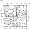
- Fig. 2 is an enlarged cross-sectional view of the fluorescent plate 1. Next, characteristic features of the fluorescent plate 1 of the present embodiment will be described. As shown in Fig. 2 , the fluorescent plate 1 has a fluorescent phase 10, a light-transmitting phase 20, and voids 30.
- the fluorescent phase 10 is formed of a plurality of fluorescent crystalline particles.
- the fluorescent crystalline particles have a composition represented by a chemical formula A 3 B 5 O 12 :Ce (i.e., a garnet-type crystal structure).
- the formula A 3 B 5 O 12 :Ce denotes that Ce forms a solid solution with A 3 B 5 O 12 , and element A is partially substituted by Ce.
- Each of element A and element B in the chemical formula A 3 B 5 O 12 :Ce represents at least one element selected from the corresponding element group:
- composition and element type of the fluorescent crystalline particles forming the fluorescent phase 10 are not limited to the aforementioned composition and types of elements.
- One single fluorescent phase 10 may be formed of fluorescent crystalline particles of a plurality of types.
- the light-transmitting phase 20 is formed of a plurality of light-transmitting crystalline particles.
- the light-transmitting crystalline particles have a composition represented by a chemical formula Al 2 O 3 .
- the light-transmitting phase 20 disposed in the fluorescent plate 1 allows passage of light and also serves as a heat transfer route which can efficiently transfer heat generated upon generation of fluorescence at the fluorescent phase 10 to the heat radiation member 7.
- the refractive index of the light-transmitting phase 20 is smaller than that of the fluorescent phase 10.
- the voids 30 are provided such that they are surrounded by the fluorescent phase 10 and the light-transmitting phase 20.
- the fluorescent plate 1 of the present embodiment is provided with a plurality of the voids 30.
- the void 30 refers to an area where neither the fluorescent phase 10 nor the light-transmitting phase 20 is present, as observed in a cross section of the fluorescent plate 1 shown in Fig. 2 . More specifically, it refers to a space having an equivalent circle diameter (i.e., a diameter of a perfect circle having an area equivalent to that of the cross-sectional area) of 0.4 micrometers or greater and 50 micrometers or smaller.
- the plurality of voids 30 have an average equivalent circle diameter of 1 micrometer or greater and smaller than 10 micrometers.
- the refractive index of the voids 30 is lower than that of the light-transmitting phase 20. In other words, the refractive index of the voids 30 is lower than that of the fluorescent phase 10.
- the portion of the fluorescent plate 1 other than voids 30 is formed of the fluorescent phase 10 at a volume ratio of 60% and the light-transmitting phase 20 at a volume ratio of 40%.
- the ratio of the area of the fluorescent phase 10 present in the fluorescent plate 1 to the total area of the fluorescent phase 10 and the light-transmitting phase 20 present in the fluorescent plate 1 is 60%
- the similar area ratio of the light-transmitting phase 20 is 40%. That is, in the cross section of the fluorescent plate 1 of the present embodiment, the area ratio of the fluorescent phase 10 is higher by 20% than that of the light-transmitting phase 20.
- the area ratio of the fluorescent phase 10 in a cross section of the fluorescent plate 1 is preferably 90% or lower. According to this feature, light is scattered in a suitable manner in the light-transmitting phase 20, and the optical path length in the fluorescent phase 10 is comparatively prolonged, whereby a drop in percent light absorption can be suppressed.
- Fig. 3 is an enlarged view of part A of Fig. 2 .
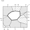
- Fig. 3 is a cross section of the fluorescent plate 1 including a typical void 30.
- the circumference 31 of the void 30 is in contact with the fluorescent phase 10 or the light-transmitting phase 20.
- the void 30 is surrounded by the fluorescent phase 10 and the light-transmitting phase 20, but the surface of the fluorescent phase 10 and that of the light-transmitting phase 20 are exposed to the void 30.
- the circumference 31 of the void 30 shown in Fig. 3 is denoted by a thicker line as compared with the contour line of the fluorescent phase 10 or the light-transmitting phase 20.
- the full length of the circumference 31 of the void 30 is represented by length L
- the length of a part 31a of the circumference 31 in contact with the fluorescent phase 10 i.e., a part represented by a dashed line put inside the circumference 31 in Fig. 3
- the ratio of the area of the fluorescent phase 10 present in the fluorescent plate 1 to the total area of the fluorescent phase 10 and the light-transmitting phase 20 present in the fluorescent plate 1 is represented by area ratio Rs.
- the ratio of the length La of a part of the circumference 31 in contact with the fluorescent phase 10 to the full length L of the circumference 31 (hereinafter, the ratio is referred to as a "circumference ratio"), and the area ratio Rs of the fluorescent plate 1 is represented by the following formula (1) .
- the circumference ratio La/L of the void 30 is about 0.75, and the area ratio Rs is 0.6.
- the circumference ratio La/L is greater by about 15% than the area ratio Rs, and the relationship (1) is satisfied. This feature indicates that a relatively large part of the surface of the fluorescent phase 10 is exposed to the void 30.
- the average ratio of a portion of the circumference 31 of a void 30, which portion is in contact with the fluorescent phase 10 to the entire circumference 31 of the void 30, is higher than the ratio of the area of the fluorescent phase 10 present in the fluorescent plate 1 to the total area of the fluorescent phase 10 and the light-transmitting phase 20 present in the fluorescent plate 1.
- the term "average ratio" refers to a value derived by dividing the sum of circumference ratios (La/L) of a plurality of voids 30 present in a cross section of the fluorescent plate 1 by the number of voids 30 included in the fluorescent plate 1. For example, in the cross section shown in Fig.
- the average ratio is calculated by dividing the sum of circumference ratios (La/L) of three voids 30 (except for the broken void 30 at a left corner) by 3 (i.e., the number of voids 30).
- a part of the circumference 31 in contact with the light-transmitting phase 20 i.e., a part represented by a dotted line put inside the circumference 31 in Fig. 3 ) is represented by reference numeral 31b.
- a method for producing the fluorescent plate 1 will be described.
- the method for producing the fluorescent plate 1 firstly, Y 2 O 3 , and CeO 2 which are weighed in advance, and a pore-forming material (e.g., acrylic beads) are added with pure water, and the mixture is kneaded and pulverized. The product is granulated by means of a spray dryer. Subsequently, Al 2 O 3 was added to the thus-granulated particles (i.e., powder) in such an amount that the ratio of the fluorescent phase is adjusted to 60 vol%. The resultant mixture is mixed with a specific amount of a binder and a specific amount of a pore-forming material.
- a pore-forming material e.g., acrylic beads
- the resultant mixture was kneaded under shear force, to thereby prepare a ceramic raw material.
- a portion of acrylic beads to be incorporated into the fluorescent plate 1 is added to Y 2 O 3 and other components, and the remaining portion of acrylic beads to be incorporated into the fluorescent plate 1 is added to the granulated powder, Al 2 O 3 , and other components.
- the thus-prepared ceramic raw material is formed into a sheet by means of an extruder, and the sheet is fired at 1,700 degrees Celsius in air for sintering, to thereby yield the fluorescent plate 1.
- a reflection member 6 in the form of a film is formed on the backside 1b of the fluorescent plate 1 through vapor deposition or sputtering of silver.
- gold-tin solder foil is sandwiched between the heat radiation member 7 and the reflection member 6 as film formed on the fluorescent plate 1, and the stacked body is heated in a reflow furnace under nitrogen or hydrogen.
- the fluorescent plate 1 is joined to the heat radiation member 7, whereby the wavelength conversion member 2 is yielded.
- joining of the fluorescent plate 1 to the heat radiation member 7 may be performed through application of a gold-tin solder paste.
- a light source 9 is set such that an incident surface 1a of the fluorescent plate 1 included in the wavelength conversion member 2 is irradiated with light, to thereby complete packaging of the wavelength conversion member 2 and the light source 9.
- the light source device 3 is fabricated.
- the fluorescent plate 1 of the present embodiment was assessed by some tests. The details of the tests and the results will be described.
- a plurality of fluorescent plate samples were prepared. Each sample was irradiated with light, and luminance was measured for each sample, to thereby assess the light extraction efficiency of the sample. The assessment was performed in terms of three characteristics: (i) circumferential ratio; (ii) equivalent circle diameter of voids, and (iii) area ratio.
- Each sample was ground to a thickness of 200 micrometers, and a surface of the sample was mirror-polished, to thereby prepare a luminance measurement sample.
- the luminance measurement sample was irradiated with laser light (wavelength: 450 nm, beam diameter: 0.4 mm, and output: 5 W). The luminance of the light toward the reflection direction was measured by means of a luminance meter.
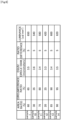
- Fig. 4 is a table showing the results of an assessment test on the circumferential ratio of the fluorescent plate of the first embodiment.
- Samples for assessment were prepared through a method almost equivalent to the aforementioned method for producing the fluorescent plate 1.
- the amount of pore-forming material mixed with Y 2 O 3 and CeO 2 which were weighed in advance was changed, and the remaining pore-forming material was added when Al 2 O 3 was added to the granulated powder, to thereby prepare a ceramic raw material.
- sample 1 firstly, a portion of acrylic beads (50% of the beads to be incorporated into sample 1) was mixed and pulverized with Y 2 O 3 and CeO 2 , and the product was granulated by means of a spray dryer.
- Sample 1 shown in the table of Fig. 4 was a sample having the same characteristics (area ratio, circumference ratio, and equivalent circle diameter of voids) as those of the fluorescent plate 1 of the present embodiment and employed as a reference sample in the assessment test. As shown in Fig. 4 , the test results have revealed that a higher luminance can be achieved as the difference between the circumference ratio and the area ratio (hereinafter referred to as a "ratio difference") increases. Particularly when the ratio difference was 3% or greater, a luminance of 500 cd/mm 2 was attained. Thus, the light extraction efficiency of the fluorescent plate was found to be enhanced.
- Fig. 5 is a table showing the results of an assessment test on the equivalent circle diameter of voids of the fluorescent plate of the first embodiment.
- Samples for assessment were prepared through a method almost equivalent to the aforementioned method for producing the fluorescent plate 1.
- the particle size of the pore-forming material mixed with Y 2 O 3 and CeO 2 which were weighed in advance and the particle size of the pore-forming material added to the granulated powder with Al 2 O 3 were changed.
- the test results have revealed that, when the equivalent circle diameter of voids was 3.5 micrometers, 4.6 micrometers, and 5.6 micrometers, the luminance was higher than 500 cd/mm 2 .
- sample 1 shown in the table of Fig. 5 is the same as sample 1 shown in Fig. 4 .
- Fig. 6 is a table showing the results of an assessment test on the area ratio of the fluorescent plate.
- Samples for assessment were prepared through a method almost equivalent to the aforementioned method for producing the fluorescent plate 1.
- the amounts of Y 2 O 3 and CeO 2 to which a pore-forming material and pure water were to be added were modified.
- the test results have revealed that, when the area ratio was 30% or greater and 90% or smaller (i.e., 30%, 60%, 75%, 85%, and 90%), a luminance of 500 cd/mm 2 or higher was achieved.
- the area ratio was 20%
- the luminance was found to be lower than 500 cd/mm 2 .
- sample 1 shown in the table of Fig. 6 is the same as sample 1 shown in Fig. 4 .
- the fluorescent plate 1 includes a plurality of voids 30 which are surrounded by the fluorescent phase 10 and the light-transmitting phase 20.
- the average ratio of a portion 31a of the circumference 31 of a void 30, which portion is in contact with the fluorescent phase 10 to the entire circumference of the void 30, is higher than the ratio of the area of the fluorescent phase 10 present in the fluorescent plate 1 to the total area of the fluorescent phase 10 and the light-transmitting phase 20 present in the fluorescent plate 1.
- This feature indicates that the fluorescent phase 10 is present around the voids 30 at a higher ratio than the compositional ratio of the fluorescent phase 10 to the entire fluorescent plate 1.
- the average ratio of the portion 31a of the circumference 31 of a void 30 in contact with the fluorescent phase 10 to the entire circumference 31 of the void 30 is higher, by 5% or more, than the ratio of the area of the fluorescent phase 10 present in the fluorescent plate 1 to the total area of the fluorescent phase 10 and the light-transmitting phase 20 present in the fluorescent plate 1. Accordingly, the fluorescent phase 10 is present around the voids 30 at a particularly high ratio.
- the light including the fluorescence emitted from the fluorescent phase 10 by the excitation light is more effectively reflected at the surface of the fluorescent phase 10 in the voids 30, and the quantity of light radiated to the outside of the fluorescent plate 1 can increase.
- light extraction efficiency can be further enhanced.
- the average equivalent circle diameter of the voids 30 is 1 micrometer or greater and smaller than 10 micrometers, which range corresponds to the wavelength of visible light or longer.
- the average equivalent circle diameter of the voids 30 is 1 micrometer or greater and smaller than 10 micrometers, which range corresponds to the wavelength of visible light or longer.
- the ratio of the area of the fluorescent phase 10 present in the fluorescent plate 1 to the total area of the fluorescent phase 10 and the light-transmitting phase 20 present in the fluorescent plate 1 is 60%, falling within a range of 21% or higher and 90% or lower.
- the average ratio of a portion 31a of the circumference 31 of a void 30, which portion is in contact with the fluorescent phase 10 to the entire circumference 31 of the void 30, can be regulated to such a level that the light extraction efficiency of the fluorescent plate 1 can be enhanced by an increase in reflection of light at the surface of the fluorescent phase 10 in the void 30.
- light is scattered in a suitable manner in the light-transmitting phase, and the optical path length in the fluorescent phase is comparatively prolonged, whereby a drop in percent light absorption can be suppressed.
- light extraction efficiency can be further enhanced.
- the wavelength conversion member 2 includes a reflection member 6 which reflects the fluorescence emitted from the fluorescent plate 1 and the excitation light.
- a reflection member 6 which reflects the fluorescence emitted from the fluorescent plate 1 and the excitation light.
- the configuration as shown in, for example, Fig. 1 , in the fluorescent plate 1, light radiating to a direction different from the direction of light L2 is reflected by the reflection member 6 toward the target direction. As a result, a large quantity of light can be radiated from the wavelength conversion member 2.
- the wavelength conversion member 2 possesses a heat radiation member 7 for dissipating heat of the fluorescent plate 1 to an outside atmosphere.
- heat generated at fluorescent emission induced by excitation light can be efficiently dissipated to an outside atmosphere, thereby suppressing quenching, which would otherwise be caused by a rise in temperature of the fluorescent plate 1.
- a drop in quantity of light radiated from the wavelength conversion member 2 can be suppressed.
- the light source device 3 has a light source 9 which radiates light L1 to the fluorescent plate 1.
- the light source 9 emits light L1 to the fluorescent plate 1
- fluorescence is generated in the fluorescent plate 1 by a certain light component of light L1.
- the fluorescence emitted by fluorescent plate 1 is reflected by the surface of the fluorescent phase 10 whose predominant portions face toward the voids 30, whereby the quantity of light radiated to the outside the fluorescent plate 1 increases.
- the light source device 3 can provide enhanced light emission intensity.
- one void 30 of the fluorescent plate 1 as shown in Fig. 3 had a circumference ratio La/L of about 0.75 and an area ratio Rs of 0.6.
- the ratio of the portion 31a of the circumference 31 in contact with the fluorescent phase 10 to the entire circumference 31 was higher, by 5% or more, than the ratio of the area of the fluorescent phase 10 present in the fluorescent plate 1 to the total area of the fluorescent phase 10 and the light-transmitting phase 20 present in the fluorescent plate 1.
- the difference between the ratio of the portion 31a of the circumference 31 in contact with the fluorescent phase 10 to the entire circumference 31 and the area ratio may be smaller than 5%. However, when the difference is greater, light is more effectively reflected at the surface of the fluorescent phase 10 in the voids 30, whereby the quantity of light radiated to the outside of the fluorescent plate 1 can increase.
- the average equivalent circle diameter of a plurality of voids 30 was adjusted to 1 micrometer or greater and smaller than 10 micrometers.
- the average equivalent circle diameter of a plurality of voids 30 may be smaller than 1 micrometer or 10 micrometers or greater.
- the average equivalent circle diameter of the voids 30 is adjusted to 1 micrometer or greater and smaller than 10 micrometers, which range corresponds to the wavelength of visible light or longer, visible light can be more effectively reflected at the surface of the fluorescent phase 10.
- the ratio of the area of the fluorescent phase 10 present in the fluorescent plate 1 to the total area of the fluorescent phase 10 and the light-transmitting phase 20 present in the fluorescent plate 1 was adjusted to 60%, but no particular limitation is imposed on the area ratio of the fluorescent phase 10 in the fluorescent plate 1.
- the area ratio of the fluorescent phase 10 is 21% or higher, the average ratio of the fluorescent phase 10 can be regulated to such a level that the light extraction efficiency of the fluorescent plate 1 can be enhanced by an increase in reflection of light at the surface of the fluorescent phase 10 in the void 30. Thus, light extraction efficiency can be enhanced.
- the area ratio of the fluorescent phase 10 is 90% or lower, light is scattered in a suitable manner in the light-transmitting phase, and the optical path length in the fluorescent phase is comparatively prolonged, whereby a drop in percent light absorption can be suppressed. Thus, light extraction efficiency can be enhanced.
- the light source device 3 is a reflection-type light source device.
- the fluorescent plate 1 may be applied to a transmission-type light source device.
- the portion of the fluorescent plate 1 other than voids 30 was formed of the fluorescent phase 10 at a volume ratio of 60% and the light-transmitting phase 20 at a volume ratio of 40%.
- the compositional ratio of the fluorescent plate 1 may be the fluorescent phase 10 at a volume ratio less than 100% and the light-transmitting phase 20 at a volume ratio less than 100%.
- the light-transmitting phase 20 allows passage of light in such a manner that the fluorescent phase 10 throughout the fluorescent plate 1 can emit fluorescence, and also serves as a heat conduction path for dissipating the heat generated in the fluorescent phase 10 to the outside atmosphere. Therefore, the compositional ratio of the light-transmitting phase 20 is preferably, for example, about 10%. When the ratio of the fluorescent phase 10 is 90% or higher, difficulty is encountered in controlling the circumference ratio.
Landscapes
- Engineering & Computer Science (AREA)
- General Engineering & Computer Science (AREA)
- Physics & Mathematics (AREA)
- Spectroscopy & Molecular Physics (AREA)
- Vessels And Coating Films For Discharge Lamps (AREA)
- Semiconductor Lasers (AREA)
- Optical Filters (AREA)
- Non-Portable Lighting Devices Or Systems Thereof (AREA)
- Formation Of Various Coating Films On Cathode Ray Tubes And Lamps (AREA)
- Led Device Packages (AREA)
- Planar Illumination Modules (AREA)
Abstract
Description
- The present invention relates to a fluorescent plate, to a wavelength conversion member, and to a light source device.
- Heretofore, there has been known a fluorescent plate (or screen) which emits fluorescence when being irradiated with light. In recent years, a number of known fluorescent plates have been highly-functionalized. Specifically, some fluorescent plates include a fluorescent phase which emits light having a wavelength different from that of the irradiation light, and a light-transmitting phase which allows passage of light. For example,
Patent Document 1 discloses a technique of providing a specific amount of voids surrounded by the fluorescent phase and the light-transmitting phase. - [Patent Document 1]
Japanese Patent No. 5989268 - However, for enhancing the light extraction efficiency of the fluorescent plate, there is still room for improvement in the aforementioned background technique. More specifically, when the technique disclosed in
Patent Document 1 is employed, the light emitted by the fluorescent phase is scattered in the voids, thereby often causing attenuation of the resultant light. Thus, the light extraction efficiency of the fluorescent plate may decrease. - Under such circumstances, an object of the present invention is to provide a technique for enhancing the light extraction efficiency of a fluorescent plate.
- The present invention has been accomplished so as to solve at least part of the above-described problem and can be realized in the following aspects.
- (1) In one aspect of the present invention, a fluorescent plate is provided. The fluorescent plate includes a fluorescent phase which emits fluorescence by excitation light, a light-transmitting phase which allows passage of the excitation light, and a plurality of voids surrounded by the fluorescent phase and the light-transmitting phase, wherein, in a cross section of the fluorescent plate including cross sections of the voids, an average ratio of a portion of the circumference of a void, which portion is in contact with the fluorescent phase to the entire circumference of the void, is higher than a ratio of the area of the fluorescent phase present in the fluorescent plate to the total area of the fluorescent phase and the light-transmitting phase present in the fluorescent plate.
According to the above configuration, the fluorescent plate includes a plurality of voids which are surrounded by the fluorescent phase and the light-transmitting phase. In a cross section of the fluorescent plate including cross sections of the voids, an average ratio of a portion of the circumference of a void, which portion is in contact with the fluorescent phase to the entire circumference of the void, is higher than a ratio of the area of the fluorescent phase present in the fluorescent plate to the total area of the fluorescent phase and the light-transmitting phase present in the fluorescent plate. This feature indicates that the fluorescent phase is present around the voids at a higher ratio than the compositional ratio of the fluorescent phase to the entire fluorescent plate. That is, a relatively large portion of the surface of the fluorescent phase is exposed to the voids. By virtue of this feature, total reflection of the light including the fluorescence emitted from the fluorescent phase by the excitation light is more effectively promoted at the surface of the fluorescent phase, which has a refractive index higher than that of the light-transmitting phase, in the voids, and the quantity of light radiated to the outside of the fluorescent plate can increase. Thus, light extraction efficiency can be enhanced. - (2) In the fluorescent plate of the above aspect, the ratio of the portion of the circumference of the void in contact with the fluorescent phase to the entire circumference of the void may be higher, by 5% or more, than the ratio of the area of the fluorescent phase present in the fluorescent plate to the total area of the fluorescent phase and the light-transmitting phase present in the fluorescent plate. According to this technical feature, in a cross section of the fluorescent plate including cross sections of the voids, the average ratio of the portion of the circumference of a void in contact with the fluorescent phase to the entire circumference of the void is higher, by 5% or more, than the ratio of the area of the fluorescent phase present in the fluorescent plate to the total area of the fluorescent phase and the light-transmitting phase present in the fluorescent plate. Accordingly, the fluorescent phase is present around the voids at a particularly high ratio. Therefore, the light including the fluorescence emitted from the fluorescent phase by the excitation light is more effectively reflected at the surface of the fluorescent phase in the voids, and the quantity of light radiated to the outside of the fluorescent plate can increase. Thus, light extraction efficiency can be further enhanced.
- (3) In the fluorescent plate of the above aspect, in a cross section of the fluorescent plate including cross sections of the voids, the plurality of voids may have an average diameter of 1 micrometer or greater and smaller than 10 micrometers. According to this technical feature, the average diameter of the voids is 1 micrometer or greater and smaller than 10 micrometers, which range corresponds to the wavelength of visible light or longer. As a result, passage of visible light included in the fluorescence through the voids is suppressed, and total reflection of visible light at the surface of the fluorescent phase in the voids can be promoted. Thus, the quantity of light radiated to the outside of the fluorescent plate can increase, and light extraction efficiency can be further enhanced.
- (4) In the fluorescent plate of the above aspect, in a cross section of the fluorescent plate including cross sections of the voids, a ratio of the area of the fluorescent phase present in the fluorescent plate to the total area of the fluorescent phase and the light-transmitting phase present in the fluorescent plate may be 21% or higher. According to this technical feature, in a cross section of the fluorescent plate including cross sections of the voids, the ratio of the area of the fluorescent phase present in the fluorescent plate to the total area of the fluorescent phase and the light-transmitting phase present in the fluorescent plate is 21% or higher. As a result, the average ratio of a portion of the circumference of a void, which portion is in contact with the fluorescent phase to the entire circumference of the void, can be regulated to such a level that the light extraction efficiency of the fluorescent plate can be enhanced by an increase in reflection of light at the surface of the fluorescent phase in the void. Thus, light extraction efficiency can be further enhanced.
- (5) In the fluorescent plate of the above aspect, in a cross section of the fluorescent plate including cross sections of the voids, a ratio of the area of the fluorescent phase present in the fluorescent plate to the total area of the fluorescent phase and the light-transmitting phase present in the fluorescent plate may be 90% or lower. According to this technical feature, light is scattered in a suitable manner in the light-transmitting phase, and the optical path length in the fluorescent phase is comparatively prolonged, whereby a drop in percent light absorption can be suppressed. Thus, light extraction efficiency can be enhanced.
- (6) In another aspect of the present invention, a wavelength conversion member is provided. The wavelength conversion member includes the fluorescent plate, and a reflection member which is attached to the fluorescent plate and which reflects the excitation light and the fluorescence. According to the configuration, the wavelength conversion member possesses a reflection member which reflects the fluorescence emitted from the fluorescent plate and the excitation light. Thus, in the fluorescent plate, light radiating to a direction different from the target direction of radiation is reflected by a reflection plate to the target direction. As a result, a large quantity of light can be radiated from the wavelength conversion member.
- (7) The wavelength conversion member of the above aspect may further include a heat radiation member for radiating heat of the fluorescent plate to an outside atmosphere. According to the configuration, the wavelength conversion member possesses a heat radiation member for dissipating heat of the fluorescent plate to an outside atmosphere. Thus, in the fluorescent plate, heat generated at fluorescent emission induced by excitation light can be efficiently dissipated to an outside atmosphere, thereby suppressing quenching, which would otherwise be caused by a rise in temperature of the fluorescent plate. As a result, a drop in quantity of light radiated from the wavelength conversion member can be suppressed.
- (8) In still another aspect of the present invention, a light source device is provided. The light source device may include the wavelength conversion member, and a light source which radiates the excitation light to the fluorescent plate. According to the configuration, the light source device possesses a light source which radiates the excitation light to the fluorescent plate. When the light source emits excitation light to the fluorescent plate, fluorescence occurs in the fluorescent plate by excitation light. The light including the resultant fluorescence is reflected by the surface of the fluorescent phase whose predominant portions face toward the voids, whereby the quantity of light radiated to the outside the fluorescent plate increases. As a result, the light source device can provide enhanced light emission intensity.
- Notably, the present invention can be realized in various modes. For example, the present invention may be realized as a method producing a fluorescent plate, a method for producing a wavelength conversion member, a method for producing a light source device, a system including a light source device, a method for regulating a light source device, a computer program for causing a manufacturing apparatus to execute manufacture of a light source device, and other modes.
-
- [
Fig. 1 ] Schematic view of a light source device having a fluorescent plate of a first embodiment. - [
Fig. 2 ] Enlarged cross-sectional view of the fluorescent plate. - [
Fig. 3 ] Enlarged view of part A ofFig. 2 . - [
Fig. 4 ] Table showing the results of an assessment test on the circumferential ratio of the fluorescent plate. - [
Fig. 5 ] Table showing the results of an assessment test on the equivalent circle diameter of voids in the fluorescent plate. - [
Fig. 6 ] Table showing the results of an assessment test on the area ratio of the fluorescent plate. -
Fig. 1 is a schematic view of alight source device 3 having afluorescent plate 1 of a first embodiment. When thefluorescent plate 1 of the present embodiment is irradiated with light L1 emitted by a light source 9 (e.g., a light emitting diode (LED) or a semiconductor laser (a laser diode (LD)) belonging to thelight source device 3, thefluorescent plate 1 generates florescence having a wavelength different from that of light L1. The fluorescence generated by thefluorescent plate 1 intermingles with light which has not been involved in generation of fluorescence at thefluorescent plate 1, to thereby provide radiation (light L2) toward a specific direction. As shown inFig. 1 , thelight source device 3 of the present embodiment is a reflection-type light source device and is used in various types of optical apparatuses such as headlights, lighting equipment, and projectors. Thelight source device 3 has the aforementionedlight source 9 and awavelength conversion member 2. Thewavelength conversion member 2 includes thefluorescent plate 1, areflection member 6, aheat radiation member 7, and ajoint layer 8. For the purpose of illustration, the members are illustrated inFig. 1 in such a manner that the dimensional relation differs from the actual relation. - The
fluorescent plate 1 is a plate-shape member formed of a sintered ceramic material. Thefluorescent plate 1 has anincident surface 1a into which the incident light L1 enters, and abackside surface 1b opposite to theincident surface 1a. Thefluorescent plate 1 generates fluorescence by the excitation light L1 which enters through theincident surface 1a. During generation of fluorescence, thefluorescent plate 1 generates heat. Detailed description of thefluorescent plate 1 will next be provided. - The
reflection member 6 is a thin film mainly formed of silver (Ag) and disposed on thebackside surface 1b of thefluorescent plate 1. Thereflection member 6 reflects, toward the direction of theincident surface 1a, the light passing throughfluorescent plate 1 of the light L1 emitted from thelight source 9, and the fluorescence going to thebackside surface 1b of the fluorescence generated by thefluorescent plate 1. Notably, thereflection member 6 may be formed of a material having high reflectivity such as silver alloy or aluminum (Al). - The
heat radiation member 7 is a plate-shape member formed of a material having a thermal conductivity higher than that of thefluorescent plate 1, such as copper, copper-molybdenum alloy, copper-tungsten alloy, aluminum, or aluminum nitride. Theheat radiation member 7 can dissipate heat of thefluorescent plate 1 transferred through thejoint layer 8 to an outside atmosphere. Notably, theheat radiation member 7 may be a single-layer member formed of any of the aforementioned materials, or a multi-layer member formed of materials which are identical to or different from one another. In addition, a metal film may be disposed on afluorescent plate 1side surface 7a of theheat radiation member 7 so as to enhance adhesion with thejoint layer 8. - The
joint layer 8 is disposed between thereflection member 6 and theheat radiation member 7 and is formed of gold (Au) and tin (Sn). Thejoint layer 8 can join thefluorescent plate 1 to theheat radiation member 7 and transfers the heat generated at thefluorescent plate 1 to theheat radiation member 7. Notably, thejoint layer 8 may be formed of a material other than gold and tin, and may be formed of a solder of other metals, or a sintered material of a micropowder of, for example, silver or copper (Cu). -
Fig. 2 is an enlarged cross-sectional view of thefluorescent plate 1. Next, characteristic features of thefluorescent plate 1 of the present embodiment will be described. As shown inFig. 2 , thefluorescent plate 1 has afluorescent phase 10, a light-transmittingphase 20, and voids 30. - The
fluorescent phase 10 is formed of a plurality of fluorescent crystalline particles. In the present embodiment, the fluorescent crystalline particles have a composition represented by a chemical formula A3B5O12:Ce (i.e., a garnet-type crystal structure). The formula A3B5O12:Ce denotes that Ce forms a solid solution with A3B5O12, and element A is partially substituted by Ce. Each of element A and element B in the chemical formula A3B5O12:Ce represents at least one element selected from the corresponding element group: - element A: Sc, Y, and lanthanoids (except for Ce) (however, element A may further include Gd); and
- element B; Al (element B may further include Ga).
- Notably, the composition and element type of the fluorescent crystalline particles forming the
fluorescent phase 10 are not limited to the aforementioned composition and types of elements. Onesingle fluorescent phase 10 may be formed of fluorescent crystalline particles of a plurality of types. - The light-transmitting
phase 20 is formed of a plurality of light-transmitting crystalline particles. The light-transmitting crystalline particles have a composition represented by a chemical formula Al2O3. The light-transmittingphase 20 disposed in thefluorescent plate 1 allows passage of light and also serves as a heat transfer route which can efficiently transfer heat generated upon generation of fluorescence at thefluorescent phase 10 to theheat radiation member 7. The refractive index of the light-transmittingphase 20 is smaller than that of thefluorescent phase 10. - The
voids 30 are provided such that they are surrounded by thefluorescent phase 10 and the light-transmittingphase 20. As shown inFig. 2 , thefluorescent plate 1 of the present embodiment is provided with a plurality of thevoids 30. In the present embodiment, the void 30 refers to an area where neither thefluorescent phase 10 nor the light-transmittingphase 20 is present, as observed in a cross section of thefluorescent plate 1 shown inFig. 2 . More specifically, it refers to a space having an equivalent circle diameter (i.e., a diameter of a perfect circle having an area equivalent to that of the cross-sectional area) of 0.4 micrometers or greater and 50 micrometers or smaller. In the present embodiment, the plurality ofvoids 30 have an average equivalent circle diameter of 1 micrometer or greater and smaller than 10 micrometers. The refractive index of thevoids 30 is lower than that of the light-transmittingphase 20. In other words, the refractive index of thevoids 30 is lower than that of thefluorescent phase 10. - In the present embodiment, the portion of the
fluorescent plate 1 other thanvoids 30 is formed of thefluorescent phase 10 at a volume ratio of 60% and the light-transmittingphase 20 at a volume ratio of 40%. In other words, in the cross section of thefluorescent plate 1 as shown inFig. 2 , the ratio of the area of thefluorescent phase 10 present in thefluorescent plate 1 to the total area of thefluorescent phase 10 and the light-transmittingphase 20 present in thefluorescent plate 1 is 60%, and the similar area ratio of the light-transmittingphase 20 is 40%. That is, in the cross section of thefluorescent plate 1 of the present embodiment, the area ratio of thefluorescent phase 10 is higher by 20% than that of the light-transmittingphase 20. The area ratio of thefluorescent phase 10 in a cross section of thefluorescent plate 1 is preferably 90% or lower. According to this feature, light is scattered in a suitable manner in the light-transmittingphase 20, and the optical path length in thefluorescent phase 10 is comparatively prolonged, whereby a drop in percent light absorption can be suppressed. -
Fig. 3 is an enlarged view of part A ofFig. 2 .Fig. 3 is a cross section of thefluorescent plate 1 including atypical void 30. As shown inFig. 3 , in thefluorescent plate 1 of the present embodiment, the circumference 31 of the void 30 is in contact with thefluorescent phase 10 or the light-transmittingphase 20. In other words, the void 30 is surrounded by thefluorescent phase 10 and the light-transmittingphase 20, but the surface of thefluorescent phase 10 and that of the light-transmittingphase 20 are exposed to the void 30. Notably, for the purpose of better illustration, the circumference 31 of the void 30 shown inFig. 3 is denoted by a thicker line as compared with the contour line of thefluorescent phase 10 or the light-transmittingphase 20. - In the void 30 shown in
Fig. 3 , the full length of the circumference 31 of the void 30 is represented by length L, and the length of apart 31a of the circumference 31 in contact with the fluorescent phase 10 (i.e., a part represented by a dashed line put inside the circumference 31 inFig. 3 ) is represented by length La. Also, the ratio of the area of thefluorescent phase 10 present in thefluorescent plate 1 to the total area of thefluorescent phase 10 and the light-transmittingphase 20 present in thefluorescent plate 1 is represented by area ratio Rs. In asingle void 30, the relationship between the ratio of the length La of a part of the circumference 31 in contact with thefluorescent phase 10 to the full length L of the circumference 31 (hereinafter, the ratio is referred to as a "circumference ratio"), and the area ratio Rs of thefluorescent plate 1 is represented by the following formula (1) .
- In a case shown in
Fig. 3 , the circumference ratio La/L of the void 30 is about 0.75, and the area ratio Rs is 0.6. Thus, the circumference ratio La/L is greater by about 15% than the area ratio Rs, and the relationship (1) is satisfied. This feature indicates that a relatively large part of the surface of thefluorescent phase 10 is exposed to the void 30. According to the present embodiment, in a cross section of thefluorescent plate 1 including cross sections ofvoids 30, the average ratio of a portion of the circumference 31 of a void 30, which portion is in contact with thefluorescent phase 10 to the entire circumference 31 of the void 30, is higher than the ratio of the area of thefluorescent phase 10 present in thefluorescent plate 1 to the total area of thefluorescent phase 10 and the light-transmittingphase 20 present in thefluorescent plate 1. The term "average ratio" refers to a value derived by dividing the sum of circumference ratios (La/L) of a plurality ofvoids 30 present in a cross section of thefluorescent plate 1 by the number ofvoids 30 included in thefluorescent plate 1. For example, in the cross section shown inFig. 2 , the average ratio is calculated by dividing the sum of circumference ratios (La/L) of three voids 30 (except for thebroken void 30 at a left corner) by 3 (i.e., the number of voids 30). Notably, a part of the circumference 31 in contact with the light-transmitting phase 20 (i.e., a part represented by a dotted line put inside the circumference 31 inFig. 3 ) is represented byreference numeral 31b. - Next, a method for producing the
fluorescent plate 1 will be described. In the method for producing thefluorescent plate 1, firstly, Y2O3, and CeO2 which are weighed in advance, and a pore-forming material (e.g., acrylic beads) are added with pure water, and the mixture is kneaded and pulverized. The product is granulated by means of a spray dryer. Subsequently, Al2O3 was added to the thus-granulated particles (i.e., powder) in such an amount that the ratio of the fluorescent phase is adjusted to 60 vol%. The resultant mixture is mixed with a specific amount of a binder and a specific amount of a pore-forming material. The resultant mixture was kneaded under shear force, to thereby prepare a ceramic raw material. In the preparation of the ceramic raw material, a portion of acrylic beads to be incorporated into thefluorescent plate 1 is added to Y2O3 and other components, and the remaining portion of acrylic beads to be incorporated into thefluorescent plate 1 is added to the granulated powder, Al2O3, and other components. The thus-prepared ceramic raw material is formed into a sheet by means of an extruder, and the sheet is fired at 1,700 degrees Celsius in air for sintering, to thereby yield thefluorescent plate 1. - In the production of a
wavelength conversion member 2 including thefluorescent plate 1, areflection member 6 in the form of a film is formed on thebackside 1b of thefluorescent plate 1 through vapor deposition or sputtering of silver. Subsequently, gold-tin solder foil is sandwiched between theheat radiation member 7 and thereflection member 6 as film formed on thefluorescent plate 1, and the stacked body is heated in a reflow furnace under nitrogen or hydrogen. As a result, thefluorescent plate 1 is joined to theheat radiation member 7, whereby thewavelength conversion member 2 is yielded. Notably, instead of use of gold-tin solder foil, joining of thefluorescent plate 1 to theheat radiation member 7 may be performed through application of a gold-tin solder paste. - Further, in the production of a
light source device 3 including thewavelength conversion member 2, alight source 9 is set such that anincident surface 1a of thefluorescent plate 1 included in thewavelength conversion member 2 is irradiated with light, to thereby complete packaging of thewavelength conversion member 2 and thelight source 9. Thus, thelight source device 3 is fabricated. - Next, the
fluorescent plate 1 of the present embodiment was assessed by some tests. The details of the tests and the results will be described. In the assessment, a plurality of fluorescent plate samples were prepared. Each sample was irradiated with light, and luminance was measured for each sample, to thereby assess the light extraction efficiency of the sample. The assessment was performed in terms of three characteristics: (i) circumferential ratio; (ii) equivalent circle diameter of voids, and (iii) area ratio. - In the present assessment test, the aforementioned three characteristics were determined through the following methods.
- Each sample was cut, and the cut surface was mirror-polished. The thus-provided surface was observed under an FE-SEM. In image analysis by use of winloof, a cross-sectional image was taken at five points selected at random. The full length of the circumference of each void, the length of a part of the circumference in contact with the fluorescent phase, and the length of a part of the circumference in contact with the light-transmitting phase were determined. Based on the obtained data, the circumference ratio (i.e., the ratio of the length of a part of the circumference in contact with the fluorescent phase to the full length of the circumference of the void) was calculated. The equivalent circle diameter of voids was calculated by use of winloof.
- Each sample was ground to a thickness of 200 micrometers, and a surface of the sample was mirror-polished, to thereby prepare a luminance measurement sample. The luminance measurement sample was irradiated with laser light (wavelength: 450 nm, beam diameter: 0.4 mm, and output: 5 W). The luminance of the light toward the reflection direction was measured by means of a luminance meter.
-
Fig. 4 is a table showing the results of an assessment test on the circumferential ratio of the fluorescent plate of the first embodiment. Samples for assessment were prepared through a method almost equivalent to the aforementioned method for producing thefluorescent plate 1. In a specific sample preparation procedure, the amount of pore-forming material mixed with Y2O3 and CeO2 which were weighed in advance was changed, and the remaining pore-forming material was added when Al2O3 was added to the granulated powder, to thereby prepare a ceramic raw material. In the case ofsample 1, firstly, a portion of acrylic beads (50% of the beads to be incorporated into sample 1) was mixed and pulverized with Y2O3 and CeO2, and the product was granulated by means of a spray dryer. To the granulated powder, the remaining 50% of acrylic beads and Al2O3 were added, to thereby prepare a ceramic raw material. Other samples were prepared in the same manner, except that the ratio of the amount of the first addition of acrylic beads to that of the second addition thereof was varied, to thereby modify the circumference ratio of the fluorescent plate.Sample 1 shown in the table ofFig. 4 was a sample having the same characteristics (area ratio, circumference ratio, and equivalent circle diameter of voids) as those of thefluorescent plate 1 of the present embodiment and employed as a reference sample in the assessment test. As shown inFig. 4 , the test results have revealed that a higher luminance can be achieved as the difference between the circumference ratio and the area ratio (hereinafter referred to as a "ratio difference") increases. Particularly when the ratio difference was 3% or greater, a luminance of 500 cd/mm2 was attained. Thus, the light extraction efficiency of the fluorescent plate was found to be enhanced. -
Fig. 5 is a table showing the results of an assessment test on the equivalent circle diameter of voids of the fluorescent plate of the first embodiment. Samples for assessment were prepared through a method almost equivalent to the aforementioned method for producing thefluorescent plate 1. In a specific sample preparation procedure, the particle size of the pore-forming material mixed with Y2O3 and CeO2 which were weighed in advance and the particle size of the pore-forming material added to the granulated powder with Al2O3 were changed. As is clear fromFig. 5 , the test results have revealed that, when the equivalent circle diameter of voids was 3.5 micrometers, 4.6 micrometers, and 5.6 micrometers, the luminance was higher than 500 cd/mm2. In contrast, when the equivalent circle diameter of voids was 1.0 micrometers and 10 micrometers, the luminance was found to be lower than 500 cd/mm2. Thus, when the equivalent circle diameter of voids was greater than 1.0 micrometer and smaller than 10 micrometers, a higher luminance was found to be achieved. Notably,sample 1 shown in the table ofFig. 5 is the same assample 1 shown inFig. 4 . -
Fig. 6 is a table showing the results of an assessment test on the area ratio of the fluorescent plate. Samples for assessment were prepared through a method almost equivalent to the aforementioned method for producing thefluorescent plate 1. In a specific sample preparation procedure, the amounts of Y2O3 and CeO2 to which a pore-forming material and pure water were to be added were modified. As is clear fromFig. 6 , the test results have revealed that, when the area ratio was 30% or greater and 90% or smaller (i.e., 30%, 60%, 75%, 85%, and 90%), a luminance of 500 cd/mm2 or higher was achieved. In contrast, when the area ratio was 20%, the luminance was found to be lower than 500 cd/mm2. Notably,sample 1 shown in the table ofFig. 6 is the same assample 1 shown inFig. 4 . - According to the aforementioned
fluorescent plate 1 of the present embodiment, thefluorescent plate 1 includes a plurality ofvoids 30 which are surrounded by thefluorescent phase 10 and the light-transmittingphase 20. In a cross section of thefluorescent plate 1 including cross sections of thevoids 30, the average ratio of aportion 31a of the circumference 31 of a void 30, which portion is in contact with thefluorescent phase 10 to the entire circumference of the void 30, is higher than the ratio of the area of thefluorescent phase 10 present in thefluorescent plate 1 to the total area of thefluorescent phase 10 and the light-transmittingphase 20 present in thefluorescent plate 1. This feature indicates that thefluorescent phase 10 is present around thevoids 30 at a higher ratio than the compositional ratio of thefluorescent phase 10 to the entirefluorescent plate 1. That is, a relatively large portion of the surface of thefluorescent phase 10 is exposed to thevoids 30. By virtue of this feature, total reflection of the light including the fluorescence emitted from thefluorescent phase 10 by the excitation light is more effectively promoted at the surface of thefluorescent phase 10, which has a refractive index higher than that of the light-transmittingphase 20, in thevoids 30, and the quantity of light radiated to the outside of thefluorescent plate 1 can increase. Thus, light extraction efficiency can be enhanced. - According to the
fluorescent plate 1 of the present embodiment, in a cross section of thefluorescent plate 1 including cross sections of thevoids 30, the average ratio of theportion 31a of the circumference 31 of a void 30 in contact with thefluorescent phase 10 to the entire circumference 31 of the void 30 is higher, by 5% or more, than the ratio of the area of thefluorescent phase 10 present in thefluorescent plate 1 to the total area of thefluorescent phase 10 and the light-transmittingphase 20 present in thefluorescent plate 1. Accordingly, thefluorescent phase 10 is present around thevoids 30 at a particularly high ratio. Therefore, the light including the fluorescence emitted from thefluorescent phase 10 by the excitation light is more effectively reflected at the surface of thefluorescent phase 10 in thevoids 30, and the quantity of light radiated to the outside of thefluorescent plate 1 can increase. Thus, light extraction efficiency can be further enhanced. - According to the
fluorescent plate 1 of the present embodiment, the average equivalent circle diameter of thevoids 30 is 1 micrometer or greater and smaller than 10 micrometers, which range corresponds to the wavelength of visible light or longer. As a result, passage of visible light included in the fluorescence through thevoids 30 is suppressed, and total reflection of visible light at the surface of thefluorescent phase 10 in thevoids 30 can be promoted. Thus, the quantity of light radiated to the outside of thefluorescent plate 1 can increase, and light extraction efficiency can be further enhanced. - According to the
fluorescent plate 1 of the present embodiment, in a cross section of thefluorescent plate 1 including cross sections of thevoids 30, the ratio of the area of thefluorescent phase 10 present in thefluorescent plate 1 to the total area of thefluorescent phase 10 and the light-transmittingphase 20 present in thefluorescent plate 1 is 60%, falling within a range of 21% or higher and 90% or lower. As a result, the average ratio of aportion 31a of the circumference 31 of a void 30, which portion is in contact with thefluorescent phase 10 to the entire circumference 31 of the void 30, can be regulated to such a level that the light extraction efficiency of thefluorescent plate 1 can be enhanced by an increase in reflection of light at the surface of thefluorescent phase 10 in thevoid 30. Also, light is scattered in a suitable manner in the light-transmitting phase, and the optical path length in the fluorescent phase is comparatively prolonged, whereby a drop in percent light absorption can be suppressed. Thus, light extraction efficiency can be further enhanced. - According to the
wavelength conversion member 2 of the present embodiment, thewavelength conversion member 2 includes areflection member 6 which reflects the fluorescence emitted from thefluorescent plate 1 and the excitation light. According to the configuration, as shown in, for example,Fig. 1 , in thefluorescent plate 1, light radiating to a direction different from the direction of light L2 is reflected by thereflection member 6 toward the target direction. As a result, a large quantity of light can be radiated from thewavelength conversion member 2. - According to the
wavelength conversion member 2 of the present embodiment, thewavelength conversion member 2 possesses aheat radiation member 7 for dissipating heat of thefluorescent plate 1 to an outside atmosphere. Thus, in thefluorescent plate 1, heat generated at fluorescent emission induced by excitation light can be efficiently dissipated to an outside atmosphere, thereby suppressing quenching, which would otherwise be caused by a rise in temperature of thefluorescent plate 1. As a result, a drop in quantity of light radiated from thewavelength conversion member 2 can be suppressed. - According to the
light source device 3 of the present embodiment, thelight source device 3 has alight source 9 which radiates light L1 to thefluorescent plate 1. When thelight source 9 emits light L1 to thefluorescent plate 1, fluorescence is generated in thefluorescent plate 1 by a certain light component of light L1. The fluorescence emitted byfluorescent plate 1 is reflected by the surface of thefluorescent phase 10 whose predominant portions face toward thevoids 30, whereby the quantity of light radiated to the outside thefluorescent plate 1 increases. As a result, thelight source device 3 can provide enhanced light emission intensity. - The present invention is not limited to the above-described embodiment and can be practiced in various forms without departing from the gist of the invention, and, for example, the following modifications are possible.
- In the aforementioned embodiment, one
void 30 of thefluorescent plate 1 as shown inFig. 3 had a circumference ratio La/L of about 0.75 and an area ratio Rs of 0.6. Thus, the ratio of theportion 31a of the circumference 31 in contact with thefluorescent phase 10 to the entire circumference 31 was higher, by 5% or more, than the ratio of the area of thefluorescent phase 10 present in thefluorescent plate 1 to the total area of thefluorescent phase 10 and the light-transmittingphase 20 present in thefluorescent plate 1. The difference between the ratio of theportion 31a of the circumference 31 in contact with thefluorescent phase 10 to the entire circumference 31 and the area ratio may be smaller than 5%. However, when the difference is greater, light is more effectively reflected at the surface of thefluorescent phase 10 in thevoids 30, whereby the quantity of light radiated to the outside of thefluorescent plate 1 can increase. - In the aforementioned embodiment, the average equivalent circle diameter of a plurality of
voids 30 was adjusted to 1 micrometer or greater and smaller than 10 micrometers. The average equivalent circle diameter of a plurality ofvoids 30 may be smaller than 1 micrometer or 10 micrometers or greater. However, when the average equivalent circle diameter of thevoids 30 is adjusted to 1 micrometer or greater and smaller than 10 micrometers, which range corresponds to the wavelength of visible light or longer, visible light can be more effectively reflected at the surface of thefluorescent phase 10. - In the aforementioned embodiment, in a cross section of the
fluorescent plate 1, the ratio of the area of thefluorescent phase 10 present in thefluorescent plate 1 to the total area of thefluorescent phase 10 and the light-transmittingphase 20 present in thefluorescent plate 1 was adjusted to 60%, but no particular limitation is imposed on the area ratio of thefluorescent phase 10 in thefluorescent plate 1. When the area ratio of thefluorescent phase 10 is 21% or higher, the average ratio of thefluorescent phase 10 can be regulated to such a level that the light extraction efficiency of thefluorescent plate 1 can be enhanced by an increase in reflection of light at the surface of thefluorescent phase 10 in thevoid 30. Thus, light extraction efficiency can be enhanced. Also, when the area ratio of thefluorescent phase 10 is 90% or lower, light is scattered in a suitable manner in the light-transmitting phase, and the optical path length in the fluorescent phase is comparatively prolonged, whereby a drop in percent light absorption can be suppressed. Thus, light extraction efficiency can be enhanced. - According to the aforementioned embodiment, the
light source device 3 is a reflection-type light source device. However, thefluorescent plate 1 may be applied to a transmission-type light source device. - In the aforementioned embodiment, the portion of the
fluorescent plate 1 other thanvoids 30 was formed of thefluorescent phase 10 at a volume ratio of 60% and the light-transmittingphase 20 at a volume ratio of 40%. However, the compositional ratio of thefluorescent plate 1 may be thefluorescent phase 10 at a volume ratio less than 100% and the light-transmittingphase 20 at a volume ratio less than 100%. In thefluorescent plate 1, the light-transmittingphase 20 allows passage of light in such a manner that thefluorescent phase 10 throughout thefluorescent plate 1 can emit fluorescence, and also serves as a heat conduction path for dissipating the heat generated in thefluorescent phase 10 to the outside atmosphere. Therefore, the compositional ratio of the light-transmittingphase 20 is preferably, for example, about 10%. When the ratio of thefluorescent phase 10 is 90% or higher, difficulty is encountered in controlling the circumference ratio. - Although the present aspects have been described on the basis of embodiments and modifications, the above-described embodiments of the aspects is provided so as to facilitate the understanding of the present aspects and does not limit the present aspect. The present aspects can be changed or improved without departing from the purpose of the aspects and the claims, and encompasses equivalents thereof. Also, the technical feature(s) may be eliminated as appropriate unless the present specification mentions that the technical feature(s) is mandatory.
-
- 1: fluorescent plate
- 2: wavelength conversion member
- 3: light source device
- 6: reflection member
- 7: heat radiation member
- 9: light source
- 10: fluorescent phase
- 20: light-transmitting phase
- 30: void
- 31: circumference
- 31a: portion in contact with fluorescent phase
- L1: excitation light
- L2: radiation light
- Rs: area ratio
Claims (8)
- A fluorescent plate, characterized by comprisinga fluorescent phase which emits fluorescence by excitation light,a light-transmitting phase which allows passage of the excitation light, anda plurality of voids surrounded by the fluorescent phase and the light-transmitting phase,wherein, in a cross section of the fluorescent plate including cross sections of the voids, an average ratio of a portion of the circumference of a void, which portion is in contact with the fluorescent phase to the entire circumference of the void, is higher thana ratio of the area of the fluorescent phase present in the fluorescent plate to the total area of the fluorescent phase and the light-transmitting phase present in the fluorescent plate.
- The fluorescent plate according to claim 1,
wherein the ratio of the portion of the circumference of the void in contact with the fluorescent phase to the entire circumference of the void is higher, by 5% or more, than the ratio of the area of the fluorescent phase present in the fluorescent plate to the total area of the fluorescent phase and the light-transmitting phase present in the fluorescent plate. - The fluorescent plate according to claim 1 or 2,
wherein, in a cross section of the fluorescent plate including cross sections of the voids, the plurality of voids have an average diameter of 1 micrometer or greater and smaller than 10 micrometers. - The fluorescent plate according to any one of claims 1 to 3,
wherein, in a cross section of the fluorescent plate including cross sections of the voids, a ratio of the area of the fluorescent phase present in the fluorescent plate to the total area of the fluorescent phase and the light-transmitting phase present in the fluorescent plate is 21% or higher. - The fluorescent plate according to any one of claims 1 to 4,
wherein, in a cross section of the fluorescent plate including cross sections of the voids, a ratio of the area of the fluorescent phase present in the fluorescent plate to the total area of the fluorescent phase and the light-transmitting phase present in the fluorescent plate is 90% or lower. - A wavelength conversion member characterized by comprisinga fluorescent plate as recited in any one of claims 1 to 5, anda reflection member which is attached to the fluorescent plate and which reflects the excitation light and the fluorescence.
- The wavelength conversion member according to claim 6, further comprising a heat radiation member for radiating heat of the fluorescent plate to an outside atmosphere.
- A light source device characterized by comprisinga wavelength conversion member as recited in claim 6 or 7, anda light source which radiates the excitation light to the fluorescent plate.
Applications Claiming Priority (2)
| Application Number | Priority Date | Filing Date | Title |
|---|---|---|---|
| JP2020099394 | 2020-06-08 | ||
| PCT/JP2021/021144 WO2021251251A1 (en) | 2020-06-08 | 2021-06-03 | Fluorescent plate, wavelength conversion member, and light source device |
Publications (2)
| Publication Number | Publication Date |
|---|---|
| EP4163542A1 true EP4163542A1 (en) | 2023-04-12 |
| EP4163542A4 EP4163542A4 (en) | 2024-07-03 |
Family
ID=78846193
Family Applications (1)
| Application Number | Title | Priority Date | Filing Date |
|---|---|---|---|
| EP21823123.1A Pending EP4163542A4 (en) | 2020-06-08 | 2021-06-03 | FLUORESCENCE PLATE, WAVELENGTH CONVERSION ELEMENT AND LIGHT SOURCE DEVICE |
Country Status (7)
| Country | Link |
|---|---|
| US (1) | US11796156B2 (en) |
| EP (1) | EP4163542A4 (en) |
| JP (1) | JP7219855B2 (en) |
| KR (1) | KR102665901B1 (en) |
| CN (1) | CN114981593B (en) |
| TW (1) | TWI802898B (en) |
| WO (1) | WO2021251251A1 (en) |
Family Cites Families (24)
| Publication number | Priority date | Publication date | Assignee | Title |
|---|---|---|---|---|
| JPS5989268A (en) | 1982-11-10 | 1984-05-23 | Fuji Heavy Ind Ltd | Control valve device for power steering device |
| JPS5989268U (en) | 1982-12-08 | 1984-06-16 | 横河電機株式会社 | Optical/electrical measurement circuit |
| JP2000243302A (en) * | 1998-05-20 | 2000-09-08 | Mitsubishi Materials Corp | Phosphor film structure, paste for forming this phosphor film, and plasma display panel using this phosphor film |
| JP5271523B2 (en) * | 2007-09-28 | 2013-08-21 | 岡谷電機産業株式会社 | Method for producing fluorescent material carrier |
| TWI538262B (en) * | 2011-08-19 | 2016-06-11 | 晶元光電股份有限公司 | Wavelength Conversion Structure and Lighting Emitting Device including the Wavelength Conversion Structure |
| JP6413673B2 (en) * | 2014-11-13 | 2018-10-31 | ウシオ電機株式会社 | Fluorescent light source device |
| JP5989268B2 (en) | 2015-02-18 | 2016-09-07 | 日東電工株式会社 | Phosphor ceramics, sealed optical semiconductor element, circuit board, optical semiconductor device, and light emitting device |
| JP2017028251A (en) * | 2015-07-23 | 2017-02-02 | パナソニックIpマネジメント株式会社 | Wavelength conversion member, light source device, illumination device vehicle and method of manufacturing wavelength conversion member |
| JP6631084B2 (en) * | 2015-08-19 | 2020-01-15 | セイコーエプソン株式会社 | Method for manufacturing wavelength conversion element, wavelength conversion element, lighting device, and projector |
| CN106896632A (en) * | 2015-12-03 | 2017-06-27 | 精工爱普生株式会社 | Fluorophor, Wavelength changing element, light supply apparatus and projecting apparatus |
| EP3430309B1 (en) * | 2016-03-15 | 2020-05-06 | Signify Holding B.V. | A light emitting device |
| EP3534193B1 (en) * | 2016-10-28 | 2021-12-22 | Ngk Spark Plug Co., Ltd. | Optical wavelength conversion member and light-emitting device |
| JP6938938B2 (en) * | 2017-02-13 | 2021-09-22 | セイコーエプソン株式会社 | Wavelength converter, light source device and projector |
| WO2018154868A1 (en) * | 2017-02-27 | 2018-08-30 | パナソニックIpマネジメント株式会社 | Wavelength conversion member |
| JP2019015848A (en) * | 2017-07-06 | 2019-01-31 | 株式会社タムラ製作所 | Wavelength conversion member and method for manufacturing the same |
| JP6627914B2 (en) * | 2017-08-31 | 2020-01-08 | 日亜化学工業株式会社 | Fluorescent member, optical component, and light emitting device |
| JP2021028352A (en) * | 2017-12-05 | 2021-02-25 | シャープ株式会社 | Phosphor layer composition, phosphor member, light source device, and projection device |
| JP7115888B2 (en) * | 2018-04-02 | 2022-08-09 | 日本特殊陶業株式会社 | Optical wavelength conversion member and light emitting device |
| JP7068040B2 (en) * | 2018-05-28 | 2022-05-16 | 日本特殊陶業株式会社 | Optical wavelength converter |
| JP7119600B2 (en) * | 2018-06-06 | 2022-08-17 | ウシオ電機株式会社 | fluorescent light emitting element |
| JP7148291B2 (en) * | 2018-06-25 | 2022-10-05 | 日本特殊陶業株式会社 | Optical wavelength converter |
| CN110903088B (en) * | 2018-09-14 | 2022-02-22 | 深圳光峰科技股份有限公司 | Porous fluorescent ceramic and preparation method thereof, light-emitting device and projection device |
| JP2022041435A (en) * | 2020-09-01 | 2022-03-11 | キヤノン株式会社 | Wavelength conversion element, light source device, and image projection device |
| US12284850B2 (en) * | 2020-12-01 | 2025-04-22 | Lumileds Llc | Laterally heterogenous wavelength-converting layer |
-
2021
- 2021-06-03 KR KR1020227019924A patent/KR102665901B1/en active Active
- 2021-06-03 CN CN202180008269.2A patent/CN114981593B/en active Active
- 2021-06-03 EP EP21823123.1A patent/EP4163542A4/en active Pending
- 2021-06-03 WO PCT/JP2021/021144 patent/WO2021251251A1/en not_active Ceased
- 2021-06-03 US US18/000,864 patent/US11796156B2/en active Active
- 2021-06-03 TW TW110120163A patent/TWI802898B/en active
- 2021-06-03 JP JP2022530512A patent/JP7219855B2/en active Active
Also Published As
| Publication number | Publication date |
|---|---|
| TW202207482A (en) | 2022-02-16 |
| TWI802898B (en) | 2023-05-21 |
| JPWO2021251251A1 (en) | 2021-12-16 |
| EP4163542A4 (en) | 2024-07-03 |
| WO2021251251A1 (en) | 2021-12-16 |
| JP7219855B2 (en) | 2023-02-08 |
| KR20220100648A (en) | 2022-07-15 |
| KR102665901B1 (en) | 2024-05-13 |
| CN114981593B (en) | 2023-08-08 |
| CN114981593A (en) | 2022-08-30 |
| US11796156B2 (en) | 2023-10-24 |
| US20230213172A1 (en) | 2023-07-06 |
Similar Documents
| Publication | Publication Date | Title |
|---|---|---|
| US11316078B2 (en) | Optical wavelength converter and composite optical device | |
| JP6288575B2 (en) | Light emitting device | |
| EP3564582A1 (en) | Fluorescent light source apparatus and method for manufacturing same | |
| JP7188893B2 (en) | Optical wavelength conversion member and optical wavelength conversion device | |
| EP4163540A1 (en) | Fluorescent plate, wavelength conversion member, and light source device | |
| US11796156B2 (en) | Fluorescent plate, wavelength conversion member, and light source device | |
| EP4286901A1 (en) | Wavelength conversion member and light source device provided therewith | |
| US11754259B2 (en) | Fluorescent plate, wavelength conversion member, and light source device | |
| WO2023218964A1 (en) | Wavelength conversion member and light source device | |
| JP2024099929A (en) | Wavelength conversion member, wavelength conversion device, and light source device | |
| JP2022115222A (en) | Wavelength conversion member and light source device comprising the same | |
| JP2024099928A (en) | Wavelength conversion member, wavelength conversion device, and light source device |
Legal Events
| Date | Code | Title | Description |
|---|---|---|---|
| STAA | Information on the status of an ep patent application or granted ep patent |
Free format text: STATUS: THE INTERNATIONAL PUBLICATION HAS BEEN MADE |
|
| PUAI | Public reference made under article 153(3) epc to a published international application that has entered the european phase |
Free format text: ORIGINAL CODE: 0009012 |
|
| STAA | Information on the status of an ep patent application or granted ep patent |
Free format text: STATUS: REQUEST FOR EXAMINATION WAS MADE |
|
| 17P | Request for examination filed |
Effective date: 20221122 |
|
| AK | Designated contracting states |
Kind code of ref document: A1 Designated state(s): AL AT BE BG CH CY CZ DE DK EE ES FI FR GB GR HR HU IE IS IT LI LT LU LV MC MK MT NL NO PL PT RO RS SE SI SK SM TR |
|
| RAP3 | Party data changed (applicant data changed or rights of an application transferred) |
Owner name: NITERRA CO., LTD. |
|
| DAV | Request for validation of the european patent (deleted) | ||
| DAX | Request for extension of the european patent (deleted) | ||
| A4 | Supplementary search report drawn up and despatched |
Effective date: 20240605 |
|
| RIC1 | Information provided on ipc code assigned before grant |
Ipc: F21Y 115/30 20160101ALI20240529BHEP Ipc: F21Y 115/10 20160101ALI20240529BHEP Ipc: F21V 29/70 20150101ALI20240529BHEP Ipc: F21V 29/502 20150101ALI20240529BHEP Ipc: F21V 7/26 20180101ALI20240529BHEP Ipc: F21S 2/00 20160101ALI20240529BHEP Ipc: F21V 9/32 20180101AFI20240529BHEP |