EP4161233B1 - Chalcogenide-based material, and switching device and memory device that include the same - Google Patents
Chalcogenide-based material, and switching device and memory device that include the same Download PDFInfo
- Publication number
- EP4161233B1 EP4161233B1 EP22180683.9A EP22180683A EP4161233B1 EP 4161233 B1 EP4161233 B1 EP 4161233B1 EP 22180683 A EP22180683 A EP 22180683A EP 4161233 B1 EP4161233 B1 EP 4161233B1
- Authority
- EP
- European Patent Office
- Prior art keywords
- chalcogenide
- layer
- electrode
- memory device
- switching material
- Prior art date
- Legal status (The legal status is an assumption and is not a legal conclusion. Google has not performed a legal analysis and makes no representation as to the accuracy of the status listed.)
- Active
Links
Images




Classifications
-
- C—CHEMISTRY; METALLURGY
- C01—INORGANIC CHEMISTRY
- C01B—NON-METALLIC ELEMENTS; COMPOUNDS THEREOF; METALLOIDS OR COMPOUNDS THEREOF NOT COVERED BY SUBCLASS C01C
- C01B19/00—Selenium; Tellurium; Compounds thereof
- C01B19/002—Compounds containing, besides selenium or tellurium, more than one other element, with -O- and -OH not being considered as anions
-
- C—CHEMISTRY; METALLURGY
- C23—COATING METALLIC MATERIAL; COATING MATERIAL WITH METALLIC MATERIAL; CHEMICAL SURFACE TREATMENT; DIFFUSION TREATMENT OF METALLIC MATERIAL; COATING BY VACUUM EVAPORATION, BY SPUTTERING, BY ION IMPLANTATION OR BY CHEMICAL VAPOUR DEPOSITION, IN GENERAL; INHIBITING CORROSION OF METALLIC MATERIAL OR INCRUSTATION IN GENERAL
- C23C—COATING METALLIC MATERIAL; COATING MATERIAL WITH METALLIC MATERIAL; SURFACE TREATMENT OF METALLIC MATERIAL BY DIFFUSION INTO THE SURFACE, BY CHEMICAL CONVERSION OR SUBSTITUTION; COATING BY VACUUM EVAPORATION, BY SPUTTERING, BY ION IMPLANTATION OR BY CHEMICAL VAPOUR DEPOSITION, IN GENERAL
- C23C14/00—Coating by vacuum evaporation, by sputtering or by ion implantation of the coating forming material
- C23C14/06—Coating by vacuum evaporation, by sputtering or by ion implantation of the coating forming material characterised by the coating material
- C23C14/0623—Sulfides, selenides or tellurides
-
- C—CHEMISTRY; METALLURGY
- C23—COATING METALLIC MATERIAL; COATING MATERIAL WITH METALLIC MATERIAL; CHEMICAL SURFACE TREATMENT; DIFFUSION TREATMENT OF METALLIC MATERIAL; COATING BY VACUUM EVAPORATION, BY SPUTTERING, BY ION IMPLANTATION OR BY CHEMICAL VAPOUR DEPOSITION, IN GENERAL; INHIBITING CORROSION OF METALLIC MATERIAL OR INCRUSTATION IN GENERAL
- C23C—COATING METALLIC MATERIAL; COATING MATERIAL WITH METALLIC MATERIAL; SURFACE TREATMENT OF METALLIC MATERIAL BY DIFFUSION INTO THE SURFACE, BY CHEMICAL CONVERSION OR SUBSTITUTION; COATING BY VACUUM EVAPORATION, BY SPUTTERING, BY ION IMPLANTATION OR BY CHEMICAL VAPOUR DEPOSITION, IN GENERAL
- C23C14/00—Coating by vacuum evaporation, by sputtering or by ion implantation of the coating forming material
- C23C14/22—Coating by vacuum evaporation, by sputtering or by ion implantation of the coating forming material characterised by the process of coating
- C23C14/34—Sputtering
- C23C14/3464—Sputtering using more than one target
-
- G—PHYSICS
- G11—INFORMATION STORAGE
- G11C—STATIC STORES
- G11C13/00—Digital stores characterised by the use of storage elements not covered by groups G11C11/00, G11C23/00, or G11C25/00
- G11C13/0002—Digital stores characterised by the use of storage elements not covered by groups G11C11/00, G11C23/00, or G11C25/00 using resistive RAM [RRAM] elements
- G11C13/0004—Digital stores characterised by the use of storage elements not covered by groups G11C11/00, G11C23/00, or G11C25/00 using resistive RAM [RRAM] elements comprising amorphous/crystalline phase transition cells
-
- G—PHYSICS
- G11—INFORMATION STORAGE
- G11C—STATIC STORES
- G11C13/00—Digital stores characterised by the use of storage elements not covered by groups G11C11/00, G11C23/00, or G11C25/00
- G11C13/0002—Digital stores characterised by the use of storage elements not covered by groups G11C11/00, G11C23/00, or G11C25/00 using resistive RAM [RRAM] elements
- G11C13/0021—Auxiliary circuits
- G11C13/003—Cell access
-
- H—ELECTRICITY
- H10—SEMICONDUCTOR DEVICES; ELECTRIC SOLID-STATE DEVICES NOT OTHERWISE PROVIDED FOR
- H10B—ELECTRONIC MEMORY DEVICES
- H10B63/00—Resistance change memory devices, e.g. resistive RAM [ReRAM] devices
- H10B63/10—Phase change RAM [PCRAM, PRAM] devices
-
- H—ELECTRICITY
- H10—SEMICONDUCTOR DEVICES; ELECTRIC SOLID-STATE DEVICES NOT OTHERWISE PROVIDED FOR
- H10B—ELECTRONIC MEMORY DEVICES
- H10B63/00—Resistance change memory devices, e.g. resistive RAM [ReRAM] devices
- H10B63/20—Resistance change memory devices, e.g. resistive RAM [ReRAM] devices comprising selection components having two electrodes, e.g. diodes
- H10B63/24—Resistance change memory devices, e.g. resistive RAM [ReRAM] devices comprising selection components having two electrodes, e.g. diodes of the Ovonic threshold switching type
-
- H—ELECTRICITY
- H10—SEMICONDUCTOR DEVICES; ELECTRIC SOLID-STATE DEVICES NOT OTHERWISE PROVIDED FOR
- H10B—ELECTRONIC MEMORY DEVICES
- H10B63/00—Resistance change memory devices, e.g. resistive RAM [ReRAM] devices
- H10B63/80—Arrangements comprising multiple bistable or multi-stable switching components of the same type on a plane parallel to the substrate, e.g. cross-point arrays
- H10B63/84—Arrangements comprising multiple bistable or multi-stable switching components of the same type on a plane parallel to the substrate, e.g. cross-point arrays arranged in a direction perpendicular to the substrate, e.g. 3D cell arrays
-
- H—ELECTRICITY
- H10—SEMICONDUCTOR DEVICES; ELECTRIC SOLID-STATE DEVICES NOT OTHERWISE PROVIDED FOR
- H10N—ELECTRIC SOLID-STATE DEVICES NOT OTHERWISE PROVIDED FOR
- H10N70/00—Solid-state devices having no potential barriers, and specially adapted for rectifying, amplifying, oscillating or switching
- H10N70/20—Multistable switching devices, e.g. memristors
-
- H—ELECTRICITY
- H10—SEMICONDUCTOR DEVICES; ELECTRIC SOLID-STATE DEVICES NOT OTHERWISE PROVIDED FOR
- H10N—ELECTRIC SOLID-STATE DEVICES NOT OTHERWISE PROVIDED FOR
- H10N70/00—Solid-state devices having no potential barriers, and specially adapted for rectifying, amplifying, oscillating or switching
- H10N70/20—Multistable switching devices, e.g. memristors
- H10N70/231—Multistable switching devices, e.g. memristors based on solid-state phase change, e.g. between amorphous and crystalline phases, Ovshinsky effect
-
- H—ELECTRICITY
- H10—SEMICONDUCTOR DEVICES; ELECTRIC SOLID-STATE DEVICES NOT OTHERWISE PROVIDED FOR
- H10N—ELECTRIC SOLID-STATE DEVICES NOT OTHERWISE PROVIDED FOR
- H10N70/00—Solid-state devices having no potential barriers, and specially adapted for rectifying, amplifying, oscillating or switching
- H10N70/801—Constructional details of multistable switching devices
- H10N70/821—Device geometry
- H10N70/826—Device geometry adapted for essentially vertical current flow, e.g. sandwich or pillar type devices
-
- H—ELECTRICITY
- H10—SEMICONDUCTOR DEVICES; ELECTRIC SOLID-STATE DEVICES NOT OTHERWISE PROVIDED FOR
- H10N—ELECTRIC SOLID-STATE DEVICES NOT OTHERWISE PROVIDED FOR
- H10N70/00—Solid-state devices having no potential barriers, and specially adapted for rectifying, amplifying, oscillating or switching
- H10N70/801—Constructional details of multistable switching devices
- H10N70/881—Switching materials
- H10N70/882—Compounds of sulfur, selenium or tellurium, e.g. chalcogenides
- H10N70/8825—Selenides, e.g. GeSe
-
- C—CHEMISTRY; METALLURGY
- C01—INORGANIC CHEMISTRY
- C01P—INDEXING SCHEME RELATING TO STRUCTURAL AND PHYSICAL ASPECTS OF SOLID INORGANIC COMPOUNDS
- C01P2002/00—Crystal-structural characteristics
- C01P2002/70—Crystal-structural characteristics defined by measured X-ray, neutron or electron diffraction data
- C01P2002/72—Crystal-structural characteristics defined by measured X-ray, neutron or electron diffraction data by d-values or two theta-values, e.g. as X-ray diagram
-
- G—PHYSICS
- G11—INFORMATION STORAGE
- G11C—STATIC STORES
- G11C2213/00—Indexing scheme relating to G11C13/00 for features not covered by this group
- G11C2213/70—Resistive array aspects
- G11C2213/76—Array using an access device for each cell which being not a transistor and not a diode
-
- H—ELECTRICITY
- H10—SEMICONDUCTOR DEVICES; ELECTRIC SOLID-STATE DEVICES NOT OTHERWISE PROVIDED FOR
- H10N—ELECTRIC SOLID-STATE DEVICES NOT OTHERWISE PROVIDED FOR
- H10N70/00—Solid-state devices having no potential barriers, and specially adapted for rectifying, amplifying, oscillating or switching
- H10N70/801—Constructional details of multistable switching devices
- H10N70/881—Switching materials
- H10N70/882—Compounds of sulfur, selenium or tellurium, e.g. chalcogenides
- H10N70/8828—Tellurides, e.g. GeSbTe
Definitions
- the present disclosure relates to a chalcogenide-based material, and a switching device and/or a memory device that include the same.
- Such memory devices may include resistive random-access memory (RRAM), phase-change random access memory (PRAM), and magnetic random-access memory (MRAM), in which data is stored using properties of switching between different resistance states in accordance with voltage or current applied thereto.
- RRAM resistive random-access memory
- PRAM phase-change random access memory
- MRAM magnetic random-access memory
- Such a memory device may require a switching material layer that allows selective addressing to a material layer capable of storing data.
- a chalcogenide switching material including Ge, As, and Se has been used.
- As may cause a problem of environmental pollution due to its risk of toxicity.
- chalcogenide-based material of a novel composition there may be a need for a chalcogenide-based material of a novel composition, and a switching device and a memory device that include the chalcogenide-based material.
- US2020/0365801A1 discloses a switching element includes a lower barrier electrode on a substrate, a switching pattern on the lower barrier electrode, and an upper barrier electrode on the switching pattern.
- KR20210027306A discloses a semiconductor memory device using a phase change film.
- KR20200132366A discloses an electronic device comprising a semiconductor memory with a particular arrangement of interface layers.
- EP3660932A1 discloses a composition comprising selenium, arsenic, at least one of boron, aluminum, gallium, indium, or thallium, and optionally germanium or silicon.
- a switching element as defined in claim 1.
- One or more embodiments include a chalcogenide-based material having an As-free novel composition.
- One or more embodiments include a switching device that uses the chalcogenide-based material in a switching material layer to have enhanced structural stability and/or suppressed threshold voltage drift.
- a memory device as defined in claim 4.
- One or more embodiments include a memory device that uses the chalcogenide-based material in a switching material layer to have enhanced structural stability and suppressed threshold voltage drift.
- At least one of A, B, and C may be construed as A only, B only, C only, or any combination of two or more of A, B, and C, such as, for instance, ABC, AB, BC, and AC.
- an element referred to as being “above” or “on” another element may be directly on the other element in contact therewith or intervening elements may also be present.
- the singular forms “a”, “an” and “the” are intended to include the plural forms as well, unless the context clearly indicates otherwise.
- the term “include” is intended to indicate that an element do not preclude the other elements but further add and/or intervene another element, unless otherwise stated.
- the term “combination” includes a mixture, an alloy, a reaction product, and the like unless otherwise stated. It will be understood that, although the terms first, second, third, fourth, etc. may be used herein to describe various components, these components should not be limited by these terms. These terms are only used to distinguish one component from another.
- the term “or” refers to “and/or” unless otherwise stated.
- connection may refer to being connected directly or indirectly, or via a communication network.
- the terms “an embodiment”, “embodiments”, and the like indicate that elements described with regard to an embodiment are included in at least one embodiment described in this specification and may or may not present in other embodiments. In addition, it may be understood that the described elements are combined in any suitable manner in various embodiments. Unless otherwise defined, technical and scientific terms used herein have the same meaning as commonly understood by one or ordinary skill in the art to which this application belongs.
- an ovonic threshold switching (OTS) material includes arsenic (As).
- an OTS material may include Ge-As-Te-Si, Ge-As-Se, Ge-As-Te, or the like.
- Arsenic helps to maintain the amorphous state of an OTS material, and thus limits and/or prevents a phenomenon of irreversible switching due to a phase change.
- As materials are toxic and have many restrictions on their use, research is ongoing for replacement with other materials.
- Ge-Sb-Te, Ge-P-Se, Ge-Te, Ge-Se, and the like As-free chalcogenide-based switching materials.
- the Ge-Sb-Te material is excellent in amorphous stability and electrical characteristics, but has lower structural stability compared to As-containing chalcogenide-based switching materials. This results from that Sb atom has a larger size than As atom and thus easily forms a crystalline phase. Due to such a low structural stability, Ge-Sb-Se-based switching elements and memory devices have a relatively large threshold voltage drift caused by structural relaxation.
- a chalcogenide-based material having a novel composition, and a switching element and a memory device that include the same.
- FIG. 1 is a three-dimensional compositional diagram showing composition regions of a chalcogenide-based material according to an embodiment.
- the chalcogenide-based material has a composition including about 10 at% to about 40 at% of Ge element, about 10 at% to about 50 at% of Sb element, about 30 at% to about 80 at% of Se element, and about 0.5 at% to about 10 at% of a dopant element.
- the chalcogenide-based material includes a compound represented by Formula 1: [Formula 1] Ge a Sb b Se c M d wherein, in Formula 1,
- the chalcogenide-based material When the chalcogenide-based material is used in a switching element, there may be a reduction in Se-Se homopolar bonds that play an important role in structural relaxation occurring with aging. Instead, bonds between Se-dopant metal or metalloid atoms may increase. This may cause the chalcogenide-based material to have enhanced structural stability and may limit and/or suppress a threshold voltage drift.
- FIG. 2 is a schematic view of a switching element 10 according to an embodiment.
- the switching element 10 includes a first electrode layer 1, a second electrode layer 3 arranged to face the first electrode layer 1, and a switching material layer 2 between the first electrode layer 1 and the second electrode layer 3, wherein the switching material layer 2 includes the chalcogenide-based material as described above.
- the first electrode layer 1 and the second electrode layer 3 serve as a path of a current.
- the first electrode layer 1 and the second electrode layer 3 may be formed at both ends of switching material layer 2, respectively.
- the first electrode layer 1 and the second electrode layer 3 may optionally be formed of conductive materials.
- the conductive materials may each be a metal, a conductive metal nitride, a conductive metal oxide, or a combination thereof.
- the conductive materials may each include at least one selected from carbon (C), a titanium nitride (TiN), a titanium silicon nitride (TiSiN), a titanium carbon nitride (TiCN), a titanium carbon silicon nitride (TiCSiN), a titanium aluminum nitride (TiAIN), tantalum (Ta), a tantalum nitride (TaN), tungsten (W), and a tungsten nitride (WN), but are not limited thereto.
- C carbon
- TiN titanium nitride
- TiSiN titanium silicon nitride
- TiCN titanium carbon nitride
- TiCSiN titanium carbon silicon nitride
- TiAIN titanium aluminum nitride
- Ta tantalum
- TaN tantalum nitride
- W tungsten
- WN tungsten nitride
- the switching material layer 2 may be a current control layer capable of controlling flow of a current.
- the switching material layer 2 includes a chalcogenide-based switching material according to any of the embodiments described above.
- the switching material layer 2 may be formed by deposition, for example, by physicochemical deposition.
- the switching material layer 2 may be formed by physical vapor deposition using at least one target which includes: a chalcogenide material including Ge, Sb, and Se; and a dopant which is at least one metal or metalloid element selected from In, Al, Sr, and Si.
- the at least one target may include a first target that includes: both a chalcogenide material including Ge, Sb, and Se; and a dopant including at least one metal or metalloid element selected from In, Al, Sr, and Si.
- the at least one target may include: a first target including Ge, Sb, and Se elements; and a second target including a dopant including at least one metal or metalloid element selected from In, Al, Sr, and Si.
- the switching material layer may be formed by chemical vapor deposition (CVD) or atomic layer deposition (ALD) using a plurality of sources that include: a chalcogenide material including Ge, Sb, and Se; and a dopant including at least one metal or metalloid element selected from In, Al, Sr, and Si, an oxide of the metal or metalloid element, or a nitride of the metal or metalloid element.
- CVD chemical vapor deposition
- ALD atomic layer deposition
- the switching material layer 2 may be formed to have a small thickness by co-sputtering deposition.
- a thickness of the switching material layer 2 may be about 5 nm to about 50 nm, for example, about 5 nm to about 30 nm.
- the chalcogenide-based switching material of the switching material layer 2 may exhibit an ovonic threshold switching (OTS) material characteristic.
- OTS ovonic threshold switching
- the switching material layer 2 When a voltage less than a threshold voltage is applied across the first electrode layer 1 and the second electrode layer 3, the switching material layer 2 maintains a high resistance state with little current flowing, and when a voltage higher than the threshold voltage is applied across the first electrode layer 1 and the second electrode layer 3, the switching material layer 2 becomes a low resistance state and a current may begin to flow therethrough. In addition, when the current flowing through the switching material layer 2 falls to below a holding current, the switching material layer 2 may change into a high resistance state.
- the structural stability of the chalcogenide-based switching material of the switching material layer 2 may be enhanced, and thus, the switching element 10 may implement stable switching characteristics with a limited and/or suppressed threshold voltage drift. This results from bonding of the dopant with at least portion of Se atom in the chalcogenide-based switching material.
- the chalcogenide-based switching material may be an amorphous material in which at least some Se-Se homopolar bonds are substituted with Se-M bonds, wherein M may be a metal or metalloid element of In, Al, Sr, or Si.
- FIGS. 3A and 3B show the results of extended x-ray absorption fine structure (EXAFS) analysis of the bonding structures of elements in Ge 20 Sb 20 Se 60 In 5 and Ge 20 Sb 20 Se 60 In 10 chalcogenide-based switching materials of switching elements.
- EXAFS extended x-ray absorption fine structure
- the bar on the left represents the numbers of Se atoms, Sb atoms, and Ge atoms that bind with one Ge atom.
- the bar in the middle represents the numbers of Se atoms, Sb atoms, and Ge atoms that bind with one Sb atom.
- the bar on the right represents the numbers of Se atoms, Sb atoms, Ge atoms, and dopant atoms bound to one Se atom.
- the number of Se atoms that bind with one Ge atom was 2.9, the number of Sb atoms that bind with one Ge atom was 0.2, the number of Ge atoms that bind with one Ge atom was 0.3.
- the number of Se atoms that bind with one Sb atom was 2.5, the number of Sb atoms that bind with one Sb atom was 0.05, and the number of Ge atoms that bind with one Sb atom was 0.2.
- the number of Se atoms that bind with one Se atom was 0.23
- the number of Sb atoms that bind with one Se atom was 0.84
- the number of Ge atoms that bind with one Se atom was 0.95
- the number of In atoms that bind with one Se atom was 0.35.
- the number of Se atoms that bind with one Ge atom was 2.85, the number of Sb atoms that bind with one Ge atom was 0.18, and the number of Ge atoms that bind to one Ge atom was 0.28.
- the number of Se atoms that bind with one Sb atom was 2.31, the number of Sb atoms that bind with one Sb atom was 0.04, and the number of Ge atoms that bind with one Sb atom was 0.17.
- the number of Se atoms that bind with one Se atom was 0.16
- the number of Sb atoms that bind with one Se atom was 0.78
- the number of Ge atoms that bind with one Se atom was 0.9
- the number of In atoms that bind with one Se atom was 0.48.
- the Se-In binding energy is 245 kJ/mol
- the Se-Al binding energy is 318 kJ/mol
- the Se-Sr binding energy is 251 kJ/mol
- the Se-Si binding energy is 538 kJ/mol.
- the chalcogenide-based switching materials may have enhanced structural stability even with aging.
- the switching element 10 may have a reduced threshold voltage drift, compared to the chalcogenide switching material consisting of Ge, Sb, and Se.
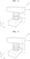
- FIG. 4 is a perspective view of a memory device 20 according to an embodiment.
- FIG. 5 is a perspective view of a memory device 20 according to another embodiment.
- the memory device 20 includes a first electrode layer 11, a switching material layer 12 arranged on the first electrode layer 11, a variable resistance layer 13 arranged on the switching material layer 12, and a second electrode layer 14 arranged on the variable resistance layer 13, and the switching material layer 12 includes a chalcogenide-based material as described above.
- the memory device 20 may further include a third electrode layer 15 between the switching material layer 12 and the variable resistance layer 13.
- the first electrode layer 11 and the second electrode layer 14 may be formed of the same conductive material materials as those of the first electrode layer 1 and the second electrode layer 3.
- the third electrode layer 15 may include a conductive material capable of generating sufficient heat in a phase change material of the variable resistance layer 13, which will be described later, without reacting with the memory device 20.
- the third electrode layer 15 may be formed of the same conductive material as those of the first electrode layer 1 and the second electrode layer 3, or may additionally include high-melting-point metals, or nitrides thereof such as TaSiN, TaAlN, WSi, TiW, MoN, NbN, TiBN, ZrSiN, WSiN, WBN, ZrAlN, MoAlN, TiAl, TiON, TiAlON, WON, TaON, antalum carbon nitride (TaCN), or combinations thereof.
- embodiments are not limited thereto.
- the variable resistance layer 13 may include a phase change material that reversibly changes between amorphous and crystalline states according to heating time.
- the phase change material may be in a high resistance state in an amorphous phase and a low resistance state in a crystalline phase.
- By defining the high resistance as '0' and the low resistance state as "1," data may be stored in the memory device 20.
- Examples of such a phase change material may include a chalcogenide-based material.
- the chalcogenide-based material may include a chalcogenide-based material having a different composition from the chalcogenide-based switching material.
- Examples of the chalcogenide-based material used in the variable resistance layer 13 may include a GeSbTe(GST)-based material.
- the GeSbTe(GST)-based material may be Ge 2 Sb 2 Te 5 , Ge 2 Sb 2 Te 7 , GeSb 2 Te 4 , or GeSb 4 Te 7 .
- the phase change material may include a chalcogenide material including two or more elements selected from silicon (Si), germanium (Ge), antimony (Sb), tellurium (Te), bismuth (Bi), indium (In), tin (Sn), and selenium (Se).
- the elements constituting the chalcogenide material may have various stoichiometric ratios.
- the memory device 20 includes a chalcogenide-based material as described above in the switching material layer 12, and thus, may have enhanced structural stability and a limited and/or suppressed threshold voltage drift.
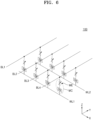
- FIG. 6 is an equivalent circuit diagram of a memory device 100 according to another embodiment.
- the memory device 100 may include wordlines WL1 and WL2 that extend in a first direction (X-direction) and are spaced from one another in a second direction (Y direction) perpendicular to the first direction.
- the memory device 100 may include bitlines BL1, BL2, BL3, and BL4 which are separated from the word lines WL 1 and WL2 in a third direction (Z direction) and extend in the second direction.
- Memory cells MC may be arranged between the bitlines BL1, BL2, BL3, and BL4 and the wordlines WL1 and WL2.
- the memory cells MC may be arranged at the crossing points of the bitlines BL1, BL2, BL3, and BL4 and the wordlines WL1 and WL2, and may include a variable resistance layer ME for information storage and a switching material layer SW for selecting a memory cell.
- the switching material layer SW may be also referred to as a selection element layer, a switching element layer, or an access element layer.
- Various voltage signals or current signals may be provided through the wordlines WL1 and WL2 and the bitlines BL1, BL2, BL3, and BL4, and data are written to or read from a memory cell selected according to a voltage signal or current signal, and the other unselected memory cells are prohibited from being written to or read from.
- the memory cells MC may be arranged in the same structure along the third direction.
- the switching material layer SW may be electrically connected to the wordline WL1
- the variable resistance layer ME may be electrically connected to the bitline BL1
- the variable resistance layer ME and the switching material layer SW may be connected in series.
- inventive concepts are not limited thereto.
- the positions of the switching material layer SW and the variable resistance layer ME in the memory cell MC may be switched.
- the variable resistance layer ME may be connected to the wordline WL1
- the switching material layer SW may be connected to the bitline BL1.
- variable resistance layers ME may be changed into one of a plurality of resistance states by an applied electric pulse.
- the variable resistance layers ME may include a phase change material of which a crystal state changes according to the amount of current.
- the phase change material may change into an amorphous state with a relatively high resistance or a crystal state with a relatively low resistance.
- the phase change material may undergo a phase change due to the Joule's heat generated according to the amount of current, and data may be written using the phase change.
- the phase change material may include a chalcogenide-based material.
- the variable resistance layers ME may have a multilayer structure in which two or more layers having different physical properties are stacked or a super-lattice structure in which a plurality of layers including different materials are alternately stacked.
- any memory cell MC may be addressed by selecting the wordline WL1 or WL2 and the bitline BL1, BL2, BL3, or BL4, and the memory cell MC may be programmed by applying a desired and/or alternatively predetermined signal between the selected wordline and the bitline.
- the memory cell MC may be programmed by measuring a current value through the bitlines BL1, BL2, BL3, and BL4, information according to a resistance value of the variable resistance layer ME of the corresponding memory cell MC, e.g., programmed information, may be read out.
- each memory cell MC may have a structure like one of the memory devices 20 described with reference to FIGS. 4 and 5 , where the first electrode layer 11 and second electrode layer 14 respectively may be portions of a corresponding word line (e.g., WL1) and a corresponding bit line (e.g., BL1). Alternatively, the first electrode layer 11 and second electrode layer 14 respectively may be portions of a corresponding word line (e.g., WL1) and a corresponding bit line (e.g., BL1). Alternatively, in some embodiments, each memory cell MC may have a structure like the memory cells MC1, MC3, and/or MC4 in the memory devices 200, 300, 400, and 500 described below with reference to FIGS. 7-8 , 9 , and 10 .
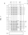
- FIG. 7 is a schematic planar layout diagram showing a partial configuration of a memory device 200 according to another embodiment.
- (A) is a cross-sectional view taken alone line X1 - X1' of FIG. 7
- (B) is a cross-sectional view taken alone line Y1 - Y1' of FIG. 7 .
- the memory device 200 includes a first electrode line layer arranged on a substrate 102 and including a plurality of first electrode lines 110 which extend in a first direction (X direction) and are spaced apart from each other; and a second electrode line layer arranged on the first electrode line layer and including a plurality of second electrode lines 170 which extend in a second direction (Y direction) different from the first direction (X-direction) and are spaced apart from each other.
- first direction (X direction) and the second direction (Y direction) are orthogonal to each other is described, but inventive concepts are not limited thereto.
- the plurality of first electrode lines 110 may be composed of the wordlines WL1 and WL2 as shown in FIG. 6
- the plurality of second electrode lines 170 may be composed of bitlines BL1, BL2, BL3, and BL4 as shown in FIG. 6
- the plurality of electrode lines 110 may be composed of the bitlines BL1, BL2, BL3, and BL4
- the plurality of second electrode lines 170 may be composed of the wordlines WL1 and WL2.
- the wordlines WL1 and WL2 may intersect the bitlines BL1, BL2, BL3, and BL4 to form crossing points, and at the crossing points, a plurality of memory cells MC1 electrically connected between the wordlines WL1 and WL2 and the bitlines BL1, BL2, BL3, and BL4 may be arranged.
- the plurality of memory cells MC1 may have a pillar structure in a rectangular pillar form as illustrated. However, embodiments are not limited thereto, and the memory cells may also have various pillar forms such as a cylindrical pillar, an elliptical pillar a polygonal pillar. In addition, the memory cells may have a structure with the lower portion wider than the upper portion or a structure with the upper portion wider than the lower portion, according to a method of forming the plurality of memory cells. For example, in the case where the plurality of memory cells are formed by an engraving etching process, the memory cells may have a structure with the lower portion wider than the upper portion.
- the memory cells may have a structure with the upper portion wider than the lower portion.
- the difference in width between the upper portion and the lower portion may be made to be almost zero by etching material layers such that the side is almost vertical, through precisely controlling the etching in the engraving etching process or damascene process.
- An interlayer insulating film 104 may be disposed on a substrate 102.
- the interlayer insulating film 104 may be an oxide film, a nitride film, or a combination thereof.
- the interlayer insulating film 104 may electrically isolate the plurality of first electrode lines 110 from the substrate 102.
- FIG. 8 illustrates a configuration with the interlayer insulating film 104 disposed on the substrate 102, inventive concepts are not limited thereto.
- an integrated circuit layer may be disposed on the substrate, and the plurality of memory cells MC1 may be disposed on the integrated circuit layer.
- the integrated circuit layer may include a peripheral circuit for operating the plurality of memory cells and/or a core circuit for arithmetic operations or the like.
- the plurality of first electrode lines 110 may be connected to drivers DRV.
- the drivers DRV may be circuits for applying a voltage to the plurality of first electrode lines 110.
- the drivers DRV may apply a voltage to respective access points of the plurality of first electrode lines 110 though interconnects.
- a selected memory cell MC1 may receive a voltage applied through a selected first electrode line 110 and a selected second electrode line 170.
- a voltage which corresponds to a difference in potential between the set high voltage and the set low voltage is applied to both ends of the selected memory cell MC1
- a set current flows through the selected memory cell MC1 and accordingly, current may flow through the plurality of first electrode lines 110 and the plurality of second electrode lines 170.
- a plurality of first insulation lines 112 are interposed between the plurality of first electrode lines 110, and a plurality of second insulation lines 172 are interposed between the plurality of second electrode lines 170.
- the plurality of first insulation lines 112 and the plurality of second insulation lines 172 may be silicon oxide films, silicon nitride films, or a combination thereof.
- the plurality of first electrode lines 110 and the plurality of second electrode lines 170 may be formed of the same conductive materials as those of the first electrode layer 11, the second electrode layer 14, or the third electrode layer 15.
- the plurality of first electrode lines 110 and the plurality of second electrode lines 170 may each further include a conductive barrier film.
- the conductive barrier film may include, for example, Ti, TiN, Ta, TaN, or a combination thereof.
- the plurality of first electrode lines 110 may be a metal film
- the plurality of second electrode lines 170 may be a multilayer including a conductive metal nitride film and a metal film.
- the plurality of memory cells MC1 arranged at the plurality of crossing points between the plurality of first electrode lines 110 and the plurality of second electrode line 170 may be insulated from each other by insulation structures 166.
- the insulation structures 166 may cover the sidewalls of the plurality of memory cells MC1, on the plurality of first insulation lines 112.
- the insulation structures 166 may include an encapsulation liner 162 which contacts the sidewall of each of the plurality of memory cells MC1, and a gap fill insulation film 164 which is spaced apart from each of the plurality of memory cells MC1 with the encapsulation liner 162 therebetween and fills, on the encapsulation liner 162, the space between the memory cells MC1.
- the plurality of first insulation lines 112, the plurality of second insulation lines 172, the encapsulation liners 162, and the gap fill insulation films 164 may each be silicon oxide films, silicon nitride films, or combinations thereof.
- the gap fill insulation films 164 may include a seam or an air gap.
- the term "air” may mean any gas present in atmosphere or during a manufacturing process.
- the first insulation lines 112 may be silicon nitride films
- the encapsulation liners 162 may be silicon oxide films, silicon nitride films, or a combination thereof
- the gap fill insulation films 164 may be silicon oxide films.
- the plurality of memory cells MC1 may each include a lower electrode BE, a switching material layer 124, a middle electrode ME, a lower barrier 132, a variable resistance layer 140, an upper barrier 134, and an upper electrode TE that are sequentially stacked on a first electrode line 110.
- the lower electrode BE, the middle electrode ME, the upper electrode TE may respectively include, for example: W, Ti, Ta, Al, Cu, C, CN, TiN, TiAlN, TiSiN, TiCN, TiCSiN, WN, CoSiN, WSiN, TaN, TaCN, TaSiN, or a combination thereof, but embodiments are not limited thereto.
- the switching material layer 124 may be configured to be electrically connected to the variable resistance layer 140.
- the switching material layer 124 may include a chalcogenide-based switching material and the chalcogenide-based switching material may include: a chalcogenide material including Ge, Sb, and Se; and a dopant, and the dopant may include at least one metal or metalloid element selected from In, Al, Sr, and Si, an oxide of the metal or metalloid element, or a nitride of the metal or metalloid element.
- the switching material layer 124 includes a chalcogenide-based switching material including any of the compounds represented by Formula 1.
- the switching material layer 124 includes a chalcogenide-based switching material having the composition according to the embodiments described above.
- the lower surface of the variable resistance layer 140 may contact the lower barrier 132, and the upper surface of the variable resistance layer 140 may contact the upper barrier 134.
- the lower barrier 132 and the upper barrier 134 may each include a conductive material, for example, W, WN, WC, or a combination thereof, but embodiments are not limited thereto.
- the switching material layer 124 may be connected to a first electrode line 110, which is one of the plurality of first electrode lines 110, by means of the lower electrode BE, and the variable resistance layer 140 may be connected to a second electrode line 170, which is one of the plurality of second electrode lines 170, by means of the upper barrier 134 and the upper electrode TE.
- the sidewalls of the lower electrode BE, the switching material layer 124, the middle electrode ME, the lower barrier 132, the variable resistance layer 140, the upper barrier 134, and the upper electrode TE are illustrated as extending in the vertical direction (Z direction), but inventive concepts are not limited thereto.
- the sidewalls of the lower electrode BE, the switching material layer 124, the middle electrode ME, the lower barrier 132, the variable resistance layer 140, the upper barrier 134, and the upper electrode TE may be tapered sidewalls.
- the switching material layer 124 includes a chalcogenide-based switching material as described above, and thus, structural stability may be enhanced even with aging.
- a threshold voltage drift may be suppressed.
- the plurality of memory cells MC1 may have a reduced threshold voltage drift, compared to a memory cell including a chalcogenide switching material consisting of Ge, Sb, and Se.
- FIG. 9 shows cross-sectional views of a memory device according to another embodiment.
- the same reference numerals as in FIG. 8 indicate the same members, and redundant descriptions thereof are omitted here.
- (A) and (B) show partial configurations of portions corresponding to cross-sections taken along line X1 - X1' and line Y1 - Y1' of FIG. 7 , respectively.
- a memory device 300 may have mostly the same configuration as that of the memory device 200 described with reference to FIG. 7 , and (A) and (B) of FIG. 8 .
- the memory device 300 includes a plurality of memory cells MC3, instead of the plurality of memory cells MC1.
- the plurality of memory cells MC3 may have almost the same configuration as the plurality of memory cells MC1 described with reference to FIG. 7 , and (A) and (B) of FIG. 8 .
- the plurality of memory cells MC3 may each include a lower electrode BE, a lower barrier 132, a variable resistance layer 140, an upper barrier 134, a middle electrode ME, a switching material layer 124, and an upper electrode TE, which are sequentially stacked on a first electrode line 110.
- variable resistance layer 140 may be connected to a first electrode line 110, which is one of the plurality of first electrode lines 110, by means of the lower barrier 132 and the lower electrode BE, and the switching material layer 124 may be connected to a second electrode line 170, which is one of the plurality of second electrode lines 170, by means of the upper electrode TE.
- FIG. 10 shows cross-sectional views of a memory device according to another embodiment.
- the same reference numerals as in FIG. 7 and (A) and (B) of FIG. 8 indicate the same members, and redundant descriptions thereof are omitted here.
- (A) and (B) show partial configurations of portions of cross-sections taken along line X1 - X1' and line Y1 - Y1' of FIG. 7 , respectively.
- a memory device 500 may include: a first electrode line layer including a plurality of first electrode lines 110 which extend in a first direction (X direction) on a substrate 102 and are arranged spaced apart from each other; a second electrode line layer including a plurality of second electrode lines 170 which are arranged on the first electrode line layer, extend in a second direction (Y direction) different from the first direction, and are spaced apart from each other; and a plurality of third electrode lines 510 which are arranged on the second electrode line layer, extend in the first direction (X direction), and are spaced apart from each other.
- a plurality of third insulation lines 512 may be interposed between the plurality of third electrode lines 510.
- the plurality of third insulation lines 512 may include silicon oxide films, silicon nitride films, or a combination thereof.
- a plurality of first level memory cells MC51 may be arranged respectively at a plurality of crossing points between the plurality of first electrode lines 110 and the plurality of second electrode lines 170, and a plurality of second level memory cells MC52 may be arranged respectively at a plurality of crossing points between the plurality of second electrode lines 170 and the plurality of third electrode lines 510.
- the plurality of first level memory cells MC51 and the plurality of second level memory cells MC52 may be formed at different levels in a vertical direction (Z direction).
- the plurality of first level memory cells MC51 and the plurality of second level memory cells MC52 may have mostly the same configuration as that of the plurality of memory cells MC1 described with reference to FIG. 8 .
- the upper electrode TE of each of the plurality of second level memory cells MC52 may be connected to one third electrode line 510 selected from the plurality of third electrode lines 510.
- the plurality of first electrode lines 110, the plurality of second electrode lines 170, and the plurality of third electrode lines 510 may each include a plurality of wordlines or a plurality of bitlines.
- the plurality of first electrode lines 110 and the plurality of third electrode lines 510 may each constitute a plurality of bitlines, and the plurality of second electrode lines 170 may constitute a common wordline.
- the plurality of first electrode lines 110 and the plurality of third electrode lines 510 may each constitute a plurality of wordlines, and the plurality of second electrode lines 170 may constitute a common bitline.
- the constituent material of the plurality of third electrode lines 510 may be mostly the same as described above with respect to the plurality of first electrode lines 110 and the plurality of second electrode lines 170 illustrated in FIG. 8 .
- the memory device 500 may have a two-layer stack structure including the plurality of first level memory cells MC51 and the plurality of second level memory cells MC52, which are formed at two different levels in the vertical direction (Z direction).
- FIG. 10 illustrates the embodiment in which the plurality of first level memory cells MC51 and the plurality of second level memory cells MC52 have mostly the same configuration as that of the plurality of memory cells MC1 described with reference to FIG. 8 , inventive concepts are not limited thereto.
- the plurality of first level memory cells MC51 and the plurality of second level memory cells MC52 may include a switching material layer 124 including a chalcogenide-based switching material as described above.
- Cohesive energy refers to the energy required for a structure formed by the first principle (Ab initio) calculation method to stabilize with time. It was determined that a structure with low cohesive energy had considerable structural relaxation, and thus threshold voltage drift using cohesive energy and bandgap energy was evaluated.
- a switching element was obtained with each element having a cross-point structure composed of metal (lower electrode, Pt 50 nm)/switching material layer (30 nm)/metal (upper electrode, TiN 50 nm) using photolithography and lift-off techniques.
- switching material layers chalcogenide-based material (Ge 20 Sb 20 Se 60 In 5 ) thin films were used as switching material layers.
- the Ge 20 Sb 20 Se 60 In 5 thin films were each formed by co-sputtering deposition using Ge, Sb, Se, and In targets.
- the compositions of the thin films were adjusted by changing radio-frequency (RF) power imposed on each target.
- RF radio-frequency
- composition contents of Ge, Sb, Se, and In were determined to be 20 at%, 20 at%, 60 at%, and 5 at%, respectively, by Electron Prob Micro Analysis (EPMA) and X-ray Fluorescence (XRF) analysis.
- EPMA Electron Prob Micro Analysis
- XRF X-ray Fluorescence
- the size of a cross-point structure element was defined with the overlapping area of the upper and lower electrode metals. According to FIG. 6 , a memory device including the switching element was obtained.
- a memory device was obtained in the same manner as in Example 1, except that a chalcogenide-based material (Ge 20 Sb 20 Se 60 In 10 ) thin films were used as switching material layers and that the composition contents of Ge, Sb, Se, and In were determined to be 20 at%, 20 at%, 60 at%, and 10 at%, respectively, by EPMA and XRF analysis.
- a chalcogenide-based material Ge 20 Sb 20 Se 60 In 10
- a memory device was obtained in the same manner as in Example 1, except that a chalcogenide-based material (Ge 20 Sb 20 Se 60 ) thin films were used as switching material layers and that the composition contents of Ge, Sb, and Se were determined to be 20 at%, 20 at%, 60 at%, respectively, by EPMA and XRF analysis.
- a chalcogenide-based material Ge 20 Sb 20 Se 60
- the composition contents of Ge, Sb, and Se were determined to be 20 at%, 20 at%, 60 at%, respectively, by EPMA and XRF analysis.
- Table 1 shows the results of evaluation of threshold voltage drift (Vth_drift) for memory devices including switching material layers having compositions according to Examples 1 and 2 and Comparative Example 1. Threshold voltage drifts and threshold voltage drift reduction rates of the memory devices were evaluated by the following method.
- Threshold voltage drift reduction rate (%) [ ⁇ (Vth_drift of Comparative Example 1) - (Vth_drift of Example 1 (or 2))/(Vth_drift of Comparative Example 1) ⁇ ⁇ 100] [Table 1] Vth_drift (mV/dec) Vth_drift reduction rate (%) Comparative Example 1 49.5 - Example 1 36.3 26 Example 2 9.1 81
- the threshold drifts of the memory devices including the chalcogenide-based materials of Example 1 (Ge 20 Sb 20 Se 60 In 5 ) and Example 2 (Ge 20 Sb 20 Se 60 In 10 ) as the switching material layers were lower compared to the memory device including the chalcogenide-based material of Comparative Example 1 (Ge 20 Sb 20 Se 60 ).
- the memory devices including the chalcogenide-based materials of Example 1 (Ge 20 Sb 20 Se 60 In 5 ) and Example 2 (Ge 20 Sb 20 Se 60 In 10 ) had a threshold voltage drift reduction rate of 25% and 81%, respectively, compared to that of the memory device including the chalcogenide-based material of Comparative Example 1 (Ge 20 Sb 20 Se 60 ).
- the chalcogenide-based material includes: a chalcogenide material including Ge, Sb, and Se; and a dopant, wherein the dopant includes at least one metal or metalloid element selected from In, Al, Sr, and Si, an oxide of the metal or metalloid element, or a nitride of the metal or metalloid element.
- a switching element and a memory device which use the chalcogenide-based material in a switching material layer may have enhanced structural stability and suppressed threshold voltage drift.
- the memory devices according to the embodiments of inventive concepts in the present disclosure may have enhanced structural stability and limited and/or suppressed threshold voltage drift.
- FIG. 11 is a diagram of an electronic device including a memory device according to example embodiments.
- an electronic device 1000 may include a controller 700, a memory controller 550, a display device 600 (e.g., OLED display, holographic display), and a memory device 100.
- the memory controller 550 may include a read/write circuit 560 and a word line driver circuit 570.
- the read/write circuit 560 and word line driver circuit 570 may be electrically connected to the memory device 100 through first electrode lines (e.g., WL1) and second electrode lines (e.g., BL1).
- the controller 700 may control operations of the electronic device 1000 and may include processing circuitry 710, a host interface 715, and a power management circuit 720.
- the memory device 100 may be implemented using any one of the memory devices 20, 100, 200, 300, and 500 described above with reference to FIGS. 4-10 .
- the processing circuitry 710 may operate in response to those commands and may control operations of the display device 600, memory controller 550, and/or memory device 100.
- the controller 700 may control the display device 600 by providing commands and information to the display device 600 and by controlling power to the display device 600 using the power management circuit 720.
- the controller 700 may control power provided to the memory controller 550 and memory device 100 using the power management circuit 720.
- the controller 700 may control operations of the memory device 100 by providing commands to the memory controller 550.
- the controller 700 may also provide the memory controller 550 with data to be written in the memory device 100 and/or may receive data read from the memory device 100.
- the memory controller 550 in response to receiving commands from the controller 700 and/or in response to receiving data for a write operation, may control the memory device 100 using the read/write circuit 560 and word line driver circuit 570 to write data, read data, and/or erase data in one or more selected semiconductor unit devices MC of the memory device 100.
- the memory controller 550 in response to receiving commands from the controller 700, may read data from the memory device 100 and provide the data read from the memory device 100 to the controller 700.
- processing circuitry such as hardware including logic circuits; a hardware/software combination such as a processor executing software; or a combination thereof.
- the processing circuitry more specifically may include, but is not limited to, a central processing unit (CPU), an arithmetic logic unit (ALU), a digital signal processor, a microcomputer, a field programmable gate array (FPGA), a System-on-Chip (SoC), a programmable logic unit, a microprocessor, application-specific integrated circuit (ASIC), etc.
- CPU central processing unit
- ALU arithmetic logic unit
- FPGA field programmable gate array
- SoC System-on-Chip
- ASIC application-specific integrated circuit
Landscapes
- Chemical & Material Sciences (AREA)
- Organic Chemistry (AREA)
- Chemical Kinetics & Catalysis (AREA)
- Engineering & Computer Science (AREA)
- Materials Engineering (AREA)
- Mechanical Engineering (AREA)
- Metallurgy (AREA)
- Crystallography & Structural Chemistry (AREA)
- Inorganic Chemistry (AREA)
- Semiconductor Memories (AREA)
Description
- The present disclosure relates to a chalcogenide-based material, and a switching device and/or a memory device that include the same.
- With the development of compact and high-performance electronic devices in recent years, there is a demand for memory devices capable of storing information in various electronic devices such as computers and portable communication devices. Such memory devices may include resistive random-access memory (RRAM), phase-change random access memory (PRAM), and magnetic random-access memory (MRAM), in which data is stored using properties of switching between different resistance states in accordance with voltage or current applied thereto. Such a memory device may require a switching material layer that allows selective addressing to a material layer capable of storing data. For the switching material layer, a chalcogenide switching material including Ge, As, and Se has been used. However, the use of As may cause a problem of environmental pollution due to its risk of toxicity.
- There may be a need for a chalcogenide-based material of a novel composition, and a switching device and a memory device that include the chalcogenide-based material.
-
US2020/0365801A1 discloses a switching element includes a lower barrier electrode on a substrate, a switching pattern on the lower barrier electrode, and an upper barrier electrode on the switching pattern. -
KR20210027306A -
KR20200132366A -
EP3660932A1 discloses a composition comprising selenium, arsenic, at least one of boron, aluminum, gallium, indium, or thallium, and optionally germanium or silicon. - Sharda et Al, Journal of ELECTRONIC MATERIALS, Vol. 42, No. 12, 2013, pages 3367-3372 discloses "New Quaternary Sb-Se-Ge-In Chalcogenide Glasses: Linear and Nonlinear Optical Properties".
- Sharda et Al, Journal of Alloys and Compounds 611 (2014) 96-99 discloses "Thermal stability and crystallization kinetics of quaternary Sb-Se-Ge-In chalcogenide glasses".
- In a first aspect, there is provided a switching element as defined in
claim 1. One or more embodiments include a chalcogenide-based material having an As-free novel composition. - One or more embodiments include a switching device that uses the chalcogenide-based material in a switching material layer to have enhanced structural stability and/or suppressed threshold voltage drift.
- In a second aspect, there is provided a memory device as defined in claim 4. In a third aspect, there is provided a memory device as defined in claim 7. One or more embodiments include a memory device that uses the chalcogenide-based material in a switching material layer to have enhanced structural stability and suppressed threshold voltage drift.
- Additional aspects will be set forth in part in the description which follows and, in part, will be apparent from the description, or may be learned by practice of the presented embodiments of the disclosure.
- The above and other aspects, features, and advantages of certain embodiments of the disclosure will be more apparent from the following description taken in conjunction with the accompanying drawings, in which:
-
FIG. 1 is a three-dimensional compositional diagram showing composition regions of a chalcogenide-based material according to an embodiment; -
FIG. 2 is a schematic view of a switching element according to an embodiment; -
FIGS. 3A and 3B show the results of extended x-ray absorption fine structure (EXAFS) analysis of the bonding structures of elements in Ge20Sb20Se60In5 and Ge20Sb20Se60In10 chalcogenide-based switching materials of switching elements ; -
FIG. 4 is a perspective view of a memory device according to an embodiment; -
FIG. 5 is a perspective view of a memory device according to another embodiment; -
FIG. 6 is an equivalent circuit diagram of a memory device according to another embodiment; -
FIG. 7 is a schematic planar layout diagram showing a partial configuration of a memory device according to another embodiment; -
FIG. 8 shows cross-sectional views (A) and (B) taken along line X1 - X1' and line Y1 - Y1' ofFIG. 7 , respectively; -
FIG. 9 shows cross-sectional views of a memory device according to another embodiment; -
FIG. 10 shows cross-sectional views of a memory device according to another embodiment; and -
FIG. 11 is a diagram of an electronic device including a memory device according to example embodiments. - Reference will now be made in detail to embodiments, examples of which are illustrated in the accompanying drawings, wherein like reference numerals refer to like elements throughout. In this regard, the present embodiments may have different forms and should not be construed as being limited to the descriptions set forth herein. Accordingly, the embodiments are merely described below, by referring to the figures, to explain aspects. As used herein, the term "and/or" includes any and all combinations of one or more of the associated listed items. Expressions such as "at least one of," when preceding a list of elements, modify the entire list of elements and do not modify the individual elements of the list. For example, "at least one of A, B, and C," and similar language (e.g., "at least one selected from the group consisting of A, B, and C") may be construed as A only, B only, C only, or any combination of two or more of A, B, and C, such as, for instance, ABC, AB, BC, and AC.
- Hereinafter, embodiments of a chalcogenide-based material, and a switching element and a memory device which include the same will be described in detail. Accordingly, it should be apparent to those skilled in the art that the following description of various embodiments of the present disclosure is provided for illustration purpose only and not for the purpose of limiting the present disclosure as defined by the appended claims and their equivalents.
- Hereinafter, an element referred to as being "above" or "on" another element may be directly on the other element in contact therewith or intervening elements may also be present. As used herein, the singular forms "a", "an" and "the" are intended to include the plural forms as well, unless the context clearly indicates otherwise. Throughout the specification, the term "include" is intended to indicate that an element do not preclude the other elements but further add and/or intervene another element, unless otherwise stated. As used herein, the term "combination" includes a mixture, an alloy, a reaction product, and the like unless otherwise stated. It will be understood that, although the terms first, second, third, fourth, etc. may be used herein to describe various components, these components should not be limited by these terms. These terms are only used to distinguish one component from another. The term "or" refers to "and/or" unless otherwise stated.
- As used herein, the term "connected" may refer to being connected directly or indirectly, or via a communication network. As used herein, the terms "an embodiment", "embodiments", and the like indicate that elements described with regard to an embodiment are included in at least one embodiment described in this specification and may or may not present in other embodiments. In addition, it may be understood that the described elements are combined in any suitable manner in various embodiments. Unless otherwise defined, technical and scientific terms used herein have the same meaning as commonly understood by one or ordinary skill in the art to which this application belongs.
- However, in the event of any conflict or inconsistency between terms used herein and terms of the cited references, the terms used in this specification take precedence over the terms of the cited references. While particular embodiments have been described, alternatives, modifications, variations, improvements, and substantial equivalents that are or may be presently unforeseen may arise to applicants or others skilled in the art. Accordingly, the appended claims are intended to embrace all such alternatives, modification, variations, improvements, and substantial equivalents.
- When the terms "about" or "substantially" are used in this specification in connection with a numerical value, it is intended that the associated numerical value includes a manufacturing or operational tolerance (e.g., ±10%) around the stated numerical value. Moreover, when the words "generally" and "substantially" are used in connection with geometric shapes, it is intended that precision of the geometric shape is not required but that latitude for the shape is within the scope of the disclosure. Further, regardless of whether numerical values or shapes are modified as "about" or "substantially," it will be understood that these values and shapes should be construed as including a manufacturing or operational tolerance (e.g., ±10%) around the stated numerical values or shapes.
- In general, an ovonic threshold switching (OTS) material includes arsenic (As). For example, an OTS material may include Ge-As-Te-Si, Ge-As-Se, Ge-As-Te, or the like. Arsenic helps to maintain the amorphous state of an OTS material, and thus limits and/or prevents a phenomenon of irreversible switching due to a phase change. However, since As materials are toxic and have many restrictions on their use, research is ongoing for replacement with other materials.
- Research has been conducted on Ge-Sb-Te, Ge-P-Se, Ge-Te, Ge-Se, and the like as As-free chalcogenide-based switching materials. Of these materials, the Ge-Sb-Te material is excellent in amorphous stability and electrical characteristics, but has lower structural stability compared to As-containing chalcogenide-based switching materials. This results from that Sb atom has a larger size than As atom and thus easily forms a crystalline phase. Due to such a low structural stability, Ge-Sb-Se-based switching elements and memory devices have a relatively large threshold voltage drift caused by structural relaxation.
- Considering such problems, the inventors of the present disclosure proposes, as below, a chalcogenide-based material having a novel composition, and a switching element and a memory device that include the same.
-
FIG. 1 is a three-dimensional compositional diagram showing composition regions of a chalcogenide-based material according to an embodiment. - Referring to
FIG. 1 , the chalcogenide-based material according to an embodiment has a composition including about 10 at% to about 40 at% of Ge element, about 10 at% to about 50 at% of Sb element, about 30 at% to about 80 at% of Se element, and about 0.5 at% to about 10 at% of a dopant element. - The chalcogenide-based material includes a compound represented by Formula 1:
[Formula 1] GeaSbbSecMd
wherein, inFormula 1, - M may be at least one metal or metalloid element selected from In, Al, Sr, and Si,
- 10 at% ≤ a ≤ 40 at%, 10 at% ≤ b ≤ 50 at%, 30 at% ≤ c ≤ 80 at%, 0.5 at% ≤ d ≤ 10 at%, and
-

- For example, in
Formula - For example, in
Formula - When the chalcogenide-based material is used in a switching element, there may be a reduction in Se-Se homopolar bonds that play an important role in structural relaxation occurring with aging. Instead, bonds between Se-dopant metal or metalloid atoms may increase. This may cause the chalcogenide-based material to have enhanced structural stability and may limit and/or suppress a threshold voltage drift.
-
FIG. 2 is a schematic view of a switchingelement 10 according to an embodiment. - Referring to
FIG. 2 , the switchingelement 10 includes afirst electrode layer 1, asecond electrode layer 3 arranged to face thefirst electrode layer 1, and a switchingmaterial layer 2 between thefirst electrode layer 1 and thesecond electrode layer 3, wherein the switchingmaterial layer 2 includes the chalcogenide-based material as described above. - The
first electrode layer 1 and thesecond electrode layer 3 serve as a path of a current. Thefirst electrode layer 1 and thesecond electrode layer 3 may be formed at both ends of switchingmaterial layer 2, respectively. In other embodiments, thefirst electrode layer 1 and thesecond electrode layer 3 may optionally be formed of conductive materials. For example, the conductive materials may each be a metal, a conductive metal nitride, a conductive metal oxide, or a combination thereof. For example, the conductive materials may each include at least one selected from carbon (C), a titanium nitride (TiN), a titanium silicon nitride (TiSiN), a titanium carbon nitride (TiCN), a titanium carbon silicon nitride (TiCSiN), a titanium aluminum nitride (TiAIN), tantalum (Ta), a tantalum nitride (TaN), tungsten (W), and a tungsten nitride (WN), but are not limited thereto. - The switching
material layer 2 may be a current control layer capable of controlling flow of a current. - The switching
material layer 2 includes a chalcogenide-based switching material according to any of the embodiments described above. - The switching
material layer 2 may be formed by deposition, for example, by physicochemical deposition. - In one or more embodiments, the switching
material layer 2 may be formed by physical vapor deposition using at least one target which includes: a chalcogenide material including Ge, Sb, and Se; and a dopant which is at least one metal or metalloid element selected from In, Al, Sr, and Si. In an embodiment, the at least one target may include a first target that includes: both a chalcogenide material including Ge, Sb, and Se; and a dopant including at least one metal or metalloid element selected from In, Al, Sr, and Si. In other embodiments, the at least one target may include: a first target including Ge, Sb, and Se elements; and a second target including a dopant including at least one metal or metalloid element selected from In, Al, Sr, and Si. - In other embodiments, the switching material layer may be formed by chemical vapor deposition (CVD) or atomic layer deposition (ALD) using a plurality of sources that include: a chalcogenide material including Ge, Sb, and Se; and a dopant including at least one metal or metalloid element selected from In, Al, Sr, and Si, an oxide of the metal or metalloid element, or a nitride of the metal or metalloid element.
- In other embodiments, the switching
material layer 2 may be formed to have a small thickness by co-sputtering deposition. A thickness of the switchingmaterial layer 2 may be about 5 nm to about 50 nm, for example, about 5 nm to about 30 nm. - The chalcogenide-based switching material of the switching
material layer 2 may exhibit an ovonic threshold switching (OTS) material characteristic. - When a voltage less than a threshold voltage is applied across the
first electrode layer 1 and thesecond electrode layer 3, the switchingmaterial layer 2 maintains a high resistance state with little current flowing, and when a voltage higher than the threshold voltage is applied across thefirst electrode layer 1 and thesecond electrode layer 3, the switchingmaterial layer 2 becomes a low resistance state and a current may begin to flow therethrough. In addition, when the current flowing through the switchingmaterial layer 2 falls to below a holding current, the switchingmaterial layer 2 may change into a high resistance state. - The structural stability of the chalcogenide-based switching material of the switching
material layer 2 may be enhanced, and thus, the switchingelement 10 may implement stable switching characteristics with a limited and/or suppressed threshold voltage drift. This results from bonding of the dopant with at least portion of Se atom in the chalcogenide-based switching material. The chalcogenide-based switching material may be an amorphous material in which at least some Se-Se homopolar bonds are substituted with Se-M bonds, wherein M may be a metal or metalloid element of In, Al, Sr, or Si. -
FIGS. 3A and 3B show the results of extended x-ray absorption fine structure (EXAFS) analysis of the bonding structures of elements in Ge20Sb20Se60In5 and Ge20Sb20Se60In10 chalcogenide-based switching materials of switching elements. InFIGS. 3A and 3B , the bar on the left represents the numbers of Se atoms, Sb atoms, and Ge atoms that bind with one Ge atom. InFIGS. 3A and 3B , the bar in the middle represents the numbers of Se atoms, Sb atoms, and Ge atoms that bind with one Sb atom. InFIGS. 3A and 3B , the bar on the right represents the numbers of Se atoms, Sb atoms, Ge atoms, and dopant atoms bound to one Se atom. - Referring to
FIG. 3A , for the Ge20Sb20Se60In5 chalcogenide-based switching material, the number of Se atoms that bind with one Ge atom was 2.9, the number of Sb atoms that bind with one Ge atom was 0.2, the number of Ge atoms that bind with one Ge atom was 0.3. For the Ge20Sb20Se60In5 chalcogenide-based switching material, the number of Se atoms that bind with one Sb atom was 2.5, the number of Sb atoms that bind with one Sb atom was 0.05, and the number of Ge atoms that bind with one Sb atom was 0.2. For the Ge20Sb20Se60In5 chalcogenide-based switching material, the number of Se atoms that bind with one Se atom was 0.23, the number of Sb atoms that bind with one Se atom was 0.84, the number of Ge atoms that bind with one Se atom was 0.95, and the number of In atoms that bind with one Se atom was 0.35. - Referring to
FIG. 3B , for the Ge20Sb20Se60In10 chalcogenide-based switching material, the number of Se atoms that bind with one Ge atom was 2.85, the number of Sb atoms that bind with one Ge atom was 0.18, and the number of Ge atoms that bind to one Ge atom was 0.28. For the Ge20Sb20Se60In10 chalcogenide-based switching material, the number of Se atoms that bind with one Sb atom was 2.31, the number of Sb atoms that bind with one Sb atom was 0.04, and the number of Ge atoms that bind with one Sb atom was 0.17. For the Ge20Sb20Se60In10 chalcogenide-based switching material, the number of Se atoms that bind with one Se atom was 0.16, the number of Sb atoms that bind with one Se atom was 0.78, the number of Ge atoms that bind with one Se atom was 0.9, and the number of In atoms that bind with one Se atom was 0.48. - From
FIGS. 3A and 3B , for the Ge20Sb20Se60In5 and Ge20Sb20Se60In10 chalcogenide-based switching materials of the switching elements, it can be confirmed that In atoms were bound to Se atoms, and as the amount of In atoms increased from 5 at% to 10 at%, the number of bonds between Se atoms reduced, and the number of bonds between Se atoms and In atoms increased. These analysis results are considered to be due to a higher binding energy of Se-M bonds compared to Se-Se homopolar bonds. According to Practical Electron Microscopy and Database (Yougui Liao, Second Edition, 2006), the binding energy of Se-Se homopolar bonds is 172 kJ/mol. In comparison to this, the Se-In binding energy is 245 kJ/mol, the Se-Al binding energy is 318 kJ/mol, the Se-Sr binding energy is 251 kJ/mol, and the Se-Si binding energy is 538 kJ/mol. Accordingly, the chalcogenide-based switching materials may have enhanced structural stability even with aging. The switchingelement 10 may have a reduced threshold voltage drift, compared to the chalcogenide switching material consisting of Ge, Sb, and Se. -
FIG. 4 is a perspective view of amemory device 20 according to an embodiment.FIG. 5 is a perspective view of amemory device 20 according to another embodiment. - Referring to
FIG. 4 , thememory device 20 includes afirst electrode layer 11, a switchingmaterial layer 12 arranged on thefirst electrode layer 11, avariable resistance layer 13 arranged on the switchingmaterial layer 12, and asecond electrode layer 14 arranged on thevariable resistance layer 13, and the switchingmaterial layer 12 includes a chalcogenide-based material as described above. Referring toFIG. 5 , thememory device 20 may further include athird electrode layer 15 between the switchingmaterial layer 12 and thevariable resistance layer 13. Thefirst electrode layer 11 and thesecond electrode layer 14 may be formed of the same conductive material materials as those of thefirst electrode layer 1 and thesecond electrode layer 3. Thethird electrode layer 15 may include a conductive material capable of generating sufficient heat in a phase change material of thevariable resistance layer 13, which will be described later, without reacting with thememory device 20. Thethird electrode layer 15 may be formed of the same conductive material as those of thefirst electrode layer 1 and thesecond electrode layer 3, or may additionally include high-melting-point metals, or nitrides thereof such as TaSiN, TaAlN, WSi, TiW, MoN, NbN, TiBN, ZrSiN, WSiN, WBN, ZrAlN, MoAlN, TiAl, TiON, TiAlON, WON, TaON, antalum carbon nitride (TaCN), or combinations thereof. However, embodiments are not limited thereto. - The
variable resistance layer 13 may include a phase change material that reversibly changes between amorphous and crystalline states according to heating time. The phase change material may be in a high resistance state in an amorphous phase and a low resistance state in a crystalline phase. By defining the high resistance as '0' and the low resistance state as "1," data may be stored in thememory device 20. Examples of such a phase change material may include a chalcogenide-based material. The chalcogenide-based material may include a chalcogenide-based material having a different composition from the chalcogenide-based switching material. Examples of the chalcogenide-based material used in thevariable resistance layer 13 may include a GeSbTe(GST)-based material. For example, the GeSbTe(GST)-based material may be Ge2Sb2Te5, Ge2Sb2Te7, GeSb2Te4, or GeSb4Te7. However, embodiments are not limited thereto, and the phase change material may include a chalcogenide material including two or more elements selected from silicon (Si), germanium (Ge), antimony (Sb), tellurium (Te), bismuth (Bi), indium (In), tin (Sn), and selenium (Se). The elements constituting the chalcogenide material may have various stoichiometric ratios. - The
memory device 20 includes a chalcogenide-based material as described above in the switchingmaterial layer 12, and thus, may have enhanced structural stability and a limited and/or suppressed threshold voltage drift. -
FIG. 6 is an equivalent circuit diagram of amemory device 100 according to another embodiment. - Referring to
FIG. 6 , thememory device 100 may include wordlines WL1 and WL2 that extend in a first direction (X-direction) and are spaced from one another in a second direction (Y direction) perpendicular to the first direction. In addition, thememory device 100 may include bitlines BL1, BL2, BL3, and BL4 which are separated from the word linesWL 1 and WL2 in a third direction (Z direction) and extend in the second direction. - Memory cells MC may be arranged between the bitlines BL1, BL2, BL3, and BL4 and the wordlines WL1 and WL2. In particular, the memory cells MC may be arranged at the crossing points of the bitlines BL1, BL2, BL3, and BL4 and the wordlines WL1 and WL2, and may include a variable resistance layer ME for information storage and a switching material layer SW for selecting a memory cell. The switching material layer SW may be also referred to as a selection element layer, a switching element layer, or an access element layer. Various voltage signals or current signals may be provided through the wordlines WL1 and WL2 and the bitlines BL1, BL2, BL3, and BL4, and data are written to or read from a memory cell selected according to a voltage signal or current signal, and the other unselected memory cells are prohibited from being written to or read from.
- The memory cells MC may be arranged in the same structure along the third direction. For example, in the memory cell MC arranged between a wordline WL1 and a bitline BL1, the switching material layer SW may be electrically connected to the wordline WL1, the variable resistance layer ME may be electrically connected to the bitline BL1, and the variable resistance layer ME and the switching material layer SW may be connected in series. However, inventive concepts are not limited thereto. For example, unlike the illustration in
FIG. 6 , the positions of the switching material layer SW and the variable resistance layer ME in the memory cell MC may be switched. For example, in the memory cell MC, the variable resistance layer ME may be connected to the wordline WL1, and the switching material layer SW may be connected to the bitline BL1. - A method of driving the
memory device 100 will be briefly described as below. In thememory device 100, a voltage may be applied to the memory cells MC through the wordlines WL1 and WL2 and the bitlines BL1, BL2, BL3, and BL4, so that a current flows in the variable resistance layers ME. The variable resistance layers ME may be changed into one of a plurality of resistance states by an applied electric pulse. The variable resistance layers ME may include a phase change material of which a crystal state changes according to the amount of current. The phase change material may change into an amorphous state with a relatively high resistance or a crystal state with a relatively low resistance. The phase change material may undergo a phase change due to the Joule's heat generated according to the amount of current, and data may be written using the phase change. The phase change material may include a chalcogenide-based material. If necessary, the variable resistance layers ME may have a multilayer structure in which two or more layers having different physical properties are stacked or a super-lattice structure in which a plurality of layers including different materials are alternately stacked. - In addition, any memory cell MC may be addressed by selecting the wordline WL1 or WL2 and the bitline BL1, BL2, BL3, or BL4, and the memory cell MC may be programmed by applying a desired and/or alternatively predetermined signal between the selected wordline and the bitline. In addition, by measuring a current value through the bitlines BL1, BL2, BL3, and BL4, information according to a resistance value of the variable resistance layer ME of the corresponding memory cell MC, e.g., programmed information, may be read out.
- In some embodiments, each memory cell MC may have a structure like one of the
memory devices 20 described with reference toFIGS. 4 and 5 , where thefirst electrode layer 11 andsecond electrode layer 14 respectively may be portions of a corresponding word line (e.g., WL1) and a corresponding bit line (e.g., BL1). Alternatively, thefirst electrode layer 11 andsecond electrode layer 14 respectively may be portions of a corresponding word line (e.g., WL1) and a corresponding bit line (e.g., BL1). Alternatively, in some embodiments, each memory cell MC may have a structure like the memory cells MC1, MC3, and/or MC4 in thememory devices FIGS. 7-8 ,9 , and10 . -
FIG. 7 is a schematic planar layout diagram showing a partial configuration of amemory device 200 according to another embodiment. InFIG. 8 , (A) is a cross-sectional view taken alone line X1 - X1' ofFIG. 7 , and (B) is a cross-sectional view taken alone line Y1 - Y1' ofFIG. 7 . - As illustrated in
FIGS. 7 and (A) ofFIG. 8 , thememory device 200 according to an embodiment includes a first electrode line layer arranged on asubstrate 102 and including a plurality offirst electrode lines 110 which extend in a first direction (X direction) and are spaced apart from each other; and a second electrode line layer arranged on the first electrode line layer and including a plurality ofsecond electrode lines 170 which extend in a second direction (Y direction) different from the first direction (X-direction) and are spaced apart from each other. In the present embodiment, a case where the first direction (X direction) and the second direction (Y direction) are orthogonal to each other is described, but inventive concepts are not limited thereto. In an embodiment, the plurality offirst electrode lines 110 may be composed of the wordlines WL1 and WL2 as shown inFIG. 6 , and the plurality ofsecond electrode lines 170 may be composed of bitlines BL1, BL2, BL3, and BL4 as shown inFIG. 6 . In another embodiment, the plurality ofelectrode lines 110 may be composed of the bitlines BL1, BL2, BL3, and BL4, and the plurality ofsecond electrode lines 170 may be composed of the wordlines WL1 and WL2. The wordlines WL1 and WL2 may intersect the bitlines BL1, BL2, BL3, and BL4 to form crossing points, and at the crossing points, a plurality of memory cells MC1 electrically connected between the wordlines WL1 and WL2 and the bitlines BL1, BL2, BL3, and BL4 may be arranged. - The plurality of memory cells MC1 may have a pillar structure in a rectangular pillar form as illustrated. However, embodiments are not limited thereto, and the memory cells may also have various pillar forms such as a cylindrical pillar, an elliptical pillar a polygonal pillar. In addition, the memory cells may have a structure with the lower portion wider than the upper portion or a structure with the upper portion wider than the lower portion, according to a method of forming the plurality of memory cells. For example, in the case where the plurality of memory cells are formed by an engraving etching process, the memory cells may have a structure with the lower portion wider than the upper portion. In addition, in the case where the plurality of memory cells are formed by a damascene process, the memory cells may have a structure with the upper portion wider than the lower portion. However, the difference in width between the upper portion and the lower portion may be made to be almost zero by etching material layers such that the side is almost vertical, through precisely controlling the etching in the engraving etching process or damascene process.
- An interlayer insulating
film 104 may be disposed on asubstrate 102. Theinterlayer insulating film 104 may be an oxide film, a nitride film, or a combination thereof. Theinterlayer insulating film 104 may electrically isolate the plurality offirst electrode lines 110 from thesubstrate 102. Although (A) ofFIG. 8 illustrates a configuration with theinterlayer insulating film 104 disposed on thesubstrate 102, inventive concepts are not limited thereto. For example, an integrated circuit layer may be disposed on the substrate, and the plurality of memory cells MC1 may be disposed on the integrated circuit layer. The integrated circuit layer may include a peripheral circuit for operating the plurality of memory cells and/or a core circuit for arithmetic operations or the like. - The plurality of
first electrode lines 110 may be connected to drivers DRV. The drivers DRV may be circuits for applying a voltage to the plurality of first electrode lines 110. The drivers DRV may apply a voltage to respective access points of the plurality offirst electrode lines 110 though interconnects. When a set write is performed, a selected memory cell MC1 may receive a voltage applied through a selectedfirst electrode line 110 and a selectedsecond electrode line 170. For example, as a set high voltage is applied to the selectedfirst electrode line 110 through an access point AP and a set low voltage that is lower than the set high voltage is applied to the selectedsecond electrode line 170 through an access point AP, a voltage which corresponds to a difference in potential between the set high voltage and the set low voltage is applied to both ends of the selected memory cell MC1, a set current flows through the selected memory cell MC1, and accordingly, current may flow through the plurality offirst electrode lines 110 and the plurality of second electrode lines 170. - A plurality of
first insulation lines 112 are interposed between the plurality offirst electrode lines 110, and a plurality ofsecond insulation lines 172 are interposed between the plurality of second electrode lines 170. The plurality offirst insulation lines 112 and the plurality ofsecond insulation lines 172 may be silicon oxide films, silicon nitride films, or a combination thereof. - The plurality of
first electrode lines 110 and the plurality ofsecond electrode lines 170 may be formed of the same conductive materials as those of thefirst electrode layer 11, thesecond electrode layer 14, or thethird electrode layer 15. The plurality offirst electrode lines 110 and the plurality ofsecond electrode lines 170 may each further include a conductive barrier film. The conductive barrier film may include, for example, Ti, TiN, Ta, TaN, or a combination thereof. In embodiments, the plurality offirst electrode lines 110 may be a metal film, and the plurality ofsecond electrode lines 170 may be a multilayer including a conductive metal nitride film and a metal film. - The plurality of memory cells MC1 arranged at the plurality of crossing points between the plurality of
first electrode lines 110 and the plurality ofsecond electrode line 170 may be insulated from each other byinsulation structures 166. Theinsulation structures 166 may cover the sidewalls of the plurality of memory cells MC1, on the plurality of first insulation lines 112. Theinsulation structures 166 may include anencapsulation liner 162 which contacts the sidewall of each of the plurality of memory cells MC1, and a gapfill insulation film 164 which is spaced apart from each of the plurality of memory cells MC1 with theencapsulation liner 162 therebetween and fills, on theencapsulation liner 162, the space between the memory cells MC1. - In one embodiment, the plurality of
first insulation lines 112, the plurality ofsecond insulation lines 172, theencapsulation liners 162, and the gapfill insulation films 164 may each be silicon oxide films, silicon nitride films, or combinations thereof. In other embodiments, the gapfill insulation films 164 may include a seam or an air gap. As used herein, the term "air" may mean any gas present in atmosphere or during a manufacturing process. For example, thefirst insulation lines 112 may be silicon nitride films, theencapsulation liners 162 may be silicon oxide films, silicon nitride films, or a combination thereof, and the gapfill insulation films 164 may be silicon oxide films. - The plurality of memory cells MC1 may each include a lower electrode BE, a switching
material layer 124, a middle electrode ME, alower barrier 132, avariable resistance layer 140, anupper barrier 134, and an upper electrode TE that are sequentially stacked on afirst electrode line 110. - In the plurality of memory cells MC1, the lower electrode BE, the middle electrode ME, the upper electrode TE may respectively include, for example: W, Ti, Ta, Al, Cu, C, CN, TiN, TiAlN, TiSiN, TiCN, TiCSiN, WN, CoSiN, WSiN, TaN, TaCN, TaSiN, or a combination thereof, but embodiments are not limited thereto.
- In the plurality of memory cells MC1, the switching
material layer 124 may be configured to be electrically connected to thevariable resistance layer 140. The switchingmaterial layer 124 may include a chalcogenide-based switching material and the chalcogenide-based switching material may include: a chalcogenide material including Ge, Sb, and Se; and a dopant, and the dopant may include at least one metal or metalloid element selected from In, Al, Sr, and Si, an oxide of the metal or metalloid element, or a nitride of the metal or metalloid element. For example, the switchingmaterial layer 124 includes a chalcogenide-based switching material including any of the compounds represented byFormula 1. For example, the switchingmaterial layer 124 includes a chalcogenide-based switching material having the composition according to the embodiments described above. - As illustrated in (A) of
FIG. 8 , the lower surface of thevariable resistance layer 140 may contact thelower barrier 132, and the upper surface of thevariable resistance layer 140 may contact theupper barrier 134. Thelower barrier 132 and theupper barrier 134 may each include a conductive material, for example, W, WN, WC, or a combination thereof, but embodiments are not limited thereto. - In the
memory device 200, the switchingmaterial layer 124 may be connected to afirst electrode line 110, which is one of the plurality offirst electrode lines 110, by means of the lower electrode BE, and thevariable resistance layer 140 may be connected to asecond electrode line 170, which is one of the plurality ofsecond electrode lines 170, by means of theupper barrier 134 and the upper electrode TE. - In (A) of
FIG. 8 , the sidewalls of the lower electrode BE, the switchingmaterial layer 124, the middle electrode ME, thelower barrier 132, thevariable resistance layer 140, theupper barrier 134, and the upper electrode TE are illustrated as extending in the vertical direction (Z direction), but inventive concepts are not limited thereto. For example, the sidewalls of the lower electrode BE, the switchingmaterial layer 124, the middle electrode ME, thelower barrier 132, thevariable resistance layer 140, theupper barrier 134, and the upper electrode TE may be tapered sidewalls. - In the
memory device 200 having such a configuration, the switchingmaterial layer 124 includes a chalcogenide-based switching material as described above, and thus, structural stability may be enhanced even with aging. In each of the plurality of memory cells MC1, a threshold voltage drift may be suppressed. The plurality of memory cells MC1 may have a reduced threshold voltage drift, compared to a memory cell including a chalcogenide switching material consisting of Ge, Sb, and Se. -
FIG. 9 shows cross-sectional views of a memory device according to another embodiment. InFIG. 9 , the same reference numerals as inFIG. 8 indicate the same members, and redundant descriptions thereof are omitted here. InFIG. 9 , (A) and (B) show partial configurations of portions corresponding to cross-sections taken along line X1 - X1' and line Y1 - Y1' ofFIG. 7 , respectively. - Referring to
FIG. 9 , amemory device 300 may have mostly the same configuration as that of thememory device 200 described with reference toFIG. 7 , and (A) and (B) ofFIG. 8 . However, thememory device 300 includes a plurality of memory cells MC3, instead of the plurality of memory cells MC1. - The plurality of memory cells MC3 may have almost the same configuration as the plurality of memory cells MC1 described with reference to
FIG. 7 , and (A) and (B) ofFIG. 8 . However, the plurality of memory cells MC3 may each include a lower electrode BE, alower barrier 132, avariable resistance layer 140, anupper barrier 134, a middle electrode ME, a switchingmaterial layer 124, and an upper electrode TE, which are sequentially stacked on afirst electrode line 110. - In the
memory device 300, thevariable resistance layer 140 may be connected to afirst electrode line 110, which is one of the plurality offirst electrode lines 110, by means of thelower barrier 132 and the lower electrode BE, and the switchingmaterial layer 124 may be connected to asecond electrode line 170, which is one of the plurality ofsecond electrode lines 170, by means of the upper electrode TE. -
FIG. 10 shows cross-sectional views of a memory device according to another embodiment. InFIG. 10 , the same reference numerals as inFIG. 7 and (A) and (B) ofFIG. 8 indicate the same members, and redundant descriptions thereof are omitted here. InFIG. 10 , (A) and (B) show partial configurations of portions of cross-sections taken along line X1 - X1' and line Y1 - Y1' ofFIG. 7 , respectively. - Referring to
FIG. 10 , amemory device 500 may include: a first electrode line layer including a plurality offirst electrode lines 110 which extend in a first direction (X direction) on asubstrate 102 and are arranged spaced apart from each other; a second electrode line layer including a plurality ofsecond electrode lines 170 which are arranged on the first electrode line layer, extend in a second direction (Y direction) different from the first direction, and are spaced apart from each other; and a plurality ofthird electrode lines 510 which are arranged on the second electrode line layer, extend in the first direction (X direction), and are spaced apart from each other. A plurality ofthird insulation lines 512 may be interposed between the plurality of third electrode lines 510. The plurality ofthird insulation lines 512 may include silicon oxide films, silicon nitride films, or a combination thereof. - A plurality of first level memory cells MC51 may be arranged respectively at a plurality of crossing points between the plurality of
first electrode lines 110 and the plurality ofsecond electrode lines 170, and a plurality of second level memory cells MC52 may be arranged respectively at a plurality of crossing points between the plurality ofsecond electrode lines 170 and the plurality of third electrode lines 510. The plurality of first level memory cells MC51 and the plurality of second level memory cells MC52 may be formed at different levels in a vertical direction (Z direction). The plurality of first level memory cells MC51 and the plurality of second level memory cells MC52 may have mostly the same configuration as that of the plurality of memory cells MC1 described with reference toFIG. 8 . The upper electrode TE of each of the plurality of second level memory cells MC52 may be connected to onethird electrode line 510 selected from the plurality of third electrode lines 510. - The plurality of
first electrode lines 110, the plurality ofsecond electrode lines 170, and the plurality ofthird electrode lines 510 may each include a plurality of wordlines or a plurality of bitlines. In an embodiment, the plurality offirst electrode lines 110 and the plurality ofthird electrode lines 510 may each constitute a plurality of bitlines, and the plurality ofsecond electrode lines 170 may constitute a common wordline. In other embodiments, the plurality offirst electrode lines 110 and the plurality ofthird electrode lines 510 may each constitute a plurality of wordlines, and the plurality ofsecond electrode lines 170 may constitute a common bitline. The constituent material of the plurality ofthird electrode lines 510 may be mostly the same as described above with respect to the plurality offirst electrode lines 110 and the plurality ofsecond electrode lines 170 illustrated inFIG. 8 . - The
memory device 500 may have a two-layer stack structure including the plurality of first level memory cells MC51 and the plurality of second level memory cells MC52, which are formed at two different levels in the vertical direction (Z direction). AlthoughFIG. 10 illustrates the embodiment in which the plurality of first level memory cells MC51 and the plurality of second level memory cells MC52 have mostly the same configuration as that of the plurality of memory cells MC1 described with reference toFIG. 8 , inventive concepts are not limited thereto. In thememory device 500 illustrated inFIG. 10 , the plurality of first level memory cells MC51 and the plurality of second level memory cells MC52 may include a switchingmaterial layer 124 including a chalcogenide-based switching material as described above. - According to an article presented at European Phase Change and Ovonic Symposium, "Structural relaxation in chalcogenide-based phase change memories (PCMs): From defect-annihilation kinetic to device-reliability prediction," by S. Lavizzari et al., in the mobility edge theory of ovonic threshold switching materials, structural relaxation is a factor that a bandgap edge is shifted and thus increases bandgap energy and causes a threshold voltage drift.
- Cohesive energy refers to the energy required for a structure formed by the first principle (Ab initio) calculation method to stabilize with time. It was determined that a structure with low cohesive energy had considerable structural relaxation, and thus threshold voltage drift using cohesive energy and bandgap energy was evaluated.
- A switching element was obtained with each element having a cross-point structure composed of metal (lower electrode, Pt 50 nm)/switching material layer (30 nm)/metal (upper electrode, TiN 50 nm) using photolithography and lift-off techniques. Here, as switching material layers, chalcogenide-based material (Ge20Sb20Se60In5) thin films were used. The Ge20Sb20Se60In5 thin films were each formed by co-sputtering deposition using Ge, Sb, Se, and In targets. The compositions of the thin films were adjusted by changing radio-frequency (RF) power imposed on each target. The composition contents of Ge, Sb, Se, and In were determined to be 20 at%, 20 at%, 60 at%, and 5 at%, respectively, by Electron Prob Micro Analysis (EPMA) and X-ray Fluorescence (XRF) analysis. The size of a cross-point structure element was defined with the overlapping area of the upper and lower electrode metals. According to
FIG. 6 , a memory device including the switching element was obtained. - A memory device was obtained in the same manner as in Example 1, except that a chalcogenide-based material (Ge20Sb20Se60In10) thin films were used as switching material layers and that the composition contents of Ge, Sb, Se, and In were determined to be 20 at%, 20 at%, 60 at%, and 10 at%, respectively, by EPMA and XRF analysis.
- A memory device was obtained in the same manner as in Example 1, except that a chalcogenide-based material (Ge20Sb20Se60) thin films were used as switching material layers and that the composition contents of Ge, Sb, and Se were determined to be 20 at%, 20 at%, 60 at%, respectively, by EPMA and XRF analysis.
- Table 1 shows the results of evaluation of threshold voltage drift (Vth_drift) for memory devices including switching material layers having compositions according to Examples 1 and 2 and Comparative Example 1. Threshold voltage drifts and threshold voltage drift reduction rates of the memory devices were evaluated by the following method.
- The cohesive energy (Ecoh) and the bandgap energy (Eg) of each bonding structure of the chalcogenide-based materials in the switching material layers were calculated. Given that Ecoh/Eg is proportional to threshold voltage drift, a threshold voltage drift (Vth_drift, mV/dec) was calculated. The calculated threshold voltage drift was substituted into
Equation 1 to calculate a threshold voltage drift reduction rate (%).Threshold voltage drift reduction rate (%) = [{(Vth_drift of Comparative Example 1) - (Vth_drift of Example 1 (or 2))/(Vth_drift of Comparative Example 1)} × 100] [Table 1] Vth_drift (mV/dec) Vth_drift reduction rate (%) Comparative Example 1 49.5 - Example 1 36.3 26 Example 2 9.1 81 - Referring to Table 1, the threshold drifts of the memory devices including the chalcogenide-based materials of Example 1 (Ge20Sb20Se60In5) and Example 2 (Ge20Sb20Se60In10) as the switching material layers were lower compared to the memory device including the chalcogenide-based material of Comparative Example 1 (Ge20Sb20Se60). The memory devices including the chalcogenide-based materials of Example 1 (Ge20Sb20Se60In5) and Example 2 (Ge20Sb20Se60In10) had a threshold voltage drift reduction rate of 25% and 81%, respectively, compared to that of the memory device including the chalcogenide-based material of Comparative Example 1 (Ge20Sb20Se60).
- As described above, the chalcogenide-based material according to the one or more embodiments includes: a chalcogenide material including Ge, Sb, and Se; and a dopant, wherein the dopant includes at least one metal or metalloid element selected from In, Al, Sr, and Si, an oxide of the metal or metalloid element, or a nitride of the metal or metalloid element. A switching element and a memory device which use the chalcogenide-based material in a switching material layer may have enhanced structural stability and suppressed threshold voltage drift.
- From this, it can be confirmed that the memory devices according to the embodiments of inventive concepts in the present disclosure may have enhanced structural stability and limited and/or suppressed threshold voltage drift.
- Memory devices according to example embodiments may be applied to an electronic device. For example,
FIG. 11 is a diagram of an electronic device including a memory device according to example embodiments. - Referring to
FIG. 11 , anelectronic device 1000 may include acontroller 700, amemory controller 550, a display device 600 (e.g., OLED display, holographic display), and amemory device 100. Thememory controller 550 may include a read/write circuit 560 and a wordline driver circuit 570. The read/write circuit 560 and wordline driver circuit 570 may be electrically connected to thememory device 100 through first electrode lines (e.g., WL1) and second electrode lines (e.g., BL1). Thecontroller 700 may control operations of theelectronic device 1000 and may include processingcircuitry 710, ahost interface 715, and apower management circuit 720. Thememory device 100 may be implemented using any one of thememory devices FIGS. 4-10 . - When the
controller 700 receives commands from an external host (not shown) through thehost interface 715, theprocessing circuitry 710 may operate in response to those commands and may control operations of thedisplay device 600,memory controller 550, and/ormemory device 100. Thecontroller 700 may control thedisplay device 600 by providing commands and information to thedisplay device 600 and by controlling power to thedisplay device 600 using thepower management circuit 720. Thecontroller 700 may control power provided to thememory controller 550 andmemory device 100 using thepower management circuit 720. - The
controller 700 may control operations of thememory device 100 by providing commands to thememory controller 550. Thecontroller 700 may also provide thememory controller 550 with data to be written in thememory device 100 and/or may receive data read from thememory device 100. Thememory controller 550, in response to receiving commands from thecontroller 700 and/or in response to receiving data for a write operation, may control thememory device 100 using the read/write circuit 560 and wordline driver circuit 570 to write data, read data, and/or erase data in one or more selected semiconductor unit devices MC of thememory device 100. Thememory controller 550, in response to receiving commands from thecontroller 700, may read data from thememory device 100 and provide the data read from thememory device 100 to thecontroller 700. - One or more of the elements disclosed above may include or be implemented in processing circuitry such as hardware including logic circuits; a hardware/software combination such as a processor executing software; or a combination thereof. For example, the processing circuitry more specifically may include, but is not limited to, a central processing unit (CPU), an arithmetic logic unit (ALU), a digital signal processor, a microcomputer, a field programmable gate array (FPGA), a System-on-Chip (SoC), a programmable logic unit, a microprocessor, application-specific integrated circuit (ASIC), etc.
- It should be understood that embodiments described herein should be considered in a descriptive sense only and not for purposes of limitation. Descriptions of features or aspects within each embodiment should typically be considered as available for other similar features or aspects in other embodiments. While one or more embodiments have been described with reference to the figures, it will be understood by those of ordinary skill in the art that various changes in form and details may be made therein without departing from the scope of the invention as defined by the following claims.
Claims (14)
- A switching element (10) comprising:a first electrode layer (1);a second electrode layer (3) facing the first electrode layer; anda switching material layer (2) between the first electrode layer and the second electrode layer, wherein the switching material layer includes a chalcogenide-based switching material,characterized in that the chalcogenide-based switching material comprises a compound represented by Formula 1:
[Formula 1] GeaSbbSecMd
wherein, in Formula 1,M is at least one metal or metalloid element selected from In, Al, Sr, and Si,10 at% ≤ a ≤ 40 at%, 10 at% ≤ b ≤ 50 at%, 30 at% ≤ c ≤ 80 at%, 0.5 at% ≤ d ≤ 10 at%, and
- The switching element of claim 1, wherein, in Formula 1, either:
10 at% ≤ a ≤ 30 at%, 10 at% ≤ b ≤ 30 at%, and 50 at% ≤ c ≤ 80 at%; or 10 at% ≤ a ≤ 25 at%, 10 at% ≤ b ≤ 25 at%, and 55 at% ≤ c ≤ 80 at%. - The switching element of claim 1 or claim 2, wherein the chalcogenide-based material does not include As.
- A memory device (20) comprising:a first electrode layer (11);a switching material layer (12) on the first electrode layer;a variable resistance (13) on the switching material layer; anda second electrode layer (14) on the variable resistance layer, whereinthe switching material layer includes a chalcogenide-based switching material,characterized in that the chalcogenide-based switching material comprises a compound represented by Formula 1:
[Formula 1] GeaSbbSecMd
wherein, in Formula 1,M is at least one metal or metalloid element selected from In, Al, Sr, and Si,10 at% ≤ a ≤ 40 at%, 10 at% ≤ b ≤ 50 at%, 30 at% ≤ c ≤ 80 at%, 0.5 at% ≤ d ≤ 10 at%, and
- The memory device of claim 4, wherein, in Formula 1, either:
10 at% ≤ a ≤ 30 at%, 10 at% ≤ b ≤ 30 at%, and 50 at% ≤ c ≤ 80 at%; or 10 at% ≤ a ≤ 25 at%, 10 at% ≤ b ≤ 25 at%, and 55 at% ≤ c ≤ 80 at%. - The memory device of claim 4 or claim 5, wherein the chalcogenide-based material does not include As.
- A memory device (200; 300; 500) comprising:a first electrode line layer including a plurality of first electrode lines (110) that extend in a first direction and are spaced apart each other;a second electrode line layer on the first electrode line layer and including a plurality of second electrode lines (170) that extend in a second direction and are spaced apart from each other, the second direction being different than the first direction, and the plurality of first electrode lines and the plurality of second electrode lines crossing each other to form a plurality of intersections; anda plurality of memory cells (MC1; MC3; MC51) electrically connected between the plurality of first electrode lines and the plurality of second electrode lines at the intersections, whereinthe plurality of memory cells each include a variable resistance layer (140) and a switching material layer (124) electrically connected to the variable resistance layer,the switching material layer includes a chalcogenide-based switching material,characterized in that the chalcogenide-based switching material comprises a compound represented by Formula 1:
[Formula 1] GeaSbbSecMd
wherein, in Formula 1,M is at least one metal or metalloid element selected from In, Al, Sr, and Si,10 at% ≤ a ≤ 40 at%, 10 at% ≤ b ≤ 50 at%, 30 at% ≤ c ≤ 80 at%, 0.5 at% ≤ d ≤ 10 at%, and
- The memory device of claim 7, wherein, in Formula 1, either:
10 at% ≤ a ≤ 30 at%, 10 at% ≤ b ≤ 30 at%, and 50 at% ≤ c ≤ 80 at%, or 10 at% ≤ a ≤ 25 at%, 10 at% ≤ b ≤ 25 at%, and 55 at% ≤ c ≤ 80 at%. - The memory device of claim 7 or claim 8, wherein the chalcogenide-based material does not include As.
- The memory device of any of claims 7 to 9,
wherein the chalcogenide-based switching material is an amorphous material in which at least some Se-Se homopolar bonds are substituted with Se-M bonds, wherein M is a metal or metalloid element of In, Al, Sr, or Si. - The memory device of any of claims 7 to 10,
wherein the variable resistance layer comprises a chalcogenide-based material having a different composition from a composition of the chalcogenide-based switching material. - The memory device of any of claims 7 to 11,
wherein the chalcogenide-based switching material is a material having a reduced threshold voltage drift compared to a chalcogenide material consisting of Ge, Sb, and Se. - The memory device of any of claims 7 to 12, further comprising:a plurality of insulating structures (166) between the plurality of memory cells, whereinthe plurality of insulating structure each cover a sidewall of a corresponding one of the plurality of memory cells.
- The memory device of any of claims 7 to 13, further comprising:a third electrode line layer on the second electrode line layer, whereinthe third electrode line layer includes a plurality of third electrode lines (510).
Applications Claiming Priority (1)
| Application Number | Priority Date | Filing Date | Title |
|---|---|---|---|
| KR20210122775 | 2021-09-14 |
Publications (3)
| Publication Number | Publication Date |
|---|---|
| EP4161233A2 EP4161233A2 (en) | 2023-04-05 |
| EP4161233A3 EP4161233A3 (en) | 2023-05-10 |
| EP4161233B1 true EP4161233B1 (en) | 2025-02-19 |
Family
ID=82258454
Family Applications (1)
| Application Number | Title | Priority Date | Filing Date |
|---|---|---|---|
| EP22180683.9A Active EP4161233B1 (en) | 2021-09-14 | 2022-06-23 | Chalcogenide-based material, and switching device and memory device that include the same |
Country Status (4)
| Country | Link |
|---|---|
| US (1) | US12610754B2 (en) |
| EP (1) | EP4161233B1 (en) |
| KR (1) | KR20230039554A (en) |
| CN (1) | CN115811931A (en) |
Families Citing this family (4)
| Publication number | Priority date | Publication date | Assignee | Title |
|---|---|---|---|---|
| KR20240030817A (en) * | 2022-08-31 | 2024-03-07 | 삼성전자주식회사 | Memory device and Memory apparatus comprising the same |
| EP4525582A1 (en) * | 2023-09-18 | 2025-03-19 | Samsung Electronics Co., Ltd. | Chalcogenide-based memory material, and memory device and electronic apparatus including the same |
| CN117328028B (en) * | 2023-11-02 | 2026-02-13 | 宁波阳光和谱光电科技有限公司 | A Ge-Se-Te chalcogenide phase change thin film and its preparation method |
| KR20260029099A (en) * | 2024-08-23 | 2026-03-04 | 삼성전자주식회사 | Ovonic threshold switching material and vertical memory apparatus including the same |
Family Cites Families (27)
| Publication number | Priority date | Publication date | Assignee | Title |
|---|---|---|---|---|
| GB8623178D0 (en) | 1986-09-26 | 1987-01-14 | Raychem Ltd | Circuit protection device |
| US7414883B2 (en) | 2006-04-20 | 2008-08-19 | Intel Corporation | Programming a normally single phase chalcogenide material for use as a memory or FPLA |
| US7531378B2 (en) | 2007-03-14 | 2009-05-12 | Ovonyx, Inc. | Forming an intermediate electrode between an ovonic threshold switch and a chalcogenide memory element |
| KR20130142518A (en) | 2012-06-19 | 2013-12-30 | 에스케이하이닉스 주식회사 | Resistive memory device, memory apparatus and data processing system having the same |
| CN102923676B (en) | 2012-10-25 | 2014-10-15 | 中国科学院上海微系统与信息技术研究所 | Chalcogenide thin-film material suitable for surge protection device |
| US9312005B2 (en) | 2013-09-10 | 2016-04-12 | Micron Technology, Inc. | Accessing memory cells in parallel in a cross-point array |
| GB2520558A (en) | 2013-11-26 | 2015-05-27 | Total E & P Uk Ltd | Method of subsurface modelling |
| WO2015107945A1 (en) | 2014-01-17 | 2015-07-23 | ソニー株式会社 | Switch element and memory device |
| CN103985812B (en) | 2014-06-03 | 2017-06-20 | 西华大学 | Thermoelectric material and preparation method thereof |
| JP6787785B2 (en) | 2014-09-30 | 2020-11-18 | ソニーセミコンダクタソリューションズ株式会社 | Switch element and storage device |
| KR20160049299A (en) | 2014-10-27 | 2016-05-09 | 에스케이하이닉스 주식회사 | Electronic device and method for fabricating the same |
| US9748311B2 (en) | 2014-11-07 | 2017-08-29 | Micron Technology, Inc. | Cross-point memory and methods for fabrication of same |
| US9379321B1 (en) | 2015-03-20 | 2016-06-28 | Intel Corporation | Chalcogenide glass composition and chalcogenide switch devices |
| KR102463023B1 (en) | 2016-02-25 | 2022-11-03 | 삼성전자주식회사 | Variable resistance memory devices and methods of manufacturing the same |
| KR102532201B1 (en) | 2016-07-22 | 2023-05-12 | 삼성전자 주식회사 | Memory device |
| KR102530067B1 (en) | 2016-07-28 | 2023-05-08 | 삼성전자주식회사 | Variable resistance memory devices and methods of manufacturing the same |
| US10163977B1 (en) | 2017-03-22 | 2018-12-25 | Micron Technology, Inc. | Chalcogenide memory device components and composition |
| WO2018183883A1 (en) | 2017-03-30 | 2018-10-04 | Massachusetts Institute Of Technology | Gsst and applications in optical devices |
| CN108922960A (en) | 2018-06-27 | 2018-11-30 | 中国科学院上海微系统与信息技术研究所 | Ge-Se-Sb composite material, 1S1R phase-changing memory unit and preparation method |
| US10374009B1 (en) | 2018-07-17 | 2019-08-06 | Macronix International Co., Ltd. | Te-free AsSeGe chalcogenides for selector devices and memory devices using same |
| US11245073B2 (en) * | 2018-09-04 | 2022-02-08 | Samsung Electronics Co., Ltd. | Switching element, variable resistance memory device, and method of manufacturing the switching element |
| KR102614852B1 (en) | 2018-11-14 | 2023-12-19 | 삼성전자주식회사 | Memory device, memory cell and method for programing a memory cell |
| EP3660932B1 (en) | 2018-11-30 | 2025-12-31 | Micron Technology, INC. | CHALCOGENIDE SELECTION ELEMENT FOR A STORAGE DEVICE |
| KR102712682B1 (en) | 2019-05-17 | 2024-10-04 | 에스케이하이닉스 주식회사 | Electronic device and method for fabricating electronic device |
| US10868245B1 (en) | 2019-06-05 | 2020-12-15 | Sandisk Technologies Llc | Phase change memory device with crystallization template and method of making the same |
| US11031435B2 (en) | 2019-06-17 | 2021-06-08 | Western Digital Technologies, Inc. | Memory device containing ovonic threshold switch material thermal isolation and method of making the same |
| KR20210027306A (en) | 2021-02-18 | 2021-03-10 | 삼성전자주식회사 | Semiconductor memory device and method for fabricating the same |
-
2022
- 2022-06-08 US US17/835,508 patent/US12610754B2/en active Active
- 2022-06-23 EP EP22180683.9A patent/EP4161233B1/en active Active
- 2022-07-01 CN CN202210773794.XA patent/CN115811931A/en active Pending
- 2022-09-06 KR KR1020220113023A patent/KR20230039554A/en active Pending
Non-Patent Citations (1)
| Title |
|---|
| SHARDA SUNANDA ET AL: "Thermal stability and crystallization kinetics of quaternary Sb-Se-Ge-In chalcoge", JOURNAL OF ALLOYS AND COMPOUNDS, ELSEVIER SEQUOIA, LAUSANNE, CH, vol. 611, 22 May 2014 (2014-05-22), pages 96 - 99, XP028871361, ISSN: 0925-8388, DOI: 10.1016/J.JALLCOM.2014.05.097 * |
Also Published As
| Publication number | Publication date |
|---|---|
| US12610754B2 (en) | 2026-04-21 |
| US20230091136A1 (en) | 2023-03-23 |
| EP4161233A2 (en) | 2023-04-05 |
| EP4161233A3 (en) | 2023-05-10 |
| KR20230039554A (en) | 2023-03-21 |
| CN115811931A (en) | 2023-03-17 |
Similar Documents
| Publication | Publication Date | Title |
|---|---|---|
| EP4161233A2 (en) | Chalcogenide-based material, and switching device and memory device that include the same | |
| US10403681B2 (en) | Memory device including a variable resistance material layer | |
| US9741764B1 (en) | Memory device including ovonic threshold switch adjusting threshold voltage thereof | |
| CN107644934B (en) | Memory device | |
| KR102507303B1 (en) | Memory device | |
| CN112652643B (en) | memory device | |
| US20170244026A1 (en) | Variable resistance memory device and method of manufacturing the same | |
| KR102697923B1 (en) | Memory devices | |
| US20260006797A1 (en) | Resistive memory device | |
| EP4262336B1 (en) | Chalcogenide material, switching device including the chalcogenide material, and memory device including the switching device | |
| US12588219B2 (en) | Metal-doped switching device and semiconductor device including the same | |
| US12185647B2 (en) | Variable resistance memory device | |
| US20220406842A1 (en) | Chalcogenide material, device and memory device including the same | |
| KR102792395B1 (en) | Resistance variable memory device | |
| KR102778954B1 (en) | Resistance variable memory device | |
| KR102792393B1 (en) | Resistance variable memory device | |
| KR102953570B1 (en) | A thermally stable chalcogenide material, a selective element comprising the material, and a memory device comprising the selective element | |
| KR102672267B1 (en) | Resistance variable memory device | |
| KR102775182B1 (en) | Memory devices | |
| KR20260019049A (en) | Resistance variable memory device | |
| KR20260019048A (en) | Resistance variable memory device | |
| KR20250113178A (en) | Resistance variable memory device | |
| KR20250113177A (en) | Resistance variable memory device | |
| KR20250113179A (en) | Resistance variable memory device | |
| KR20250113180A (en) | Resistance variable memory device |
Legal Events
| Date | Code | Title | Description |
|---|---|---|---|
| PUAI | Public reference made under article 153(3) epc to a published international application that has entered the european phase |
Free format text: ORIGINAL CODE: 0009012 |
|
| STAA | Information on the status of an ep patent application or granted ep patent |
Free format text: STATUS: THE APPLICATION HAS BEEN PUBLISHED |
|
| STAA | Information on the status of an ep patent application or granted ep patent |
Free format text: STATUS: REQUEST FOR EXAMINATION WAS MADE |
|
| AK | Designated contracting states |
Kind code of ref document: A2 Designated state(s): AL AT BE BG CH CY CZ DE DK EE ES FI FR GB GR HR HU IE IS IT LI LT LU LV MC MK MT NL NO PL PT RO RS SE SI SK SM TR |
|
| PUAL | Search report despatched |
Free format text: ORIGINAL CODE: 0009013 |
|
| 17P | Request for examination filed |
Effective date: 20230316 |
|
| RBV | Designated contracting states (corrected) |
Designated state(s): AL AT BE BG CH CY CZ DE DK EE ES FI FR GB GR HR HU IE IS IT LI LT LU LV MC MK MT NL NO PL PT RO RS SE SI SK SM TR |
|
| AK | Designated contracting states |
Kind code of ref document: A3 Designated state(s): AL AT BE BG CH CY CZ DE DK EE ES FI FR GB GR HR HU IE IS IT LI LT LU LV MC MK MT NL NO PL PT RO RS SE SI SK SM TR |
|
| RIC1 | Information provided on ipc code assigned before grant |
Ipc: G11C 13/00 20060101ALN20230403BHEP Ipc: H10N 70/20 20230101ALI20230403BHEP Ipc: H10N 70/00 20230101ALI20230403BHEP Ipc: H10B 63/00 20230101ALI20230403BHEP Ipc: C23C 14/06 20060101ALI20230403BHEP Ipc: C01B 19/00 20060101ALI20230403BHEP Ipc: H10B 63/10 20230101AFI20230403BHEP |
|
| P01 | Opt-out of the competence of the unified patent court (upc) registered |
Effective date: 20230520 |
|
| STAA | Information on the status of an ep patent application or granted ep patent |
Free format text: STATUS: EXAMINATION IS IN PROGRESS |
|
| 17Q | First examination report despatched |
Effective date: 20240206 |
|
| RIC1 | Information provided on ipc code assigned before grant |
Ipc: G11C 13/00 20060101ALN20240724BHEP Ipc: C23C 14/34 20060101ALI20240724BHEP Ipc: C23C 14/06 20060101ALI20240724BHEP Ipc: C01B 19/00 20060101ALI20240724BHEP Ipc: H10N 70/20 20230101ALI20240724BHEP Ipc: H10N 70/00 20230101ALI20240724BHEP Ipc: H10B 63/00 20230101ALI20240724BHEP Ipc: H10B 63/10 20230101AFI20240724BHEP |
|
| RIC1 | Information provided on ipc code assigned before grant |
Ipc: G11C 13/00 20060101ALN20240731BHEP Ipc: C23C 14/34 20060101ALI20240731BHEP Ipc: C23C 14/06 20060101ALI20240731BHEP Ipc: C01B 19/00 20060101ALI20240731BHEP Ipc: H10N 70/20 20230101ALI20240731BHEP Ipc: H10N 70/00 20230101ALI20240731BHEP Ipc: H10B 63/00 20230101ALI20240731BHEP Ipc: H10B 63/10 20230101AFI20240731BHEP |
|
| GRAP | Despatch of communication of intention to grant a patent |
Free format text: ORIGINAL CODE: EPIDOSNIGR1 |
|
| STAA | Information on the status of an ep patent application or granted ep patent |
Free format text: STATUS: GRANT OF PATENT IS INTENDED |
|
| INTG | Intention to grant announced |
Effective date: 20240912 |
|
| GRAS | Grant fee paid |
Free format text: ORIGINAL CODE: EPIDOSNIGR3 |
|
| GRAA | (expected) grant |
Free format text: ORIGINAL CODE: 0009210 |
|
| STAA | Information on the status of an ep patent application or granted ep patent |
Free format text: STATUS: THE PATENT HAS BEEN GRANTED |
|
| AK | Designated contracting states |
Kind code of ref document: B1 Designated state(s): AL AT BE BG CH CY CZ DE DK EE ES FI FR GB GR HR HU IE IS IT LI LT LU LV MC MK MT NL NO PL PT RO RS SE SI SK SM TR |
|
| REG | Reference to a national code |
Ref country code: GB Ref legal event code: FG4D |
|
| REG | Reference to a national code |
Ref country code: CH Ref legal event code: EP |
|
| REG | Reference to a national code |
Ref country code: DE Ref legal event code: R096 Ref document number: 602022010702 Country of ref document: DE |
|
| REG | Reference to a national code |
Ref country code: IE Ref legal event code: FG4D |
|
| REG | Reference to a national code |
Ref country code: NL Ref legal event code: FP |
|
| PGFP | Annual fee paid to national office [announced via postgrant information from national office to epo] |
Ref country code: NL Payment date: 20250516 Year of fee payment: 4 |
|
| PG25 | Lapsed in a contracting state [announced via postgrant information from national office to epo] |
Ref country code: RS Free format text: LAPSE BECAUSE OF FAILURE TO SUBMIT A TRANSLATION OF THE DESCRIPTION OR TO PAY THE FEE WITHIN THE PRESCRIBED TIME-LIMIT Effective date: 20250519 |
|
| PG25 | Lapsed in a contracting state [announced via postgrant information from national office to epo] |
Ref country code: FI Free format text: LAPSE BECAUSE OF FAILURE TO SUBMIT A TRANSLATION OF THE DESCRIPTION OR TO PAY THE FEE WITHIN THE PRESCRIBED TIME-LIMIT Effective date: 20250219 |
|
| PG25 | Lapsed in a contracting state [announced via postgrant information from national office to epo] |
Ref country code: PL Free format text: LAPSE BECAUSE OF FAILURE TO SUBMIT A TRANSLATION OF THE DESCRIPTION OR TO PAY THE FEE WITHIN THE PRESCRIBED TIME-LIMIT Effective date: 20250219 |
|
| PGFP | Annual fee paid to national office [announced via postgrant information from national office to epo] |
Ref country code: DE Payment date: 20250507 Year of fee payment: 4 |
|
| PG25 | Lapsed in a contracting state [announced via postgrant information from national office to epo] |
Ref country code: ES Free format text: LAPSE BECAUSE OF FAILURE TO SUBMIT A TRANSLATION OF THE DESCRIPTION OR TO PAY THE FEE WITHIN THE PRESCRIBED TIME-LIMIT Effective date: 20250219 |
|
| REG | Reference to a national code |
Ref country code: LT Ref legal event code: MG9D |
|
| PG25 | Lapsed in a contracting state [announced via postgrant information from national office to epo] |
Ref country code: IS Free format text: LAPSE BECAUSE OF FAILURE TO SUBMIT A TRANSLATION OF THE DESCRIPTION OR TO PAY THE FEE WITHIN THE PRESCRIBED TIME-LIMIT Effective date: 20250619 Ref country code: NO Free format text: LAPSE BECAUSE OF FAILURE TO SUBMIT A TRANSLATION OF THE DESCRIPTION OR TO PAY THE FEE WITHIN THE PRESCRIBED TIME-LIMIT Effective date: 20250519 |
|
| PG25 | Lapsed in a contracting state [announced via postgrant information from national office to epo] |
Ref country code: HR Free format text: LAPSE BECAUSE OF FAILURE TO SUBMIT A TRANSLATION OF THE DESCRIPTION OR TO PAY THE FEE WITHIN THE PRESCRIBED TIME-LIMIT Effective date: 20250219 |
|
| PG25 | Lapsed in a contracting state [announced via postgrant information from national office to epo] |
Ref country code: PT Free format text: LAPSE BECAUSE OF FAILURE TO SUBMIT A TRANSLATION OF THE DESCRIPTION OR TO PAY THE FEE WITHIN THE PRESCRIBED TIME-LIMIT Effective date: 20250620 Ref country code: LV Free format text: LAPSE BECAUSE OF FAILURE TO SUBMIT A TRANSLATION OF THE DESCRIPTION OR TO PAY THE FEE WITHIN THE PRESCRIBED TIME-LIMIT Effective date: 20250219 |
|
| PG25 | Lapsed in a contracting state [announced via postgrant information from national office to epo] |
Ref country code: BG Free format text: LAPSE BECAUSE OF FAILURE TO SUBMIT A TRANSLATION OF THE DESCRIPTION OR TO PAY THE FEE WITHIN THE PRESCRIBED TIME-LIMIT Effective date: 20250219 Ref country code: GR Free format text: LAPSE BECAUSE OF FAILURE TO SUBMIT A TRANSLATION OF THE DESCRIPTION OR TO PAY THE FEE WITHIN THE PRESCRIBED TIME-LIMIT Effective date: 20250520 |
|
| REG | Reference to a national code |
Ref country code: AT Ref legal event code: MK05 Ref document number: 1769657 Country of ref document: AT Kind code of ref document: T Effective date: 20250219 |
|
| PG25 | Lapsed in a contracting state [announced via postgrant information from national office to epo] |
Ref country code: SE Free format text: LAPSE BECAUSE OF FAILURE TO SUBMIT A TRANSLATION OF THE DESCRIPTION OR TO PAY THE FEE WITHIN THE PRESCRIBED TIME-LIMIT Effective date: 20250219 |
|
| PG25 | Lapsed in a contracting state [announced via postgrant information from national office to epo] |
Ref country code: SM Free format text: LAPSE BECAUSE OF FAILURE TO SUBMIT A TRANSLATION OF THE DESCRIPTION OR TO PAY THE FEE WITHIN THE PRESCRIBED TIME-LIMIT Effective date: 20250219 |
|
| PG25 | Lapsed in a contracting state [announced via postgrant information from national office to epo] |
Ref country code: DK Free format text: LAPSE BECAUSE OF FAILURE TO SUBMIT A TRANSLATION OF THE DESCRIPTION OR TO PAY THE FEE WITHIN THE PRESCRIBED TIME-LIMIT Effective date: 20250219 |
|
| PG25 | Lapsed in a contracting state [announced via postgrant information from national office to epo] |
Ref country code: IT Free format text: LAPSE BECAUSE OF FAILURE TO SUBMIT A TRANSLATION OF THE DESCRIPTION OR TO PAY THE FEE WITHIN THE PRESCRIBED TIME-LIMIT Effective date: 20250219 |
|
| PG25 | Lapsed in a contracting state [announced via postgrant information from national office to epo] |
Ref country code: AT Free format text: LAPSE BECAUSE OF FAILURE TO SUBMIT A TRANSLATION OF THE DESCRIPTION OR TO PAY THE FEE WITHIN THE PRESCRIBED TIME-LIMIT Effective date: 20250219 |
|
| PG25 | Lapsed in a contracting state [announced via postgrant information from national office to epo] |
Ref country code: EE Free format text: LAPSE BECAUSE OF FAILURE TO SUBMIT A TRANSLATION OF THE DESCRIPTION OR TO PAY THE FEE WITHIN THE PRESCRIBED TIME-LIMIT Effective date: 20250219 Ref country code: CZ Free format text: LAPSE BECAUSE OF FAILURE TO SUBMIT A TRANSLATION OF THE DESCRIPTION OR TO PAY THE FEE WITHIN THE PRESCRIBED TIME-LIMIT Effective date: 20250219 |
|
| PG25 | Lapsed in a contracting state [announced via postgrant information from national office to epo] |
Ref country code: RO Free format text: LAPSE BECAUSE OF FAILURE TO SUBMIT A TRANSLATION OF THE DESCRIPTION OR TO PAY THE FEE WITHIN THE PRESCRIBED TIME-LIMIT Effective date: 20250219 |
|
| PG25 | Lapsed in a contracting state [announced via postgrant information from national office to epo] |
Ref country code: SK Free format text: LAPSE BECAUSE OF FAILURE TO SUBMIT A TRANSLATION OF THE DESCRIPTION OR TO PAY THE FEE WITHIN THE PRESCRIBED TIME-LIMIT Effective date: 20250219 |
|
| REG | Reference to a national code |
Ref country code: DE Ref legal event code: R097 Ref document number: 602022010702 Country of ref document: DE |
|
| PLBE | No opposition filed within time limit |
Free format text: ORIGINAL CODE: 0009261 |
|
| STAA | Information on the status of an ep patent application or granted ep patent |
Free format text: STATUS: NO OPPOSITION FILED WITHIN TIME LIMIT |
|
| REG | Reference to a national code |
Ref country code: CH Ref legal event code: L10 Free format text: ST27 STATUS EVENT CODE: U-0-0-L10-L00 (AS PROVIDED BY THE NATIONAL OFFICE) Effective date: 20251231 |
|
| REG | Reference to a national code |
Ref country code: CH Ref legal event code: H13 Free format text: ST27 STATUS EVENT CODE: U-0-0-H10-H13 (AS PROVIDED BY THE NATIONAL OFFICE) Effective date: 20260127 |
|
| 26N | No opposition filed |
Effective date: 20251120 |
|
| PG25 | Lapsed in a contracting state [announced via postgrant information from national office to epo] |
Ref country code: MC Free format text: LAPSE BECAUSE OF FAILURE TO SUBMIT A TRANSLATION OF THE DESCRIPTION OR TO PAY THE FEE WITHIN THE PRESCRIBED TIME-LIMIT Effective date: 20250219 |
|
| PG25 | Lapsed in a contracting state [announced via postgrant information from national office to epo] |
Ref country code: LU Free format text: LAPSE BECAUSE OF NON-PAYMENT OF DUE FEES Effective date: 20250623 |
|
| REG | Reference to a national code |
Ref country code: BE Ref legal event code: MM Effective date: 20250630 |
|
| PG25 | Lapsed in a contracting state [announced via postgrant information from national office to epo] |
Ref country code: IE Free format text: LAPSE BECAUSE OF NON-PAYMENT OF DUE FEES Effective date: 20250623 |
|
| PG25 | Lapsed in a contracting state [announced via postgrant information from national office to epo] |
Ref country code: BE Free format text: LAPSE BECAUSE OF NON-PAYMENT OF DUE FEES Effective date: 20250630 |
|
| PG25 | Lapsed in a contracting state [announced via postgrant information from national office to epo] |
Ref country code: FR Free format text: LAPSE BECAUSE OF NON-PAYMENT OF DUE FEES Effective date: 20250630 |
|
| PG25 | Lapsed in a contracting state [announced via postgrant information from national office to epo] |
Ref country code: CH Free format text: LAPSE BECAUSE OF NON-PAYMENT OF DUE FEES Effective date: 20250630 |