EP4160705A1 - Optical waveguide package and light emitting device - Google Patents
Optical waveguide package and light emitting device Download PDFInfo
- Publication number
- EP4160705A1 EP4160705A1 EP21812397.4A EP21812397A EP4160705A1 EP 4160705 A1 EP4160705 A1 EP 4160705A1 EP 21812397 A EP21812397 A EP 21812397A EP 4160705 A1 EP4160705 A1 EP 4160705A1
- Authority
- EP
- European Patent Office
- Prior art keywords
- metal member
- optical waveguide
- area
- light
- emitting device
- Prior art date
- Legal status (The legal status is an assumption and is not a legal conclusion. Google has not performed a legal analysis and makes no representation as to the accuracy of the status listed.)
- Granted
Links
Images






Classifications
-
- G—PHYSICS
- G02—OPTICS
- G02B—OPTICAL ELEMENTS, SYSTEMS OR APPARATUS
- G02B6/00—Light guides; Structural details of arrangements comprising light guides and other optical elements, e.g. couplings
- G02B6/24—Coupling light guides
- G02B6/42—Coupling light guides with opto-electronic elements
- G02B6/4201—Packages, e.g. shape, construction, internal or external details
- G02B6/4251—Sealed packages
-
- G—PHYSICS
- G02—OPTICS
- G02B—OPTICAL ELEMENTS, SYSTEMS OR APPARATUS
- G02B6/00—Light guides; Structural details of arrangements comprising light guides and other optical elements, e.g. couplings
- G02B6/10—Light guides; Structural details of arrangements comprising light guides and other optical elements, e.g. couplings of the optical waveguide type
- G02B6/12—Light guides; Structural details of arrangements comprising light guides and other optical elements, e.g. couplings of the optical waveguide type of the integrated circuit kind
- G02B6/12004—Combinations of two or more optical elements
-
- G—PHYSICS
- G02—OPTICS
- G02B—OPTICAL ELEMENTS, SYSTEMS OR APPARATUS
- G02B6/00—Light guides; Structural details of arrangements comprising light guides and other optical elements, e.g. couplings
- G02B6/10—Light guides; Structural details of arrangements comprising light guides and other optical elements, e.g. couplings of the optical waveguide type
- G02B6/12—Light guides; Structural details of arrangements comprising light guides and other optical elements, e.g. couplings of the optical waveguide type of the integrated circuit kind
- G02B6/122—Basic optical elements, e.g. light-guiding paths
- G02B6/125—Bends, branchings or intersections
-
- G—PHYSICS
- G02—OPTICS
- G02B—OPTICAL ELEMENTS, SYSTEMS OR APPARATUS
- G02B6/00—Light guides; Structural details of arrangements comprising light guides and other optical elements, e.g. couplings
- G02B6/24—Coupling light guides
- G02B6/42—Coupling light guides with opto-electronic elements
- G02B6/4201—Packages, e.g. shape, construction, internal or external details
- G02B6/4266—Thermal aspects, temperature control or temperature monitoring
- G02B6/4267—Reduction of thermal stress, e.g. by selecting thermal coefficient of materials
-
- H—ELECTRICITY
- H01—ELECTRIC ELEMENTS
- H01S—DEVICES USING THE PROCESS OF LIGHT AMPLIFICATION BY STIMULATED EMISSION OF RADIATION [LASER] TO AMPLIFY OR GENERATE LIGHT; DEVICES USING STIMULATED EMISSION OF ELECTROMAGNETIC RADIATION IN WAVE RANGES OTHER THAN OPTICAL
- H01S5/00—Semiconductor lasers
- H01S5/02—Structural details or components not essential to laser action
- H01S5/022—Mountings; Housings
- H01S5/0225—Out-coupling of light
-
- H—ELECTRICITY
- H01—ELECTRIC ELEMENTS
- H01S—DEVICES USING THE PROCESS OF LIGHT AMPLIFICATION BY STIMULATED EMISSION OF RADIATION [LASER] TO AMPLIFY OR GENERATE LIGHT; DEVICES USING STIMULATED EMISSION OF ELECTROMAGNETIC RADIATION IN WAVE RANGES OTHER THAN OPTICAL
- H01S5/00—Semiconductor lasers
- H01S5/40—Arrangement of two or more semiconductor lasers, not provided for in groups H01S5/02 - H01S5/30
- H01S5/4012—Beam combining, e.g. by the use of fibres, gratings, polarisers, prisms
-
- G—PHYSICS
- G02—OPTICS
- G02B—OPTICAL ELEMENTS, SYSTEMS OR APPARATUS
- G02B6/00—Light guides; Structural details of arrangements comprising light guides and other optical elements, e.g. couplings
- G02B6/10—Light guides; Structural details of arrangements comprising light guides and other optical elements, e.g. couplings of the optical waveguide type
- G02B6/12—Light guides; Structural details of arrangements comprising light guides and other optical elements, e.g. couplings of the optical waveguide type of the integrated circuit kind
- G02B2006/12133—Functions
- G02B2006/1215—Splitter
-
- G—PHYSICS
- G02—OPTICS
- G02B—OPTICAL ELEMENTS, SYSTEMS OR APPARATUS
- G02B6/00—Light guides; Structural details of arrangements comprising light guides and other optical elements, e.g. couplings
- G02B6/24—Coupling light guides
- G02B6/42—Coupling light guides with opto-electronic elements
- G02B6/4201—Packages, e.g. shape, construction, internal or external details
- G02B6/4274—Electrical aspects
-
- H—ELECTRICITY
- H01—ELECTRIC ELEMENTS
- H01S—DEVICES USING THE PROCESS OF LIGHT AMPLIFICATION BY STIMULATED EMISSION OF RADIATION [LASER] TO AMPLIFY OR GENERATE LIGHT; DEVICES USING STIMULATED EMISSION OF ELECTROMAGNETIC RADIATION IN WAVE RANGES OTHER THAN OPTICAL
- H01S5/00—Semiconductor lasers
- H01S5/02—Structural details or components not essential to laser action
- H01S5/022—Mountings; Housings
- H01S5/02208—Mountings; Housings characterised by the shape of the housings
-
- H—ELECTRICITY
- H01—ELECTRIC ELEMENTS
- H01S—DEVICES USING THE PROCESS OF LIGHT AMPLIFICATION BY STIMULATED EMISSION OF RADIATION [LASER] TO AMPLIFY OR GENERATE LIGHT; DEVICES USING STIMULATED EMISSION OF ELECTROMAGNETIC RADIATION IN WAVE RANGES OTHER THAN OPTICAL
- H01S5/00—Semiconductor lasers
- H01S5/02—Structural details or components not essential to laser action
- H01S5/022—Mountings; Housings
- H01S5/0225—Out-coupling of light
- H01S5/02253—Out-coupling of light using lenses
-
- H—ELECTRICITY
- H01—ELECTRIC ELEMENTS
- H01S—DEVICES USING THE PROCESS OF LIGHT AMPLIFICATION BY STIMULATED EMISSION OF RADIATION [LASER] TO AMPLIFY OR GENERATE LIGHT; DEVICES USING STIMULATED EMISSION OF ELECTROMAGNETIC RADIATION IN WAVE RANGES OTHER THAN OPTICAL
- H01S5/00—Semiconductor lasers
- H01S5/02—Structural details or components not essential to laser action
- H01S5/022—Mountings; Housings
- H01S5/0233—Mounting configuration of laser chips
- H01S5/02345—Wire-bonding
-
- H—ELECTRICITY
- H01—ELECTRIC ELEMENTS
- H01S—DEVICES USING THE PROCESS OF LIGHT AMPLIFICATION BY STIMULATED EMISSION OF RADIATION [LASER] TO AMPLIFY OR GENERATE LIGHT; DEVICES USING STIMULATED EMISSION OF ELECTROMAGNETIC RADIATION IN WAVE RANGES OTHER THAN OPTICAL
- H01S5/00—Semiconductor lasers
- H01S5/40—Arrangement of two or more semiconductor lasers, not provided for in groups H01S5/02 - H01S5/30
- H01S5/4025—Array arrangements, e.g. constituted by discrete laser diodes or laser bar
- H01S5/4087—Array arrangements, e.g. constituted by discrete laser diodes or laser bar emitting more than one wavelength
- H01S5/4093—Red, green and blue [RGB] generated directly by laser action or by a combination of laser action with nonlinear frequency conversion
-
- H—ELECTRICITY
- H10—SEMICONDUCTOR DEVICES; ELECTRIC SOLID-STATE DEVICES NOT OTHERWISE PROVIDED FOR
- H10W—GENERIC PACKAGES, INTERCONNECTIONS, CONNECTORS OR OTHER CONSTRUCTIONAL DETAILS OF DEVICES COVERED BY CLASS H10
- H10W90/00—Package configurations
Definitions
- the present disclosure relates to an optical waveguide package and a light-emitting device.
- a light-emitting device in another aspect of the present disclosure, includes the optical waveguide package according to the above aspect, a light-emitting element connected to the first metal member, and a lens on an optical path of light emitted from the core.
- the structure that forms the basis of an optical waveguide package according to one or more embodiments of the present disclosure and a light-emitting device including the optical waveguide package includes an optical integrated circuit including a gas-barrier optical waveguide including a non gas-barrier core and a non gas-barrier cladding having a permeability coefficient for helium lower than or equal to 5 ⁇ 10 -9 cm 3 (STP)mm/(cm 2 ⁇ sec ⁇ cmHg) (25 °C) coated with a gas-barrier thin film, a gas-barrier cap, an optical element including a light receiver or a light emitter mounted on a first surface of the optical waveguide at a position to be optically coupled to the core, and a metal wiring member on the first surface of the waveguide and direct below the thin film to be electrically connected to the optical element on the first surface of the optical waveguide.
- STP ⁇ 10 -9 cm 3
- the thin film on the first surface of the optical waveguide and on the metal wiring member and a second surface of the cap are joined together with a gas-barrier inorganic material layer in between, without an organic material layer, to achieve gas-barrier performance.
- a sealed airtight space is defined by the thin film on the optical waveguide and the gas-barrier members alone. The sealed airtight space accommodates one end of the core and the optical element.
- the optical waveguide package 2 includes a substrate 7 including a first surface 5 and a second surface 6 opposite to the first surface 5, a cladding 11 located on the second surface 6 and including a third surface 8 facing the second surface 6, a fourth surface 9 opposite to the third surface 8, and an element-receiving portion 10 with openings in the fourth surface 9, a core 12 located in the cladding 11 and extending from the element-receiving portion 10, and first metal members 14 located in the element-receiving portion 10 in a plan view as viewed in a direction toward the fourth surface 9 and each including an element mount 13.
- the core 12 includes multiple incident end faces 17 and one emission end face 18.
- the core 12 defines, between the incident end faces 17 and the emission end face 18, a merging path including multiple branching paths 19, a merging portion 20, and a joined path 21.
- the branching paths 19 include the corresponding incident end faces 17 at one end.
- the merging portion 20 merges the branching paths 19 together.
- the joined path 21 includes the emission end face 18 at one end.
- the condenser lens 4 faces the emission end face 18 of the core 12 and a side surface 22 of the substrate 7 adjacent to the emission end face 18.
- the condenser lens 4 may be, for example, a lens such as a SELFOC (registered trademark) lens or a rod lens, or an optical element such as a diffraction grating.
- the condenser lens 4 has an optical axis aligned with the central axis of the emission end face 18.
- the condenser lens 4, which is an optical member may face at least a portion of the emission end face 18 of the core 12 and the side surface 22 of the substrate 7 adjacent to the emission end face 18. In other words, the condenser lens 4 may be on an optical path of the light emitted from the core 12.
- Red (R) light, green (G) light, and blue (B) light emitted from the respective light-emitting elements 3R, 3G, and 3B enter the respective branching paths 19 through the incident end faces 17 and pass through the merging portion 20 and the joined path 21 to the condenser lens 4, through which the light is condensed and emitted.
- the condenser lens 4 is, for example, a plano-convex lens with a flat incident surface and a convex emission surface.
- the optical waveguide package 2 includes an optical waveguide layer, the light-emitting elements 3R, 3G, and 3B, and the condenser lens 4 assembled together to align the optical axis of each branching path 19 with the center of a light emitter in the corresponding light-emitting element 3R, 3G, or 3B.
- First metal members 14 each are connected to a second metal member 16 with a first via conductor 15 extending through the substrate 7 from the first surface 5 to the second surface 6 of the substrate 7.
- This structure allows connection to a power supply through secondary mounting and eliminates complicated conductor stacking between the lid 23 and the cladding 11 as well as extra processes for such complicated conductor stacking.
- This structure also achieves electrical connection while providing sufficient airtightness and electrical insulation.
- the optical waveguide package 2 includes fewer junctions and leads and is thus smaller.
- FIG. 4A is a cross-sectional view of a light-emitting device 1a according to a second embodiment.
- FIG. 4B is a plan view of the light-emitting device 1a illustrating its internal structure.
- the same reference numerals denote the components corresponding to those in the above embodiment and will not be described repeatedly.
- each first metal member 14 includes a first area 14a, which is the element mount 13, and a second area 14b other than the first area 14a.
- Each first via conductor 15 is in contact with the corresponding first metal member 14 on the second area 14b.
- FIG. 5A is a cross-sectional view of a light-emitting device 1b according to a fourth embodiment.
- FIG. 5B is a bottom view of the light-emitting device 1b.
- FIG. 6A is a cross-sectional view of a light-emitting device 1b with an example structure similar to the structure according to the fourth embodiment.
- FIG. 6B is a bottom view of the light-emitting device 1b.
- the same reference numerals denote the components corresponding to those in the above embodiments and will not be described repeatedly.
- second metal members 16 are larger than the first metal members 14 in a transparent bottom view as viewed through in a direction toward the fourth surface 9.
- the second metal members 16 are elongated in the longitudinal direction of the substrate 7 (the lateral direction in FIGs. 5A , 5B , 6A , and 6B ).
- the second metal members 16 being longer and thus larger than the first metal members 14 simplifies secondary mounting to an external circuit and improves heat dissipation.
- This structure allows formation of lead electrodes on the surface without separating the lid 23 and the cladding 11.
- the third metal members 27 on the external fourth area 26 may be easily connected to an external power supply with the wiring members W.
- FIG. 8A is a cross-sectional view of a light-emitting device 1d according to a sixth embodiment.
- FIG. 8B is a plan view of the light-emitting device 1d without the lid 23.
- FIG. 8C is a bottom view of the light-emitting device 1d.
- first metal members 14 and second metal members 16 have the same shape and are plane symmetrical with respect to a plane parallel to the first surface 5. This structure has higher symmetry in the vertical direction in FIG. 8A in a side view and reduces deformation directly below the element mounts 13.
- FIG. 9A is a cross-sectional view of a light-emitting device 1e according to a seventh embodiment.
- FIG. 9B is a plan view of the light-emitting device 1e without the lid 23.
- FIG. 9C is a bottom view of the light-emitting device 1e.
- second metal members 16 located on the first surface 5 include surfaces opposite to their surfaces facing the first surface 5 that are flat, or in other words, form a flat surface. This structure reduces tilt during secondary mounting, allows mounting of the light-emitting device 1e in a leveler state, and stabilizes secondary mounting to an external circuit.
- a fourth metal member 31 is located on the sixth area 30.
- the fourth metal member 31 includes a surface opposite to its surface facing the first surface 5 that is flat similarly to the second metal members 16, or in other words, is formed on a common flat surface including the surfaces of the second metal members 16. This structure simplifies the manufacturing processes by allowing formation of the second metal members 16 and the fourth metal member 31 at the same time, and improves heat dissipation.
- a light-emitting device 1i includes a metal layer 33, which is, for example, a soldered bonding layer made of AuSn, SnAgCu, or another material, between the element-receiving portion 10 and the lid 23.
- the metal layer 33 airtightly joins the lid 23 and the cladding 11 together to seal the element-receiving portion 10 as described above.
- an optical waveguide package includes a substrate including a first surface and a second surface opposite to the first surface, a cladding located on the second surface and including a third surface facing the second surface, a fourth surface opposite to the third surface, and an element-receiving portion with an opening in the fourth surface, a core located in the cladding and extending from the element-receiving portion, and a first metal member located in the element-receiving portion in a plan view as viewed in a direction toward the fourth surface and including an element mount.
- the first metal member is connected to a second metal member with a first via conductor extending through the substrate from the first surface to the second surface.
Landscapes
- Physics & Mathematics (AREA)
- General Physics & Mathematics (AREA)
- Optics & Photonics (AREA)
- Engineering & Computer Science (AREA)
- Microelectronics & Electronic Packaging (AREA)
- Condensed Matter Physics & Semiconductors (AREA)
- Electromagnetism (AREA)
- Led Device Packages (AREA)
- Optical Couplings Of Light Guides (AREA)
Abstract
Description
- The present disclosure relates to an optical waveguide package and a light-emitting device.
- A known technique is described in, for example,
Patent Literature 1. - Patent Literature 1:
Japanese Patent No. 4579868 - In an aspect of the present disclosure, an optical waveguide package includes a substrate including a first surface and a second surface opposite to the first surface, a cladding located on the second surface and including a third surface facing the second surface, a fourth surface opposite to the third surface, and an element-receiving portion with an opening in the fourth surface, a core located in the cladding and extending from the element-receiving portion, and
a first metal member located in the element-receiving portion in a plan view as viewed in a direction toward the fourth surface and including an element mount. The first metal member is connected to a second metal member with a first via conductor extending through the substrate from the first surface to the second surface. - In another aspect of the present disclosure, a light-emitting device includes the optical waveguide package according to the above aspect, a light-emitting element connected to the first metal member, and a lens on an optical path of light emitted from the core.
- The objects, features, and advantages of the present disclosure will become more apparent from the following detailed description and the drawings.
-
FIG. 1 is a cross-sectional view of a light-emitting device 1 including anoptical waveguide package 2 according to a first embodiment. -
FIG. 2 is a plan view of the light-emitting device 1. -
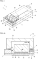
FIG. 3 is a perspective view of the light-emitting device 1. -
FIG. 4A is a cross-sectional view of a light-emitting device 1a according to a second embodiment. -
FIG. 4B is a plan view of the light-emitting device 1a illustrating its internal structure. -
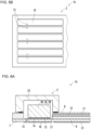
FIG. 5A is a cross-sectional view of a light-emitting device 1b according to a fourth embodiment. -
FIG. 5B is a bottom view of the light-emittingdevice 1b. -
FIG. 6A is a cross-sectional view of a light-emitting device 1b with an example structure similar to the structure according to the fourth embodiment. -
FIG. 6B is a bottom view of the light-emittingdevice 1b. -
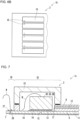
FIG. 7 is a partial cross-sectional view of a light-emitting device 1c according to a fifth embodiment. -
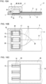
FIG. 8A is a cross-sectional view of a light-emitting device 1d according to a sixth embodiment. -
FIG. 8B is a plan view of the light-emittingdevice 1d without alid 23. -
FIG. 8C is a bottom view of the light-emitting device 1d. -
FIG. 9A is a cross-sectional view of a light-emittingdevice 1e according to a seventh embodiment. -
FIG. 9B is a plan view of the light-emittingdevice 1e without thelid 23. -
FIG. 9C is a bottom view of the light-emitting device 1e. -
FIG. 10A is a cross-sectional view of a light-emittingdevice 1f according to an eighth embodiment. -
FIG. 10B is a plan view of the light-emittingdevice 1f without thelid 23. -
FIG. 10C is a bottom view of the light-emittingdevice 1f. -
FIG. 11A is a cross-sectional view of a light-emittingdevice 1g according to a ninth embodiment. -
FIG. 11B is a plan view of the light-emittingdevice 1g without thelid 23. -
FIG. 11C is a bottom view of the light-emitting device 1g. -
FIG. 12A is a cross-sectional view of a light-emittingdevice 1h according to a tenth embodiment. -
FIG. 12B is a plan view of the light-emittingdevice 1h without thelid 23. -
FIG. 12C is a bottom view of the light-emittingdevice 1h. -
FIG. 13 is a cross-sectional view of a light-emitting device 1i according to an eleventh embodiment. - The structure that forms the basis of an optical waveguide package according to one or more embodiments of the present disclosure and a light-emitting device including the optical waveguide package includes an optical integrated circuit including a gas-barrier optical waveguide including a non gas-barrier core and a non gas-barrier cladding having a permeability coefficient for helium lower than or equal to 5 × 10⁻⁹ cm3(STP)mm/(cm2·sec·cmHg) (25 °C) coated with a gas-barrier thin film, a gas-barrier cap, an optical element including a light receiver or a light emitter mounted on a first surface of the optical waveguide at a position to be optically coupled to the core, and a metal wiring member on the first surface of the waveguide and direct below the thin film to be electrically connected to the optical element on the first surface of the optical waveguide.
- To mount the optical waveguide and the cap on the optical integrated circuit, the thin film on the first surface of the optical waveguide and on the metal wiring member and a second surface of the cap are joined together with a gas-barrier inorganic material layer in between, without an organic material layer, to achieve gas-barrier performance. A sealed airtight space is defined by the thin film on the optical waveguide and the gas-barrier members alone. The sealed airtight space accommodates one end of the core and the optical element.
- An optical waveguide package and a light-emitting device according to one or more embodiments of the present disclosure will now be described with reference to the drawings. The figures referred to below are schematic diagrams illustrating main components of the optical waveguide package and the light-emitting device for ease of illustration. The optical waveguide package and the light-emitting device may include known components not illustrated in the figures, such as circuit boards, wire conductors, control ICs, or LSIs. In the embodiments described below, the same reference numerals denote the corresponding components and will not be described repeatedly.
-
FIG. 1 is a cross-sectional view of a light-emittingdevice 1 including anoptical waveguide package 2 according to a first embodiment.FIG. 2 is a plan view of the light-emittingdevice 1.FIG. 3 is a perspective view of the light-emittingdevice 1. In the present embodiment, the light-emittingdevice 1 includes theoptical waveguide package 2, light-emittingelements condenser lens 4. - The
optical waveguide package 2 includes asubstrate 7 including afirst surface 5 and asecond surface 6 opposite to thefirst surface 5, acladding 11 located on thesecond surface 6 and including athird surface 8 facing thesecond surface 6, afourth surface 9 opposite to thethird surface 8, and an element-receivingportion 10 with openings in thefourth surface 9, a core 12 located in thecladding 11 and extending from the element-receivingportion 10, andfirst metal members 14 located in the element-receivingportion 10 in a plan view as viewed in a direction toward thefourth surface 9 and each including anelement mount 13. - The
substrate 7 may be a ceramic board including dielectric layers made of a ceramic material. Examples of the ceramic material used for the ceramic board include sintered aluminum oxide, sintered mullite, sintered silicon carbide, sintered aluminum nitride, and sintered glass ceramic. For thesubstrate 7 being a ceramic board, the dielectric layers include conductors such as connection pads, internal wiring conductors, and external connection terminals for electrical connection between the light-emittingelements - The
substrate 7 may be an organic board including dielectric layers made of an organic material. The organic board may be a printed board, a build-up board, or a flexible board. Examples of the organic material used for the organic board include an epoxy resin, a polyimide resin, a polyester resin, an acrylic resin, a phenolic resin, and a fluororesin. - The
core 12 is located in thecladding 11. Thecore 12 and thecladding 11 form an optical waveguide. Both thecore 12 and thecladding 11 may be glass or a resin. In some embodiments, one of thecore 12 and thecladding 11 may be glass, and the other may be a resin. In this case, thecore 12 and thecladding 11 have different refractive indexes, or specifically, thecore 12 has a higher refractive index than thecladding 11. The difference in the refractive index causes total internal reflection of light. More specifically, a material with a higher refractive index is used for an optical path, which is then surrounded by a material with a lower refractive index. This structure confines and carries light in the core 12 with the higher refractive index. - The
core 12 includes multiple incident end faces 17 and oneemission end face 18. Thecore 12 defines, between the incident end faces 17 and theemission end face 18, a merging path including multiple branchingpaths 19, a mergingportion 20, and a joinedpath 21. The branchingpaths 19 include the corresponding incident end faces 17 at one end. The mergingportion 20 merges the branchingpaths 19 together. The joinedpath 21 includes the emission end face 18 at one end. - The
condenser lens 4 faces the emission end face 18 of thecore 12 and aside surface 22 of thesubstrate 7 adjacent to theemission end face 18. Thecondenser lens 4 may be, for example, a lens such as a SELFOC (registered trademark) lens or a rod lens, or an optical element such as a diffraction grating. Thecondenser lens 4 has an optical axis aligned with the central axis of theemission end face 18. Thecondenser lens 4, which is an optical member, may face at least a portion of the emission end face 18 of thecore 12 and theside surface 22 of thesubstrate 7 adjacent to theemission end face 18. In other words, thecondenser lens 4 may be on an optical path of the light emitted from thecore 12. - Red (R) light, green (G) light, and blue (B) light emitted from the respective light-emitting
elements paths 19 through the incident end faces 17 and pass through the mergingportion 20 and the joinedpath 21 to thecondenser lens 4, through which the light is condensed and emitted. - The
condenser lens 4 is, for example, a plano-convex lens with a flat incident surface and a convex emission surface. Theoptical waveguide package 2 includes an optical waveguide layer, the light-emittingelements condenser lens 4 assembled together to align the optical axis of each branchingpath 19 with the center of a light emitter in the corresponding light-emittingelement - The
cladding 11 includes recesses each defined by a bottom surface and inner wall surfaces surrounding the bottom surface. The recesses serve as the element-receivingportion 10. The recesses may extend to thethird surface 8 and to thesecond surface 6. Alid 23 is placed to cover the element-receivingportion 10. The element-receivingportion 10 extends from thefourth surface 9 to thethird surface 8. Thelid 23 is a component recessed downward and is sized to cover the element-receivingportion 10 and can receive wiring members W used for wire bonding. Thelid 23 may be formed by wet etching, dry etching, sandblasting, or another method. -
First metal members 14 each are connected to asecond metal member 16 with a first viaconductor 15 extending through thesubstrate 7 from thefirst surface 5 to thesecond surface 6 of thesubstrate 7. This structure allows connection to a power supply through secondary mounting and eliminates complicated conductor stacking between thelid 23 and thecladding 11 as well as extra processes for such complicated conductor stacking. This structure also achieves electrical connection while providing sufficient airtightness and electrical insulation. Theoptical waveguide package 2 includes fewer junctions and leads and is thus smaller. -
FIG. 4A is a cross-sectional view of a light-emitting device 1a according to a second embodiment.FIG. 4B is a plan view of the light-emitting device 1a illustrating its internal structure. The same reference numerals denote the components corresponding to those in the above embodiment and will not be described repeatedly. In the light-emitting device 1a according to the present embodiment, eachfirst metal member 14 includes afirst area 14a, which is theelement mount 13, and asecond area 14b other than thefirst area 14a. Each first viaconductor 15 is in contact with the correspondingfirst metal member 14 on thesecond area 14b. - The light-emitting
elements conductors 15 are located to avoid thefirst areas 14a, which are the element mounts 13, or more specifically, when the first viaconductors 15 are located on the correspondingsecond areas 14b. A portion including a via conductor may be surrounded by a portion protruding or recessed from the surface of the substrate. However, the first viaconductors 15 located to avoid the element mounts 13 allows highly accurate positioning of the light-emittingelements elements - The
first metal members 14 in an embodiment are located in the openings alone in a plan view as viewed in a direction toward thefourth surface 9. This structure is used for the reasons below. When themetal members 14 extend onto thethird surface 8 between thecladding 11 and thesubstrate 7, the light-emitting device is taller by the thickness of themetal members 14, and portions of eachmetal member 14 with and without thecladding 11 are to have different thermal contraction rates. Such a difference in thermal contraction may cause deformation of the entire module, separation between thecladding 11 and themetal members 14 or between themetal members 14 and thesubstrate 7, or cracks in thecladding 11. When thefirst metal members 14 are located in the openings alone, the light-emitting device is less tall and may be less susceptible to thermal contraction. -
FIG. 5A is a cross-sectional view of a light-emittingdevice 1b according to a fourth embodiment.FIG. 5B is a bottom view of the light-emittingdevice 1b.FIG. 6A is a cross-sectional view of a light-emittingdevice 1b with an example structure similar to the structure according to the fourth embodiment.FIG. 6B is a bottom view of the light-emittingdevice 1b. The same reference numerals denote the components corresponding to those in the above embodiments and will not be described repeatedly. In the light-emittingdevice 1b according to the present embodiment,second metal members 16 are larger than thefirst metal members 14 in a transparent bottom view as viewed through in a direction toward thefourth surface 9. In the present embodiment, thesecond metal members 16 are elongated in the longitudinal direction of the substrate 7 (the lateral direction inFIGs. 5A ,5B ,6A , and6B ). Thesecond metal members 16 being longer and thus larger than thefirst metal members 14 simplifies secondary mounting to an external circuit and improves heat dissipation. -
FIG. 7 is a partial cross-sectional view of a light-emittingdevice 1c according to a fifth embodiment. The same reference numerals denote the components corresponding to those in the above embodiments and will not be described repeatedly. In the light-emittingdevice 1c according to the present embodiment, thesecond surface 6 includes athird area 25 inward from the outer periphery of thecladding 11 and afourth area 26 other than thethird area 25.Third metal members 27 are located in thefourth area 26. Eachthird metal member 27 is connected to the correspondingsecond metal member 16 with a second viaconductor 28 extending through thesubstrate 7 from thefirst surface 5 to thesecond surface 6 of thesubstrate 7. - This structure allows formation of lead electrodes on the surface without separating the
lid 23 and thecladding 11. Thethird metal members 27 on the externalfourth area 26 may be easily connected to an external power supply with the wiring members W. -
FIG. 8A is a cross-sectional view of a light-emittingdevice 1d according to a sixth embodiment.FIG. 8B is a plan view of the light-emittingdevice 1d without thelid 23.FIG. 8C is a bottom view of the light-emittingdevice 1d. The same reference numerals denote the components corresponding to those in the above embodiments and will not be described repeatedly. In the light-emittingdevice 1d according to the present embodiment,first metal members 14 andsecond metal members 16 have the same shape and are plane symmetrical with respect to a plane parallel to thefirst surface 5. This structure has higher symmetry in the vertical direction inFIG. 8A in a side view and reduces deformation directly below the element mounts 13. -
FIG. 9A is a cross-sectional view of a light-emittingdevice 1e according to a seventh embodiment.FIG. 9B is a plan view of the light-emittingdevice 1e without thelid 23.FIG. 9C is a bottom view of the light-emittingdevice 1e. The same reference numerals denote the components corresponding to those in the above embodiments and will not be described repeatedly. In the light-emittingdevice 1e according to the present embodiment,second metal members 16 located on thefirst surface 5 include surfaces opposite to their surfaces facing thefirst surface 5 that are flat, or in other words, form a flat surface. This structure reduces tilt during secondary mounting, allows mounting of the light-emittingdevice 1e in a leveler state, and stabilizes secondary mounting to an external circuit. -
FIG. 10A is a cross-sectional view of a light-emittingdevice 1f according to an eighth embodiment.FIG. 10B is a plan view of the light-emittingdevice 1f without thelid 23.FIG. 10C is a bottom view of the light-emittingdevice 1f. The same reference numerals denote the components corresponding to those in the above embodiments and will not be described repeatedly. In the light-emittingdevice 1f according to the present embodiment,second metal members 16 located on thefirst surface 5 include surfaces opposite to their surfaces facing thefirst surface 5 that are flat, or in other words, form a flat surface. Thefirst surface 5 includes afifth area 29 in which thesecond metal members 16 are located and asixth area 30 other than thefifth area 29. Afourth metal member 31 is located on thesixth area 30. Thefourth metal member 31 includes a surface opposite to its surface facing thefirst surface 5 that is flat similarly to thesecond metal members 16, or in other words, is formed on a common flat surface including the surfaces of thesecond metal members 16. This structure simplifies the manufacturing processes by allowing formation of thesecond metal members 16 and thefourth metal member 31 at the same time, and improves heat dissipation. -
FIG. 11A is a cross-sectional view of a light-emittingdevice 1g according to a ninth embodiment.FIG. 11B is a plan view of the light-emittingdevice 1g without thelid 23.FIG. 11C is a bottom view of the light-emittingdevice 1g. The same reference numerals denote the components corresponding to those in the above embodiments and will not be described repeatedly. In the light-emittingdevice 1g according to the present embodiment, thesecond metal members 16 are located on thefirst surface 5. Thefirst surface 5 includes thefifth area 29 in which thesecond metal members 16 are located and thesixth area 30 other than thefifth area 29.Fourth metal members 31 are located in thefourth area 26. Thesecond metal members 16 and thefourth metal members 31 are line symmetrical with respect to a central line L1 including the center of thefirst surface 5. This structure reduces asymmetric distribution of deformation with respect to the central line L1 due to higher temperatures of thesecond metal members 16 and thefourth metal members 31, and thus generates less thermal stress. -
FIG. 12A is a cross-sectional view of a light-emittingdevice 1h according to a tenth embodiment.FIG. 12B is a plan view of the light-emittingdevice 1h without thelid 23.FIG. 12C is a bottom view of the light-emittingdevice 1h. The same reference numerals denote the components corresponding to those in the above embodiments and will not be described repeatedly. In the light-emittingdevice 1h according to the present embodiment, a contact area between each first viaconductor 15 and the correspondingsecond area 14b is larger than or as large as the correspondingfirst area 14a. This structure increases the efficiency of heat transfer from thefirst metal members 14 located inside to the correspondingsecond metal members 16 located outside, and improves heat dissipation. -
FIG. 13 is a cross-sectional view of a light-emitting device 1i according to an eleventh embodiment. The same reference numerals denote the components corresponding to those in the above embodiments and will not be described repeatedly. In the present embodiment, the light-emittingdevice 1 includes thelid 23 sealing the element-receivingportion 10. Thelid 23 can prevent unintended entry of external light through the incident end faces 17 of thecore 12. With entry of unintended water and gas also being less likely, the light-emittingelements lid 23 with airtight sealing is particularly effective. With thelid 23 sealing the element-receivingportion 10, foreign matter such as objects suspended in the air are less likely to enter the element-receivingportion 10. This reduces objects that block traveling light in a space between the emission end of each light-emittingelement incident end face 17 of thecore 12. - In another example similar to the eleventh embodiment, a light-emitting device 1i includes a
metal layer 33, which is, for example, a soldered bonding layer made of AuSn, SnAgCu, or another material, between the element-receivingportion 10 and thelid 23. Themetal layer 33 airtightly joins thelid 23 and thecladding 11 together to seal the element-receivingportion 10 as described above. - In still another embodiment of the present disclosure, the light-emitting
elements - The present disclosure may be implemented in the following forms.
- In one or more embodiments of the present disclosure, an optical waveguide package includes a substrate including a first surface and a second surface opposite to the first surface, a cladding located on the second surface and including a third surface facing the second surface, a fourth surface opposite to the third surface, and an element-receiving portion with an opening in the fourth surface, a core located in the cladding and extending from the element-receiving portion, and a first metal member located in the element-receiving portion in a plan view as viewed in a direction toward the fourth surface and including an element mount. The first metal member is connected to a second metal member with a first via conductor extending through the substrate from the first surface to the second surface.
- In one or more embodiments of the present disclosure, a light-emitting device includes the optical waveguide package according to the above embodiments, a light-emitting element connected to the first metal member, and a lens on an optical path of light emitted from the core.
- In one or more embodiments of the present disclosure, the optical waveguide package includes a simple connection structure to achieve high insulation at a low manufacturing cost.
- In one or more embodiments of the present disclosure, the light-emitting device includes a simple connection structure to achieve high insulation at a low manufacturing cost.
- Although embodiments of the present disclosure have been described in detail, the present disclosure is not limited to the embodiments described above, and may be changed or varied in various manners without departing from the spirit and scope of the present disclosure. The components described in the above embodiments may be entirely or partially combined as appropriate unless any contradiction arises.
-
- 1, 1a to 1i
- light-emitting device
- 2
- optical waveguide package
- 3R, 3G, 3B
- light-emitting element
- 4
- condenser lens
- 5
- first surface
- 6
- second surface
- 7
- substrate
- 8
- third surface
- 9
- fourth surface
- 10
- element-receiving portion
- 11
- cladding
- 12
- core
- 13
- element mount
- 14
- first metal member
- 15
- first via conductor
- 16
- second metal member
- 17
- incident end face
- 18
- emission end face
- 19
- branching path
- 20
- merging portion
- 21
- joined path
- 22
- side surface
- 23
- lid
- 25
- third area
- 26
- fourth area
- 27
- third metal member
- 28
- second via conductor
- 29
- fifth area
- 30
- sixth area
- 31
- fourth metal member
- 33
- metal layer
Claims (15)
- An optical waveguide package, comprising:a substrate including a first surface and a second surface opposite to the first surface;a cladding on the second surface, the cladding including a third surface facing the second surface, a fourth surface opposite to the third surface, and an element-receiving portion with an opening in the fourth surface;a core in the cladding, the core extending from the element-receiving portion; anda first metal member in the element-receiving portion in a plan view as viewed in a direction toward the fourth surface, the first metal member including an element mount,wherein the first metal member is connected to a second metal member with a first via conductor extending through the substrate from the first surface to the second surface.
- The optical waveguide package according to claim 1, wherein
the element-receiving portion extends from the fourth surface to the third surface. - The optical waveguide package according to claim 1 or claim 2, whereinthe first metal member includes a first area being the element mount and a second area other than the first area, andthe first via conductor is in contact with the second area.
- The optical waveguide package according to any one of claims 1 to 3, wherein
the first metal member is located in the opening alone in the plan view. - The optical waveguide package according to any one of claims 1 to 4, wherein
the second metal member is larger than the first metal member in a transparent plan view as viewed through in a direction toward the fourth surface. - The optical waveguide package according to claim 5, whereinthe second surface includes a third area inward from an outer periphery of the cladding and a fourth area other than the third area,the optical waveguide package further includes a third metal member located in the fourth area, andthe third metal member is connected to the second metal member with a second via conductor extending through the substrate from the first surface to the second surface.
- The optical waveguide package according to any one of claims 1 to 4, wherein
the first metal member and the second metal member have a same shape and are plane symmetrical with respect to the first surface. - The optical waveguide package according to any one of claims 1 to 7, wherein
the second metal member is on the first surface, and the second metal member includes a flat surface opposite to a surface facing the first surface. - The optical waveguide package according to any one of claims 1 to 8, whereinthe second metal member is on the first surface, and the second metal member includes a surface opposite to a flat surface facing the first surface,the first surface includes a fifth area in which the second metal member is located and a sixth area other than the fifth area,the optical waveguide package further includes a fourth metal member in the sixth area, andthe fourth metal member includes, similarly to the second metal member, a flat surface opposite to a surface facing the first surface.
- The optical waveguide package according to any one of claims 1 to 9, whereinthe second metal member is on the first surface,the first surface includes a fifth area in which the second metal member is located and a sixth area other than the fifth area,the optical waveguide package further includes a fourth metal member in the fourth area, andthe second metal member and the fourth metal member are line symmetrical with respect to a central line including a center of the first surface.
- The optical waveguide package according to claim 3, wherein
a contact area between the first via conductor and the second area is larger than or as large as the first area. - The optical waveguide package according to any one of claims 1 to 11, further comprising:
a lid sealing the element-receiving portion. - The optical waveguide package according to claim 12, further comprising:
a metal layer between the element-receiving portion and the lid. - A light-emitting device, comprising:the optical waveguide package according to any one of claims 1 to 13;a light-emitting element connected to the first metal member; anda lens on an optical path of light emitted from the core.
- The light-emitting device according to claim 14, whereinthe lid includes a recess, andthe light-emitting element extends from the element-receiving portion into the recess.
Applications Claiming Priority (2)
| Application Number | Priority Date | Filing Date | Title |
|---|---|---|---|
| JP2020094753 | 2020-05-29 | ||
| PCT/JP2021/018825 WO2021241332A1 (en) | 2020-05-29 | 2021-05-18 | Optical waveguide package and light emitting device |
Publications (3)
| Publication Number | Publication Date |
|---|---|
| EP4160705A1 true EP4160705A1 (en) | 2023-04-05 |
| EP4160705A4 EP4160705A4 (en) | 2024-07-10 |
| EP4160705B1 EP4160705B1 (en) | 2026-05-06 |
Family
ID=78744541
Family Applications (1)
| Application Number | Title | Priority Date | Filing Date |
|---|---|---|---|
| EP21812397.4A Active EP4160705B1 (en) | 2020-05-29 | 2021-05-18 | Optical waveguide package and light emitting device |
Country Status (5)
| Country | Link |
|---|---|
| US (1) | US20230213699A1 (en) |
| EP (1) | EP4160705B1 (en) |
| JP (1) | JP7431958B2 (en) |
| CN (1) | CN115668669A (en) |
| WO (1) | WO2021241332A1 (en) |
Families Citing this family (2)
| Publication number | Priority date | Publication date | Assignee | Title |
|---|---|---|---|---|
| CN117369059A (en) * | 2022-06-30 | 2024-01-09 | 成都旭创科技有限公司 | Optical devices and optical modules for optical communications |
| DE102024110364A1 (en) * | 2024-04-12 | 2025-10-16 | Ams-Osram International Gmbh | OPTOELECTRONIC ARRANGEMENT AND METHOD FOR SHAPING A LASER LIGHT EMISSED BY A SEMICONDUCTOR LASER DEVICE OF AN OPTOELECTRONIC ARRANGEMENT |
Family Cites Families (16)
| Publication number | Priority date | Publication date | Assignee | Title |
|---|---|---|---|---|
| US5521992A (en) * | 1994-08-01 | 1996-05-28 | Motorola, Inc. | Molded optical interconnect |
| JPH0961651A (en) * | 1995-06-14 | 1997-03-07 | Nippon Telegr & Teleph Corp <Ntt> | Hybrid optical integrated circuit |
| JPH10308555A (en) * | 1997-05-01 | 1998-11-17 | Nippon Telegr & Teleph Corp <Ntt> | Hybrid waveguide type optical circuit and manufacturing method thereof |
| JP3728147B2 (en) * | 1999-07-16 | 2005-12-21 | キヤノン株式会社 | Opto-electric hybrid wiring board |
| CN100358148C (en) * | 2001-12-19 | 2007-12-26 | 松下电器产业株式会社 | Optical module |
| CN101351733B (en) * | 2005-12-28 | 2011-03-30 | 欧姆龙株式会社 | Optical module |
| JP4579868B2 (en) * | 2006-06-08 | 2010-11-10 | 日本電信電話株式会社 | Optical integrated circuit |
| JP5549104B2 (en) | 2008-05-29 | 2014-07-16 | 株式会社リコー | Light emitting device, optical scanning device, and image forming apparatus |
| JP5679117B2 (en) * | 2011-03-09 | 2015-03-04 | セイコーエプソン株式会社 | Light emitting device, irradiation device, and projector |
| US9057850B2 (en) * | 2011-03-24 | 2015-06-16 | Centera Photonics Inc. | Optoelectronic module |
| CN103250240B (en) * | 2011-05-31 | 2016-01-06 | 京瓷株式会社 | Element storage encapsulation, member for semiconductor device and semiconductor device |
| JP6437875B2 (en) * | 2015-04-21 | 2018-12-12 | 新光電気工業株式会社 | Optical waveguide device and manufacturing method thereof |
| CN108140689A (en) * | 2015-12-10 | 2018-06-08 | 京瓷株式会社 | Sensor substrate and sensor device |
| RU2019106302A (en) * | 2016-08-10 | 2020-09-16 | Киосера Корпорейшн | ELECTRIC ELEMENT MOUNTING HOUSING, MATRIX HOUSING AND ELECTRICAL DEVICE |
| US10551561B2 (en) * | 2018-01-25 | 2020-02-04 | Poet Technologies, Inc. | Optical dielectric waveguide structures |
| DE102018102961B4 (en) | 2018-02-09 | 2025-05-08 | Msg Lithoglas Gmbh | Component arrangement, package and package arrangement and method for manufacturing |
-
2021
- 2021-05-18 EP EP21812397.4A patent/EP4160705B1/en active Active
- 2021-05-18 US US17/927,656 patent/US20230213699A1/en active Pending
- 2021-05-18 JP JP2022526917A patent/JP7431958B2/en active Active
- 2021-05-18 CN CN202180036723.5A patent/CN115668669A/en active Pending
- 2021-05-18 WO PCT/JP2021/018825 patent/WO2021241332A1/en not_active Ceased
Also Published As
| Publication number | Publication date |
|---|---|
| CN115668669A (en) | 2023-01-31 |
| EP4160705B1 (en) | 2026-05-06 |
| JP7431958B2 (en) | 2024-02-15 |
| JPWO2021241332A1 (en) | 2021-12-02 |
| US20230213699A1 (en) | 2023-07-06 |
| WO2021241332A1 (en) | 2021-12-02 |
| EP4160705A4 (en) | 2024-07-10 |
Similar Documents
| Publication | Publication Date | Title |
|---|---|---|
| US12181723B2 (en) | Optical waveguide package and light-emitting device | |
| US9835297B2 (en) | Light emitting device having a wavelength converter fixed to the mounting surface | |
| US9893259B2 (en) | Light emitting package | |
| EP4040515A1 (en) | Optical waveguide package and light emitting device | |
| US20220390689A1 (en) | Optical waveguide package and light-emitting device | |
| JP6048880B2 (en) | LIGHT EMITTING ELEMENT PACKAGE AND LIGHT EMITTING DEVICE USING THE SAME | |
| EP4160705B1 (en) | Optical waveguide package and light emitting device | |
| US20240204476A1 (en) | Optoelectronic semiconductor component | |
| KR20100099734A (en) | Compact housing | |
| CN113394654A (en) | Laser device | |
| CN216162111U (en) | Laser device | |
| US12124079B2 (en) | Optical waveguide package and light-emitting device | |
| US12222540B2 (en) | Optical waveguide package and light-emitting device | |
| EP4478098A1 (en) | Optical waveguide substrate, optical waveguide package, and light source module | |
| JPWO2021241332A5 (en) | ||
| JPWO2020162023A1 (en) | Semiconductor light emitting device | |
| EP4297206A1 (en) | Light emitting device | |
| US20240272379A1 (en) | Optical waveguide package and light-emitting device | |
| US20250023001A1 (en) | Optical waveguide package and light-emitting device | |
| JP7217692B2 (en) | Optical waveguide package and light emitting device | |
| US20250306319A1 (en) | Optical waveguide package and light-emitting device | |
| US12620772B2 (en) | Light emitting device | |
| JP2019153570A (en) | Light emitting module | |
| US20230344192A1 (en) | Light emitting device | |
| JP6910976B2 (en) | Optical module |
Legal Events
| Date | Code | Title | Description |
|---|---|---|---|
| STAA | Information on the status of an ep patent application or granted ep patent |
Free format text: STATUS: THE INTERNATIONAL PUBLICATION HAS BEEN MADE |
|
| PUAI | Public reference made under article 153(3) epc to a published international application that has entered the european phase |
Free format text: ORIGINAL CODE: 0009012 |
|
| STAA | Information on the status of an ep patent application or granted ep patent |
Free format text: STATUS: REQUEST FOR EXAMINATION WAS MADE |
|
| 17P | Request for examination filed |
Effective date: 20221123 |
|
| AK | Designated contracting states |
Kind code of ref document: A1 Designated state(s): AL AT BE BG CH CY CZ DE DK EE ES FI FR GB GR HR HU IE IS IT LI LT LU LV MC MK MT NL NO PL PT RO RS SE SI SK SM TR |
|
| P01 | Opt-out of the competence of the unified patent court (upc) registered |
Effective date: 20230505 |
|
| DAV | Request for validation of the european patent (deleted) | ||
| DAX | Request for extension of the european patent (deleted) | ||
| A4 | Supplementary search report drawn up and despatched |
Effective date: 20240607 |
|
| RIC1 | Information provided on ipc code assigned before grant |
Ipc: H01S 5/022 20210101ALI20240603BHEP Ipc: G02B 6/42 20060101ALI20240603BHEP Ipc: H01L 33/62 20100101AFI20240603BHEP |
|
| REG | Reference to a national code |
Ref country code: DE Ref legal event code: R079 Free format text: PREVIOUS MAIN CLASS: H01L0033620000 Ipc: G02B0006420000 Ref country code: DE Ref legal event code: R079 Ref document number: 602021053919 Country of ref document: DE Free format text: PREVIOUS MAIN CLASS: H01L0033620000 Ipc: G02B0006420000 |
|
| GRAP | Despatch of communication of intention to grant a patent |
Free format text: ORIGINAL CODE: EPIDOSNIGR1 |
|
| STAA | Information on the status of an ep patent application or granted ep patent |
Free format text: STATUS: GRANT OF PATENT IS INTENDED |
|
| RIC1 | Information provided on ipc code assigned before grant |
Ipc: G02B 6/42 20060101AFI20251126BHEP Ipc: H01S 5/022 20210101ALI20251126BHEP |
|
| INTG | Intention to grant announced |
Effective date: 20251210 |
|
| GRAS | Grant fee paid |
Free format text: ORIGINAL CODE: EPIDOSNIGR3 |
|
| GRAA | (expected) grant |
Free format text: ORIGINAL CODE: 0009210 |
|
| STAA | Information on the status of an ep patent application or granted ep patent |
Free format text: STATUS: THE PATENT HAS BEEN GRANTED |