EP4160694A1 - Method for manufacturing a quantum electronic circuit - Google Patents
Method for manufacturing a quantum electronic circuit Download PDFInfo
- Publication number
- EP4160694A1 EP4160694A1 EP22198944.5A EP22198944A EP4160694A1 EP 4160694 A1 EP4160694 A1 EP 4160694A1 EP 22198944 A EP22198944 A EP 22198944A EP 4160694 A1 EP4160694 A1 EP 4160694A1
- Authority
- EP
- European Patent Office
- Prior art keywords
- layer
- plr
- semiconductor
- dielectric
- pillar
- Prior art date
- Legal status (The legal status is an assumption and is not a legal conclusion. Google has not performed a legal analysis and makes no representation as to the accuracy of the status listed.)
- Pending
Links
- 238000000034 method Methods 0.000 title claims abstract description 74
- 238000004519 manufacturing process Methods 0.000 title claims abstract description 27
- 239000004065 semiconductor Substances 0.000 claims abstract description 164
- 230000008878 coupling Effects 0.000 claims abstract description 109
- 238000010168 coupling process Methods 0.000 claims abstract description 109
- 238000005859 coupling reaction Methods 0.000 claims abstract description 109
- 238000000926 separation method Methods 0.000 claims abstract description 100
- 238000005530 etching Methods 0.000 claims abstract description 84
- 239000002096 quantum dot Substances 0.000 claims abstract description 77
- 238000000151 deposition Methods 0.000 claims abstract description 46
- 230000001590 oxidative effect Effects 0.000 claims abstract description 6
- 230000015572 biosynthetic process Effects 0.000 claims description 40
- 230000001681 protective effect Effects 0.000 claims description 32
- 238000007254 oxidation reaction Methods 0.000 claims description 23
- 239000003989 dielectric material Substances 0.000 claims description 21
- 230000003647 oxidation Effects 0.000 claims description 21
- 238000000407 epitaxy Methods 0.000 claims description 13
- 239000000758 substrate Substances 0.000 claims description 11
- 239000013078 crystal Substances 0.000 claims description 8
- 229910052710 silicon Inorganic materials 0.000 claims description 7
- 239000010703 silicon Substances 0.000 claims description 7
- 229910021420 polycrystalline silicon Inorganic materials 0.000 claims description 5
- 102100036962 5'-3' exoribonuclease 1 Human genes 0.000 abstract description 27
- 101000804879 Homo sapiens 5'-3' exoribonuclease 1 Proteins 0.000 abstract description 27
- 101000654664 Homo sapiens Neuronal-specific septin-3 Proteins 0.000 abstract description 26
- 102100032769 Neuronal-specific septin-3 Human genes 0.000 abstract description 26
- 101000632314 Homo sapiens Septin-6 Proteins 0.000 abstract description 21
- 101000632054 Homo sapiens Septin-8 Proteins 0.000 abstract description 21
- 102100027982 Septin-6 Human genes 0.000 abstract description 21
- 238000003860 storage Methods 0.000 abstract description 3
- 230000008021 deposition Effects 0.000 description 29
- 101100378610 Arabidopsis thaliana AGL3 gene Proteins 0.000 description 14
- 102100032743 Septin-4 Human genes 0.000 description 14
- 101150117471 Septin4 gene Proteins 0.000 description 14
- 239000011347 resin Substances 0.000 description 10
- 229920005989 resin Polymers 0.000 description 10
- XUIMIQQOPSSXEZ-UHFFFAOYSA-N Silicon Chemical compound [Si] XUIMIQQOPSSXEZ-UHFFFAOYSA-N 0.000 description 9
- 239000000463 material Substances 0.000 description 9
- 229920008347 Cellulose acetate propionate Polymers 0.000 description 8
- 238000009470 controlled atmosphere packaging Methods 0.000 description 8
- 101001129812 Forsythia intermedia Bifunctional pinoresinol-lariciresinol reductase Proteins 0.000 description 6
- VYPSYNLAJGMNEJ-UHFFFAOYSA-N Silicium dioxide Chemical compound O=[Si]=O VYPSYNLAJGMNEJ-UHFFFAOYSA-N 0.000 description 6
- 238000000206 photolithography Methods 0.000 description 6
- 229910052814 silicon oxide Inorganic materials 0.000 description 6
- 229910004298 SiO 2 Inorganic materials 0.000 description 5
- 230000007547 defect Effects 0.000 description 5
- 238000005538 encapsulation Methods 0.000 description 5
- 238000005259 measurement Methods 0.000 description 5
- 101100243965 Arabidopsis thaliana PRR1 gene Proteins 0.000 description 4
- 229910052796 boron Inorganic materials 0.000 description 4
- 101150103743 plr1 gene Proteins 0.000 description 4
- 101100243972 Arabidopsis thaliana PRR2 gene Proteins 0.000 description 3
- 229910052581 Si3N4 Inorganic materials 0.000 description 3
- 238000003491 array Methods 0.000 description 3
- 230000005686 electrostatic field Effects 0.000 description 3
- 229910021332 silicide Inorganic materials 0.000 description 3
- FVBUAEGBCNSCDD-UHFFFAOYSA-N silicide(4-) Chemical compound [Si-4] FVBUAEGBCNSCDD-UHFFFAOYSA-N 0.000 description 3
- HQVNEWCFYHHQES-UHFFFAOYSA-N silicon nitride Chemical compound N12[Si]34N5[Si]62N3[Si]51N64 HQVNEWCFYHHQES-UHFFFAOYSA-N 0.000 description 3
- XUIMIQQOPSSXEZ-IGMARMGPSA-N silicon-28 atom Chemical compound [28Si] XUIMIQQOPSSXEZ-IGMARMGPSA-N 0.000 description 3
- 101100366322 Arabidopsis thaliana ADC1 gene Proteins 0.000 description 2
- KRHYYFGTRYWZRS-UHFFFAOYSA-N Fluorane Chemical compound F KRHYYFGTRYWZRS-UHFFFAOYSA-N 0.000 description 2
- NBIIXXVUZAFLBC-UHFFFAOYSA-N Phosphoric acid Chemical compound OP(O)(O)=O NBIIXXVUZAFLBC-UHFFFAOYSA-N 0.000 description 2
- 101150032645 SPE1 gene Proteins 0.000 description 2
- 229910000577 Silicon-germanium Inorganic materials 0.000 description 2
- NRTOMJZYCJJWKI-UHFFFAOYSA-N Titanium nitride Chemical compound [Ti]#N NRTOMJZYCJJWKI-UHFFFAOYSA-N 0.000 description 2
- 239000002800 charge carrier Substances 0.000 description 2
- 239000004020 conductor Substances 0.000 description 2
- 238000011161 development Methods 0.000 description 2
- 230000000694 effects Effects 0.000 description 2
- 238000010292 electrical insulation Methods 0.000 description 2
- 229910052732 germanium Inorganic materials 0.000 description 2
- GNPVGFCGXDBREM-UHFFFAOYSA-N germanium atom Chemical compound [Ge] GNPVGFCGXDBREM-UHFFFAOYSA-N 0.000 description 2
- 239000002184 metal Substances 0.000 description 2
- 229910052751 metal Inorganic materials 0.000 description 2
- 229920005591 polysilicon Polymers 0.000 description 2
- 125000006850 spacer group Chemical group 0.000 description 2
- 239000010936 titanium Substances 0.000 description 2
- ZOXJGFHDIHLPTG-UHFFFAOYSA-N Boron Chemical compound [B] ZOXJGFHDIHLPTG-UHFFFAOYSA-N 0.000 description 1
- 102100032912 CD44 antigen Human genes 0.000 description 1
- 101000610550 Homo sapiens Opiorphin prepropeptide Proteins 0.000 description 1
- 101001002066 Homo sapiens Pleiotropic regulator 1 Proteins 0.000 description 1
- 101000830696 Homo sapiens Protein tyrosine phosphatase type IVA 1 Proteins 0.000 description 1
- OAICVXFJPJFONN-UHFFFAOYSA-N Phosphorus Chemical compound [P] OAICVXFJPJFONN-UHFFFAOYSA-N 0.000 description 1
- 102100024599 Protein tyrosine phosphatase type IVA 1 Human genes 0.000 description 1
- ATJFFYVFTNAWJD-UHFFFAOYSA-N Tin Chemical compound [Sn] ATJFFYVFTNAWJD-UHFFFAOYSA-N 0.000 description 1
- RTAQQCXQSZGOHL-UHFFFAOYSA-N Titanium Chemical compound [Ti] RTAQQCXQSZGOHL-UHFFFAOYSA-N 0.000 description 1
- BLOIXGFLXPCOGW-UHFFFAOYSA-N [Ti].[Sn] Chemical compound [Ti].[Sn] BLOIXGFLXPCOGW-UHFFFAOYSA-N 0.000 description 1
- 229910000147 aluminium phosphate Inorganic materials 0.000 description 1
- 238000005234 chemical deposition Methods 0.000 description 1
- 238000005229 chemical vapour deposition Methods 0.000 description 1
- 238000012937 correction Methods 0.000 description 1
- 230000002950 deficient Effects 0.000 description 1
- 238000000280 densification Methods 0.000 description 1
- 230000001419 dependent effect Effects 0.000 description 1
- 238000003384 imaging method Methods 0.000 description 1
- 238000009776 industrial production Methods 0.000 description 1
- 239000012212 insulator Substances 0.000 description 1
- 230000010354 integration Effects 0.000 description 1
- 108010069264 keratinocyte CD44 Proteins 0.000 description 1
- 229910021421 monocrystalline silicon Inorganic materials 0.000 description 1
- 229910052698 phosphorus Inorganic materials 0.000 description 1
- 239000011574 phosphorus Substances 0.000 description 1
- 229910052697 platinum Inorganic materials 0.000 description 1
- BASFCYQUMIYNBI-UHFFFAOYSA-N platinum Substances [Pt] BASFCYQUMIYNBI-UHFFFAOYSA-N 0.000 description 1
- -1 platinum nitride Chemical class 0.000 description 1
- 238000005498 polishing Methods 0.000 description 1
- 238000010405 reoxidation reaction Methods 0.000 description 1
- 238000004626 scanning electron microscopy Methods 0.000 description 1
- 238000001350 scanning transmission electron microscopy Methods 0.000 description 1
- 239000000126 substance Substances 0.000 description 1
- 229910052719 titanium Inorganic materials 0.000 description 1
- 238000012549 training Methods 0.000 description 1
- 230000001131 transforming effect Effects 0.000 description 1
- WFKWXMTUELFFGS-UHFFFAOYSA-N tungsten Chemical compound [W] WFKWXMTUELFFGS-UHFFFAOYSA-N 0.000 description 1
- 229910052721 tungsten Inorganic materials 0.000 description 1
- 239000010937 tungsten Substances 0.000 description 1
Images


Classifications
-
- H—ELECTRICITY
- H01—ELECTRIC ELEMENTS
- H01L—SEMICONDUCTOR DEVICES NOT COVERED BY CLASS H10
- H01L29/00—Semiconductor devices specially adapted for rectifying, amplifying, oscillating or switching and having potential barriers; Capacitors or resistors having potential barriers, e.g. a PN-junction depletion layer or carrier concentration layer; Details of semiconductor bodies or of electrodes thereof ; Multistep manufacturing processes therefor
- H01L29/02—Semiconductor bodies ; Multistep manufacturing processes therefor
- H01L29/06—Semiconductor bodies ; Multistep manufacturing processes therefor characterised by their shape; characterised by the shapes, relative sizes, or dispositions of the semiconductor regions ; characterised by the concentration or distribution of impurities within semiconductor regions
- H01L29/0657—Semiconductor bodies ; Multistep manufacturing processes therefor characterised by their shape; characterised by the shapes, relative sizes, or dispositions of the semiconductor regions ; characterised by the concentration or distribution of impurities within semiconductor regions characterised by the shape of the body
- H01L29/0665—Semiconductor bodies ; Multistep manufacturing processes therefor characterised by their shape; characterised by the shapes, relative sizes, or dispositions of the semiconductor regions ; characterised by the concentration or distribution of impurities within semiconductor regions characterised by the shape of the body the shape of the body defining a nanostructure
- H01L29/0669—Nanowires or nanotubes
- H01L29/0676—Nanowires or nanotubes oriented perpendicular or at an angle to a substrate
-
- H—ELECTRICITY
- H01—ELECTRIC ELEMENTS
- H01L—SEMICONDUCTOR DEVICES NOT COVERED BY CLASS H10
- H01L29/00—Semiconductor devices specially adapted for rectifying, amplifying, oscillating or switching and having potential barriers; Capacitors or resistors having potential barriers, e.g. a PN-junction depletion layer or carrier concentration layer; Details of semiconductor bodies or of electrodes thereof ; Multistep manufacturing processes therefor
- H01L29/66—Types of semiconductor device ; Multistep manufacturing processes therefor
- H01L29/66977—Quantum effect devices, e.g. using quantum reflection, diffraction or interference effects, i.e. Bragg- or Aharonov-Bohm effects
-
- G—PHYSICS
- G06—COMPUTING; CALCULATING OR COUNTING
- G06N—COMPUTING ARRANGEMENTS BASED ON SPECIFIC COMPUTATIONAL MODELS
- G06N10/00—Quantum computing, i.e. information processing based on quantum-mechanical phenomena
- G06N10/40—Physical realisations or architectures of quantum processors or components for manipulating qubits, e.g. qubit coupling or qubit control
-
- H—ELECTRICITY
- H01—ELECTRIC ELEMENTS
- H01L—SEMICONDUCTOR DEVICES NOT COVERED BY CLASS H10
- H01L27/00—Devices consisting of a plurality of semiconductor or other solid-state components formed in or on a common substrate
- H01L27/02—Devices consisting of a plurality of semiconductor or other solid-state components formed in or on a common substrate including semiconductor components specially adapted for rectifying, oscillating, amplifying or switching and having potential barriers; including integrated passive circuit elements having potential barriers
- H01L27/04—Devices consisting of a plurality of semiconductor or other solid-state components formed in or on a common substrate including semiconductor components specially adapted for rectifying, oscillating, amplifying or switching and having potential barriers; including integrated passive circuit elements having potential barriers the substrate being a semiconductor body
- H01L27/10—Devices consisting of a plurality of semiconductor or other solid-state components formed in or on a common substrate including semiconductor components specially adapted for rectifying, oscillating, amplifying or switching and having potential barriers; including integrated passive circuit elements having potential barriers the substrate being a semiconductor body including a plurality of individual components in a repetitive configuration
-
- H—ELECTRICITY
- H01—ELECTRIC ELEMENTS
- H01L—SEMICONDUCTOR DEVICES NOT COVERED BY CLASS H10
- H01L29/00—Semiconductor devices specially adapted for rectifying, amplifying, oscillating or switching and having potential barriers; Capacitors or resistors having potential barriers, e.g. a PN-junction depletion layer or carrier concentration layer; Details of semiconductor bodies or of electrodes thereof ; Multistep manufacturing processes therefor
- H01L29/40—Electrodes ; Multistep manufacturing processes therefor
- H01L29/41—Electrodes ; Multistep manufacturing processes therefor characterised by their shape, relative sizes or dispositions
- H01L29/423—Electrodes ; Multistep manufacturing processes therefor characterised by their shape, relative sizes or dispositions not carrying the current to be rectified, amplified or switched
-
- H—ELECTRICITY
- H01—ELECTRIC ELEMENTS
- H01L—SEMICONDUCTOR DEVICES NOT COVERED BY CLASS H10
- H01L29/00—Semiconductor devices specially adapted for rectifying, amplifying, oscillating or switching and having potential barriers; Capacitors or resistors having potential barriers, e.g. a PN-junction depletion layer or carrier concentration layer; Details of semiconductor bodies or of electrodes thereof ; Multistep manufacturing processes therefor
- H01L29/66—Types of semiconductor device ; Multistep manufacturing processes therefor
- H01L29/66007—Multistep manufacturing processes
- H01L29/66075—Multistep manufacturing processes of devices having semiconductor bodies comprising group 14 or group 13/15 materials
- H01L29/66227—Multistep manufacturing processes of devices having semiconductor bodies comprising group 14 or group 13/15 materials the devices being controllable only by the electric current supplied or the electric potential applied, to an electrode which does not carry the current to be rectified, amplified or switched, e.g. three-terminal devices
- H01L29/66409—Unipolar field-effect transistors
- H01L29/66439—Unipolar field-effect transistors with a one- or zero-dimensional channel, e.g. quantum wire FET, in-plane gate transistor [IPG], single electron transistor [SET], striped channel transistor, Coulomb blockade transistor
-
- B—PERFORMING OPERATIONS; TRANSPORTING
- B82—NANOTECHNOLOGY
- B82Y—SPECIFIC USES OR APPLICATIONS OF NANOSTRUCTURES; MEASUREMENT OR ANALYSIS OF NANOSTRUCTURES; MANUFACTURE OR TREATMENT OF NANOSTRUCTURES
- B82Y10/00—Nanotechnology for information processing, storage or transmission, e.g. quantum computing or single electron logic
-
- G—PHYSICS
- G06—COMPUTING; CALCULATING OR COUNTING
- G06N—COMPUTING ARRANGEMENTS BASED ON SPECIFIC COMPUTATIONAL MODELS
- G06N10/00—Quantum computing, i.e. information processing based on quantum-mechanical phenomena
- G06N10/70—Quantum error correction, detection or prevention, e.g. surface codes or magic state distillation
Definitions
- the technical field of the invention is that of quantum electronics and more particularly the manufacture of a quantum electronic circuit.
- Quantum electronic circuits capable of manipulating qubits include islands, also called quantum dots. Quantum dots are able to store qubits while they are being manipulated and measured.
- quantum dots in the form of quantum electronic circuits must satisfy several requirements. On the one hand, to offer a high density of quantum dots in order to offer a substantial computing capacity. On the other hand, the manufacturing methods of said quantum electronic circuits must make it possible to achieve an industrial production rate while ensuring low variability of the circuits. Indeed, the storage and manipulation of qubits within quantum dots are highly dependent on the couplings between the different components forming the quantum electronic circuits.
- Quantum electronic circuits must offer the possibility of coupling several qubits together to allow a calculation to be performed from a set of qubits.
- the coupling operation is performed by controlling tunnel coupling between quantum dots containing the qubits.
- the control of tunnel couplings imposes an architecture of interconnected quantum dots in the form of dense matrices.
- quantum dots must also be able to be coupled to charge carrier reservoirs and charge detectors.
- it is proposed to integrate and connect the reservoirs of charge carriers and the charge detectors in planes different from the plane comprising the boxes. quantum. In this case, we speak of circuits with a non-planar architecture, also called “3D" for "3 dimensions".
- the patent application FR 3 066 297 proposes a method of manufacturing a quantum electronic circuit with parallel control.
- the fabrication process firstly comprises the formation of quantum dots in a semiconductor layer.
- the method then comprises the formation of networks of electrodes superimposed on each other and coated in a thick layer of dielectric material.
- the method disclosed also comprises the formation of pillars passing through said layer of dielectric material and the arrays of electrodes on either side until they reach the quantum dots.
- the step of forming the pillars includes an etching of the dielectric layer and arrays of coated electrodes so as to form recessed cavities reaching the surface of the quantum dots.
- a resumption of contact at the level of the quantum dots is carried out by epitaxy of a semiconductor material in the hollow cavities.
- the step of forming the pillars also comprises, before the resumption of contact, the formation of an oxide layer on the side walls of the recessed cavities in order to isolate the pillars from the networks of coated electrodes.
- the semiconductor pillars thus formed, in contact with the quantum boxes, allow the initialization of the qubits as well as their measurement.
- the formation of the quantum dots takes place on the front face of a silicon-on-insulator (SOI) substrate while the formation of the electrode networks and the resumption of contact of the pillars are carried out on the rear face of said substrate.
- SOI silicon-on-insulator
- the method therefore imposes a step of bonding and turning over the substrate and a release of the back side of quantum dots.
- the bonding/turning steps can be difficult to perform and can cause defects at the bonding interface, such as electrostatic disorder.
- the alignment variations of the pillars with respect to the quantum dots can modify the coupling between said pillars and quantum dots.
- the formation of the oxide layer in the hollowed out cavities is initially carried out at the level of the side edges and of the bottom of the cavity.
- the bottom of the cavity is then released by anisotropic etching to expose the surface of the quantum dots and allow the epitaxy of the pillars from the quantum dots.
- Oxide deposition followed by anisotropic etching can make the interface between the quantum dots and the pillar defective.
- the method disclosed therefore does not make it possible to reduce the variability of the circuits produced.
- the invention offers a solution to the problem mentioned, by making it possible to produce a quantum electronic circuit without an interface between the semiconductor pillars and a semiconductor layer intended to receive the quantum dots.
- the method thus makes it possible to manufacture a quantum electronic circuit comprising a qubit layer in which the quantum boxes intended to receive the qubits can be formed.
- the method makes it possible to form semiconductor pillars having crystalline continuity with the qubit layer. Thus, the variability of the circuits produced is reduced.
- Another aspect of the invention relates to a quantum electronic circuit capable of being obtained by the manufacturing method according to the invention.
- FIG. 1 schematically presents a flowchart of a manufacturing method according to a first mode of implementation of the invention.
- FIG. 2 schematically presents a substrate implemented by the method according to [ FIG. 1 ].
- FIG.3] to [FIG. 10b ] schematically present the steps of the process according to [ FIG. 1 ].
- FIG. 11a] and [FIG. 11b ] schematically present a first embodiment of a quantum electronic circuit capable of being obtained by implementing the method according to [ FIG. 1 ].
- FIG. 12 schematically presents a flowchart of the manufacturing process according to a second embodiment of the invention.
- FIG. 13] and [FIG. 14 ] schematically present the steps of the process according to [ FIG. 12 ].
- FIG. 15 schematically presents a second embodiment of the quantum electronic circuit that can be obtained by implementing the method according to [ FIG. 12 ].
- FIG. 16 schematically presents a flowchart of the manufacturing process according to a third embodiment of the invention.
- FIG. 17a] to [FIG. 23b ] schematically present the steps of the process according to [ FIG. 16 ].
- FIG. 24 schematically presents a third embodiment of the quantum electronic circuit that can be obtained by implementing the method according to [ FIG. 16 ].
- FIG. 25 schematically presents a development of the quantum electronic circuit according to [ FIG. 24 ].
- the invention proposes to reduce the variability of the electronic behavior of a quantum electronic circuit obtained during its manufacture.
- the reduction in variability is obtained in particular by improving the interface between a semiconductor layer, intended to receive quantum bits also called "qubits", and semiconductor pillars, intended to initialize and measure said qubits.
- the PROC process thus makes it possible to manufacture a quantum electronic circuit comprising a qubit layer.
- the qubits layer can receive the qubits during their storage and manipulation.
- the process proposed by the document of the prior art FR 3 066 297 includes a recontact by epitaxy at the level of the quantum dots.
- growth by epitaxy can cause a crystalline readjustment and/or the appearance of a defect at the interface between the starting layer and the epitaxial layer.
- the method according to the invention makes it possible to obtain the qubit layer and the semiconductor pillars etched in the same first semiconductor layer, ie in the same crystal. Said etching makes it possible to delimit the plurality of semiconductor pillars and the qubit layer while maintaining crystalline continuity between the layer and the pillars, thus avoiding the appearance of defects or of an interface. Crystal continuity can be checked by imaging techniques such as scanning electron microscopy or transmission electron microscopy.
- a device obtained by the invention would show an absence of interface between the qubit layer and the semiconductor pillars.
- a device obtained by a method of the prior art would show defects or an interface between the qubit layer and the semiconductor pillars.
- the method according to the invention also makes it possible to simplify the manufacture of the circuits by reducing the number of transfers necessary to manufacture the coupling rows and columns and the qubit layer.
- the PROC102 etching of the plurality of PLR semiconductor pillars can be made from a SUB substrate as illustrated by [ FIG. 2 ], comprising on one of these surfaces the first semiconductor layer S1.
- the first semiconductor layer S1 is monocrystalline and advantageously comprises a defect density of less than 10 6 cm -3 .
- the first semiconductor layer S1 has a thickness, measured perpendicular to the free surface, preferably greater than or equal to 100 nm. The thickness of the first semiconductor layer S1 makes it possible to etch said layer S1 so as to form the qubit layer while ensuring that the pillars are high enough to exceed the coupling rows and columns and the third separation layer.
- the thickness of the first semiconductor layer S1 can be reduced or increased depending on whether the circuit to be manufactured comprises more or fewer coupling rows/columns.
- third conductive electrodes forming for example coupling diagonals, could be added, requiring larger semiconductor pillars so that they can exceed the last separation layer.
- the first semiconductor layer S1 is made of monocrystalline silicon in order to be compatible with standard manufacturing methods in the field.
- the silicon of the first semiconductor layer S1 if necessary, can also be enriched with an isotope such as silicon 28. The latter makes it possible to increase the intrinsic coherence time of the qubit layer.
- the concentration of silicon 28 in the first semiconductor layer S1 is for example greater than 99.9%.
- the first semiconductor layer S1 can be obtained from a substrate, for example of the SOI type, comprising a monocrystalline semiconductor layer on the front face FRT, a semiconductor layer on the rear face BCK and an insulating layer BOX.
- the insulating layer is placed between the two previous layers FRT, BCK, in other words, buried under the semiconductor layer on the front face FRT.
- Epitaxy from the single-crystal semiconductor layer on the front face FRT makes it possible to obtain an epitaxial semiconductor layer EPI.
- the monocrystalline semiconductor layer on the front face FRT and the epitaxial semiconductor layer EPI thus form the first semiconductor layer S1.
- An epitaxy preferably carried out in full plate makes it possible to preserve the crystalline quality of the semiconductor layer on the FRT front face and thus to obtain a first monocrystalline semiconductor layer S1.
- performing epitaxy makes it possible to control the thickness of the epitaxied semiconductor layer EPI and therefore the thickness of the first semiconductor layer S1 without resorting to an etching step.
- the first semiconductor layer S1 then comprises the epitaxied semiconductor layer EPI and the front face semiconductor layer FRT. It is preferable for the first semiconductor layer S1 to have good crystalline quality in order to manufacture a quantum electronic circuit having good electronic characteristics and low variability. This is the reason why it is preferable for the first semiconductor layer to be obtained in part by epitaxy.
- the epitaxial semiconductor layer EPI can also be thinned, it is too thick.
- a method well known to those skilled in the art, such as successive oxidation/etching steps, can be implemented.
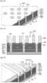
- FIG. 4a illustrates the PROC102 etching of the first semiconductor layer S1 so as to obtain the semiconductor pillars and the qubit layer.
- a first part G of the first semiconductor layer S1 is etched in order to obtain the intermediate circuit illustrated in [ FIG. 4b ].
- said etching PROC102 is advantageously performed anisotropically, ie in a preferential direction, preferentially perpendicular to the free surface of the first semiconductor layer S1.
- Protective pads B made of hard material can be arranged on the surface of the first semiconductor layer S1, to protect part of said layer S1 and make it possible to form a semiconductor pillar PLR under each protective pad B.
- the qubits are preferably arranged in a square lattice having a given pitch.
- a first part of the qubits is intended to form data qubits and a second part of the qubits is intended to form measurement qubits.
- the data and measurement qubits are arranged alternately thus forming a staggered array of data qubits and a staggered array of measurement qubits.
- the staggered arrays of qubits thus have a pitch double compared to the pitch of the square array. Only the The measurement qubits are intended to be arranged plumb with the PLR semiconductor pillars, it is thus advantageous to also arrange the latter in staggered rows.
- the etching PROC102 of the first part G of the first semiconductor layer S1 is also carried out so as to retain a second part QBL of the first semiconductor layer S1, called qubit layer.
- a second part QBL of the first semiconductor layer S1, called qubit layer By keeping, it is meant that the etching PROC102 is for example stopped before the entire thickness of the first semiconductor layer S1 is etched.
- Said etching PROC102 is carried out so that the thickness TQBL of the qubit layer QBL is preferably between 5 nm and 35 nm, preferably between 10 nm and 20 nm, for example equal to 15 nm.
- the plurality of PLR semiconductor pillars thus rely on the qubit layer QBL.
- a first end PLRa of each semiconductor pillar PLR which will be called “base”, rests on the qubit layer QBL.
- a second end PLRb of each semiconductor pillar PLR which will be called “head”, is preferably arranged under a protective pad B.
- the PROC102 etching of the first part G of the first semiconductor layer S1 thus makes it possible to obtain continuity between the PLR pillars and the QBL qubit layer at each PLRa base of the PLR pillars.
- the first semiconductor layer S1 being monocrystalline, the qubit layer QBL and the pillars PLR are therefore made in the same crystal.
- Each PLR pillar may have an HPLR height, measured perpendicular to the qubit layer QBL, greater than 50 nm and preferably greater than or equal to 80 nm.
- Each semiconductor pillar PLR can have one or more flanks F depending on whether the latter is cylindrical or parallelepipedal. For the sake of simplification in the remainder of the description, only the "flank" of a semiconductor pillar will be mentioned to designate the flank or the flanks of said pillar, depending on whether the latter is cylindrical or parallelepipedic.
- the flank F of each PLR pillar is thus arranged plumb with the periphery of each protection pad B.
- the diameter DPLR of each PLR pillar may coincide with the diameter of each protection pad B and is for example between 30 nm and 60 nm, for example equal to 50 nm.
- each PLR pillar may also be less than the diameter of each protective pad B, in particular when the etching implemented is not completely anisotropic.
- the side of each PLR pillar is slightly set back from the plumb of the perimeter of each stud B.
- the PROC method advantageously comprises, before the etching PROC102 of the first semiconductor layer S1, the formation PROC101 of the plurality of protection pads B on the first semiconductor layer S1.
- FIG. 3 schematically shows the formation PROC101 of the plurality of protection pads B on the first semiconductor layer S1.
- the protective pads B are preferably formed by deposition of the hard mask layer, followed by photolithography of a resin mask and anisotropic etching of the pads B through the resin mask.
- the protection pads B can also be formed by photolithography of a resin mask and deposition of a so-called hard mask layer, for example of SiN.
- the protection pads B have an outline that can be circular or rectangular.
- Each protection pad B has a height HB, measured perpendicular to the surface of the first semiconductor layer S1, which can be between 20 nm and 80 nm.
- HB height measured perpendicular to the surface of the first semiconductor layer S1
- the protective pads B are cylindrical, they each have a diameter DB which can be between 30 nm and 60 nm.
- DB diameter of the protective pads B
- the protective pads B are parallelepipedic, they each have a diagonal that can be between 30 nm and 60 nm.
- the term “diameter” will designate both the diameter of the cylindrical studs and the diagonal of the parallelepipedic studs.
- the qubit layer QBL then extends over the insulating layer BOX and more particularly between the plurality of semiconductor pillars PLR and the insulating layer BOX.
- FIG. 5a illustrates a first implementation of the PROC103 oxidation of the side F of each PLR pillar.
- Said PROC103 oxidation is carried out so as to form, at the level of each flank, a first dielectric layer LIN, called “flank dielectric”.
- Each pillar PLR is thus surrounded by a flank dielectric LIN.
- Said PROC103 oxidation is preferably carried out by thermal oxidation, as illustrated by [ FIG. 5b ].
- a flank dielectric LIN completely coats the side of each PLR semiconductor pillar.
- the thickness TLIN of each flank dielectric LIN, measured perpendicular to the free surface of the flank dielectric LIN is preferably between 5 nm and 10 nm.
- PROC103 oxidation can also form a D dielectric layer on the QBL qubit layer. The latter is of less interest since it will be covered by the first separation layer. On the other hand, thermal oxidation forms an oxide of better quality than a deposited oxide. It is therefore advantageous not to remove said dielectric layer D on the qubit layer QBL before depositing the first separation layer.
- Thermal oxidation has the effect of transforming part of the semiconductor material of each PLR pillar into dielectric material.
- the IPL interface between the semiconductor material and the dielectric of each PLR pillar is not plumb APLB with the protection pad B but slightly set back, closer to the center C of each PLR pillar.
- the IPL interface between a PLR pillar and a LIN side dielectric is moved by a distance E1 relative to the plumb APLB of the protection pad B, in the direction of the center C of said PLR pillar.
- the withdrawal of the interface IPL with respect to the plumb APLB makes it possible to protect the semiconductor material of the pillar PLR during the following steps of the PROC method, in particular the steps implementing an anisotropic etching.
- the volume of oxidized material can increase during thermal oxidation, so that the free surface of each LIN flank dielectric can be distant from the plumb APLB of the protective pad B and slightly exposed with respect to said pad B .
- the free surface of a flank dielectric LIN is distant from plumb APLB of protection pad B by a distance E2.
- each flank dielectric LIN a grid at the level of each pillar PLR. It is therefore advantageous, in order to reduce the variability of the manufactured circuits, to check the thickness TLIN of each sidewall dielectric LIN. It is easier to control the thickness of each LIN flank dielectric during their formation, ie during the PROC103 oxidation step, than during anisotropic etching.
- the oxidation step PROC103 comprises a first oxidation sub-step PROC103-1 of the side F of each PLR pillar so as to form, at the level of the side of each PLR pillar, a first sacrificial dielectric layer LINO .
- Each first sacrificial dielectric layer LINO is then removed during a second sub-step PROC103-2, preferably by isotropic etching, to release the free surface of each PLR pillar.
- a third PROC103-3 oxidation sub-step of the newly released surface of each PLR pillar thus makes it possible to form, at the level of the flank of each PLR pillar, a final LIN flank dielectric. Thanks to the etching 103-2 of the first sacrificial layer LINO and the reoxidation 103-3 of the flank of the pillars PLR, the free surface of each flank dielectric LIN is plumb APLB with the protection pad, or slightly set back. Thus, the following steps of the PROC process, which can implement anisotropic etching, do not deteriorate or thin the LIN flank dielectrics. In this way, the variability of behavior of the gates formed with the coupling rows and columns is reduced.
- FIG. 6a illustrates the PROC104 deposition of the first separation layer SEP1, on the qubit layer QBL.
- the first separation layer SEP1 can be made from silicon oxide SiO 2 .
- the first separation layer SEP1 can be deposited, initially, so as to completely cover the PLR pillars as well as the protective pads B, as illustrated by [ FIG. 6b ]. Flattening and anisotropic etching of the first separation layer SEP1 make it possible to control the thickness of said layer SEP1.
- the etching of the flattened first separation layer SEP1 is stopped before reaching the QBL qubit layer.
- the final thickness TSEP1 of the first separation layer SEP1, measured from the qubit layer QBL, is then preferably between 20 nm and 40 nm.
- the PROC104 deposition can be carried out by chemical vapor deposition (or "CVD" in English) and/or plasma-assisted chemical deposition.
- the first separation layer SEP1 covers and surrounds the base PLRa of each pillar PLR.
- FIG. 7a And [ FIG. 7b ] illustrate a structure resulting from the step PROC105 of formation of the plurality of coupling lines CL.
- the coupling lines CL are intended to apply an electrostatic field to each first portion PLR1 of pillar protruding from the first separation layer SEP1, making it possible to allow or block the passage of electrons in the pillar PLR towards the qubit or from the qubit . To do this, they advantageously form, with the flank dielectrics LIN, a gate at the level of each first portion PLR1 of the pillar PLR.
- each coupling line CL In order to improve the coupling of each coupling line CL with a pillar PLR, it is preferable for each coupling line CL to surround a first annular portion LINA1 of the flank dielectric LIN, preferably at the level of the first portion PRL1 of the pillar PLR.
- each coupling line CL is in contact with the flank dielectric LIN surrounding at least one pillar PLR.
- each coupling line CL is formed PROC105 so as to surround a first annular portion LINA1 with at least one flank dielectric LIN projecting from the first separation layer SEP1.
- Each coupling line CL is in contact with at least one flank dielectric LIN.
- Each coupling line CL can also be in contact with a plurality of flank dielectrics LIN.
- a coupling line CL can apply an electrostatic field to a plurality of pillars PLR.
- it allows the indexing of each PLR pillar and therefore of each qubit independently.
- each coupling line CL can contact a plurality of flank dielectrics LIN by extending along a first direction X coinciding with a row of pillars PLR.
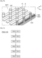
- FIG. 7b illustrates a 3D view of the PLR pillars and the CL coupling lines obtained after their PROC105 formation.
- the pillars are arranged in staggered rows forming rows in the first direction X and columns in a second direction Y.
- the PROC105 formation step can comprise a first conformal PROC105-1 deposition of a first conductive layer M1, for example made of doped polycrystalline silicon or of titanium nitride.
- the first deposit PROC105-1 is preferentially compliant and makes it possible to fully cover the first separation layer SEP1, the flank dielectrics LIN and the protection pads B.
- the first conductive layer M1 can have a thickness TM1 of between 10 nm and 15 nm .
- the PROC105 formation step may include a PROC105-2 deposition of a fifth layer of dielectric D3, illustrated by [ FIG. 7d ], for example silicon oxide, so as to completely cover the assembly.
- the PROC105 formation step may also include PROC105-3 etching of the fifth dielectric layer D3, as illustrated by the [ FIG. 7th] and [FIG. 7f ], made anisotropically and selectively with respect to the first conductive layer M1.
- the first PROC105-3 etching exposes a plurality of CAP portions of the first conductive layer M1, called "caps". Each cap CAP covers a protective pad B and an upper portion of a pillar PLR.
- the PROC105-3 etching of the fifth dielectric layer D3 is stopped so as to leave a residual thickness TD3 of 10 nm to 15 nm, at the base of each cap CAP.
- the PROC105 formation step may also include a PROC105-4 etching of the first conductive layer M1 and of the fifth dielectric layer D3, as illustrated by the [ FIG. 7g] and [FIG. 7am ], so as to remove the plurality of caps CAP as well as the residual thickness TD3 of the fifth dielectric layer D3.
- the remaining first conductive layer M1 then extends over the first separation layer SEP1 and surrounds a first annular portion LINA1 of each flank dielectric LIN.
- the PROC105-4 etching of the first conductive layer M1 can be carried out in one go, for example by non-selective and isotropic etching, making it possible to remove at the same time the plurality of caps CAP and the residual thickness TD3 of the fifth layer dielectric D3.
- the residual thickness TD3 of the fifth dielectric layer D3 is then advantageously chosen so that it is completely withdrawn when the CAPs are removed.
- PROC105-4 etching can also be performed in two sub-steps.
- a first sub-step comprising a selective etching of the first conductive layer M1 with respect to the residual thickness TD3 of the fifth dielectric layer D3 so as to remove the caps CAP.
- a second sub-step comprising an anisotropic etching of the residual thickness TD3 of the fifth dielectric layer D3 so as to remove the fifth dielectric layer D3.
- the second sub-step is stopped before substantially etching the first conductive layer M1.
- the formation step PROC105 may comprise the etching PROC105-6 of the first conductive layer M1 through this resin mask so as to obtain the coupling lines CL.
- the PROC105 formation step may for example comprise, before said PROC105-6 etching, a PROC105-5 photolithography of a resin mask on the first conductive layer M1, followed by the PROC105-6 etching of the first conductive layer M1 at through the resin mask so as to obtain the coupling lines CL.
- the coupling lines are preferentially substantially parallel to each other and preferentially extend along the first direction X. By substantially parallel is meant within ⁇ 30°, preferentially within ⁇ 20°, or even within ⁇ 10°.
- the caps CAP are removed, for example by selective etching.
- the residual thickness TD3 of the fifth dielectric layer D3 is then used to form a mask during the aforementioned photolithography sub-step PROC105-5 and thus allow the etching PROC105-6 of the coupling lines CL through said mask.
- the fifth dielectric layer D3 is removed, for example by selective etching, after the coupling lines CL have been obtained.
- FIG. 8 schematically presents the PROC106 deposition step of the second separation layer SEP2.
- the second separation layer SEP2 is deposited so as to cover the plurality of coupling lines CL, thus ensuring their electrical insulation.
- the second separation layer SEP2 can also be deposited so as to cover the first separation layer SEP1.
- the PROC106 deposition of the second separation layer SEP2 is advantageously carried out in the same way as the deposition of the first separation layer SEP1, as illustrated by the [ FIG. 6a] and [FIG. 6b ].
- the second separation layer SEP2 can for example be made from silicon oxide SiO 2 .
- the thickness TSEP2 of the second separation layer SEP2 is preferably between 20 nm and 40 nm. Said thickness TSEP2 is measured from the first separation layer SEP1 on which the coupling lines CL rest.
- the thickness TSEP2 of the second separation layer SEP2 is preferably chosen so that at least a second portion PLR2 of each pillar PLR protrudes from the second separation layer SEP2.
- FIG. 9a illustrates the step PROC107 of forming the plurality of DC coupling columns.
- the coupling columns CC advantageously form, with the flank dielectrics LIN, a grid at the level of each pillar PLR.
- the coupling rows and columns CL, CC are thus intended to apply an electrostatic field to the first and second portions PLR1, PLR2 of the same pillar PLR, making it possible to authorize or block the passage of electrons in said pillar PLR.
- the coupling rows and columns CL, CC are arranged so that applying an electric potential to one of the rows CL and one of the columns CC makes it possible to authorize or block the passage of electrons from a single pillar PLR among the plurality of PLR pillars.
- the coupling rows and columns CL, CC thus allow the individual indexing of the qubits to, for example, initialize or measure their state.
- each coupling column CC is in contact with at least one flank dielectric LIN.
- each coupling column CC is formed PROC107 so as to surround a second annular portion LINA2 with at least one flank dielectric LIN, protruding from the second separation layer SEP2.
- the coupling columns CC advantageously extend over the second separation layer SEP2.
- the latter covering the coupling lines CL, makes it possible to provide electrical insulation between the lines and the coupling columns CL, CC.
- a capacitive coupling may remain between the rows and the coupling columns CL, CC.
- substantially right angle is meant straight to within ⁇ 30°, preferably to within ⁇ 20°, or even to within ⁇ 10°.
- the CC coupling columns preferentially extend parallel to each other and along the second Y direction. Thus, they can contact the LIN flank dielectrics of a plurality of PLR pillars aligned along the second Y direction and reduce the capacitive coupling with the coupling lines CL.
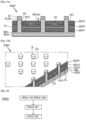
- FIG. 9b illustrates a 3D view of the PLR pillars, the CL coupling lines and the CC coupling columns obtained at the end of the PROC107 formation step of the CC columns.
- the coupling columns CC are then preferentially oriented perpendicular to the coupling lines CL. It is however possible for the coupling columns CC to form another angle with the coupling lines CL, for example equal to 45°. In which case, the second DC conductive electrodes are called "coupling diagonals".
- the PROC107 formation step of the CC coupling columns is preferentially similar to the PROC105 formation step of the CL coupling lines as illustrated by the [ FIG. 7a] to [FIG. 7am ].
- THE [ FIG. 10a] and [FIG. 10b ] illustrate the PROC108 deposition step of the third separation layer SEP3.
- Said third separation layer SEP3 rests on the plurality of coupling columns CC and encapsulates said plurality of columns CC.
- the PROC108 deposition of the third separation layer SEP3 can be carried out in the same way as the PROC105 deposition of the first separation layer SEP1, as illustrated by the [ FIG. 6a] and [FIG. 6b ] and/or the PROC107 deposit of the second separation layer SEP2.
- the third separation layer SEP3 can also be made from silicon oxide SiO 2 .
- the third separation layer SEP3 coats the coupling columns CC and can also cover the second separation layer SEP2.
- the third separation layer SEP3 has a thickness TSEP3 measured from the second separation layer SEP2 on which the coupling columns CC rest.
- the thickness TSEP3 of the third separation layer SEP3 is configured so that a third portion PLR3 of each pillar PLR protrudes from said third separation layer SEP3.
- the third annular portion LINA3 then extends over the entire height HLPR3 of the third PLR pillar portion PLR3, that is to say from the free surface FSEP3 of the third layer SEP3 to the top of each pillar PLR, thus flush with the protective pads B placed on each PLR pillar.
- the thickness TSEP3 of the third separation layer SEP3 and/or the height HPLR of each pillar PLR is chosen so that the height HPLR3 of the third portion PLR3 is between 5 nm and 20 nm inclusive, for example 10 nm.
- the thickness TSEP3 of the third separation layer SEP3 can be between 20 nm and 40 nm.
- the third separation layer SEP3 In order to adjust the thickness TSEP3 of the third separation layer SEP3, it can be, initially, deposited so as to exceed the top of the protection pads B. Secondly, it can be flattened up to flush with the top of the protective pads B. Finally, the third separation layer SEP3 can be etched anisotropically in order to expose the protective pads B and the third annular portion LINA3 of each flank dielectric LIN.
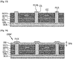
- FIG. 11a and [FIG. 11b ] illustrate the etching PROC109 of the third annular portions LINA3 of each flank dielectric LIN so as to expose the third portion PLR3 of each pillar PLR.
- the third pillar portion PLR3 thus exposes a contact surface CS, called "contact surface".
- the contact surface CS can be used to electrically connect the PLR pillar to a conductive electrode so as to allow the passage of electrons to or from the qubit layer QBL.
- the CS contact surface can also be connected to a device for reading the quantum state of a qubit, making it possible to read the state of the qubit located directly above said PLR pillar.
- the PROC109 etching of the third annular portions LINA3 of each flank dielectric LIN is preferably carried out in such a way as to remove them completely.
- said PROC109 etching can be carried out selectively, at least with respect to the protection pads B.
- the flank dielectrics LIN are composed of SiO 2
- the PROC109 etching can be carried out by means of dilute hydrofluoric acid HF.
- the PROC process thus makes it possible to manufacture a quantum electronic circuit DISP comprising a qubit layer QBL and a plurality of PLR pillars made from a single and same crystal and which can be integrated into a quantum electronic system.
- Said circuit DISP is remarkable in that the qubit layer QBL and each semiconductor pillar PLR belong to the same monocrystalline semiconductor material and thus have crystalline continuity.
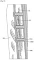
- FIG. 13 illustrates the PROC201 removal of each protective pad B, so as to release the PLRb head from each PLR pillar.
- the removal of the sacrificial pads B can be carried out by selective etching with respect to each pillar PLR and/or the third separation layer.
- the etching can for example be carried out by means of phosphoric acid H 3 PO 4 .
- FIG. 14 illustrates the PROC202 deposit of the INI initialization layer so that it is in contact with each PLR pillar. It covers for example at least the heads PLRb and the contact surfaces CS of each pillar PLR.
- the initialization layer INI is in electrical contact with each PLR pillar and makes it possible to function as an electron reservoir in order to initialize each qubit directly above the connected PLR pillars.
- the initialization layer INI is for example made from heavily doped polycrystalline silicon. Its thickness TINI is preferably between 20 nm and 40 nm.
- the PROC202 deposition of the INI initialization layer may comprise the epitaxy deposition of phosphorus-doped silicon Si:P or silicon and boron-doped germanium SiGe:B.
- the epitaxy is preferably carried out selectively in order to be initiated from the exposed end of each pillar PLR, that is to say their head PLRb and their contact surface CS.
- the deposition PROC202 of the initialization layer INI can also comprise a step of siliciding said initialization layer INI, after the actual deposition of said layer INI.
- the silicidation is for example carried out by means of platinum nitride NiPt.La [ FIG. 15 ] schematically presents the quantum electronic device DISP capable of being obtained at the end of the manufacturing process according to the second mode of implementation.
- the first, second and third separation layers SPE1, SEP2, SEP3 are masked in order to present, with respect to each PLR pillar and to the qubit layer QBL, the superposition of the coupling lines CL, the coupling columns CC and the layer INI initialization.
- the embodiment of the DISP circuit of the [ FIG. 15 ] thus differs from the embodiment of the [ FIG. 11a] and [FIG. 11b ] in that the circuit DISP also comprises an initialization layer INI contact with each semiconductor pillar PLR.
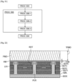
- FIG. 16 ] schematically presents a third embodiment of the manufacturing process PROC, making it possible to obtain the quantum electronic DISP circuit according to a third embodiment.
- the method PROC according to the third embodiment makes it possible to obtain a quantum electronic circuit DISP comprising a read layer as well as a single electron transistor at the top of each PLR pillar.
- each RDT read line formed is preferably at least in contact with a PLR pillar. In order to obtain good electrical contact between the read lines and the PLR pillars, it is advantageous for each RDT read line to be in contact with the contact surface CS of a PLR pillar.
- the read lines RDT extend along the first direction X and connect the contact surface CS of a plurality of pillars PLR.
- Each RDT read line can also be in contact with the flank K of a protective pad B.
- the RDT read lines extend over the third separation layer SEP3 and cover each protective pad B.
- the latter are advantageously oriented perpendicular to the DC coupling columns.
- the PROC301 formation of the RDT read lines may initially comprise the deposition of a second conductive layer M2 on the contact surface CS of each pillar PLR, on each protective pad B and on the third separation layer SEP3, such as as illustrated by the [ FIG. 17c] and [FIG. 17d ].
- the second conductive layer M2 has a thickness TM2 which can be between 10 nm and 15 nm.
- the second conductive layer M2 can be made from doped polysilicon. Its deposition can be preceded by an epitaxy of silicon doped with phosphorus Si:P or of silicon and germanium doped with boron SiGe:B. In this way, the interface between the contact surface CS of each pillar and the second conductive layer M2 is improved.
- the PROC301 formation of the RDT read lines can also comprise the structuring of the second conductive layer M2 so as to obtain each RDT read line as illustrated by the [ FIG. 17a] and [FIG. 17b ].
- the structuring of the second conductive layer M2 can be carried out by photolithography of a resin mask through which the second conductive layer M2 is etched.
- the structuring is preferably carried out so as to form RDT read lines substantially parallel to each other.
- substantially parallel is meant parallel to within ⁇ 30°, preferably within ⁇ 20°, or even within ⁇ 10°. It is also made so as to arrange two RDT read lines on either side of a pillar PLR, each of the lines being at least in contact with the contact surface CS of said pillar PLR.
- the RDT read lines illustrated by the [ FIG. 17a] and [FIG. 17b ] also include a plurality of transverse portions RDTT completely covering the protective pads B and the contact surface CS of the PLR pillars.
- the transverse portions RDTT appear when the photolithographed resin mask comprises portions above each PLR pillar, protecting the latter during etching and avoiding removing the second conductive layer M2 from the flanks K of the protective pads B and from the contact surfaces CS.
- the structuring of the second conductive layer M2 can also be carried out in a self-aligned manner, without requiring transverse portions RDTT.
- the etching of the second conductive layer M2 is for example performed anisotropically through a photolithographed resin mask not comprising portions above each pillar PLR.
- the topology of each pillar PLR has the effect of forming second conductive layer spacers M2 around each pillar PLR.
- FIG. 18a ] and [ FIG. 18b ] illustrate the PROC302 deposition steps of the fourth separation layer SEP4 and PROC303 flattening of the fourth separation layer SEP4.
- the PROC302 deposition of the fourth separation layer SEP4 is carried out in such a way as to cover the entire structure, in particular the RDT reading lines and preferably the third separation layer SEP3 and the protective pads B when these are not covered by RTD read lines.
- the fourth separation layer SEP4 can be made from silicon oxide.
- the fourth separation layer SEP4 is then flattened PROC303 until the top of the protective pads B is freed. During this step PROC303, part of each RDT read line can be removed, in particular when the latter cover the protective pads B By doing so, each protective pad B emerges from the surface of the fourth separation layer SEP4.
- FIG. 19a] and [FIG. 19b ] illustrate the selective PROC304 etching of the protection pads B with respect to the fourth separation layer SEP4 and with respect to the RDT read lines.
- PROC304 etching can be performed isotropically. It is preferably stopped on the top of each PLR pillar, revealing the semiconductor material of each PLR pillar.
- the PROC304 etching of the protection pads B thus makes it possible to form a plurality of cavities CAV plumb with each pillar PLR. Each CAV cavity is preferably surrounded by a read line RDT.
- Each cavity CAV is intended to accommodate a charging gate CHAR making it possible to form, with a pillar PLR and a read line RDT, a single-electron transistor.
- THE [ FIG. 19a] and [FIG. 19b ] illustrate a first step in the PROC305 formation of the CHAR loading gate, in each CAV cavity. Firstly, the walls of each CAV cavity, and preferably the visible parts of the RDT read lines, are oxidized so as to form a seventh dielectric layer OX, called “gate oxide”.
- the gate oxide OX is preferably formed by thermal oxidation and advantageously has a thickness of between 2 nm and 5 nm.
- the PROC305 formation of the CHAR loading grid also includes the filling of each CAV cavity, as illustrated by the [ FIG. 20a] and [FIG. 20b ], with a conductive material such as a metal or a set of metal layers.
- the filling of each CAV cavity comprises for example a conformal deposition of a first metallic layer, for example of titanium Ti, so as to cover the gate oxide OX at the bottom of each CAV cavity.
- the filling of the CAV cavities can also comprise the conformal deposition of a layer of silicide, for example titanium nitride TiN, so as to cover the first metallic layer.
- the filling may comprise the deposition of a second metallic layer, for example of tungsten W, covering the layer of silicide and completely filling each cavity CAV.
- CHAR loading gates can be structured to connect a plurality of single electron transistors. They are advantageously substantially parallel to each other and oriented along one of the first or second directions X, Y. In this way, the CHAR loading gates can control a plurality of PLR pillars. However, in order to reduce the capacitive coupling between the read lines RDT and the charging gates CHAR, the latter are advantageously oriented perpendicular to the read lines RDT.
- the method PROC can comprise a step of forming PROC306 of corridors CLR, each CLR lane being preferentially aligned with a plurality of PLR pillars.
- the charging gates CHAR are then preferentially formed in each lane CLR.
- the CHAR loading gates are thus isolated in pairs.
- the CLR corridors are separated two by two by a PAR wall.
- the PROC306 formation step of the CLR corridors schematized by the [ FIG. 21 ]. It includes a first sub-step PROC306-1, illustrated by [ FIG.22 ], comprising the deposition of a hard mask HM covering the fourth separation layer SEP4, the read lines RDT and the protection pads B.
- the hard mask layer can be made from silicon nitride SiN or silicon nitride titanium TiN. It preferably has a THM thickness of between 10 nm and 30 nm.
- the formation step PROC306 of the CLR corridors includes a second sub-step PROC306-2, also illustrated by the [ FIG. 22 ], comprising the deposition of a PMD encapsulation layer covering the hard mask HM.
- the PMD encapsulation layer is preferably made from silicon oxide SiO 2 and may have a TPMD thickness greater than 80 nm.
- the PMD encapsulation and HM hard mask layers are then etched during a third sub-step PROC306-3, illustrated by the [ FIG. 23a] and [FIG. 23b ], so as to form trenches in the aforementioned materials, forming the CLR corridors.
- the PROC306-3 etching is preferably carried out through a resin mask obtained by a photolithography step.
- the etching of the PMD encapsulation and HM hard mask layers stops at the level of the top of the protection pads B.
- the PAR walls separating the corridors then comprise advantageously a portion of hard mask HM and a portion of encapsulation layer PMD.
- the PROC304 etching step of the protection pads B is advantageously carried out when the PAR walls separating the corridors are already in place.
- the PROC306 training step of the CHAR loading gates illustrated by the [ FIG. 20a] and [FIG. 20b ] makes it possible to obtain structured CHAR grids that are isolated from each other.
- the PROC306 formation of the CHAR charging gates can then include the conformal deposition of the metallic layer in each CAV cavity and in each CLR lane. The same is true for the conformal deposition of the silicide layer. Filling each CAV cavity can also fill each CLR lane. At the end of the PROC306 formation step of the CHAR charging gates, flattening can be carried out so as to guarantee the absence of a short-circuit between the charging gates.
- FIG. 24 schematically presents the quantum electronic DISP circuit capable of being obtained at the end of the manufacturing process according to the third mode of implementation.
- the first, second, third and fourth separation layers SPE1, SEP2, SEP3, SEP4 are masked in order to present, with respect to each PLR pillar and to the qubit layer QBL, the superposition of the coupling lines CL, the coupling columns CC , RDT readlines and CHAR loading grids.
- FIG. 25 schematically presents the DISP circuit obtained during a development of the PROC method.
- a plurality of control grid GC can be added to the previously obtained circuit so as to control and manipulate the state of each qubit.
- the DISP circuit is returned.
- the circuit DISP is made from an SOI-type substrate, ie comprising an insulating layer BOX buried under the qubit layer QBL, then it is etched until it reaches the insulating layer BOX.
- a plurality of control gates GC made of a conductive material, is formed on the insulating layer BOX.
- the control gates GC are preferably substantially parallel to each other and are arranged between each pillar PLR.
- the BOX insulating layer can be thinned. It can also be completely removed and so as to deposit a new oxide layer, for example thinner than the insulating layer BOX, on the qubit layer QBL. The plurality of control gates GC is then formed on the new oxide layer.
Landscapes
- Engineering & Computer Science (AREA)
- Power Engineering (AREA)
- Microelectronics & Electronic Packaging (AREA)
- Physics & Mathematics (AREA)
- General Physics & Mathematics (AREA)
- Condensed Matter Physics & Semiconductors (AREA)
- Computer Hardware Design (AREA)
- Ceramic Engineering (AREA)
- Theoretical Computer Science (AREA)
- Nanotechnology (AREA)
- Chemical & Material Sciences (AREA)
- Computational Mathematics (AREA)
- Computing Systems (AREA)
- Artificial Intelligence (AREA)
- Software Systems (AREA)
- Data Mining & Analysis (AREA)
- Evolutionary Computation (AREA)
- Mathematical Analysis (AREA)
- Mathematical Optimization (AREA)
- Pure & Applied Mathematics (AREA)
- Mathematical Physics (AREA)
- General Engineering & Computer Science (AREA)
- Manufacturing & Machinery (AREA)
- Crystallography & Structural Chemistry (AREA)
- Materials Engineering (AREA)
- Drying Of Semiconductors (AREA)
- Semiconductor Integrated Circuits (AREA)
- Semiconductor Memories (AREA)
Abstract
L'invention concerne un procédé de fabrication d' un circuit électronique quantique comprenant une couche semi-conductrice destinée à recevoir des qubits dans des îlots quantiques. La couche qubits peut recevoir les qubits pendant leur stockage et leur manipulation.Un aspect de l'invention concerne un procédé de fabrication d'un circuit (DISP) électronique quantique comprenant les étapes suivantes :- graver une couche semiconductrice de manière à obtenir :- une pluralité de piliers (PLR) chaque pilier semi-conducteur présentant une première extrémité, dite "base"; et- une couche qubits (QBL) à la base de chaque pilier semiconducteur ;;- oxyder le flanc de chaque pilier (PLR) ;- former des lignes de couplage (CL) et des colonnes de couplage (CC) ; et- déposer des couches de séparation (SEP1, SEP2, SEP3) en laissant dépasser une surface de contact (CS) de chaque pilier (PLR).The invention relates to a method for manufacturing a quantum electronic circuit comprising a semiconductor layer intended to receive qubits in quantum islands. The qubit layer can receive the qubits during their storage and handling. One aspect of the invention relates to a method for manufacturing a quantum electronic circuit (DISP) comprising the following steps:- etching a semiconductor layer so as to obtain:- a plurality of pillars (PLR), each semiconductor pillar having a first end, called the "base"; and- a qubit layer (QBL) at the base of each semiconductor pillar;;- oxidizing the flank of each pillar (PLR);- forming coupling lines (CL) and coupling columns (CC); and- depositing separation layers (SEP1, SEP2, SEP3) leaving a contact surface (CS) of each pillar (PLR) protruding.
Description
Le domaine technique de l'invention est celui de l'électronique quantique et plus particulièrement la fabrication d'un circuit électronique quantique.The technical field of the invention is that of quantum electronics and more particularly the manufacture of a quantum electronic circuit.
La manipulation d'états quantiques, également appelés "qubits" pour "quantum bits" en anglais, offre de nouvelles possibilités dans la manipulation d'information. Les circuits électroniques quantiques à même de permettre la manipulation de qubits, comprennent des îlots, également appelés boîtes quantiques. Les boîtes quantiques sont capables stocker des qubits le temps de leur manipulation et de leur mesure.The manipulation of quantum states, also called "qubits" for "quantum bits" in English, offers new possibilities in the manipulation of information. Quantum electronic circuits capable of manipulating qubits include islands, also called quantum dots. Quantum dots are able to store qubits while they are being manipulated and measured.
L'intégration de boîtes quantiques sous forme de circuits électroniques quantiques doit satisfaire plusieurs exigences. D'une part offrir une haute densité de boîtes quantiques afin d'offrir une capacité calculatoire conséquente. D'autre part, les procédés de fabrication desdits circuits électroniques quantiques doivent permettre d'atteindre une cadence de production industrielle tout en assurant une faible variabilité des circuits. En effet, le stockage et la manipulation des qubits au sein de boîtes quantiques sont fortement tributaires des couplages entre les différents composants formant les circuits électroniques quantiques.The integration of quantum dots in the form of quantum electronic circuits must satisfy several requirements. On the one hand, to offer a high density of quantum dots in order to offer a substantial computing capacity. On the other hand, the manufacturing methods of said quantum electronic circuits must make it possible to achieve an industrial production rate while ensuring low variability of the circuits. Indeed, the storage and manipulation of qubits within quantum dots are highly dependent on the couplings between the different components forming the quantum electronic circuits.
Les circuits électroniques quantiques doivent offrir la possibilité de coupler plusieurs qubits entre eux pour permettre d'effectuer un calcul à partir d'un ensemble de qubits. Dans certains cas, l'opération de couplage s'effectue en contrôlant un couplage tunnel entre des boites quantiques contenant les qubits. En revanche, le contrôle des couplages tunnels impose une architecture des boites quantiques interconnectées sous forme de matrices denses. De plus, les boîtes quantiques doivent également pouvoir être couplées à des réservoirs de porteurs de charge et des détecteurs de charge. Afin de permettre la densification des boîtes quantiques, il est proposé d'intégrer et connecter les réservoirs de porteurs de charges et les détecteurs de charges dans des plans différents du plan comprenant les boîtes quantiques. On parle dans ce cas de circuits à architecture non-planaire, dite également "3D" pour "à 3 dimensions".Quantum electronic circuits must offer the possibility of coupling several qubits together to allow a calculation to be performed from a set of qubits. In some cases, the coupling operation is performed by controlling tunnel coupling between quantum dots containing the qubits. On the other hand, the control of tunnel couplings imposes an architecture of interconnected quantum dots in the form of dense matrices. In addition, quantum dots must also be able to be coupled to charge carrier reservoirs and charge detectors. In order to allow the densification of the quantum boxes, it is proposed to integrate and connect the reservoirs of charge carriers and the charge detectors in planes different from the plane comprising the boxes. quantum. In this case, we speak of circuits with a non-planar architecture, also called "3D" for "3 dimensions".
Deux types de circuits à architecture 3D émergent aujourd'hui. Les circuits dits à contrôle individuel des qubits d'une part, également appelé "fully controlled" en anglais, et les circuits dits à contrôle parallèle des qubits d'autre part, également appelé "crossbar network". Si les circuits à contrôle individuel facilitent la manipulation des qubits, ils présentent en revanche une architecture électrique complexe, avec une forte densité de vias et d'interconnexions. Les circuits à contrôle parallèle offrent quant à eux une architecture plus simple, notamment grâce à la réduction de la densité de vias et d'interconnexions.Two types of circuits with 3D architecture emerge today. The so-called individual qubit control circuits on the one hand, also called "fully controlled" in English, and the so-called parallel qubit control circuits on the other hand, also called "crossbar network". If the individually controlled circuits facilitate the manipulation of qubits, they present on the other hand a complex electrical architecture, with a high density of vias and interconnections. Parallel control circuits offer a simpler architecture, in particular thanks to the reduction in the density of vias and interconnections.
La demande de brevet
Le procédé divulgué comprend également la formation de piliers traversant de part et d'autre ladite couche de matériau diélectrique et les réseaux d'électrodes jusqu'à atteindre les boîtes quantiques. L'étape de formation des piliers comprend une gravure de la couche diélectrique et des réseaux d'électrodes enrobés de manière à former des cavités évidées atteignant la surface des boîtes quantiques. Une reprise de contact au niveau des boîtes quantiques est réalisée par épitaxie d'un matériau semiconducteur dans les cavités évidées. L'étape de formation des piliers comprend également, avant la reprise de contact, la formation d'une couche d'oxyde sur les parois latérales des cavités évidées afin d'isoler les piliers des réseaux d'électrodes enrobés. Les piliers semiconducteurs ainsi formés, en contact avec les boîtes quantiques, permettent l'initialisation des qubits ainsi que leur mesure.The method disclosed also comprises the formation of pillars passing through said layer of dielectric material and the arrays of electrodes on either side until they reach the quantum dots. The step of forming the pillars includes an etching of the dielectric layer and arrays of coated electrodes so as to form recessed cavities reaching the surface of the quantum dots. A resumption of contact at the level of the quantum dots is carried out by epitaxy of a semiconductor material in the hollow cavities. The step of forming the pillars also comprises, before the resumption of contact, the formation of an oxide layer on the side walls of the recessed cavities in order to isolate the pillars from the networks of coated electrodes. The semiconductor pillars thus formed, in contact with the quantum boxes, allow the initialization of the qubits as well as their measurement.
En revanche, ce procédé pose quelques problèmes. Dans un premier temps, la formation des boîtes quantiques à lieu en face avant d'un substrat de silicium sur isolant (SOI en anglais) tandis que la formation des réseaux d'électrodes et la reprise de contact des piliers sont réalisées en face arrière dudit substrat. Le procédé impose donc une étape de collage et de retournement du substrat et une libération de la face arrière des boîtes quantiques. Les étapes de collage/retournement peuvent être difficiles à réaliser et peuvent occasionner des défauts au niveau de l'interface de collage, tels qu'un désordre électrostatique. De plus, les variations d'alignements des piliers par rapport aux boîtes quantiques peuvent modifier le couplage entre lesdits piliers et boîtes quantiques.However, this process poses some problems. Initially, the formation of the quantum dots takes place on the front face of a silicon-on-insulator (SOI) substrate while the formation of the electrode networks and the resumption of contact of the pillars are carried out on the rear face of said substrate. The method therefore imposes a step of bonding and turning over the substrate and a release of the back side of quantum dots. The bonding/turning steps can be difficult to perform and can cause defects at the bonding interface, such as electrostatic disorder. In addition, the alignment variations of the pillars with respect to the quantum dots can modify the coupling between said pillars and quantum dots.
Dans un second temps, la formation de la couche d'oxyde dans les cavités évidés est dans un premier temps réalisée au niveau des bords latéraux et du fond de la cavité. Le fond de la cavité est ensuite libéré par gravure anisotrope pour mettre à nu la surface des boîtes quantiques et permettre l'épitaxie des piliers à partir des boîtes quantiques. Le dépôt d'oxyde suivie d'une gravure anisotrope peut rendre l'interface entre les boîtes quantiques et le pilier défectueuse.In a second step, the formation of the oxide layer in the hollowed out cavities is initially carried out at the level of the side edges and of the bottom of the cavity. The bottom of the cavity is then released by anisotropic etching to expose the surface of the quantum dots and allow the epitaxy of the pillars from the quantum dots. Oxide deposition followed by anisotropic etching can make the interface between the quantum dots and the pillar defective.
Le procédé divulgué ne permet donc pas de réduire la variabilité des circuits produits.The method disclosed therefore does not make it possible to reduce the variability of the circuits produced.
L'invention offre une solution au problème évoqué, en permettant de réaliser un circuit électronique quantique sans interface entre les piliers semiconducteurs et une couche semiconductrice destinée à recevoir les boîtes quantiques.The invention offers a solution to the problem mentioned, by making it possible to produce a quantum electronic circuit without an interface between the semiconductor pillars and a semiconductor layer intended to receive the quantum dots.
Pour cela, l'invention concerne un procédé de fabrication d'un circuit électronique quantique, le procédé étant mis en œuvre à partir d'un substrat comportant sur l'une de ses surfaces une première couche semiconductrice monocristalline et comprenant les étapes suivantes :
- graver la première couche semiconductrice de manière à :
- obtenir une pluralité de piliers semiconducteurs, chaque pilier semiconducteur présentant une première extrémité, dite "base" ; et
- conserver une partie de la première couche semiconductrice dite "couche qubits", à la base de chaque pilier semiconducteur ;
- oxyder le flanc de chaque pilier semiconducteur de manière à former une pluralité de premières couches diélectriques, dites "diélectriques de flanc" ;
- déposer une deuxième couche diélectrique, dite "première couche de séparation", sur la couche qubits ;
- former une pluralité de premières électrodes conductrices sensiblement parallèles entre elles, dites "lignes de couplage", sur la première couche de séparation, chaque ligne de couplage étant en contact avec le diélectrique de flanc d'au moins un pilier semiconducteur ;
- déposer une troisième couche diélectrique, dite "deuxième couche de séparation", sur la pluralité de lignes de couplage ;
- former une pluralité de deuxièmes électrodes conductrices sensiblement parallèles entre elles, dites "colonnes de couplage", sur la deuxième couche de séparation, chaque colonne de couplage étant en contact avec le diélectrique de flanc d'au moins un pilier semiconducteur ;
- déposer une quatrième couche diélectrique, dite "troisième couche de séparation", sur la pluralité de colonnes de sorte qu'une portion de chaque diélectrique de flanc dépasse de la troisième couche de séparation ; et
- graver chaque portion des diélectriques de flanc dépassant de la troisième couche de séparation afin d'exposer une surface de chaque pilier semiconducteur, dite "surface de contact".
- etching the first semiconductor layer so as to:
- obtaining a plurality of semiconductor pillars, each semiconductor pillar having a first end, called the "base"; And
- keep a part of the first semiconductor layer called "qubit layer", at the base of each semiconductor pillar;
- oxidizing the flank of each semiconductor pillar so as to form a plurality of first dielectric layers, called “flank dielectrics”;
- depositing a second dielectric layer, called "first separation layer", on the qubit layer;
- forming a plurality of first conductive electrodes substantially parallel to one another, called "coupling lines", on the first separation layer, each coupling line being in contact with the flank dielectric of at least one semiconductor pillar;
- depositing a third dielectric layer, called "second separation layer", on the plurality of coupling lines;
- forming a plurality of second conductive electrodes substantially parallel to one another, called "coupling columns", on the second separation layer, each coupling column being in contact with the flank dielectric of at least one semiconductor pillar;
- depositing a fourth dielectric layer, called "third separation layer", on the plurality of columns so that a portion of each flank dielectric protrudes from the third separation layer; And
- etching each portion of the flank dielectrics protruding from the third separation layer in order to expose a surface of each semiconductor pillar, called the “contact surface”.
Le procédé permet ainsi de fabriquer un circuit électronique quantique comprenant une couche qubits dans laquelle peuvent être formés les boîtes quantiques destinées à recevoir les qubits. Le procédé permet de former des piliers semiconducteurs présentant une continuité cristalline avec la couche qubits. Ainsi, la variabilité des circuits produits est réduite.The method thus makes it possible to manufacture a quantum electronic circuit comprising a qubit layer in which the quantum boxes intended to receive the qubits can be formed. The method makes it possible to form semiconductor pillars having crystalline continuity with the qubit layer. Thus, the variability of the circuits produced is reduced.
Outre les caractéristiques qui viennent d'être évoquées dans le paragraphe précédent, le procédé selon l'invention peut présenter une ou plusieurs caractéristiques complémentaires parmi les suivantes, considérées individuellement ou selon toutes les combinaisons techniquement possibles :
- l'épaisseur de la couche qubits est comprise entre 5 nm et 35 nm ;
- les lignes de couplage croisent les colonnes de couplages préférentiellement selon un angle sensiblement droit ;
- la première couche semiconductrice est en silicium et de préférence enrichi par un isotope, par exemple le silicium 28 ;
- la première couche semiconductrice comprend une couche semiconductrice monocristalline en face avant et une couche semiconductrice monocristalline épitaxiée, la couche semiconductrice monocristalline épitaxiée étant obtenue au moyen d'une épitaxie pleine plaque à partir de la couche semiconductrice monocristalline en face avant.
- l'étape d'oxydation permettant de former le diélectrique de flanc pour chaque pilier semiconducteur comprend les sous-étapes suivantes : oxyder la surface libre de chaque pilier semiconducteur de sorte à former, au niveau du flanc de chaque pilier semiconducteur, une couche diélectrique sacrificielle ; retirer la couche diélectrique sacrificielle ; et oxyder la surface libre de chaque pilier semiconducteur de sorte à former, au niveau du flanc de chaque pilier semiconducteur, le diélectrique de flanc ;
- chaque diélectrique de flanc est obtenu par oxydation thermique du flanc de chaque pilier semiconducteur ;
- la formation de la pluralité de lignes de couplage comprend : déposer de manière conforme d'une première couche conductrice recouvrant intégralement la première couche de séparation et chaque pilier semiconducteur; déposer une cinquième couche de diélectrique de manière à recouvrir complètement la première couche conductrice ; graver la cinquième couche de diélectrique de manière à mettre à nu une pluralité de portions de la première couche conductrice, dites "capuchons", et conserver une épaisseur résiduelle de la cinquième couche de diélectrique, chaque capuchon recouvrant une portion supérieure de chaque pilier semiconducteur ; graver la première couche conductrice et la cinquième couche diélectrique de manière à retirer chaque capuchon et l'épaisseur résiduelle de la cinquième couche diélectrique ; et graver la première couche conductrice de manière à obtenir les lignes de couplage ;
- le procédé comprend, avant la gravure de la première couche semiconductrice, la formation d'une pluralité de plots de protection sur la première couche semiconductrice, la gravure de la première couche semiconductrice comprenant une gravure anisotrope d'une première partie de la première couche semiconductrice de manière à obtenir un pilier semiconducteur sous chaque plot sacrificiel ;
- le procédé comprend, après la gravure de chaque portion des diélectriques de flancs, les étapes supplémentaires suivantes : retirer le plot de protection de chaque pilier semiconducteur de manière à exposer la deuxième extrémité dudit pilier semiconducteur ; et déposer une couche conductrice dopée, dite "couche d'initialisation", recouvrant au moins la deuxième extrémité et la surface de contact de chaque pilier semiconducteur ;
- la couche d'initialisation est en silicium polycristallin fortement dopé ;
- le procédé comprend, après le dépôt de la couche d'initialisation, la formation de contacts conducteurs au niveau de chaque ligne de couplage, de chaque colonne de couplage et de la couche d'initialisation ;
- le procédé comprend, après la gravure de chaque portion des diélectriques de flancs, les étapes supplémentaires suivantes : former une pluralité de troisièmes électrodes conductrices dopées, dites "lignes de lecture", chaque ligne de lecture étant en contact avec au moins un pilier semiconducteur ; déposer une sixième couche diélectrique, dite "quatrième couche de séparation", recouvrant les lignes de lecture et recouvrant la pluralité de plots de protection ; aplanir la quatrième couche de séparation et la pluralité de lignes de lecture jusqu'à atteindre les plots de protection ; graver sélectivement la pluralité de plots de protection de manière à laisser une pluralité de cavités à l'aplomb de chaque pilier semiconducteur ; et former une structure de grille, "dite grille de chargement", dans chaque cavité ;
- chaque ligne de lecture est en contact avec la surface de contact d'au moins un pilier semiconducteur ;
- le procédé comprend, après la formation de chaque grille de chargement, la formation de contacts conducteurs au niveau de chaque ligne de couplage, de chaque colonne de couplage, de chaque ligne de lecture et de chaque grille de chargement.
- the thickness of the qubit layer is between 5 nm and 35 nm;
- the coupling lines intersect the coupling columns preferentially at a substantially right angle;
- the first semiconductor layer is made of silicon and preferably enriched with an isotope, for example silicon 28;
- the first semiconductor layer comprises a monocrystalline semiconductor layer on the front face and an epitaxial monocrystalline semiconductor layer, the epitaxial monocrystalline semiconductor layer being obtained by means of full-plate epitaxy from the monocrystalline semiconductor layer on the front face.
- the oxidation step making it possible to form the flank dielectric for each semiconductor pillar comprises the following sub-steps: oxidizing the free surface of each semiconductor pillar so as to form, at the flank of each semiconductor pillar, a sacrificial dielectric layer ; removing the sacrificial dielectric layer; and oxidizing the free surface of each semiconductor pillar so as to form, at the flank of each semiconductor pillar, the flank dielectric;
- each flank dielectric is obtained by thermal oxidation of the flank of each semiconductor pillar;
- forming the plurality of coupling lines includes: conformally depositing a first conductive layer integrally covering the first spacer layer and each semiconductor pillar; depositing a fifth layer of dielectric so as to completely cover the first conductive layer; etching the fifth dielectric layer so as to expose a plurality of portions of the first conductive layer, called "caps", and retain a residual thickness of the fifth dielectric layer, each cap covering an upper portion of each semiconductor pillar; etching the first conductive layer and the fifth dielectric layer so as to remove each cap and the residual thickness of the fifth dielectric layer; and etching the first conductive layer so as to obtain the coupling lines;
- the method includes, prior to etching the first semiconductor layer, forming a plurality of pads on the first semiconductor layer, etching the first layer semiconductor comprising anisotropic etching of a first part of the first semiconductor layer so as to obtain a semiconductor pillar under each sacrificial pad;
- the method comprises, after the etching of each portion of the flank dielectrics, the following additional steps: removing the protective pad from each semiconductor pillar so as to expose the second end of said semiconductor pillar; and depositing a doped conductive layer, called "initialization layer", covering at least the second end and the contact surface of each semiconductor pillar;
- the initialization layer is made of heavily doped polysilicon;
- the method comprises, after the deposition of the initialization layer, the formation of conductive contacts at the level of each coupling line, of each coupling column and of the initialization layer;
- the method comprises, after the etching of each portion of the flank dielectrics, the following additional steps: forming a plurality of third doped conductive electrodes, called “read lines”, each read line being in contact with at least one semiconductor pillar; depositing a sixth dielectric layer, called "fourth separation layer", covering the read lines and covering the plurality of protection pads; flattening the fourth separation layer and the plurality of read lines until reaching the protection pads; selectively etching the plurality of protective pads so as to leave a plurality of cavities plumb with each semiconductor pillar; and forming a grid structure, "called loading grid", in each cavity;
- each read line is in contact with the contact surface of at least one semiconductor pillar;
- the method includes, after forming each charging gate, forming conductive contacts at each coupling line, each coupling column, each read line, and each charging gate.
Un autre aspect de l'invention concerne un circuit électronique quantique susceptible d'être obtenu par le procédé de fabrication selon l'invention.Another aspect of the invention relates to a quantum electronic circuit capable of being obtained by the manufacturing method according to the invention.
L'invention et ses différentes applications seront mieux comprises à la lecture de la description qui suit et à l'examen des figures qui l'accompagnent.The invention and its various applications will be better understood on reading the following description and on examining the accompanying figures.
Les figures sont présentées à titre indicatif et nullement limitatif de l'invention.The figures are presented by way of indication and in no way limit the invention.
[
[
[
[
[
[
[
[
[
[
[
Sauf précision contraire, un même élément apparaissant sur des figures différentes présente une référence unique.Unless specified otherwise, the same element appearing in different figures has a single reference.
Les figures sont présentées à titre indicatif et nullement limitatif de l'invention.The figures are presented by way of indication and in no way limit the invention.
L'invention se propose de réduire la variabilité du comportement électronique d'un circuit électronique quantique obtenue lors de sa fabrication. La réduction de variabilité est notamment obtenue par l'amélioration de l'interface entre une couche semiconductrice, destinée à recevoir des bits quantiques également appelé "qubits", et des piliers semiconducteurs, destiné à initialiser et mesurer lesdits qubits.The invention proposes to reduce the variability of the electronic behavior of a quantum electronic circuit obtained during its manufacture. The reduction in variability is obtained in particular by improving the interface between a semiconductor layer, intended to receive quantum bits also called "qubits", and semiconductor pillars, intended to initialize and measure said qubits.
La [
- graver PROC102 une première partie de ladite première couche semiconductrice de manière à obtenir :
- une pluralité de piliers semiconducteurs ; et
- conserver une deuxième partie de la première couche semiconductrice, dite "couche qubits" ;
- oxyder PROC103 le flanc de chaque pilier semiconducteur de manière à former une pluralité de premières couches diélectriques, dites "diélectriques de flanc" ;
- déposer PROC104 une deuxième couche diélectrique, dite "première couche de séparation", sur la couche qubits ;
- former PROC105 une pluralité de premières électrodes conductrices, dites "lignes de couplage", sur la première couche de séparation ;
- déposer PROC106 une troisième couche diélectrique, dite "deuxième couche de séparation", sur la pluralité de lignes de couplage ;
- former PROC107 une pluralité de deuxièmes électrodes conductrices, dites "colonnes de couplage", sur la deuxième couche de séparation ;
- déposer PROC108 une quatrième couche diélectrique, dite "troisième couche de séparation", sur la pluralité de colonnes de sorte qu'une portion de chaque diélectrique de flanc dépasse de la troisième couche de séparation ; et
- graver PROC109 chaque portion du diélectrique de flancs dépassant de ladite troisième couche de séparation de manière à obtenir une surface de chaque pilier semiconducteur exposée, dite "surface de contact".
- etching PROC102 a first part of said first semiconductor layer so as to obtain:
- a plurality of semiconductor pillars; And
- keep a second part of the first semiconductor layer, called "qubit layer";
- oxidizing PROC103 the flank of each semiconductor pillar so as to form a plurality of first dielectric layers, called “flank dielectrics”;
- deposit PROC104 a second dielectric layer, called "first separation layer", on the qubit layer;
- forming PROC105 a plurality of first conductive electrodes, called "coupling lines", on the first separation layer;
- deposit PROC106 a third dielectric layer, called "second separation layer", on the plurality of coupling lines;
- forming PROC107 a plurality of second conductive electrodes, called "coupling columns", on the second separation layer;
- depositing PROC108 a fourth dielectric layer, called "third separation layer", on the plurality of columns so that a portion of each flank dielectric protrudes from the third separation layer; And
- etching PROC109 each portion of the flank dielectric protruding from said third separation layer so as to obtain a surface of each exposed semiconductor pillar, called "contact surface".
Le procédé PROC permet ainsi de fabriquer un circuit électronique quantique comprenant une couche qubits. La couche qubits peut recevoir les qubits pendant leur stockage et leur manipulation.The PROC process thus makes it possible to manufacture a quantum electronic circuit comprising a qubit layer. The qubits layer can receive the qubits during their storage and manipulation.
Le procédé proposé par le document de l'art antérieur
Le procédé selon l'invention permet également de simplifier la fabrication des circuits en réduisant le nombre de reports nécessaire pour fabriquer les lignes et colonnes de couplage et la couche qubits.The method according to the invention also makes it possible to simplify the manufacture of the circuits by reducing the number of transfers necessary to manufacture the coupling rows and columns and the qubit layer.
La gravure PROC102 de la pluralité de piliers semiconducteur PLR peut être réalisée à partir d'un substrat SUB tel qu'illustré par la [
Comme mentionné précédemment, la première couche semiconductrice S1 est en silicium monocristallin afin d'être compatible avec des procédés de fabrication standard dans le domaine. Le silicium de la première couche semiconductrice S1, s'il y a lieu, peut également être enrichi par un isotope tel que le silicium 28. Ce dernier permet d'augmenter le temps de cohérence intrinsèque de la couche qubits. La concentration de silicium 28 dans la première couche semiconductrice S1 est par exemple supérieure à 99,9 %.As mentioned previously, the first semiconductor layer S1 is made of monocrystalline silicon in order to be compatible with standard manufacturing methods in the field. The silicon of the first semiconductor layer S1, if necessary, can also be enriched with an isotope such as silicon 28. The latter makes it possible to increase the intrinsic coherence time of the qubit layer. The concentration of silicon 28 in the first semiconductor layer S1 is for example greater than 99.9%.
La première couche semiconductrice S1 peut être obtenue à partir d'un substrat, par exemple de type SOI, comprenant une couche semiconductrice monocristalline en face avant FRT, une couche semiconductrice en face arrière BCK et une couche isolante BOX. La couche isolante est disposée entre les deux couches précédentes FRT, BCK, autrement dit, enterrée sous la couche semiconductrice en face avant FRT. Une épitaxie à partir de la couche semiconductrice monocristalline en face avant FRT permet d'obtenir une couche semiconductrice épitaxiée EPI. La couche semiconductrice monocristalline en face avant FRT et la couche semiconductrice épitaxiée EPI forment ainsi la première couche semiconductrice S1. Une épitaxie réalisée de préférence en pleine plaque permet de conserver la qualité cristalline de la couche semiconductrice en face avant FRT et ainsi obtenir une première couche semiconductrice S1 monocristalline. De plus, réaliser une épitaxie permet de contrôler l'épaisseur de la couche semiconductrice épitaxiée EPI et donc l'épaisseur de la première couche semiconductrice S1 sans recourir à une étape de gravure. La première couche semiconductrice S1 comprend alors la couche semiconductrice épitaxiée EPI et la couche semiconductrice en face avant FRT. Il est préférable que la première couche semiconductrice S1 présente une bonne qualité cristalline afin de fabriquer un circuit électronique quantique présentant de bonnes caractéristiques électroniques et une faible variabilité. C'est la raison pour laquelle il est préférable que la première couche semiconductrice soit obtenue en partie par épitaxie.The first semiconductor layer S1 can be obtained from a substrate, for example of the SOI type, comprising a monocrystalline semiconductor layer on the front face FRT, a semiconductor layer on the rear face BCK and an insulating layer BOX. The insulating layer is placed between the two previous layers FRT, BCK, in other words, buried under the semiconductor layer on the front face FRT. Epitaxy from the single-crystal semiconductor layer on the front face FRT makes it possible to obtain an epitaxial semiconductor layer EPI. The monocrystalline semiconductor layer on the front face FRT and the epitaxial semiconductor layer EPI thus form the first semiconductor layer S1. An epitaxy preferably carried out in full plate makes it possible to preserve the crystalline quality of the semiconductor layer on the FRT front face and thus to obtain a first monocrystalline semiconductor layer S1. In addition, performing epitaxy makes it possible to control the thickness of the epitaxied semiconductor layer EPI and therefore the thickness of the first semiconductor layer S1 without resorting to an etching step. The first semiconductor layer S1 then comprises the epitaxied semiconductor layer EPI and the front face semiconductor layer FRT. It is preferable for the first semiconductor layer S1 to have good crystalline quality in order to manufacture a quantum electronic circuit having good electronic characteristics and low variability. This is the reason why it is preferable for the first semiconductor layer to be obtained in part by epitaxy.
La couche semiconductrice épitaxiée EPI peut également être amincie elle est trop épaisse. Une méthode bien connue de la personne du métier, telle que des étapes successives d'oxydation/gravure, peut être mise en œuvre.The epitaxial semiconductor layer EPI can also be thinned, it is too thick. A method well known to those skilled in the art, such as successive oxidation/etching steps, can be implemented.
La [
Un agencement particulier des qubits au sein de la couche qubits dans le circuit en fonctionnement permet de mettre en œuvre une méthode de correction d'erreurs appelée "surface code". Pour cela, les qubits sont préférentiellement agencés selon un réseau carré présentant un pas donné. Une première partie des qubits est destinée à former des qubits de données et une seconde partie des qubits est destinée à former des qubits de mesure. Les qubits de données et de mesure sont disposés de manière alternée formant ainsi un réseau de qubits de données en quinconce et un réseau de qubits de mesure en quinconce. Les réseaux de qubits en quinconce présentent ainsi un pas double par rapport au pas du réseau carré. Seul les qubits de mesure sont destinés à être disposés à l'aplomb des piliers semiconducteurs PLR, il est ainsi avantageux de disposer également ces derniers en quinconce.A particular arrangement of the qubits within the qubit layer in the circuit in operation makes it possible to implement an error correction method called "code surface". For this, the qubits are preferably arranged in a square lattice having a given pitch. A first part of the qubits is intended to form data qubits and a second part of the qubits is intended to form measurement qubits. The data and measurement qubits are arranged alternately thus forming a staggered array of data qubits and a staggered array of measurement qubits. The staggered arrays of qubits thus have a pitch double compared to the pitch of the square array. Only the The measurement qubits are intended to be arranged plumb with the PLR semiconductor pillars, it is thus advantageous to also arrange the latter in staggered rows.
La gravure PROC102 de la première partie G de la première couche semiconductrice S1 est également réalisée de manière à conserver une deuxième partie QBL de la première couche semiconductrice S1, dite couche qubits. Par conserver, on entend que la gravure PROC102 est par exemple arrêtée avant que toute l'épaisseur de la première couche semiconductrice S1 ne soit gravée. Ladite gravure PROC102 est réalisée de sorte que l'épaisseur TQBL de la couche qubits QBL soit préférentiellement comprise entre 5 nm et 35 nm, de préférence entre 10 nm et 20 nm, par exemple égale à 15 nm.The etching PROC102 of the first part G of the first semiconductor layer S1 is also carried out so as to retain a second part QBL of the first semiconductor layer S1, called qubit layer. By keeping, it is meant that the etching PROC102 is for example stopped before the entire thickness of the first semiconductor layer S1 is etched. Said etching PROC102 is carried out so that the thickness TQBL of the qubit layer QBL is preferably between 5 nm and 35 nm, preferably between 10 nm and 20 nm, for example equal to 15 nm.
La pluralité de piliers semiconducteurs PLR, tels qu'illustrés par la [
Chaque pilier semiconducteur PLR peut présenter un ou plusieurs flancs F selon que ce dernier soit cylindrique ou parallélépipédique. Afin de simplification dans le reste de la description, il ne sera fait mention que "du flanc" d'un pilier semiconducteur pour désigner le flanc ou les flancs dudit pilier, selon que ce dernier soit cylindrique ou parallélépipédique. Lorsque la gravure PROC102 met en œuvre des plots de protection B, le flanc F de chaque pilier PLR est ainsi disposé à l'aplomb du pourtour de chaque plot de protection B. Le diamètre DPLR de chaque pilier PLR peut coïncider avec le diamètre de chaque plot de protection B et est par exemple compris entre 30 nm et 60 nm, par exemple égal à 50 nm. Le diamètre DPLR de chaque pilier PLR peut également être inférieure au diamètre de chaque plot de protection B, notamment lorsque la gravure mise en œuvre n'est pas totalement anisotrope. Ainsi le flanc de chaque pilier PLR est légèrement en retrait de l'aplomb du pourtour de chaque plot B.Each semiconductor pillar PLR can have one or more flanks F depending on whether the latter is cylindrical or parallelepipedal. For the sake of simplification in the remainder of the description, only the "flank" of a semiconductor pillar will be mentioned to designate the flank or the flanks of said pillar, depending on whether the latter is cylindrical or parallelepipedic. When the PROC102 etching implements protection pads B, the flank F of each PLR pillar is thus arranged plumb with the periphery of each protection pad B. The diameter DPLR of each PLR pillar may coincide with the diameter of each protection pad B and is for example between 30 nm and 60 nm, for example equal to 50 nm. The DPLR diameter of each PLR pillar may also be less than the diameter of each protective pad B, in particular when the etching implemented is not completely anisotropic. Thus the side of each PLR pillar is slightly set back from the plumb of the perimeter of each stud B.
Le procédé PROC comporte avantageusement, avant la gravure PROC102 de la première couche semiconductrice S1, la formation PROC101 de la pluralité de plots de protection B sur la première couche semiconductrice S1. La [
Afin de former les piliers semiconducteurs PLR en quinconce par rapport au réseau de qubits, il est avantageux de disposer les plots de protection B en quinconce sur la première couche semiconductrice S1.In order to form the semiconductor pillars PLR in staggered rows with respect to the qubit network, it is advantageous to arrange the protective pads B in staggered rows on the first semiconductor layer S1.
Lorsque le procédé PROC est réalisé sur un substrat de type SOI, la couche qubits QBL s'étend alors sur la couche isolante BOX et plus particulièrement entre la pluralité de piliers semiconducteurs PLR et la couche isolante BOX.When the PROC process is carried out on an SOI-type substrate, the qubit layer QBL then extends over the insulating layer BOX and more particularly between the plurality of semiconductor pillars PLR and the insulating layer BOX.
La [
L'oxydation thermique a pour effet de transformer une partie du matériau semiconducteur de chaque pilier PLR en matériau diélectrique. L'interface IPL entre le matériau semiconducteur et le diélectrique de chaque pilier PLR n'est pas à l'aplomb APLB du plot de protection B mais légèrement en retrait, rapprochée du centre C de chaque pilier PLR. Sur la [
En revanche, le volume de matériau oxydé peut croître lors de l'oxydation thermique, si bien que la surface libre de chaque diélectrique de flanc LIN peut être distante de l'aplomb APLB du plot de protection B et légèrement exposée par rapport audit plot B. Sur la [
Les lignes et colonnes de couplage, réalisée dans un deuxième temps, forment avec chaque diélectrique de flanc LIN une grille au niveau de chaque pilier PLR. Il est donc avantageux, pour réduire la variabilité des circuits fabriqués, de contrôler l'épaisseur TLIN de chaque diélectrique de flanc LIN. Il est plus aisé de contrôler l'épaisseur de chaque diélectrique de flanc LIN pendant leur formation, c'est à dire pendant l'étape d'oxydation PROC103, que lors d'une gravure anisotrope.The coupling rows and columns, produced in a second step, form with each flank dielectric LIN a grid at the level of each pillar PLR. It is therefore advantageous, in order to reduce the variability of the manufactured circuits, to check the thickness TLIN of each sidewall dielectric LIN. It is easier to control the thickness of each LIN flank dielectric during their formation, ie during the PROC103 oxidation step, than during anisotropic etching.
Les [
La [
Les [
Une variante de réalisation de l'étape de formation PROC105 est détaillée par la [
L'étape de formation PROC105 peut également comprendre une gravure PROC105-3 de la cinquième couche diélectrique D3, telle qu'illustrée par les [
L'étape de formation PROC105 peut également comprendre une gravure PROC105-4 de la première couche conductrice M1 et de la cinquième couche diélectrique D3, telle qu'illustrée par les [
La gravure PROC105-4 de la première couche conductrice M1 peut être réalisée en une seule fois, par exemple par gravure non sélective et isotrope, permettant de retirer dans un même temps la pluralité de capuchons CAP et l'épaisseur résiduelle TD3 de la cinquième couche diélectrique D3. L'épaisseur résiduelle TD3 de la cinquième couche diélectrique D3 est alors avantageusement choisie de sorte qu'elle soit complètement retirée lorsque les capuchons CAP sont retirés.The PROC105-4 etching of the first conductive layer M1 can be carried out in one go, for example by non-selective and isotropic etching, making it possible to remove at the same time the plurality of caps CAP and the residual thickness TD3 of the fifth layer dielectric D3. The residual thickness TD3 of the fifth dielectric layer D3 is then advantageously chosen so that it is completely withdrawn when the CAPs are removed.
La gravure PROC105-4 peut également être réalisée en deux sous-étapes. Une première sous-étape comprenant une gravure sélective de la première couche conductrice M1 par rapport à l'épaisseur résiduelle TD3 de la cinquième couche diélectrique D3 de manière à retirer les capuchons CAP. Une deuxième sous-étape comprenant une gravure anisotrope de l'épaisseur résiduelle TD3 de la cinquième couche diélectrique D3 de manière à retirer la cinquième couche diélectrique D3. N'étant pas réalisée de manière sélective, la deuxième sous-étape est arrêtée avant de graver substantiellement la première couche conductrice M1.PROC105-4 etching can also be performed in two sub-steps. A first sub-step comprising a selective etching of the first conductive layer M1 with respect to the residual thickness TD3 of the fifth dielectric layer D3 so as to remove the caps CAP. A second sub-step comprising an anisotropic etching of the residual thickness TD3 of the fifth dielectric layer D3 so as to remove the fifth dielectric layer D3. Not being performed selectively, the second sub-step is stopped before substantially etching the first conductive layer M1.
Afin de finaliser les lignes de couplage CL, telles qu'illustrées par la [
Selon une variante de la gravure PROC105-4 de la première couche conductrice M1, seuls les capuchons CAP sont retirés, par exemple par gravure sélective. L'épaisseur résiduelle TD3 de la cinquième couche diélectrique D3 est alors utilisée pour former un masque lors de la sous-étape de photolithographie PROC105-5 précitée et permettre ainsi la gravure PROC105-6 des lignes de couplage CL à travers ledit masque. La cinquième couche diélectrique D3 est retirée, par exemple par gravure sélective, après l'obtention des lignes de couplage CL.According to a variant of the PROC105-4 etching of the first conductive layer M1, only the caps CAP are removed, for example by selective etching. The residual thickness TD3 of the fifth dielectric layer D3 is then used to form a mask during the aforementioned photolithography sub-step PROC105-5 and thus allow the etching PROC105-6 of the coupling lines CL through said mask. The fifth dielectric layer D3 is removed, for example by selective etching, after the coupling lines CL have been obtained.
La [
L'épaisseur TSEP2 de la deuxième couche de séparation SEP2 est préférentiellement choisie de sorte qu'au moins une deuxième portion PLR2 de chaque pilier PLR dépasse de la deuxième couche de séparation SEP2.The thickness TSEP2 of the second separation layer SEP2 is preferably chosen so that at least a second portion PLR2 of each pillar PLR protrudes from the second separation layer SEP2.
Les [
Il est ainsi également avantageux que le couplage de chaque colonne de couplage CC avec les piliers PLR soit reproductible et maximal. Il est ainsi préférable que les colonnes de couplage CC entourent, de la même manière que les lignes de couplage CL, une deuxième portion annulaire LINA2 d'un diélectrique de flanc LIN et donc la deuxième portion PLR2 d'un pilier PLR. Pour cela, chaque colonne de couplage CC est en contact avec au moins un diélectrique de flanc LIN. De préférence, chaque colonne de couplage CC est formée PROC107 de manière à entourer une deuxième portion annulaire LINA2 d'au moins un diélectrique de flanc LIN, dépassant de la deuxième couche de séparation SEP2.It is thus also advantageous for the coupling of each CC coupling column with the PLR pillars to be reproducible and maximal. It is thus preferable for the coupling columns CC to surround, in the same way as the coupling lines CL, a second annular portion LINA2 of a flank dielectric LIN and therefore the second portion PLR2 of a pillar PLR. For this, each coupling column CC is in contact with at least one flank dielectric LIN. Preferably, each coupling column CC is formed PROC107 so as to surround a second annular portion LINA2 with at least one flank dielectric LIN, protruding from the second separation layer SEP2.
Les colonnes de couplage CC s'étendent avantageusement sur la deuxième couche de séparation SEP2. Cette dernière, recouvrant les lignes de couplage CL, permet d'assurer une isolation électrique entre les lignes et les colonnes de couplage CL, CC. Toutefois, il peut subsister un couplage capacitif entre les lignes et les colonnes de couplages CL, CC. Afin de réduire le couplage capacitif, il est avantageux que les colonnes de couplage CC soient réalisées de manière à croiser les lignes de couplages CL selon un angle sensiblement droit. Par angle sensiblement droit, on entend droit à ± 30° près, préférentiellement à ± 20° près, voire à ± 10° près.The coupling columns CC advantageously extend over the second separation layer SEP2. The latter, covering the coupling lines CL, makes it possible to provide electrical insulation between the lines and the coupling columns CL, CC. However, a capacitive coupling may remain between the rows and the coupling columns CL, CC. In order to reduce the capacitive coupling, it is advantageous for the coupling columns CC to be made so as to cross the coupling lines CL at a substantially right angle. By substantially right angle, is meant straight to within ±30°, preferably to within ±20°, or even to within ±10°.
Ainsi, les colonnes de couplage CC s'étendent préférentiellement parallèlement entre elles et selon la deuxième direction Y. Ainsi, elles peuvent contacter les diélectriques de flanc LIN d'une pluralité de piliers PLR alignés selon la deuxième direction Y et réduire le couplage capacitif avec les lignes de couplages CL.Thus, the CC coupling columns preferentially extend parallel to each other and along the second Y direction. Thus, they can contact the LIN flank dielectrics of a plurality of PLR pillars aligned along the second Y direction and reduce the capacitive coupling with the coupling lines CL.
La [
Les piliers étant agencés en quinconce et formant des lignes et des colonnes selon, respectivement, la première direction X et la deuxième direction Y, les colonnes de couplages CC sont alors préférentiellement orientées perpendiculairement aux lignes de couplage CL. Il est toutefois envisageable que les colonnes de couplage CC forment un autre angle avec les lignes de couplage CL, par exemple égal à 45°. Auquel cas, les deuxièmes électrodes conductrices CC sont appelées "diagonales de couplage".Since the pillars are staggered and form rows and columns along the first direction X and the second direction Y, respectively, the coupling columns CC are then preferentially oriented perpendicular to the coupling lines CL. It is however possible for the coupling columns CC to form another angle with the coupling lines CL, for example equal to 45°. In which case, the second DC conductive electrodes are called "coupling diagonals".
L'étape de formation PROC107 des colonnes de couplage CC est préférentiellement similaire à l'étape de formation PROC105 des lignes de couplage CL telle qu'illustrée par les [
Les [
À la différence des première et deuxième couches de séparation SEP1, SEP2, l'épaisseur TSEP3 de la troisième couche de séparation SEP3 est configurée pour qu'une troisième portion PLR3 de chaque pilier PLR dépasse de ladite troisième couche de séparation SEP3. De la sorte, une troisième portion annulaire LINA3 de chaque diélectrique de flanc LIN, entourant la troisième portion PLR3 de chaque pilier PLR, dépasse également de ladite troisième couche SEP3. La troisième portion annulaire LINA3 s'étend alors sur toute la hauteur HLPR3 de la troisième portion PLR3 de pilier PLR, c'est à dire de la surface libre FSEP3 de la troisième couche SEP3 jusqu'au sommet de chaque pilier PLR, affleurant ainsi les plots de protection B posés sur chaque pilier PLR. L'épaisseur TSEP3 de la troisième couche de séparation SEP3 et/ou la hauteur HPLR de chaque pilier PLR est choisie de sorte que la hauteur HPLR3 de la troisième portion PLR3 soit comprise entre 5 nm et 20 nm inclus, par exemple 10 nm. L'épaisseur TSEP3 de la troisième couche de séparation SEP3 peut être comprise entre 20 nm et 40 nm.Unlike the first and second separation layers SEP1, SEP2, the thickness TSEP3 of the third separation layer SEP3 is configured so that a third portion PLR3 of each pillar PLR protrudes from said third separation layer SEP3. In this way, a third annular portion LINA3 of each flank dielectric LIN, surrounding the third portion PLR3 of each pillar PLR, also protrudes from said third layer SEP3. The third annular portion LINA3 then extends over the entire height HLPR3 of the third PLR pillar portion PLR3, that is to say from the free surface FSEP3 of the third layer SEP3 to the top of each pillar PLR, thus flush with the protective pads B placed on each PLR pillar. The thickness TSEP3 of the third separation layer SEP3 and/or the height HPLR of each pillar PLR is chosen so that the height HPLR3 of the third portion PLR3 is between 5 nm and 20 nm inclusive, for example 10 nm. The thickness TSEP3 of the third separation layer SEP3 can be between 20 nm and 40 nm.
Afin d'ajuster l'épaisseur TSEP3 de la troisième couche de séparation SEP3, elle peut être, dans un premier temps, déposée de manière à dépasser le sommet des plots de protection B. Dans un second temps, elle peut être aplanie jusqu'à affleurer le sommet des plots de protection B. Enfin, la troisième couche de séparation SEP3 peut être gravée de manière anisotrope afin de mettre à nu les plots de protection B et la troisième portion annulaire LINA3 de chaque diélectrique de flanc LIN.In order to adjust the thickness TSEP3 of the third separation layer SEP3, it can be, initially, deposited so as to exceed the top of the protection pads B. Secondly, it can be flattened up to flush with the top of the protective pads B. Finally, the third separation layer SEP3 can be etched anisotropically in order to expose the protective pads B and the third annular portion LINA3 of each flank dielectric LIN.
Les [
La gravure PROC109 des troisièmes portions annulaires LINA3 de chaque diélectrique de flanc LIN est préférentiellement réalisée de manière à les retirer complètement. Pour cela, ladite gravure PROC109 peut être réalisée sélectivement, au moins par rapport aux plots de protection B. Lorsque les diélectriques de flanc LIN sont composés de SiO2, la gravure PROC109 peut être réalisée au moyen d'acide fluorhydrique HF dilué.The PROC109 etching of the third annular portions LINA3 of each flank dielectric LIN is preferably carried out in such a way as to remove them completely. For this, said PROC109 etching can be carried out selectively, at least with respect to the protection pads B. When the flank dielectrics LIN are composed of SiO 2 , the PROC109 etching can be carried out by means of dilute hydrofluoric acid HF.
Le procédé PROC permet ainsi de fabriquer un circuit électronique quantique DISP comprenant une couche qubit QBL et une pluralité de pilier PLR réalisés à partir d'un seul et même cristal et pouvant être intégré dans un système électronique quantique.The PROC process thus makes it possible to manufacture a quantum electronic circuit DISP comprising a qubit layer QBL and a plurality of PLR pillars made from a single and same crystal and which can be integrated into a quantum electronic system.
En d'autres termes, le circuit électronique quantique DISP obtenu à l'aide du procédé PROC selon l'invention comprend alors :
- une couche qubits QBL ;
- une pluralité de piliers semiconducteurs PLR, la base de chaque pilier semiconducteur PLR étant en contact avec la couche qubits QBL ;
- une pluralité de diélectriques de flanc LIN, chaque diélectrique de flanc LIN entourant le flanc de chaque pilier semiconducteur PLR tout en laissant exposée une surface du flanc de chaque pilier semiconducteur PLR au niveau de la tête dudit pilier semiconducteur PLR ;
- une première couche de séparation SEP1 s'étendant sur la couche qubits QBL ;
- une pluralité de lignes de couplage CL s'étendant sur la première couche de séparation SEP1, chaque lignes de couplage CL étant en contact avec le diélectrique de flanc LIN d'au moins un pilier semiconducteur PLR ;
- une deuxième couche de séparation SEP2 s'étendant sur la première couche de séparation SEP1 et enrobant la pluralité de lignes de couplage CL;
- une pluralité de colonnes de couplage CC s'étendant sur la deuxième couche de séparation SEP3, chaque colonne de couplage CC étant en contact avec le diélectrique de flanc LIN d'au moins un pilier semiconducteur PLR ;
- une troisième couche de séparation SEP3 s'étendant sur la deuxième couche de séparation SEP2 et enrobant la pluralité de colonnes de couplage CC et laissant exposée la tête une surface de chaque pilier semiconducteur PLR.
- a QBL qubit layer;
- a plurality of PLR semiconductor pillars, the base of each PLR semiconductor pillar being in contact with the qubit layer QBL;
- a plurality of LIN flank dielectrics, each LIN flank dielectric surrounding the flank of each PLR semiconductor pillar while leaving exposed a surface of the flank of each PLR semiconductor pillar at the head of said PLR semiconductor pillar;
- a first separation layer SEP1 extending over the qubit layer QBL;
- a plurality of coupling lines CL extending over the first separation layer SEP1, each coupling line CL being in contact with the flank dielectric LIN of at least one semiconductor pillar PLR;
- a second separation layer SEP2 extending over the first separation layer SEP1 and covering the plurality of coupling lines CL;
- a plurality of DC coupling columns spanning the second separation layer SEP3, each DC coupling column being contact with the flank dielectric LIN of at least one semiconductor pillar PLR;
- a third separation layer SEP3 extending over the second separation layer SEP2 and encapsulating the plurality of DC coupling columns and leaving a surface of each semiconductor pillar PLR exposed at the head.
Ledit circuit DISP est remarquable en ce que la couche qubits QBL et chaque pilier semiconducteur PLR appartiennent à un même matériau semiconducteur monocristallin et présentent ainsi une continuité cristalline.Said circuit DISP is remarkable in that the qubit layer QBL and each semiconductor pillar PLR belong to the same monocrystalline semiconductor material and thus have crystalline continuity.
La [
- retirer PROC201 chaque plot de protection B ; et
- déposer PROC202 une deuxième couche conductrice dopée INI, dite "couche d'initialisation".
- remove PROC201 each protective pad B; And
- deposit PROC202 a second conductive layer doped INI, called "initialization layer".
La [
La [
Afin d'améliorer l'interface au niveau du contact entre chaque pilier PLR et la couche d'initialisation INI, le dépôt PROC202 de la couche d'initialisation INI peut comprendre le dépôt par épitaxie de silicium dopé au phosphore Si:P ou de silicium et germanium dopé au bore SiGe:B. L'épitaxie est préférentiellement réalisée sélectivement afin d'être amorcée à partir de l'extrémité exposée de chaque pilier PLR, c'est à dire leur tête PLRb et leur surface de contact CS.In order to improve the interface at the level of the contact between each PLR pillar and the INI initialization layer, the PROC202 deposition of the INI initialization layer may comprise the epitaxy deposition of phosphorus-doped silicon Si:P or silicon and boron-doped germanium SiGe:B. The epitaxy is preferably carried out selectively in order to be initiated from the exposed end of each pillar PLR, that is to say their head PLRb and their contact surface CS.
Le dépôt PROC202 de la couche d'initialisation INI peut également comprendre une étape de siliciuration de ladite couche d'initialisation INI, après le dépôt à proprement parler de ladite couche INI. La siliciuration est par exemple réalisée au moyen de nitrure de platine NiPt.La [
Le mode de réalisation du circuit DISP de la [
Selon le troisième mode de mise en œuvre, le procédé PROC comprend les étapes supplémentaires suivantes :
- former PROC301 une pluralité de troisièmes électrodes RDT conductrice dopée, dites "lignes de lecture" ;
- déposer PROC302 une sixième couche diélectrique SEP4, dite "quatrième couche de séparation", recouvrant les lignes de lecture RDT ;
- aplanir PROC303 la sixième couche de séparation SEP4 et la pluralité de lignes de lecture RDT jusqu'à atteindre les plots de protection B ;
- graver PROC304 sélectivement la pluralité de plots de protection B de manière à créer une pluralité de cavités ; et
- former PROC305 une structure de grille, "dite grille de chargement", dans chaque cavité.
- forming PROC301 a plurality of third doped conductive RDT electrodes, called "read lines";
- deposit PROC302 a sixth dielectric layer SEP4, called "fourth separation layer", covering the RDT read lines;
- flatten PROC303 the sixth separation layer SEP4 and the plurality of read lines RDT until reaching the protection pads B;
- etching PROC304 selectively the plurality of protective pads B so as to create a plurality of cavities; And
- form PROC305 a gate structure, "so-called loading gate", in each cavity.
Les [
Afin de réduire le couplage capacitif entre les colonnes de couplage CC et les lignes de lecture RDT, ces dernières sont avantageusement orientées perpendiculairement aux colonnes de couplage CC.In order to reduce the capacitive coupling between the DC coupling columns and the RDT read lines, the latter are advantageously oriented perpendicular to the DC coupling columns.
La formation PROC301 des lignes de lecture RDT peut comprendre dans un premier temps le dépôt d'une deuxième couche conductrice M2 sur la surface de contact CS de chaque pilier PLR, sur chaque plot de protection B et sur la troisième couche de séparation SEP3, tel qu'illustré par les [
La formation PROC301 des lignes de lecture RDT peut également comprendre la structuration de la deuxième couche conductrice M2 de manière à obtenir chaque ligne de lecture RDT telles qu'illustrées par les [
La structuration de la deuxième couche conductrice M2 peut également être réalisée de manière auto-alignée, sans nécessiter de portions transversales RDTT. La gravure de la deuxième couche conductrice M2 est par exemple réalisée de manière anisotrope à travers un masque en résine photolithographié ne comprenant pas de portions au-dessus de chaque pilier PLR. La topologie de chaque pilier PLR a pour effet de former des espaceurs de deuxième couche conductrice M2 autour de chaque piller PLR.The structuring of the second conductive layer M2 can also be carried out in a self-aligned manner, without requiring transverse portions RDTT. The etching of the second conductive layer M2 is for example performed anisotropically through a photolithographed resin mask not comprising portions above each pillar PLR. The topology of each pillar PLR has the effect of forming second conductive layer spacers M2 around each pillar PLR.
Les [
Les [
Chaque cavité CAV est destinée à accueillir une grille de chargement CHAR permettant de former, avec un pilier PLR et une ligne de lecture RDT, un transistor à électron unique. Les [
La formation PROC305 de la grille de chargement CHAR comprend également le remplissage de chaque cavité CAV, tel qu'illustré par les [
Les grilles de chargement CHAR peuvent être structurées de manière à connecter une pluralité de transistors à électron unique. Elles sont avantageusement sensiblement parallèles les unes aux autres et orientées selon l'une des première ou deuxième direction X, Y. De la sorte, les grilles de chargement CHAR peuvent contrôler une pluralité de piliers PLR. Toutefois, afin de réduire le couplage capacitif entre les lignes de lecture RDT et les grilles de chargement CHAR, ces dernières sont avantageusement orientées perpendiculairement aux lignes de lecture RDT.CHAR loading gates can be structured to connect a plurality of single electron transistors. They are advantageously substantially parallel to each other and oriented along one of the first or second directions X, Y. In this way, the CHAR loading gates can control a plurality of PLR pillars. However, in order to reduce the capacitive coupling between the read lines RDT and the charging gates CHAR, the latter are advantageously oriented perpendicular to the read lines RDT.
Ainsi, après l'étape d'aplanissement PROC303 de la quatrième couche de séparation SEP4 et avant l'étape de gravure PROC304 des plots de protection B de manière à former les cavités CAV, le procédé PROC peut comprendre une étape de formation PROC306 de couloirs CLR, chaque couloir CLR étant préférentiellement aligné avec une pluralité de piliers PLR. Les grilles de chargement CHAR sont alors préférentiellement formées dans chaque couloir CLR. Les grilles de chargement CHAR sont ainsi isolées deux à deux. Les couloirs CLR sont séparés deux à deux par une paroi PAR.Thus, after the step PROC303 of flattening the fourth separation layer SEP4 and before the step of etching PROC304 of the protection pads B so as to form the cavities CAV, the method PROC can comprise a step of forming PROC306 of corridors CLR, each CLR lane being preferentially aligned with a plurality of PLR pillars. The charging gates CHAR are then preferentially formed in each lane CLR. The CHAR loading gates are thus isolated in pairs. The CLR corridors are separated two by two by a PAR wall.
L'étape de formation PROC306 des couloirs CLR, schématisée par la [
L'étape de formation PROC306 des couloirs CLR comprend une deuxième sous-étape PROC306-2, également illustrée par la [
Les couches d'encapsulation PMD et de masque dur HM sont ensuite gravées lors d'une troisième sous-étape PROC306-3, illustrée par les [
L'étape de gravure PROC304 des plots de protection B, illustrée par le [
La formation PROC306 des grilles de chargement CHAR peut alors comprendre le dépôt conforme de la couche métallique dans chaque cavité CAV et dans chaque couloire CLR. Il en est de même pour le dépôt conforme de la couche de siliciure. Le remplissage de chaque cavité CAV peut également permettre de remplir chaque couloir CLR. À l'issue de l'étape de formation PROC306 des grilles de chargement CHAR, un aplanissement peut être réalisé de manière à garantir l'absence de court-circuit entre les grilles de chargement.The PROC306 formation of the CHAR charging gates can then include the conformal deposition of the metallic layer in each CAV cavity and in each CLR lane. The same is true for the conformal deposition of the silicide layer. Filling each CAV cavity can also fill each CLR lane. At the end of the PROC306 formation step of the CHAR charging gates, flattening can be carried out so as to guarantee the absence of a short-circuit between the charging gates.
La [
Le mode de réalisation du circuit DISP de la [
- une pluralité de lignes de lecture RDT s'étendant sur la troisième couche de séparation SEP3, chaque ligne de lecture RDT étant en contact avec au moins pilier semiconducteur PLR ; et
- une pluralité de grille de chargement CHAR, chaque grille de chargement formant, avec une ligne de lecture RDT et un pilier semiconducteur PLR, un transistor à électron unique.
- a plurality of RDT read lines extending over the third separation layer SEP3, each RDT read line being in contact with at least a semiconductor pillar PLR; And
- a plurality of charging gates CHAR, each charging gate forming, with a read line RDT and a semiconductor pillar PLR, a single electron transistor.
La [
Alternativement, la couche isolante BOX peut être amincie. Elle peut également être complètement retirée et de manière à déposer une nouvelle couche d'oxyde, par exemple plus mince que la couche isolante BOX, sur la couche qubit QBL. La pluralité de grilles de contrôle GC est ensuite formée sur la nouvelle couche d'oxyde.Alternatively, the BOX insulating layer can be thinned. It can also be completely removed and so as to deposit a new oxide layer, for example thinner than the insulating layer BOX, on the qubit layer QBL. The plurality of control gates GC is then formed on the new oxide layer.
Claims (14)
Applications Claiming Priority (1)
| Application Number | Priority Date | Filing Date | Title |
|---|---|---|---|
| FR2110390A FR3127831B1 (en) | 2021-10-01 | 2021-10-01 | METHOD FOR MANUFACTURING A QUANTUM ELECTRONIC CIRCUIT |
Publications (1)
| Publication Number | Publication Date |
|---|---|
| EP4160694A1 true EP4160694A1 (en) | 2023-04-05 |
Family
ID=80122217
Family Applications (1)
| Application Number | Title | Priority Date | Filing Date |
|---|---|---|---|
| EP22198944.5A Pending EP4160694A1 (en) | 2021-10-01 | 2022-09-30 | Method for manufacturing a quantum electronic circuit |
Country Status (3)
| Country | Link |
|---|---|
| US (1) | US20230105807A1 (en) |
| EP (1) | EP4160694A1 (en) |
| FR (1) | FR3127831B1 (en) |
Citations (5)
| Publication number | Priority date | Publication date | Assignee | Title |
|---|---|---|---|---|
| US9159739B2 (en) * | 2010-06-30 | 2015-10-13 | Sandisk Technologies Inc. | Floating gate ultrahigh density vertical NAND flash memory |
| US9853102B2 (en) * | 2014-04-30 | 2017-12-26 | Taiwan Semiconductor Manufacturing Co., Ltd. | Tunnel field-effect transistor |
| FR3066297A1 (en) | 2017-05-11 | 2018-11-16 | Commissariat A L'energie Atomique Et Aux Energies Alternatives | QUANTUM DEVICE WITH QUANTITIES OF SPIN |
| EP3660921A1 (en) * | 2018-12-02 | 2020-06-03 | Commissariat à l'énergie atomique et aux énergies alternatives | Method of making an electronic componant comprising multiple quantum dots and resulting electronic component |
| US20210296556A1 (en) * | 2020-03-22 | 2021-09-23 | Fu-Chang Hsu | Quantum bit array |
-
2021
- 2021-10-01 FR FR2110390A patent/FR3127831B1/en active Active
-
2022
- 2022-09-30 US US17/957,687 patent/US20230105807A1/en active Pending
- 2022-09-30 EP EP22198944.5A patent/EP4160694A1/en active Pending
Patent Citations (5)
| Publication number | Priority date | Publication date | Assignee | Title |
|---|---|---|---|---|
| US9159739B2 (en) * | 2010-06-30 | 2015-10-13 | Sandisk Technologies Inc. | Floating gate ultrahigh density vertical NAND flash memory |
| US9853102B2 (en) * | 2014-04-30 | 2017-12-26 | Taiwan Semiconductor Manufacturing Co., Ltd. | Tunnel field-effect transistor |
| FR3066297A1 (en) | 2017-05-11 | 2018-11-16 | Commissariat A L'energie Atomique Et Aux Energies Alternatives | QUANTUM DEVICE WITH QUANTITIES OF SPIN |
| EP3660921A1 (en) * | 2018-12-02 | 2020-06-03 | Commissariat à l'énergie atomique et aux énergies alternatives | Method of making an electronic componant comprising multiple quantum dots and resulting electronic component |
| US20210296556A1 (en) * | 2020-03-22 | 2021-09-23 | Fu-Chang Hsu | Quantum bit array |
Also Published As
| Publication number | Publication date |
|---|---|
| US20230105807A1 (en) | 2023-04-06 |
| FR3127831A1 (en) | 2023-04-07 |
| FR3127831B1 (en) | 2023-10-20 |
Similar Documents
| Publication | Publication Date | Title |
|---|---|---|
| EP1589572B1 (en) | Process of making an integrated circuit comprising hollow trench isolation | |
| FR3086456A1 (en) | METHOD FOR PRODUCING SUPERIMPOSED TRANSISTORS | |
| EP2562802B1 (en) | Method for producing a three-dimensional integrated circuit | |
| EP2323160A1 (en) | Method for manufacturing field-effect transistors with a counter electrode and semi-conductor device | |
| FR2838238A1 (en) | Semiconductor device with enveloping gate encapsulated in an insulating medium | |
| FR3090998A1 (en) | N AND P SUPERIMPOSED TRANSISTOR ARCHITECTURE WITH NANOWIRE-FORMED CHANNEL STRUCTURE | |
| EP1192653A1 (en) | Method for lateral etching with holes for making semiconductor devices | |
| EP4160694A1 (en) | Method for manufacturing a quantum electronic circuit | |
| FR2799307A1 (en) | Semiconductor device, especially MOSFET of silicon-on-nothing architecture, has source and drain regions covering opposite silicon thin film end zones extending beyond overlying gate dielectric layer | |
| EP1433206B1 (en) | Single electron transistor with vertical channel, and production methods thereof | |
| EP2339616A1 (en) | Hybrid substrate with improved insulation and method for simplified production of a hybrid substrate | |
| WO2007066037A1 (en) | Resistance in an integrated circuit | |
| EP2138453B1 (en) | Method for manufacturing an electromechanical structure comprising at least one mechanical reinforcement post | |
| FR3085085A1 (en) | TRANSISTOR WITH SUPERIMPOSED BARS AND DOUBLE-GRID STRUCTURE | |
| FR2970120A1 (en) | VIA INSULATED CROSSING | |
| EP3104402B1 (en) | Production of self-aligned interconnection elements for 3d integrated circuit | |
| EP3843158B1 (en) | Device comprising gate-all-around transistors and method for manufacturing such a device | |
| FR2885733A1 (en) | Transistor e.g. metal oxide semiconductor-gate all around transistor, structure for e.g. permanent random access memory cell, has electric insulation layers between semiconductor unit and gate portions located on respective parts of unit | |
| EP2772941A1 (en) | Method for manufacturing a finfet MOS transistor | |
| EP3701567B1 (en) | Method for producing an electronic component with double quantum dots | |
| EP3038149A1 (en) | Method for producing a three-dimensional integrated circuit | |
| WO2006070154A1 (en) | Improved semiconductor thin-film transistor structure | |
| EP3944322B1 (en) | Method for manufacturing a microelectronic device | |
| EP2400548A1 (en) | Substrate equipped with a semiconductor area associated with two counter-electrodes and device comprising such a substrate | |
| FR3125915A1 (en) | ISOTROPIC SELECTIVE SILICON ETCHING PROCESS |
Legal Events
| Date | Code | Title | Description |
|---|---|---|---|
| PUAI | Public reference made under article 153(3) epc to a published international application that has entered the european phase |
Free format text: ORIGINAL CODE: 0009012 |
|
| STAA | Information on the status of an ep patent application or granted ep patent |
Free format text: STATUS: REQUEST FOR EXAMINATION WAS MADE |
|
| 17P | Request for examination filed |
Effective date: 20220930 |
|
| AK | Designated contracting states |
Kind code of ref document: A1 Designated state(s): AL AT BE BG CH CY CZ DE DK EE ES FI FR GB GR HR HU IE IS IT LI LT LU LV MC MK MT NL NO PL PT RO RS SE SI SK SM TR |
|
| RBV | Designated contracting states (corrected) |
Designated state(s): AL AT BE BG CH CY CZ DE DK EE ES FI FR GB GR HR HU IE IS IT LI LT LU LV MC MK MT NL NO PL PT RO RS SE SI SK SM TR |