EP4160584A2 - Elektronische vorrichtung - Google Patents
Elektronische vorrichtung Download PDFInfo
- Publication number
- EP4160584A2 EP4160584A2 EP22196833.2A EP22196833A EP4160584A2 EP 4160584 A2 EP4160584 A2 EP 4160584A2 EP 22196833 A EP22196833 A EP 22196833A EP 4160584 A2 EP4160584 A2 EP 4160584A2
- Authority
- EP
- European Patent Office
- Prior art keywords
- power supply
- transistor
- circuit
- supply circuit
- electronic device
- Prior art date
- Legal status (The legal status is an assumption and is not a legal conclusion. Google has not performed a legal analysis and makes no representation as to the accuracy of the status listed.)
- Pending
Links
Images




Classifications
-
- G—PHYSICS
- G09—EDUCATION; CRYPTOGRAPHY; DISPLAY; ADVERTISING; SEALS
- G09G—ARRANGEMENTS OR CIRCUITS FOR CONTROL OF INDICATING DEVICES USING STATIC MEANS TO PRESENT VARIABLE INFORMATION
- G09G3/00—Control arrangements or circuits, of interest only in connection with visual indicators other than cathode-ray tubes
- G09G3/20—Control arrangements or circuits, of interest only in connection with visual indicators other than cathode-ray tubes for presentation of an assembly of a number of characters, e.g. a page, by composing the assembly by combination of individual elements arranged in a matrix no fixed position being assigned to or needed to be assigned to the individual characters or partial characters
- G09G3/22—Control arrangements or circuits, of interest only in connection with visual indicators other than cathode-ray tubes for presentation of an assembly of a number of characters, e.g. a page, by composing the assembly by combination of individual elements arranged in a matrix no fixed position being assigned to or needed to be assigned to the individual characters or partial characters using controlled light sources
- G09G3/30—Control arrangements or circuits, of interest only in connection with visual indicators other than cathode-ray tubes for presentation of an assembly of a number of characters, e.g. a page, by composing the assembly by combination of individual elements arranged in a matrix no fixed position being assigned to or needed to be assigned to the individual characters or partial characters using controlled light sources using electroluminescent panels
- G09G3/32—Control arrangements or circuits, of interest only in connection with visual indicators other than cathode-ray tubes for presentation of an assembly of a number of characters, e.g. a page, by composing the assembly by combination of individual elements arranged in a matrix no fixed position being assigned to or needed to be assigned to the individual characters or partial characters using controlled light sources using electroluminescent panels semiconductive, e.g. using light-emitting diodes [LED]
-
- H—ELECTRICITY
- H03—ELECTRONIC CIRCUITRY
- H03K—PULSE TECHNIQUE
- H03K3/00—Circuits for generating electric pulses; Monostable, bistable or multistable circuits
- H03K3/01—Details
-
- H—ELECTRICITY
- H03—ELECTRONIC CIRCUITRY
- H03K—PULSE TECHNIQUE
- H03K17/00—Electronic switching or gating, i.e. not by contact-making and –breaking
- H03K17/51—Electronic switching or gating, i.e. not by contact-making and –breaking characterised by the components used
- H03K17/56—Electronic switching or gating, i.e. not by contact-making and –breaking characterised by the components used by the use, as active elements, of semiconductor devices
- H03K17/687—Electronic switching or gating, i.e. not by contact-making and –breaking characterised by the components used by the use, as active elements, of semiconductor devices the devices being field-effect transistors
-
- G—PHYSICS
- G09—EDUCATION; CRYPTOGRAPHY; DISPLAY; ADVERTISING; SEALS
- G09G—ARRANGEMENTS OR CIRCUITS FOR CONTROL OF INDICATING DEVICES USING STATIC MEANS TO PRESENT VARIABLE INFORMATION
- G09G2320/00—Control of display operating conditions
- G09G2320/04—Maintaining the quality of display appearance
- G09G2320/043—Preventing or counteracting the effects of ageing
Definitions
- the sensing device may include a camera, an infrared sensor, or a fingerprint sensor, and the disclosure is not limited thereto.
- the sensing device may also include a flash, an infrared (IF) light source, other sensors, electronic elements, or a combination thereof, but not limited thereto.
- IF infrared
- pixels or "pixel unit” are used as a unit for describing a specific region including at least one functional circuit for at least one specific function.
- the region of a "pixel” depends on the unit for providing a specific function.
- Adjacent pixels may share the same parts or wires, but may also include their own specific parts therein. For example, adjacent pixels may share a same scan line or a same data line, but the pixels may also have their own transistors or capacitors.
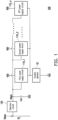
- the n th power supply circuit 110_n may drive the tunable element EE during an n th time period.
- the first power supply circuit 110_1 to the n th power supply circuit 110_n time-divisionally drive the tunable element EE during different time periods.
- the power supply circuit may be a driving circuit.
- the first power supply circuit 110_1 to the n th power supply circuit 110_n each receive a same high reference voltage VDD.
- the first time period and the second time period do not overlap.
- the first time period to the n th time period do not overlap each other.
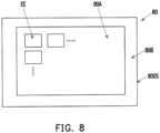
- a plurality of tunable elements EE may be disposed within the active area 80A of the substrate 80.
- the first power supply circuit 110_1 to the n th power supply circuit 110_n may be disposed within the active area 80A.
- the first power supply circuit 110_1 to the n th power supply circuit 110_n may be disposed within the peripheral area 80B.
- the substrate 80 may be a rigid substrate or a flexible substrate.
- the rigid substrate may be glass, and the flexible substrate may be plastics or a polymer, but the disclosure is not limited thereto.
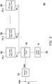
- FIG. 2 is a schematic diagram of an electronic device according to a second embodiment of the disclosure.
- an electronic device 200 includes the tunable element EE, a first power supply circuit 210_1 to an n th power supply circuit 210_n, a selection circuit 220, and the storage capacitor Cst.
- the first power supply circuit 210_1 to the n th power supply circuit 210_n time-divisionally drive the tunable element EE during different time periods.
- the scan transistor TS may be implemented with an N-type transistor.
- the scan transistor TS is an N-type thin film transistor or an NMOS transistor, for example.
- the scan transistor TS may be implemented with a P-type transistor.
- the scan transistor TS is turned off according to a high voltage value of the selection signal SS and turned on according to a low voltage value of the selection signal SS.
- the transistor is exemplified by an N-type transistor, but the disclosure is not limited thereto.
- a P-type transistor may also be adopted for the transistor, which will not be repeatedly described here.
- FIG. 3 is a circuit diagram of an electronic device according to the second embodiment of the disclosure
- FIG. 4 is a timing diagram according to the second embodiment of the disclosure.
- control signals VG1 to VGn may have a positive pulse during different time periods TT1 to TTn.
- the scan transistor TS may be turned on according to the selection signal SS during the scan time.
- the control signal VG1 has a positive pulse during the time period TT1.
- the control signal VG2 has a positive pulse during the time period TT2.
- the control signal VG3 has a positive pulse during the time period TT3.
- the control signal VGn has a positive pulse during the time period TTn.
- the time periods TT1 to TTn may be adjacent to each other and do not overlap each other.
- the first time period TT1 is adjacent to the second time period TT2. Therefore, the source follower circuits 212_1 to 212_n sequentially provide approximately the same driving electrical energy during the different time periods TT1 to TTn based on the control signals VG1 to VGn.
- the source follower circuit 212_1 is electrically connected to a first node ND1.
- the source follower circuit 212_1 is electrically connected to the tunable element EE through the first node ND1.
- the source follower circuit 212_1 includes a control terminal.
- a voltage at the first node ND1 may follow a voltage at the control terminal of the source follower circuit 212_1, and the voltage at the first node ND1 may be supplied to the tunable element EE.
- the source follower circuit 212_1 is implemented with a power supply transistor T1-1.
- a first terminal of the power supply transistor T1-1 receives the high reference voltage VDD.
- a second terminal of the power supply transistor T1-1 is electrically connected to the first node ND1.
- a control terminal of the power supply transistor T1-1 receives the control signal VG1.
- the power supply transistor T1-1 may be implemented with an N-type transistor.
- the power supply transistor T1-1 is an N-type thin film transistor or an NMOS transistor, for example.
- the compensation circuit 211_1 includes a compensation transistor T2-1.
- a first terminal of the compensation transistor T2-1 and a control terminal of the compensation transistor T2-1 are electrically connected to the second terminal of the scan transistor TS.
- a second terminal of the compensation transistor T2-1 is electrically connected to the first node ND1.
- the compensation transistor T2-1 is electrically connected between the second terminal of the scan transistor TS and the first node ND1 in a diode-connected manner.
- the first terminal of the scan transistor TS is electrically connected to the data line DL to receive the data voltage Vdata.
- the power supply transistor T1-2 may be implemented with an N-type transistor.
- the power supply transistor T1-2 is an N-type thin film transistor or an NMOS transistor, for example. Therefore, the voltage at the second node ND2 may follow a voltage value of the control signal VG2.
- the source follower circuit 212_n in the n th power supply circuit 210_n is electrically connected to the tunable element EE through an n th node NDn.
- the source follower circuit 212_n includes a control terminal. A voltage at the n th node NDn may follow a voltage at the control terminal of the source follower circuit 212_n, and the voltage at the n th node NDn may be supplied to the tunable element EE.
- the source follower circuit 212_n is implemented with a power supply transistor T1-n. A first terminal of the power supply transistor T1-n receives the high reference voltage VDD.
- the compensation circuit 211_n includes a compensation transistor T2-n.
- a first terminal of the compensation transistor T2-n and a control terminal of the compensation transistor T2-n are electrically connected to the second terminal of the scan transistor TS.
- a second terminal of the compensation transistor T2-n is electrically connected to the n th node NDn.
- the compensation circuit 211_n compensates for a voltage value at the n th node NDn with the data voltage Vdata during the n th time period, so that the voltage value at the n th node NDn reaches the design voltage value. Therefore, the voltage stress of the power supply transistor T1-n is not increased.
- the n th power supply circuit 310_n may provide an n th driving current IDn during an n th time period.
- the first driving current ID1 to the n th driving current IDn may be time-divisionally provided to the tunable element EE.
- the compensation circuit 320 is electrically connected to the first power supply circuit 310_1 to the n th power supply circuit 310_n, the selection circuit 330, and the tunable element EE.
- One of the first driving current ID1 to the n th driving current IDn may flow via the compensation circuit 320 through the tunable element EE during different time periods. Therefore, the compensation circuit 320 may receive one of the first driving current ID1 to the n th driving current IDn during different time periods.
- the compensation circuit 320 receives the first driving current ID1 and compensates for the first driving current ID1 flowing through the tunable element EE during the first time period, the compensation circuit 320 receives the second driving current ID2 and compensates for the second driving current ID2 flowing through the tunable element EE during the second time period, and so on and so forth.
- the selection circuit 330 is electrically connected to the data line DL.
- the selection circuit 330 receives the data voltage Vdata from the data line DL.
- the compensation circuit 320 compensates for the first driving current ID1 to the n th driving current IDn based on the data voltage Vdata.
- the current values of the first driving current ID1 to n th driving current IDn being compensated for are approximately the same as the driving current of the tunable element EE without an occurrence of leakage current.
- the selection circuit 330 and the compensation circuit 320 may be disposed within the active area 80A of the substrate 80, and the first power supply circuit 310_1 to the n th power supply circuit 310_n may be disposed within the peripheral area 80B.
- the control terminal of the power supply transistor T1-1 receives the control signal VG1.
- the power supply transistor T1-1 may provide the first driving current ID1 according to the control signal VG1 during the first time period.
- the second power supply circuit 310_2 includes the power supply transistor T1-2.
- the first terminal of the power supply transistor T1-2 receives the high reference voltage VDD.
- the second terminal of the power supply transistor T1-2 is electrically connected to the compensation circuit 320.
- the control terminal of the power supply transistor T1-2 receives the control signal VG2.
- the power supply transistor T1-2 may provide the second driving current ID2 according to the control signal VG2 during the second time period.
- the n th power supply circuit 310_n includes the power supply transistor T1-n.
- the first terminal of the power supply transistor T1-n receives the high reference voltage VDD.
- the second terminal of the power supply transistor T1-n is electrically connected to the compensation circuit 320.
- the control terminal of the power supply transistor T1-n receives the control signal VGn.
- the power supply transistor T1-n may provide the n th driving current IDn according to the control signal VGn during the n th time period.
- the selection circuit 330 includes the scan transistor TS.
- the first terminal of the scan transistor TS is electrically connected to the data line DL to receive the data voltage Vdata.
- the second terminal of the scan transistor TS is electrically connected to the compensation circuit 320.
- the control terminal of the scan transistor TS receives the selection signal SS.
- a first terminal of the compensation transistor TC is electrically connected to the second terminal of the bias transistor TB.
- a second terminal of the compensation transistor TC is electrically connected to a control terminal of the driving transistor TD.
- a control terminal of the compensation transistor TC receives the selection signal SS.
- the storage capacitor Cst is electrically connected to the first terminal of the bias transistor TB and the control terminal of the driving transistor TD.
- a first terminal of the reset transistor TR is electrically connected to the first terminal of the bias transistor TB.
- a second terminal of the reset transistor TR is electrically connected to the control terminal of the driving transistor TD.
- a control terminal of the reset transistor TR receives a reset signal SR.
- the control terminal of the driving transistor TD may receive the reference high voltage VDD.
- the voltage Vd at the first terminal of the driving transistor TD may be maintained in a working state.
- a voltage Vg at the control terminal of the driving transistor TD and the voltage Vd at the first terminal of the driving transistor TD are approximately equal to the reference high voltage VDD.
- the bias transistor TB is turned off according to the bias signal SB having a low voltage level.
- the scan transistor TS and the compensation transistor TC are turned on according to the selection signal SS having a high voltage level, so that the driving transistor TD is operated in a diode-connected manner.
- the data line DL may provide the data voltage Vdata through the scan transistor TS, the driving transistor TD, and the compensation transistor TC to the control terminal of the driving transistor TD. Therefore, the voltage Vg at the control terminal of the driving transistor TD may be a voltage of Vdata +
- the voltage Vd at the first terminal of the driving transistor TD is also a voltage of Vdata +
- the bias transistor TB is turned on according to the bias signal SB having a high voltage level.
- the scan transistor TS and the compensation transistor TC are turned off according to the selection signal SS having a low voltage level. Since the bias transistor TB is turned on, the voltage Vd at the first terminal of the driving transistor TD is the high reference voltage VDD.
- the voltage Vg of the control terminal of the driving transistor TD is maintained at the voltage of Vdata +
- the voltage Vs at the second terminal of the driving transistor TD may be the data voltage Vdata.
- the tunable element EE works in a working state, and the second terminal of the driving transistor TD provides the received driving current to the tunable element EE according to the working voltage VDD.
- a voltage at the node N1 may be dropped.
- the voltage Vs at the second terminal of the driving transistor TD may also be dropped.
- the voltage Vg at the control terminal of the driving transistor TD may be a voltage of Vdata +
Landscapes
- Engineering & Computer Science (AREA)
- Physics & Mathematics (AREA)
- Computer Hardware Design (AREA)
- General Physics & Mathematics (AREA)
- Theoretical Computer Science (AREA)
- Electronic Switches (AREA)
- Control Of Indicators Other Than Cathode Ray Tubes (AREA)
- Power Sources (AREA)
- Direct Current Feeding And Distribution (AREA)
- Logic Circuits (AREA)
Applications Claiming Priority (2)
| Application Number | Priority Date | Filing Date | Title |
|---|---|---|---|
| US202163251046P | 2021-10-01 | 2021-10-01 | |
| CN202210801664.2A CN115909923A (zh) | 2021-10-01 | 2022-07-08 | 电子装置 |
Publications (2)
| Publication Number | Publication Date |
|---|---|
| EP4160584A2 true EP4160584A2 (de) | 2023-04-05 |
| EP4160584A3 EP4160584A3 (de) | 2023-05-31 |
Family
ID=83400613
Family Applications (1)
| Application Number | Title | Priority Date | Filing Date |
|---|---|---|---|
| EP22196833.2A Pending EP4160584A3 (de) | 2021-10-01 | 2022-09-21 | Elektronische vorrichtung |
Country Status (3)
| Country | Link |
|---|---|
| US (2) | US11990906B2 (de) |
| EP (1) | EP4160584A3 (de) |
| TW (2) | TWI880104B (de) |
Family Cites Families (13)
| Publication number | Priority date | Publication date | Assignee | Title |
|---|---|---|---|---|
| GB0130176D0 (en) * | 2001-12-18 | 2002-02-06 | Koninkl Philips Electronics Nv | Electroluminescent display device |
| US6998788B2 (en) * | 2003-06-11 | 2006-02-14 | Au Optronics Corporation | Architecture of data driver applied at display elements with current-driven pixels |
| TWI258098B (en) * | 2004-12-31 | 2006-07-11 | Pixart Imaging Inc | Method and related apparatus for decreasing delay time and power consumption of a wireless mouse |
| US9741309B2 (en) * | 2009-01-22 | 2017-08-22 | Semiconductor Energy Laboratory Co., Ltd. | Method for driving display device including first to fourth switches |
| JP5227245B2 (ja) * | 2009-04-28 | 2013-07-03 | 東京エレクトロン株式会社 | プラズマ処理装置 |
| US9214475B2 (en) * | 2013-07-09 | 2015-12-15 | Pixtronix, Inc. | All N-type transistor inverter circuit |
| KR102197137B1 (ko) * | 2014-05-29 | 2020-12-31 | 에스케이하이닉스 주식회사 | 반도체 장치 및 이를 포함하는 반도체 시스템 |
| CN104700778B (zh) | 2015-03-27 | 2017-06-27 | 深圳市华星光电技术有限公司 | Amoled像素驱动电路及像素驱动方法 |
| KR20180095836A (ko) * | 2015-12-18 | 2018-08-28 | 가부시키가이샤 한도오따이 에네루기 켄큐쇼 | 반도체 장치 및 상기 반도체 장치를 포함한 표시 장치 |
| CN106097959A (zh) | 2016-06-02 | 2016-11-09 | 京东方科技集团股份有限公司 | 像素单元及其驱动方法、像素驱动电路和显示装置 |
| US11049658B2 (en) | 2016-12-22 | 2021-06-29 | Kymeta Corporation | Storage capacitor for use in an antenna aperture |
| US10755643B2 (en) * | 2017-09-29 | 2020-08-25 | Sharp Kabushiki Kaisha | Display device and driving method thereof |
| CN108520716B (zh) * | 2018-04-12 | 2019-10-01 | 京东方科技集团股份有限公司 | 一种像素电路单元及驱动方法、显示面板、显示装置 |
-
2022
- 2022-08-01 TW TW111128778A patent/TWI880104B/zh active
- 2022-08-01 TW TW114108536A patent/TW202526904A/zh unknown
- 2022-09-15 US US17/945,092 patent/US11990906B2/en active Active
- 2022-09-21 EP EP22196833.2A patent/EP4160584A3/de active Pending
-
2024
- 2024-05-14 US US18/663,116 patent/US12328122B2/en active Active
Also Published As
| Publication number | Publication date |
|---|---|
| US20230108090A1 (en) | 2023-04-06 |
| US20240297638A1 (en) | 2024-09-05 |
| TW202316404A (zh) | 2023-04-16 |
| US12328122B2 (en) | 2025-06-10 |
| EP4160584A3 (de) | 2023-05-31 |
| TWI880104B (zh) | 2025-04-11 |
| TW202526904A (zh) | 2025-07-01 |
| US11990906B2 (en) | 2024-05-21 |
Similar Documents
| Publication | Publication Date | Title |
|---|---|---|
| US20230410729A1 (en) | Pixel circuit, driving method of pixel circuit, and display panel | |
| US10964261B2 (en) | Pixel circuitry, driving method thereof and display device | |
| US10032838B2 (en) | AMOLED pixel driving circuit and pixel driving method | |
| US20050052377A1 (en) | Pixel driving circuit and method for use in active matrix OLED with threshold voltage compensation | |
| WO2016127644A1 (en) | Pixel compensating circuits, related display apparatus and method for driving the same | |
| EP3982352B1 (de) | Treiberschaltung und elektronische vorrichtung zur ansteuerung einer lichtemittierenden einheit | |
| CN113066427B (zh) | 像素电路、发光显示装置及其驱动方法 | |
| US20240212583A1 (en) | Pixel driving circuit, driving method thereof, and display panel | |
| US20250241128A1 (en) | Display panel and display device | |
| CN115171608B (zh) | 驱动电路、驱动方法及显示面板 | |
| US12159568B2 (en) | Pixel driving circuit and driving method thereof, and display panel | |
| CN117475904A (zh) | 像素驱动电路及显示面板 | |
| KR20210092306A (ko) | 픽셀 회로, 디스플레이 장치 및 픽셀 회로의 구동 방법 | |
| US12328122B2 (en) | Electronic device | |
| CN115909923A (zh) | 电子装置 | |
| CN117854408A (zh) | 调变装置 | |
| CN115148152A (zh) | 显示面板及其温度侦测方法、显示装置 | |
| US12307984B2 (en) | Modulating device | |
| US20250240011A1 (en) | Electronic circuit | |
| US20250386407A1 (en) | Electronic device | |
| US20260134841A1 (en) | Subpixel and Display Device Having the Same | |
| KR20260068970A (ko) | 서브픽셀 및 이를 포함하는 표시 장치 | |
| TW202343406A (zh) | 電子裝置 | |
| TW202343809A (zh) | 電子裝置以及二極管 | |
| CN117641659A (zh) | 发光装置 |
Legal Events
| Date | Code | Title | Description |
|---|---|---|---|
| PUAI | Public reference made under article 153(3) epc to a published international application that has entered the european phase |
Free format text: ORIGINAL CODE: 0009012 |
|
| STAA | Information on the status of an ep patent application or granted ep patent |
Free format text: STATUS: THE APPLICATION HAS BEEN PUBLISHED |
|
| AK | Designated contracting states |
Kind code of ref document: A2 Designated state(s): AL AT BE BG CH CY CZ DE DK EE ES FI FR GB GR HR HU IE IS IT LI LT LU LV MC MK MT NL NO PL PT RO RS SE SI SK SM TR |
|
| PUAL | Search report despatched |
Free format text: ORIGINAL CODE: 0009013 |
|
| AK | Designated contracting states |
Kind code of ref document: A3 Designated state(s): AL AT BE BG CH CY CZ DE DK EE ES FI FR GB GR HR HU IE IS IT LI LT LU LV MC MK MT NL NO PL PT RO RS SE SI SK SM TR |
|
| RIC1 | Information provided on ipc code assigned before grant |
Ipc: G09G 3/32 20160101AFI20230426BHEP |
|
| STAA | Information on the status of an ep patent application or granted ep patent |
Free format text: STATUS: REQUEST FOR EXAMINATION WAS MADE |
|
| 17P | Request for examination filed |
Effective date: 20231127 |
|
| RBV | Designated contracting states (corrected) |
Designated state(s): AL AT BE BG CH CY CZ DE DK EE ES FI FR GB GR HR HU IE IS IT LI LT LU LV MC MK MT NL NO PL PT RO RS SE SI SK SM TR |
|
| STAA | Information on the status of an ep patent application or granted ep patent |
Free format text: STATUS: EXAMINATION IS IN PROGRESS |
|
| 17Q | First examination report despatched |
Effective date: 20251223 |