EP4160303B1 - Substrate and electronic device - Google Patents
Substrate and electronic device Download PDFInfo
- Publication number
- EP4160303B1 EP4160303B1 EP21813346.0A EP21813346A EP4160303B1 EP 4160303 B1 EP4160303 B1 EP 4160303B1 EP 21813346 A EP21813346 A EP 21813346A EP 4160303 B1 EP4160303 B1 EP 4160303B1
- Authority
- EP
- European Patent Office
- Prior art keywords
- circular arc
- substrate
- line segment
- straight line
- cutting section
- Prior art date
- Legal status (The legal status is an assumption and is not a legal conclusion. Google has not performed a legal analysis and makes no representation as to the accuracy of the status listed.)
- Active
Links
Images







Classifications
-
- B—PERFORMING OPERATIONS; TRANSPORTING
- B23—MACHINE TOOLS; METAL-WORKING NOT OTHERWISE PROVIDED FOR
- B23K—SOLDERING OR UNSOLDERING; WELDING; CLADDING OR PLATING BY SOLDERING OR WELDING; CUTTING BY APPLYING HEAT LOCALLY, e.g. FLAME CUTTING; WORKING BY LASER BEAM
- B23K26/00—Working by laser beam, e.g. welding, cutting or boring
- B23K26/36—Removing material
- B23K26/38—Removing material by boring or cutting
-
- B—PERFORMING OPERATIONS; TRANSPORTING
- B23—MACHINE TOOLS; METAL-WORKING NOT OTHERWISE PROVIDED FOR
- B23K—SOLDERING OR UNSOLDERING; WELDING; CLADDING OR PLATING BY SOLDERING OR WELDING; CUTTING BY APPLYING HEAT LOCALLY, e.g. FLAME CUTTING; WORKING BY LASER BEAM
- B23K26/00—Working by laser beam, e.g. welding, cutting or boring
- B23K26/70—Auxiliary operations or equipment
- B23K26/702—Auxiliary equipment
-
- B—PERFORMING OPERATIONS; TRANSPORTING
- B23—MACHINE TOOLS; METAL-WORKING NOT OTHERWISE PROVIDED FOR
- B23K—SOLDERING OR UNSOLDERING; WELDING; CLADDING OR PLATING BY SOLDERING OR WELDING; CUTTING BY APPLYING HEAT LOCALLY, e.g. FLAME CUTTING; WORKING BY LASER BEAM
- B23K2101/00—Articles made by soldering, welding or cutting
- B23K2101/36—Electric or electronic devices
-
- B—PERFORMING OPERATIONS; TRANSPORTING
- B23—MACHINE TOOLS; METAL-WORKING NOT OTHERWISE PROVIDED FOR
- B23K—SOLDERING OR UNSOLDERING; WELDING; CLADDING OR PLATING BY SOLDERING OR WELDING; CUTTING BY APPLYING HEAT LOCALLY, e.g. FLAME CUTTING; WORKING BY LASER BEAM
- B23K2103/00—Materials to be soldered, welded or cut
- B23K2103/50—Inorganic materials other than metals or composite materials
- B23K2103/56—Inorganic materials other than metals or composite materials being semiconducting
-
- B—PERFORMING OPERATIONS; TRANSPORTING
- B32—LAYERED PRODUCTS
- B32B—LAYERED PRODUCTS, i.e. PRODUCTS BUILT-UP OF STRATA OF FLAT OR NON-FLAT, e.g. CELLULAR OR HONEYCOMB, FORM
- B32B38/00—Ancillary operations in connection with laminating processes
- B32B38/10—Removing layers, or parts of layers, mechanically or chemically
-
- G—PHYSICS
- G02—OPTICS
- G02F—OPTICAL DEVICES OR ARRANGEMENTS FOR THE CONTROL OF LIGHT BY MODIFICATION OF THE OPTICAL PROPERTIES OF THE MEDIA OF THE ELEMENTS INVOLVED THEREIN; NON-LINEAR OPTICS; FREQUENCY-CHANGING OF LIGHT; OPTICAL LOGIC ELEMENTS; OPTICAL ANALOGUE/DIGITAL CONVERTERS
- G02F1/00—Devices or arrangements for the control of the intensity, colour, phase, polarisation or direction of light arriving from an independent light source, e.g. switching, gating or modulating; Non-linear optics
- G02F1/01—Devices or arrangements for the control of the intensity, colour, phase, polarisation or direction of light arriving from an independent light source, e.g. switching, gating or modulating; Non-linear optics for the control of the intensity, phase, polarisation or colour
- G02F1/13—Devices or arrangements for the control of the intensity, colour, phase, polarisation or direction of light arriving from an independent light source, e.g. switching, gating or modulating; Non-linear optics for the control of the intensity, phase, polarisation or colour based on liquid crystals, e.g. single liquid crystal display cells
- G02F1/1303—Apparatus specially adapted to the manufacture of LCDs
-
- G—PHYSICS
- G02—OPTICS
- G02F—OPTICAL DEVICES OR ARRANGEMENTS FOR THE CONTROL OF LIGHT BY MODIFICATION OF THE OPTICAL PROPERTIES OF THE MEDIA OF THE ELEMENTS INVOLVED THEREIN; NON-LINEAR OPTICS; FREQUENCY-CHANGING OF LIGHT; OPTICAL LOGIC ELEMENTS; OPTICAL ANALOGUE/DIGITAL CONVERTERS
- G02F1/00—Devices or arrangements for the control of the intensity, colour, phase, polarisation or direction of light arriving from an independent light source, e.g. switching, gating or modulating; Non-linear optics
- G02F1/01—Devices or arrangements for the control of the intensity, colour, phase, polarisation or direction of light arriving from an independent light source, e.g. switching, gating or modulating; Non-linear optics for the control of the intensity, phase, polarisation or colour
- G02F1/13—Devices or arrangements for the control of the intensity, colour, phase, polarisation or direction of light arriving from an independent light source, e.g. switching, gating or modulating; Non-linear optics for the control of the intensity, phase, polarisation or colour based on liquid crystals, e.g. single liquid crystal display cells
- G02F1/133—Constructional arrangements; Operation of liquid crystal cells; Circuit arrangements
- G02F1/1333—Constructional arrangements; Manufacturing methods
-
- G—PHYSICS
- G02—OPTICS
- G02F—OPTICAL DEVICES OR ARRANGEMENTS FOR THE CONTROL OF LIGHT BY MODIFICATION OF THE OPTICAL PROPERTIES OF THE MEDIA OF THE ELEMENTS INVOLVED THEREIN; NON-LINEAR OPTICS; FREQUENCY-CHANGING OF LIGHT; OPTICAL LOGIC ELEMENTS; OPTICAL ANALOGUE/DIGITAL CONVERTERS
- G02F1/00—Devices or arrangements for the control of the intensity, colour, phase, polarisation or direction of light arriving from an independent light source, e.g. switching, gating or modulating; Non-linear optics
- G02F1/01—Devices or arrangements for the control of the intensity, colour, phase, polarisation or direction of light arriving from an independent light source, e.g. switching, gating or modulating; Non-linear optics for the control of the intensity, phase, polarisation or colour
- G02F1/13—Devices or arrangements for the control of the intensity, colour, phase, polarisation or direction of light arriving from an independent light source, e.g. switching, gating or modulating; Non-linear optics for the control of the intensity, phase, polarisation or colour based on liquid crystals, e.g. single liquid crystal display cells
- G02F1/133—Constructional arrangements; Operation of liquid crystal cells; Circuit arrangements
- G02F1/1333—Constructional arrangements; Manufacturing methods
- G02F1/133302—Rigid substrates, e.g. inorganic substrates
-
- G—PHYSICS
- G02—OPTICS
- G02F—OPTICAL DEVICES OR ARRANGEMENTS FOR THE CONTROL OF LIGHT BY MODIFICATION OF THE OPTICAL PROPERTIES OF THE MEDIA OF THE ELEMENTS INVOLVED THEREIN; NON-LINEAR OPTICS; FREQUENCY-CHANGING OF LIGHT; OPTICAL LOGIC ELEMENTS; OPTICAL ANALOGUE/DIGITAL CONVERTERS
- G02F2201/00—Constructional arrangements not provided for in groups G02F1/00 - G02F7/00
- G02F2201/56—Substrates having a particular shape, e.g. non-rectangular
-
- H—ELECTRICITY
- H04—ELECTRIC COMMUNICATION TECHNIQUE
- H04M—TELEPHONIC COMMUNICATION
- H04M1/00—Substation equipment, e.g. for use by subscribers
- H04M1/02—Constructional features of telephone sets
- H04M1/03—Constructional features of telephone transmitters or receivers, e.g. telephone hand-sets
-
- H—ELECTRICITY
- H10—SEMICONDUCTOR DEVICES; ELECTRIC SOLID-STATE DEVICES NOT OTHERWISE PROVIDED FOR
- H10K—ORGANIC ELECTRIC SOLID-STATE DEVICES
- H10K59/00—Integrated devices, or assemblies of multiple devices, comprising at least one organic light-emitting element covered by group H10K50/00
- H10K59/10—OLED displays
Definitions
- Embodiments of the present disclosure relate to a substrate, and an electronic device.
- a substrate motherboard is first cut into a plurality of separate substrates using a cutter wheel, and then a corner of the substrate is cut using laser light through an outer cutting process.
- the outer cutting process means that the laser light is used to directly cut the substrate from an edge of the substrate to another edge of the substrate, so that the corner of the substrate is cut off.
- the substrate is provided with electronic elements therein, when the laser light cuts to the edge of the substrate, the edge of the substrate will refract the laser light to an inside of the substrate. As a result, the laser light is reflected back and forth inside the substrate. In this case, the laser light is easily reflected to the electronic elements of the substrate, which easily causes the electronic elements to be burned, resulting in product defects.
- US 2020/070285 A1 provides an irregularly-shaped display panel and a cutting method.
- the display panel includes a display region and a non-display region surrounding the display region.
- the non-display region includes at least one irregularly-shaped boundary.
- the irregularly-shaped display panel further includes a substrate and the substrate includes a base substrate.
- the non-display region includes laser cutting trajectories. An orthographic projection of each of the laser cutting trajectories to the base substrate at least partially overlaps an orthographic projection of a corresponding irregularly-shaped boundary.
- Each of the laser cutting trajectories includes a cutting entry point and a cutting exit point at two ends thereof, and at least one of the cutting entry point and the cutting exit point does not overlap the orthographic projection of the corresponding irregularly-shaped boundary.
- US 2019/181387 A1 provides a display device.
- the display device includes first and second regions connected to each other. When viewed in a plan view, the first and second regions have a curved edge and a rectilinear edge, respectively.
- a side surface of the first region may include a center region having a rectilinear shape and a side surface of the second region may include a center region having a curved shape.
- the side surface of the first region has a first roughness
- a side surface of the second region has a second roughness that is smoother than the first roughness.
- US 2019/369667 A1 provides a display device.
- the display device including a linear portion and a curved portion, includes a first substrate including a first surface and a second surface opposite the first surface; a second substrate including a third surface and a fourth surface opposite the third surface; and a display panel disposed between the first surface of the first substrate and the fourth surface of the second substrate.
- An outer surface adjacent to the first surface of the first substrate protrudes outward from an outer surface adjacent to the second surface of the first substrate, and a first width of a region of the first surface of the first substrate that does not overlap with the second surface in the linear portion is greater than a second width of a region of the first surface of the first substrate that does not overlap with the second surface of the first substrate in the curved portion.
- CN 111151894 A provides a special-shaped display panel and a cutting method thereof.
- the cutting method of the special-shaped display panel comprises the steps of providing a to-be-cut special-shaped display panel, cutting special-shaped corners and carrying out edge modification cutting, and glass residues at the arc ends of round corners can be removed to form smooth special-shaped corners.
- the special-shaped display panel is manufactured through the cutting method and comprises at least one special-shaped corner, and the special-shaped corner is formed by overlapping a first laser cutting track and a second laser cutting track.
- the present disclosure provides a substrate which is defined by claim 1.
- the present disclosure provides an electronic device which is defined by claim 13.
- the substrate 1 includes at least two edges 11 and at least one end portion 12, and each end portion 12 is connected to two adjacent edges 11.
- FIG. 1 only schematically illustrates one end portion 12 of the substrate 1, and does not limit the number of end portions 12 of the substrate 1. That is, in practical applications, the substrate 1 may be provided with only one end portion 12, or two or more end portions 12.
- each end portion 12 is connected to two edges 11 adjacent thereto.
- the number of the end portions of the substrate 1 should be four.
- each end portion 12 includes a cutting section 121 and two breaking section 122.
- An end of the cutting section 121 is connected to one of the two adjacent edges 11 through a breaking section 122, another end of the cutting section 121 is connected to another edge 11 of the two adjacent edges 11 through another breaking section 122.
- the cutting section 121 is configured to be formed through cutting of a tool.
- the tool may be a tool with a cutting function such as a laser cutting machine.
- the cutting section 121 of the substrate 1 may be formed through cutting using laser light of the laser cutting machine.
- the breaking sections 122 are configured to be formed under an action of a physical force.
- the physical force may be gravity or a pressure exerted by an external object. In a case where the physical force is the gravity, after the cutting section 121 is formed through cutting of the tool, a corner, which is to be removed, of a substrate will naturally be broken under the action of the gravity, and thus the substrate 1 is formed.
- the physical force is the pressure exerted by the external object
- the cutting section 121 is formed through cutting of the tool
- a corner, which is to be removed, of a substrate will naturally be broken under the action of the pressure exerted by the external object (such as a human hand or a mechanical equipment), and thus the substrate 1 is formed.
- the end portion 12 of the substrate 1 since the end portion 12 of the substrate 1 includes both the cutting section 121 and the two breaking sections 122 located at both ends of the cutting section 121, when the corner, which is to be removed, of the substrate is removed, the laser light will not be directed to edges 11 of the substrate 1. As a result, the laser light will not be refracted to an inside of the substrate 1 through the edges 11 of the substrate 1, and in turn, the laser light will not be reflected back and forth inside the substrate 1, which may prevent the laser light from being reflected to electronic elements of the substrate 1. Therefore, it is beneficial to prevent the electronic elements from being burned, thereby reducing product defects.
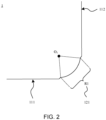
- an orthographic projection of the cutting section 121 on a plane where the substrate 1 is located includes a first circular arc R1, and an arc center O 1 of the first circular arc R1 is located at an inside of the substrate 1. Therefore, a relatively regular rounded corner of the substrate 1 may be formed after a substrate whose corner is to be removed is cut and the corner to be removed of the substrate is broken, which may improve universality of the substrate 1.
- the orthographic projection of the cutting section 121 on the plane where the substrate 1 is located may include only the first circular arc R1; or besides the first circular arc R1, the orthographic projection of the cutting section 121 on the plane where the substrate 1 is located further includes other portion(s) (e.g., as shown in FIGS. 3A , 3B , 4A , 4B and FIGS. 5 to 7 , including at least one of a second circular arc R2 and a third circular arc R3, and may further include a fourth circular arc R4, a fifth circular arc R5, a first straight line segment L1 and a second straight line segment L2).
- other portion(s) e.g., as shown in FIGS. 3A , 3B , 4A , 4B and FIGS. 5 to 7 , including at least one of a second circular arc R2 and a third circular arc R3, and may further include a fourth circular arc R4, a fifth circular arc R5, a first straight line segment L1 and
- a shortest distance between each point on the orthographic projection, on the plane where the substrate 1 is located, of the cutting section 121 and a circle where the first circular arc R1 is located is less than or equal to a first limit value.
- the first limit value may be related to a cutting accuracy of the substrate required by a product. For example, in a case where the cutting accuracy required by the product does not exceed h (that is, a cutting offset of the cutting section 121 does not exceed h), the first limit value may be set to be less than or equal to h.
- the first limit value may be set to be approximately equal to 0.8h.
- the first limit value is approximately equal to 0.04 mm.
- the expression "approximately equal to” refers to being within a range of plus or minus ten percent. That is, in the case where h is equal to 0.05 mm, the first limit value may be in a range of 0.036 mm to 0.044 mm, inclusive. In this case, it is easier to obtain the cutting section 121 that meets the cutting accuracy, and is beneficial to ameliorate a problem that the cutting section 121 is cut more or less.
- a dimension of each breaking section 122 in a first direction is a second limit value d.
- the first direction is a direction E parallel to the plane where the substrate 1 is located and perpendicular to an edge 111 that is connected to the breaking section 1221, or a direction F parallel to the plane where the substrate 1 is located and perpendicular to another edge 112 that is connected to another breaking section 1222.
- the breaking sections 122 may be formed under the action of the physical force after the cutting section 121 is formed through cutting.
- the second limit value d is in a range of 0.06 mm to 0.1 mm, inclusive.
- the second limit value d may be in a range of 0.06 mm to 0.08 mm.
- a width of the breaking section 1221 connected to the edge 111 in the first direction E may be 0.06 mm, 0.07 mm or 0.1 mm, etc.
- a width of the another breaking section 1222 connected to the edge 112 in the second direction F may be 0.06 mm, 0.07 mm or 0.1 mm, etc.
- some embodiments of the present disclosure further modify the cutting section 121 of the substrate 1.
- the cutting section 121 of the substrate 1 includes, but is not limited to, a cutting section 121 in the following embodiments.
- the orthographic projection of the cutting section 121 on the plane where the substrate 1 is located further includes a second circular arc R2 and/or a third circular arc R3.
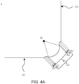
- a first end of the second circular arc R2 is connected to an orthographic projection of a breaking section 122 (i.e., one of the two breaking sections 122 included in the end portion 12 corresponding to the second circular arc R2) on the plane where the substrate 1 is located, and a second end of the second circular arc R2 is directly or indirectly connected to a first end of the first circular arc R1 (e.g., FIG. 3A shows a case where the second end of the second circular arc R2 is directly connected to the first end of the first circular arc R1, and FIGS. 4A , 5 and 6 show a case where the second end of the second circular arc R2 is indirectly connected to the first end of the first circular arc R1).
- a breaking section 122 i.e., one of the two breaking sections 122 included in the end portion 12 corresponding to the second circular arc R2
- FIGS. 4A , 5 and 6 show a case where the second end of the second circular arc R2 is indirectly connected to the first end of the
- An arc center of the second circular arc R2 is located at an outside of the substrate 1.
- a first end of the third circular arc R3 is connected to an orthographic projection of another breaking section 122 (i.e., the other of the two breaking sections 122 included in the end portion 12 corresponding to the third circular arc R3) on the plane where the substrate 1 is located, and a second end of the third circular arc R3 is directly or indirectly connected to a second end of the first circular arc R1 (e.g., FIG. 3A shows a case where the second end of the third circular arc R3 is directly connected to the second end of the first circular arc R1, and FIGS. 4A , 5 and 6 show a case where the second end of the third circular arc R3 is indirectly connected to the second end of the first circular arc R1).
- An arc center of the third circular arc R3 is located at the outside of the substrate 1.
- a position of the arc center O 1 of the first circular arc R1 and a radius r 1 of the first circular arc R1 are known.
- a first auxiliary line m1 and a second auxiliary line m2 are firstly drawn on a side of any one edge 11 close to the first circular arc R1.
- the first auxiliary line m1 is parallel to an orthographic projection of the edge 11 on the plane where the substrate 1 is located, and a distance between the first auxiliary line m1 and the orthographic projection of the edge 11 on the plane where the substrate 1 is located is the second limit value (e.g., the second limit value may be in the range of 0.06 mm to 0.1 mm, inclusive);
- the second auxiliary line m2 is parallel to the orthographic projection of the edge 11 on the plane where the substrate 1 is located, and a distance between the second auxiliary line m2 and the orthographic projection of the edge 11 on the plane where the substrate 1 is located is a sum of the second limit value and the first limit value (e.g., the first limit value may be in the range of 0.036 mm to 0.044 mm, inclusive).
- an intersection point is determined as a first position point T 1 , the intersection point being an intersection point closest to the first circular arc R1 in all intersection points of the circle where the first circular arc R1 is located and the second auxiliary line m2; and an intersection point is determined as a second position point T 2 , the intersection point being an intersection point closest to the first circular arc R1 in all intersection points of the circle where the first circular arc R1 is located and the first auxiliary line m1.
- a third auxiliary line m3 passing through the first position point T 1 is drawn, and an angle between the third auxiliary line m3 and the first auxiliary line m1 is a preset angle ⁇ ; the third auxiliary line m3 and the first auxiliary line m1 intersect at a third position point T 3 .
- a value of the preset angle ⁇ is not limited in the embodiments, as long as it is ensured that the third position point T 3 is between the first position point T 1 and the second position point T 2 in a direction parallel to the first auxiliary line m1.
- the preset angle ⁇ may be in a range of 30° to 60°, inclusive.
- a radius of the second circular arc is r 21
- a radius of the third circular arc is r 21 .
- k 1 is in a range of 1 to 2, inclusive; r 1 is the radius of the first circular arc R1; s is the first limit value; ⁇ is a central angle corresponding to an auxiliary circular arc, the auxiliary circular arc is obtained by extending the first circular arc R1, and distances from two opposite ends of the auxiliary circular arc to the two edges 11 adjacent to the auxiliary circular arc are each equal to the second limit value.
- the first limit value and the second limit value have been described above, and will not be repeated here.
- the radius r 21 of the second circular arc R2 or the third circular arc R3 is equal to a length of a line segment T 1 T 3 multiplied by tan ⁇ 1 .
- a length of the line segment T 1 T 3 is equal to 2 • s , where s is the first limit value.
- the central angle of the second circular arc R2 or the third circular arc R3 is equal to (2 ⁇ (90° - ⁇ 1 )).
- the central angle of the second circular arc R2 may be in a range of 25° to 40°, inclusive; and the central angle of the third circular arc R3 may also be in the range of 25° to 40°, inclusive.
- the orthographic projection of the cutting section 121 on the plane where the substrate is located further includes the first straight line segment L1 and/or the second straight line segment L2.
- a first end of the first straight segment L1 is connected to the second end of the second circular arc R2, and a second end of the first straight segment L1 is connected to the first end of the first circular arc R1.
- a smooth transition may be achieved between the first circular arc R1 and the second circular arc R2 through the first straight line segment L1, so that the cutting section 121 is less likely to have sharp corners, which may better meet use requirements of the substrate.
- a first end of the second straight line segment L2 is connected to the second end of the third circular arc R3, and a second end of the second straight line segment L2 is connected to the second end of the first circular arc R1.
- a smooth transition may be achieved between the first circular arc R1 and the third circular arc R3 through the second straight line segment L2, so that the cutting section 121 is less likely to have sharp corners, which may better meet use requirements of the substrate.
- the first straight line segment L1 is tangent to both the second circular arc R2 and the first circular arc R1
- the second straight line segment L2 is tangent to both the third circular arc R3 and the first circular arc R1.
- a smoother transition effect may be achieved between the first circular arc R1 and the second circular arc R2, and/or between the first circular arc R1 and the third circular arc R3.
- a fourth auxiliary line m4 a fifth auxiliary line m5 and a sixth auxiliary line m6 are firstly drawn on a side of any one edge 11 close to the cutting section 121.
- the fourth auxiliary line m4 is parallel to an orthographic projection of the edge 11 on the plane where the substrate 1 is located, and a distance between the fourth auxiliary line m4 and the orthographic projection of the edge 11 on the plane where the substrate 1 is located is the second limit value (e.g., the second limit value may be in the range of 0.06 mm to 0.1 mm, inclusive);
- the fifth auxiliary line m5 is parallel to the orthographic projection of the edge 11 on the plane where the substrate 1 is located, and a distance between the fifth auxiliary line m5 and the orthographic projection of the edge 11 on the plane where the substrate 1 is located is the sum of the second limit value and the first limit value (e.g., the first limit value may be in the range of 0.036 mm to 0.044 mm, inclusive);
- the sixth auxiliary line m6 is parallel to the orthographic projection of the edge 11 on the plane where the substrate 1 is located, and a distance between the sixth auxiliary line m6 and the orthographic projection of the edge 11 on the plane
- the third limit value is approximately equal to 0.05 mm.
- the term “approximately” means that the third limit value may be plus or minus ten percent on a basis of 0.05 mm.
- an intersection point is determined as a fourth position point T 4 , the intersection point being an intersection point closest to the first circular arc R1 in all intersection points of the circle where the first circular arc R1 is located and the fourth auxiliary line m4; an intersection point is determined as a fifth position point T 5 , the intersection point being an intersection point closest to the first circular arc R1 in all intersection points of the circle where the first circular arc R1 is located and the fifth auxiliary line m5; and an intersection point is determined as a sixth position point T 6 , the intersection point being an intersection point closest to the first circular arc R1 in all intersection points of the circle where the first circular arc R1 is located and the sixth auxiliary line m6.
- a seventh auxiliary line m7 passing through the fifth position point T 5 is drawn, and an angle between the seventh auxiliary line m7 and the fourth auxiliary line m4 is a preset angle ⁇ ; the seventh auxiliary line m7 and the fourth auxiliary line m4 intersect at a seventh position point T 7 .
- a value of the preset angle ⁇ is not limited in the embodiments, as long as it is ensured that the seventh position point T 7 is between the fourth position point T 4 and the fifth position point T 5 in a direction parallel to the fourth auxiliary line m4.
- the preset angle ⁇ may be in a range of 30° to 60°, inclusive.
- a circular arc (i.e., the second circular arc R2 or the third circular arc R3) passing through the seventh point T 7 and tangent to both the seventh auxiliary line m7 and a line segment T 5 T 6 is drawn.
- a portion of the line segment T 5 T 6 between the drawn circular arc (i.e. the second circular arc R2 or the third circular arc R3) and the first circular arc R1 is the first straight line segment L1 or the second straight line segment L2.
- a radius of the second circular arc R2 is r 22
- a radius of the third circular arc R3 is r 22 .
- k 1 is in the range of 1 to 2, inclusive; r 1 is the radius of the first circular arc R1; s is the first limit value; ⁇ is a central angle corresponding to an auxiliary circular arc, the auxiliary circular arc is obtained by extending the first circular arc R1, and distances from two opposite ends of the auxiliary circular arc to the two edges 11 adjacent to the auxiliary circular arc are each equal to a second limit value; and u is the third limit value.
- the first limit value, the second limit value and the third limit value have been described above, and will not be repeated here.
- the radius r 22 of the second circular arc is equal to a length of a line segment T 5 T 7 multiplied by tan ⁇ 2
- the radius r 22 of the third circular arc is equal to the length of the line segment T 5 T 7 multiplied by tan ⁇ 2
- the length of the line segment T 5 T 7 is equal to 2 • s , s being the first limit value as described above.
- a length of a line segment O 1 B 1 is r 1 ⁇ cos(45°- ⁇ /2)-s
- a length of a line segment O 1 B 2 is r 1 ⁇ cos(45°- ⁇ /2)-s-u.
- a length of a line segment T 5 B 1 is r 1 2 ⁇ r 1 • cos 45 ° ⁇ ⁇ / 2 ⁇ s 2
- a length of a line segment T 6 B 2 is ⁇ (r 1 2 - [r 1 ⁇ cos (45 - ⁇ /2) - s - u] 2 ) .
- r 22 k 1 • 2 • s • tan 1 2 135 ° + arctan u r 1 2 ⁇ r 1 • cos 45 ° ⁇ ⁇ / 2 ⁇ s ⁇ u 2 ⁇ r 1 2 ⁇ r 1 • cos 45 ° ⁇ ⁇ /2 ⁇ s 2
- k 1 is designed in the range of 1 to 2, inclusive.
- the central angle of the second circular arc R2 or the third circular arc R3 is equal to (2 ⁇ (90° - ⁇ 2 )).
- the central angle of the second circular arc R2 may be in a range of 30° to 40°, inclusive; and the central angle of the third circular arc R3 may also be in the range of 30° to 40°, inclusive.
- the orthographic projection of the cutting section 121 on the plane where the substrate is located further includes the fourth circular arc R4 and/or the fifth circular arc R5.
- a first end of the fourth circular arc R4 is connected to the second end of the second circular arc R2, and a second end of the fourth circular arc R4 is connected to the first end of the first circular arc R1.
- a smooth transition may be achieved between the first circular arc R1 and the second circular arc R2 through the fourth circular arc R4, so that the cutting section 121 is less likely to have sharp corners, which may better meet use requirements of the substrate.
- a first end of the fifth circular arc R5 is connected to the second end of the third circular arc R3, and a second end of the fifth circular arc R5 is connected to the second end of the first circular arc R1.
- a smooth transition may be achieved between the first circular arc R1 and the third circular arc R3 through the fifth circular arc R5, so that the cutting section 121 is less likely to have sharp corners, which may better meet the use requirements of the substrate.
- the orthographic projection of the cutting section 121 on the plane where the substrate is located further includes the first straight line segment L1 and the fourth circular arc R4; and/or the second straight line segment L2 and the fifth circular arc R5.
- a first end of the first straight line segment L1 is connected to the second end of the second circular arc R2, a second end of the first straight line segment L1 is connected to a first end of the fourth circular arc R4, and a second end of the fourth circular arc R4 is connected to the first end of the first circular arc R1.
- a smooth transition may be achieved between the first circular arc R1 and the second circular arc R2 through the first straight line segment L1 and the fourth circular arc R4, so that the cutting section 121 is less likely to have sharp corners, which may better meet use requirements of the substrate.
- a first end of the second straight line segment L2 is connected to the second end of the third circular arc R3, a second end of the second straight line segment L2 is connected to a first end of the fifth circular arc R5, and a second end of the fifth circular arc R5 is connected to the second end of the first circular arc R1.
- a smooth transition may be achieved between the first circular arc R1 and the third circular arc R3 through the second straight line segment L2 and the fifth circular arc R5, so that the cutting section 121 is less likely to have sharp corners, which may better meet use requirements of the substrate.
- the first straight line segment L1 is tangent to both the second circular arc R2 and the fourth circular arc R4, and/or the second straight line segment L2 is tangent to both the third circular arc R3 and the fifth circular arc R5.
- a smoother transition effect may be achieved between the second circular arc R2 and the fourth circular arc R4, and/or between the third circular arc R3 and the fifth circular arc R5; and thus, the transition effect between the first circular arc R1 and the second circular arc R2, and/or between the first circular arc R1 and the third circular arc R3 may be further enhanced.
- a probability of sharp corners occurring to the cutting section 121 is greatly reduced.
- an eighth auxiliary line m8 is firstly drawn on a side of any one edge 11 close to the cutting section 121, and the eighth auxiliary line m8 is parallel to an orthographic projection of the edge 11 on the plane where the substrate 1 is located, and a distance between the eighth auxiliary line m8 and the orthographic projection of the edge 11 on the plane where the substrate 1 is located is the second limit value as described above (e.g., the second limit value may be in the range of 0.06 mm to 0.1 mm).
- an intersection point is determined as an eighth position point T8, the intersection point being an intersection point closest to the first circular arc R1 in all intersection points of the circle where the first circular arc R1 is located and the eighth auxiliary line m8.
- a radius r 3 of an offset circular arc R0 is determined.
- the offset circular arc R0 defines an allowable cutting offset of the product. An actual cutting position should not exceed the offset circular arc.
- a ninth auxiliary line m9 passing through the eighth position point T 8 is drawn, and an angle between the ninth auxiliary line m9 and the eight auxiliary line m8 is a preset angle ⁇ ; the ninth auxiliary line m9 and the offset circular arc intersect at a ninth position point T 9 .
- a value of the preset angle ⁇ is not limited in the embodiments, as long as it is ensured the ninth point T 9 is closer to the first circular arc R1 than the eighth position point T 8 .
- the preset angle ⁇ may be in the range of 30° to 60°, inclusive.
- a tangent line of the offset arc R0 passing through the ninth position point T 9 is drawn, and the tangent line intersects the circle where the first circular arc R1 is located at a tenth position point T 10 .
- a circular arc (i.e., the second circular arc R2 or the third circular arc R3) passing through the eight position point T 8 and tangent to both the ninth auxiliary line m9 and a line segment T 9 T 10 is drawn, an end of the circular arc opposite the eighth position point T 8 is located on the line segment T 9 T 10 .
- a circular arc i.e., the fourth circular arc R4 in examples shown in FIG. 5
- a circular arc i.e., the fifth circular arc R5 in the examples shown in FIG. 5
- a circular arc i.e., the fifth circular arc R5 in the examples shown in FIG. 5
- a circular arc i.e., the fifth circular arc R5 in the examples shown in FIG. 5
- an inverted circular is drawn at the tenth position point T 10 , so as to obtain a circular arc (i.e., the fourth circular arc R4 or the fifth circular arc R5) that is tangent to the line segment T 9 T 10 and internally tangent to the first circular arc R1.
- a portion of the line segment T 9 T 10 between the second circular arc R2 and the fourth circular arc R4 is the first straight line segment L1
- a portion of the line segment T 9 T 10 between the third circular arc R3 and the fifth circular arc R5 is the second straight line segment L2.
- the radius of the second circular arc R2 is r 23
- the radius of the third circular arc R3 is r 23 .
- a vertical distance between an end point T 8 of the auxiliary circular arc R01 and an edge 11 is equal to the second limit value);
- r 1 is the radius of the first circular arc R1, and
- s is the first limit value.
- the radius of the second circular arc R2 is r 23
- the radius of the third circular arc R3 is r 23 .
- the preset angle ⁇ is equal to 45°.
- r 23 is equal to a length of a line segment T 8 T 9 multiplied by tan ⁇ T 8 T 9 O 2 .
- L there are two intersection points between the ninth auxiliary line m9 and a circle where the offset circular arc is located. Therefore, two values of L may be calculated according to the above formula, and the length of the line segment T 8 T 9 is a minimum value n of the two values of L.
- r 23 n • tan 270 ° ⁇ arccos r 3 2 + n 2 ⁇ r 1 2 2 n • r 3 2 .
- r 23 n • tan 270 ° ⁇ arccos r 1 ⁇ s 2 + n 2 ⁇ r 1 2 2 n • r 1 ⁇ s 2 .
- r 23 k 1 • n • tan 270 ° ⁇ arccos r 1 ⁇ s 2 + n 2 ⁇ r 1 2 2n • r 1 ⁇ s 2 , and k 1 is designed in the range of 1 to 2, inclusive. In this way, various second circular arcs R2 or third circular arcs R3 that meet requirements may be obtained.
- a central angle of the second circular arc R2 or the third circular arc R3 may also be calculated. That is, the central angle of the second circular arc R2 or the third circular arc R3 is equal to (2 ⁇ (90° - ⁇ T 8 T 9 O 2 )).
- the central angle of the second circular arc R2 may be in the range of 30° to 40°, inclusive; and the central angle of the third circular arc R3 may also be in the range of 30° to 40°, inclusive.
- a radius of the fourth circular arc R4 is r4, and/or a radius of the fifth circular arc R5 is r4.
- r 4 k 2 ⁇ r 1 , where k 2 is in a range of 0.5 to 0.8, inclusive, and r 1 is the radius of the first circular arc R1.
- a central angle of the fourth circular arc R4 may be in a range of 8° to 12°, inclusive; and a central angle of the fifth circular arc R5 may also be in the range of 8° to 12°, inclusive.
- the radius of the first circular arc R1 is in a range of 7.01 mm to 8.74 mm, inclusive; the radius of the second circular arc R2 is in a range of 0.15 mm to 0.3mm, inclusive, and/or the radius of the third circular arc R3 is in the range of 0.15 mm to 0.3mm, inclusive; the radius of the fourth circular arc R4 is in a range of 5 mm to 6mm, inclusive, and/or the radius of the fifth circular arc R5 is in the range of 5 mm to 6mm, inclusive; the length of the first straight line segment L1 is in a range of 0.3mm to 0.52mm, inclusive, and/or the length of the second straight line segment L2 is in the range of 0.3mm to 0.52mm, inclusive.
- the cutting section of the substrate formed by cutting is less likely to have sharp corners, which improves smoothness of the cutting section of the substrate.
- the first circular arc R1, the second circular arc R2, the third circular arc R3, the fourth circular arc R4, the fifth circular arc R5, the first straight line segment L1 and the second straight line segment L2 may be set in any one of the following manners.
- the radius of the first circular arc R1 is about 7.78 mm; the radius of the second circular arc R2 is about 0.3 mm, and/or the radius of the third circular arc R3 is about 0.3 mm; the radius of the fourth circular arc R4 is about 5 mm, and/or the radius of the fifth circular arc R5 is about 5 mm; the length of the first straight line segment L1 is about 0.3 mm, and/or the length of the second straight line segment L2 is about 0.3 mm.
- the term "about” refers to, in practical applications, a deviation of plus or minus ten percent of each given value.
- the radius of the first circular arc R1 is about 7.93 mm; the radius of the second circular arc R2 is about 0.18 mm, and/or the radius of the third circular arc R3 is about 0.18 mm; the radius of the fourth circular arc R4 is about 6 mm, and/or the radius of the fifth circular arc R5 is about 6 mm; the length of the first straight line segment L1 is about 0.36 mm, and/or the length of the second straight line segment L2 is about 0.36 mm.
- the term "about” refers to, in practical applications, a deviation of plus or minus ten percent of each given value.
- the radius of the first circular arc R1 is about 8.74 mm; the radius of the second circular arc R2 is about 0.24 mm, and/or the radius of the third circular arc R3 is about 0.24 mm; the radius of the fourth circular arc R4 is about 6 mm, and/or the radius of the fifth circular arc R5 is about 6 mm; the length of the first straight line segment L1 is about 0.44 mm, and/or the length of the second straight line segment L2 is about 0.44 mm.
- the term "about” refers to, in practical applications, a deviation of plus or minus ten percent of each given value.
- the radius of the first circular arc R1 is about 7.41 mm; the radius of the second circular arc R2 is about 0.19 mm, and/or the radius of the third circular arc R3 is about 0.19 mm; the radius of the fourth circular arc R4 is about 5.5 mm, and/or the radius of the fifth circular arc R5 is about 5.5 mm; the length of the first straight line segment L1 is about 0.52 mm, and/or the length of the second straight line segment L2 is about 0.52 mm.
- the term "about” refers to, in practical applications, a deviation of plus or minus ten percent of each given value.
- the radius of the first circular arc R1 is about 7.01 mm; the radius of the second circular arc R2 is about 0.15 mm, and/or the radius of the third circular arc R3 is about 0.15 mm; the radius of the fourth circular arc R4 is about 5 mm, and/or the radius of the fifth circular arc R5 is about 5 mm; the length of the first straight line segment L1 is about 0.48 mm, and/or the length of the second straight line segment L2 is about 0.48 mm.
- the term "about” refers to, in practical applications, a deviation of plus or minus ten percent of each given value.
- widths of both ends of the corner to be removed of the substrate i.e., widths of portions of the corner corresponding to the second circular arc R2 and the third circular arc R3 are relatively large, so that the stress distribution of the corner is relatively uniform when the corner is broken. Therefore, the phenomenon of stress concentration is less likely to occur. As a result, the corner may be better broken along the predetermined track, so that the breaking sections of the substrate 1 are less likely to have residues and burrs thereon.
- some embodiments of the present disclosure provide an electronic device 200.
- the electronic device 200 includes the substrate described in any of the above embodiments.
- the substrate 1 is provided with electronic elements 201 therein.
- the electronic element 201 may be, for example, a thin film transistor or a capacitor, or may be an electrode or an electronic circuit.
- the electronic element 201 may be a combination of two or more of various electronic elements or structures.
- the electronic device 200 may be any of a display panel, a touch panel, a micro-fluidic chip or an electronic chip, which is not limited in the embodiments of the present disclosure.
- the display panel may be a liquid crystal display panel, an electroluminescent display panel or a photoluminescent display panel.
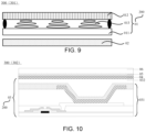
- FIG. 9 schematically illustrates a case where the display panel is the liquid crystal display panel 01
- FIG. 10 schematically illustrates a case where the display panel is the electroluminescent display panel 03 or the photoluminescent display panel 03.
- a main structure of the liquid crystal display panel 01 includes an array substrate 011, an opposite substrate 012 and a liquid crystal layer 013 disposed between the array substrate 011 and the opposite substrate 012.
- the array substrate 011 and the opposite substrate 012 are assembled together by a frame sealant, so that the liquid crystal layer 013 is within a region enclosed by the frame sealant.
- a main structure of the electroluminescent display panel 03 or the photoluminescent display panel 03 includes a display substrate 031 and an encapsulation layer 032 for encapsulating the display substrate 031.
- the encapsulation layer 032 may be an encapsulation film or an encapsulation substrate.
- some embodiments of the present disclosure provide an electronic apparatus 300, referring to FIGS. 9 and 10 , the electronic apparatus 300 includes the display device 200 as described in any of the above embodiments.
- the electronic apparatus 300 may be a display apparatus.
- the display apparatus may be any product or component with a display function, such as an AR helmet, AR glasses, a mobile phone, a tablet computer, a television, a display, a notebook computer, a digital photo frame, or a navigator.
- the display apparatus may be a liquid crystal display (LCD) apparatus 301.
- the display apparatus may be an electroluminescent display apparatus 302 or a photoluminescent display apparatus 302.
- the electroluminescent display apparatus may be an organic light-emitting diode (OLED) display apparatus, a quantum dot light-emitting diode (QLED) display apparatus or a small-sized light-emitting diode (e.g., Mini-LED or Micro-LED) display apparatus.
- the photoluminescent display apparatus may be a quantum dot photoluminescent display apparatus.
- the display apparatus is the liquid crystal display apparatus 301
- the display apparatus includes the liquid crystal display panel 01 and a backlight module 02.
- the backlight module is used for providing a light source for the liquid crystal panel 01, so that the liquid crystal panel 01 may normally display images.
- the display apparatus is the electroluminescence display apparatus 302 or the photoluminescence display apparatus 302, in some examples, as shown in FIG. 10 , the display apparatus includes the electroluminescent display panel 03 or the photoluminescent display panel 03, a polarizer 04, a first optically clear adhesive (OCA) 05 and a cover glass 02 that are arranged in sequence.
- OCA optically clear adhesive
- the electronic device and the electronic apparatus provided in the embodiments of the present disclosure each include the substrate 1 in any of the above embodiments. Therefore, the electronic device and the electronic apparatus have all the beneficial effects of the substrate 1, and it will not be repeated here.
- a thickness of the substrate 1 is relatively large due to structural strength requirements of the apparatus.
- energy required by the laser light for cutting the substrate is relatively high, and light spots are relatively large. Therefore, it is necessary to set a large second limit value d to prevent the laser light from being reflected to the inside of the substrate 1 through an edge of the substrate when the laser light cuts to the edge of the substrate, so as to prevent the laser light from being reflected back and forth inside the substrate 1 and avoid product defects.
- the second limit value may be in a range of 0.1 mm to 0.3 mm, inclusive.
- the second limit value may be set to increase with an area of the display region of the display apparatus.
- some embodiments of the present disclosure provide a method for cutting a substrate.
- the cutting method includes steps 101 to 103 (S101 to S103).
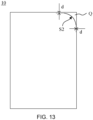
- step 101 a substrate motherboard 100 is cut into a plurality of substrates 10 whose corners are to be removed along first cutting path(s) S1.
- the substrate motherboard 100 may be a motherboard formed by assembling an array substrate motherboard and an opposite substrate motherboard (e.g. the LCD panel 01 shown in FIG. 9 ); the substrate motherboard 100 may also be the array substrate motherboard or the opposite substrate motherboard. Of course, the substrate motherboard 100 may also be a self-luminous display substrate motherboard, or a substrate motherboard provided with electronic elements therein. This is not limited in the present disclosure.
- a cutter wheel is used to cut the substrate motherboard 100 along the first cutting paths S1, so that the plurality of substrates 10 whose corners are to be removed are obtained.
- the substrate 10 whose corner(s) are to be removed has at least one corner Q.
- the substrate 10 whose corner(s) are to be removed may have four corners Q to be removed.
- second cutting path(s) S2 are determined on the substrate 10 whose corner(s) are to be removed.
- a second cutting path S2 corresponds to the cutting section of the substrate 1 described in any of the above embodiments (e.g., the cutting section 121 shown in FIG. 1 , 2 , 3A , 3B , 4A , 4B , 5 , 6 or 7 ).
- the term "correspond" means that an orthographic projection of the second cutting path S2 on the plane where the substrate 1 is located overlaps with the orthographic projection of the cutting section 121 on the plane where the substrate 1 is located.
- gaps d exist between two end points of the second cutting path S2 and two edges respectively close thereto of the corner Q.
- step 103 the substrate 10 whose corner(s) are to be removed is cut along each second cutting path S2, and then the corner(s) Q to be removed of the substrate 10 are removed by physical force, so that the substrate 1 described in any of the above embodiments is obtained.
- laser light may be used to cut the substrate 10 whose corner(s) are to be removed along the second cutting path S2.
- the physical force may be gravity, or force exerted by an external object (such as a human hand or a mechanical device).
- breaking tracks of two breaking sections are closer to the predetermined track. That is, a corner portion that should be broken off is less likely to be remained on the breaking section, and a surface of the breaking section is less likely to have burrs thereon. As a result, cutting yield of the substrate is improved.
- FIG. 14 shows a display panel 010 to which the method for cutting the substrate may be directly applied.
- the display panel 010 has a display region A and a peripheral region S.
- FIG. 14 illustrates an example where the peripheral region S surrounds the display region A.
- the display region A is provided with a plurality of sub-pixels P therein.
- the peripheral region S is used for wiring, and gate driving circuit(s) may also be provided in the peripheral region S.
- sub-pixels P arranged in the display region A are described by taking an example in which the plurality of sub-pixels P are arranged in a matrix for convenience of description.
- sub-pixels P arranged in a line in a horizontal direction X are referred to as sub-pixels in a same row
- sub-pixels P arranged in a line in a vertical direction Y are referred to as sub-pixels in a same column.
- Sub-pixels in the same row may be connected to a gate line
- sub-pixels in the same column may be connected to a data line.
- the display panel When the display panel is cut, it may be cut along a second cutting path S2 to remove a corner Q according to the method for cutting the substrate described in any of the above embodiments.
- a corner Q may be better broken along the predetermined track. That is, a portion that should be broken off is less likely to be remained on a surface that is formed after the corner Q is removed, and the surface is less likely to have burrs thereon. As a result, cutting yield of the display panel is improved.
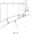
- the cut display panel further includes at least one metal wire K located in the display panel but at a periphery of the display panel.
- the metal wire K may be, for example, a grounding wire, an electromagnetic shielding wire, a gate line, or a data line.
- the metal wire K is disposed close to the cutting section, and there is no other wire between the metal wire K and the cutting section.
- any of points on the first circular arc R1 has a shortest distance to the metal wire K. By comparing shortest distances from the points on the first circular arc R1 to the metal wire K, a shortest distance D1 between the first circular arc R1 and the metal wire K may be obtained.
- the cutting section includes the second circular arc R2. Any of points on the second circular arc R2 has a shortest distance to the metal wire K. By comparing shortest distances from the points on the second circular arc R2 to the metal wire K, a shortest distance D2 between the second circular arc R2 and the metal wire K may be obtained.
- a positional relationship between the metal wire K and the cutting section is as follows: D1>D2. Since a position near a center of an end portion is relatively fragile and easy to be broken or cracked compared with other positions of the end portion, the cut display panel may obtain a relatively large "safety distance for electronic elements" in a region close to the center of the end portion with such a structural design. That is, in the region close to the center of the end portion, distances between the cutting section and the electronic elements of the display panel are relatively far, and thus it may reduce impact on the display function and service life of the display panel due to breaking of the end portion or crack(s) on the end portion, and improve reliability of the display panel.
- a shortest distance between the first straight line segment L1 and the metal wire K is D3.
- a positional relationship between the metal wire K and the cutting section is as follows: D1>D3.
- a shortest distance between the fourth circular arc R4 and the metal wire K is D4.
- a positional relationship between the metal wire K and the cutting section is as follows: D1>D4.
- shortest distances from the second circular arc R2, the first straight line segment L1 and the fourth circular arc R4 to the metal wire K are D2, D3, and D4, respectively.
- a positional relationship between the metal wire K and the cutting section is as follows: D1>max(D2,D3, D4), where max(D2, D3, D4) represents a maximum value in D2, D3, and D4.
- a shortest distance between the third circular arc R3 and the metal wire K is D2'.
- a positional relationship between the metal wire K and the cutting section is as follows: D1>D2'.
- a shortest distance between the second straight line segment L2 and the metal wire K is D3'.
- a positional relationship between the metal wire K and the cutting section is as follows: D1>D3'.
- a shortest distance between the fifth circular arc R5 and the metal wire K is D4'.
- a positional relationship between the metal wire K and the cutting section is as follows: D1>D4'.
- shortest distances from the third circular arc R3, the second straight line segment L2 and the fifth circular arc R5 to the metal wire K are D2', D3', D4' respectively.
- a positional relationship between the metal wire K and the cutting section is as follows: D1>max(D2',D3',D4'), where max(D2', D3', D4') represents a maximum value in D2', D3', and D4'.
- a panel structure given in the above examples enables the cut display panel to obtain a relatively large "safety distance for electronic elements" in the region close to the center of the end portion. That is, in the region close to the center of the end portion, distances between the cutting section and the electronic elements of the display panel are relatively far, and thus it may reduce impact on the display function and service life of the display panel due to the breaking of the end portion or the crack(s) on the end portion, and improve reliability of the display panel.
Landscapes
- Engineering & Computer Science (AREA)
- Physics & Mathematics (AREA)
- Optics & Photonics (AREA)
- Plasma & Fusion (AREA)
- Mechanical Engineering (AREA)
- Nonlinear Science (AREA)
- Chemical & Material Sciences (AREA)
- Crystallography & Structural Chemistry (AREA)
- Manufacturing & Machinery (AREA)
- General Physics & Mathematics (AREA)
- Processing Of Stones Or Stones Resemblance Materials (AREA)
- Structure Of Printed Boards (AREA)
- Dicing (AREA)
- Laser Beam Processing (AREA)
Description
- This application claims priority to
Chinese Patent Application No. 202010480020.9, filed on May 29, 2020 - Embodiments of the present disclosure relate to a substrate, and an electronic device.
- In a process of manufacturing a substrate, in the related art, a substrate motherboard is first cut into a plurality of separate substrates using a cutter wheel, and then a corner of the substrate is cut using laser light through an outer cutting process. The outer cutting process means that the laser light is used to directly cut the substrate from an edge of the substrate to another edge of the substrate, so that the corner of the substrate is cut off. However, since the substrate is provided with electronic elements therein, when the laser light cuts to the edge of the substrate, the edge of the substrate will refract the laser light to an inside of the substrate. As a result, the laser light is reflected back and forth inside the substrate. In this case, the laser light is easily reflected to the electronic elements of the substrate, which easily causes the electronic elements to be burned, resulting in product defects.
-
US 2020/070285 A1 provides an irregularly-shaped display panel and a cutting method. The display panel includes a display region and a non-display region surrounding the display region. The non-display region includes at least one irregularly-shaped boundary. The irregularly-shaped display panel further includes a substrate and the substrate includes a base substrate. The non-display region includes laser cutting trajectories. An orthographic projection of each of the laser cutting trajectories to the base substrate at least partially overlaps an orthographic projection of a corresponding irregularly-shaped boundary. Each of the laser cutting trajectories includes a cutting entry point and a cutting exit point at two ends thereof, and at least one of the cutting entry point and the cutting exit point does not overlap the orthographic projection of the corresponding irregularly-shaped boundary. -
US 2019/181387 A1 provides a display device. The display device includes first and second regions connected to each other. When viewed in a plan view, the first and second regions have a curved edge and a rectilinear edge, respectively. When viewed in a sectional view, a side surface of the first region may include a center region having a rectilinear shape and a side surface of the second region may include a center region having a curved shape. The side surface of the first region has a first roughness, and a side surface of the second region has a second roughness that is smoother than the first roughness. -
US 2019/369667 A1 provides a display device. The display device including a linear portion and a curved portion, includes a first substrate including a first surface and a second surface opposite the first surface; a second substrate including a third surface and a fourth surface opposite the third surface; and a display panel disposed between the first surface of the first substrate and the fourth surface of the second substrate. An outer surface adjacent to the first surface of the first substrate protrudes outward from an outer surface adjacent to the second surface of the first substrate, and a first width of a region of the first surface of the first substrate that does not overlap with the second surface in the linear portion is greater than a second width of a region of the first surface of the first substrate that does not overlap with the second surface of the first substrate in the curved portion. -
CN 111151894 A provides a special-shaped display panel and a cutting method thereof. The cutting method of the special-shaped display panel comprises the steps of providing a to-be-cut special-shaped display panel, cutting special-shaped corners and carrying out edge modification cutting, and glass residues at the arc ends of round corners can be removed to form smooth special-shaped corners. The special-shaped display panel is manufactured through the cutting method and comprises at least one special-shaped corner, and the special-shaped corner is formed by overlapping a first laser cutting track and a second laser cutting track. - In an aspect, the present disclosure provides a substrate which is defined by
claim 1. - In another aspect, the present disclosure provides an electronic device which is defined by claim 13.
- Further advantageous embodiments of the present disclosure are indicated in the dependent claims.
- In order to describe technical solutions in the present disclosure more clearly, accompanying drawings to be used in some embodiments of the present disclosure will be introduced briefly below. Obviously, the accompanying drawings to be described below are merely accompanying drawings of some embodiments of the present disclosure, and a person of ordinary skill in the art can obtain other drawings according to these accompanying drawings. In addition, the accompanying drawings to be described below may be regarded as schematic diagrams, and are not limitations on actual sizes of products, actual processes of methods and actual timings of signals involved in the embodiments of the present disclosure.
-
FIG. 1 is a structural diagram of a substrate, in accordance with some embodiments; -
FIG. 2 is a structural diagram of another substrate, in accordance with some embodiments; -
FIGS. 3A and3B are structural diagrams of yet another substrate, in accordance with some embodiments; -
FIGS. 4A and4B are structural diagrams of yet another substrate, in accordance with some embodiments; -
FIG. 5 is a structural diagram of yet another substrate, in accordance with some embodiments; -
FIG. 6 is a structural diagram of yet another substrate, in accordance with some embodiments; -
FIG. 7 is a structural diagram of yet another substrate, in accordance with some embodiments; -
FIG. 8 is a flow diagram of a method for cutting a substrate, in accordance with some embodiments; -
FIG. 9 is a structural diagram of a substrate motherboard, in accordance with some embodiments; -
FIG. 10 is a structural diagram of a substrate whose corner(s) are to be removed, in accordance with some embodiments; -
FIG. 11 is a structural diagram of an electronic device, in accordance with some embodiments; -
FIG. 12 is a structural diagram of an electronic apparatus, in accordance with some embodiments; -
FIG. 13 is a structural diagram of another electronic apparatus, in accordance with some embodiments; -
FIG. 14 is a structural diagram of a display panel, in accordance with some embodiments; and -
FIG. 15 is a structural diagram of another display panel, in accordance with some embodiments. - Technical solutions in some embodiments of the present disclosure will be described clearly and completely below with reference to the accompanying drawings. Obviously, the described embodiments are merely some but not all embodiments of the present disclosure.
- Unless the context requires otherwise, throughout the description and the claims, the term "comprise" and other forms thereof such as the third-person singular form "comprises" and the present participle form "comprising" are construed as an open and inclusive meaning, i.e., "including, but not limited to". In the description of the specification, the terms such as "one embodiment", "some embodiments", "exemplary embodiments", "example", "specific example" or "some examples" are intended to indicate that specific features, structures, materials or characteristics related to the embodiment(s) or example(s) are included in at least one embodiment or example of the present disclosure. Schematic representations of the above terms do not necessarily refer to the same embodiment(s) or example(s). In addition, the specific features, structures, materials or characteristics may be included in any one or more embodiments or examples in any suitable manner.
- Some embodiments of the present disclosure provide a
substrate 1. As shown inFIG. 1 , thesubstrate 1 includes at least twoedges 11 and at least oneend portion 12, and eachend portion 12 is connected to twoadjacent edges 11. It will be noted that,FIG. 1 only schematically illustrates oneend portion 12 of thesubstrate 1, and does not limit the number ofend portions 12 of thesubstrate 1. That is, in practical applications, thesubstrate 1 may be provided with only oneend portion 12, or two ormore end portions 12. Furthermore, in a case where thesubstrate 1 is provided with two ormore end portions 12, eachend portion 12 is connected to twoedges 11 adjacent thereto. For example, in a case where thesubstrate 1 includes four edges, and an end portion is provided between any two adjacent edges, the number of the end portions of thesubstrate 1 should be four. - As shown in
FIG. 1 , eachend portion 12 includes acutting section 121 and twobreaking section 122. An end of thecutting section 121 is connected to one of the twoadjacent edges 11 through abreaking section 122, another end of thecutting section 121 is connected to anotheredge 11 of the twoadjacent edges 11 through anotherbreaking section 122. - The
cutting section 121 is configured to be formed through cutting of a tool. For example, the tool may be a tool with a cutting function such as a laser cutting machine. Thecutting section 121 of thesubstrate 1 may be formed through cutting using laser light of the laser cutting machine. The breakingsections 122 are configured to be formed under an action of a physical force. For example, the physical force may be gravity or a pressure exerted by an external object. In a case where the physical force is the gravity, after thecutting section 121 is formed through cutting of the tool, a corner, which is to be removed, of a substrate will naturally be broken under the action of the gravity, and thus thesubstrate 1 is formed. In a case where the physical force is the pressure exerted by the external object, after thecutting section 121 is formed through cutting of the tool, a corner, which is to be removed, of a substrate will naturally be broken under the action of the pressure exerted by the external object (such as a human hand or a mechanical equipment), and thus thesubstrate 1 is formed. - In the embodiments, since the
end portion 12 of thesubstrate 1 includes both thecutting section 121 and the two breakingsections 122 located at both ends of thecutting section 121, when the corner, which is to be removed, of the substrate is removed, the laser light will not be directed toedges 11 of thesubstrate 1. As a result, the laser light will not be refracted to an inside of thesubstrate 1 through theedges 11 of thesubstrate 1, and in turn, the laser light will not be reflected back and forth inside thesubstrate 1, which may prevent the laser light from being reflected to electronic elements of thesubstrate 1. Therefore, it is beneficial to prevent the electronic elements from being burned, thereby reducing product defects. - In some embodiments, as shown in
FIG. 2 , an orthographic projection of thecutting section 121 on a plane where thesubstrate 1 is located includes a first circular arc R1, and an arc center O1 of the first circular arc R1 is located at an inside of thesubstrate 1. Therefore, a relatively regular rounded corner of thesubstrate 1 may be formed after a substrate whose corner is to be removed is cut and the corner to be removed of the substrate is broken, which may improve universality of thesubstrate 1. - It will be noted that, the orthographic projection of the
cutting section 121 on the plane where thesubstrate 1 is located may include only the first circular arc R1; or besides the first circular arc R1, the orthographic projection of thecutting section 121 on the plane where thesubstrate 1 is located further includes other portion(s) (e.g., as shown inFIGS. 3A ,3B ,4A ,4B andFIGS. 5 to 7 , including at least one of a second circular arc R2 and a third circular arc R3, and may further include a fourth circular arc R4, a fifth circular arc R5, a first straight line segment L1 and a second straight line segment L2). - In a case where the orthographic projection of the
cutting section 121 on the plane where thesubstrate 1 is located further includes other portion(s), a shortest distance between each point on the orthographic projection, on the plane where thesubstrate 1 is located, of thecutting section 121 and a circle where the first circular arc R1 is located is less than or equal to a first limit value. The first limit value may be related to a cutting accuracy of the substrate required by a product. For example, in a case where the cutting accuracy required by the product does not exceed h (that is, a cutting offset of thecutting section 121 does not exceed h), the first limit value may be set to be less than or equal to h. In addition, considering a positioning error of the cutting tool, the first limit value may be set to be approximately equal to 0.8h. For example, in a case where h is equal to 0.05 mm, the first limit value is approximately equal to 0.04 mm. Here, the expression "approximately equal to" refers to being within a range of plus or minus ten percent. That is, in the case where h is equal to 0.05 mm, the first limit value may be in a range of 0.036 mm to 0.044 mm, inclusive. In this case, it is easier to obtain thecutting section 121 that meets the cutting accuracy, and is beneficial to ameliorate a problem that thecutting section 121 is cut more or less. - In some embodiments, as shown in
FIG. 1 , a dimension of each breakingsection 122 in a first direction is a second limit value d. The first direction is a direction E parallel to the plane where thesubstrate 1 is located and perpendicular to anedge 111 that is connected to thebreaking section 1221, or a direction F parallel to the plane where thesubstrate 1 is located and perpendicular to anotheredge 112 that is connected to anotherbreaking section 1222. For a magnitude of the second limit value d, as long as it can satisfy that the breakingsections 122 may be formed under the action of the physical force after thecutting section 121 is formed through cutting. - For example, the second limit value d is in a range of 0.06 mm to 0.1 mm, inclusive. For example, the second limit value d may be in a range of 0.06 mm to 0.08 mm. In other words, a width of the
breaking section 1221 connected to theedge 111 in the first direction E may be 0.06 mm, 0.07 mm or 0.1 mm, etc. A width of the anotherbreaking section 1222 connected to theedge 112 in the second direction F may be 0.06 mm, 0.07 mm or 0.1 mm, etc. With such a design, after thecutting section 121 is formed by cutting the substrate whose corner is to be removed, the corner to be removed of the substrate is relatively easy to be broken, and undesired residual substances are not easily appeared on thesubstrate 1 obtained after the corner is broken. - Based on this, in order to make the
breaking section 122 be broken along a predetermined track, reduce the undesired residual substances generated on thebreaking section 122, and reduce burrs on a surface of thebreaking section 122, some embodiments of the present disclosure further modify thecutting section 121 of thesubstrate 1. For example, thecutting section 121 of thesubstrate 1 includes, but is not limited to, acutting section 121 in the following embodiments. - In the embodiments as claimed, as shown in
FIGS. 3A ,4A ,5 and6 , besides the first circular arc R1, the orthographic projection of thecutting section 121 on the plane where thesubstrate 1 is located further includes a second circular arc R2 and/or a third circular arc R3. - A first end of the second circular arc R2 is connected to an orthographic projection of a breaking section 122 (i.e., one of the two breaking
sections 122 included in theend portion 12 corresponding to the second circular arc R2) on the plane where thesubstrate 1 is located, and a second end of the second circular arc R2 is directly or indirectly connected to a first end of the first circular arc R1 (e.g.,FIG. 3A shows a case where the second end of the second circular arc R2 is directly connected to the first end of the first circular arc R1, andFIGS. 4A ,5 and6 show a case where the second end of the second circular arc R2 is indirectly connected to the first end of the first circular arc R1). An arc center of the second circular arc R2 is located at an outside of thesubstrate 1. With such a design, stress generated when the corner to be removed of the substrate is broken is uniformly distributed, and a phenomenon of stress concentration is less likely to occur. As a result, the corner may be better broken along the predetermined track, so that thebreaking section 122 of thesubstrate 1 is less likely to have residues and burrs thereon. - A first end of the third circular arc R3 is connected to an orthographic projection of another breaking section 122 (i.e., the other of the two breaking
sections 122 included in theend portion 12 corresponding to the third circular arc R3) on the plane where thesubstrate 1 is located, and a second end of the third circular arc R3 is directly or indirectly connected to a second end of the first circular arc R1 (e.g.,FIG. 3A shows a case where the second end of the third circular arc R3 is directly connected to the second end of the first circular arc R1, andFIGS. 4A ,5 and6 show a case where the second end of the third circular arc R3 is indirectly connected to the second end of the first circular arc R1). An arc center of the third circular arc R3 is located at the outside of thesubstrate 1. With such a design, the stress generated when the corner to be removed of the substrate is broken is uniformly distributed, and the phenomenon of stress concentration is less likely to occur. Therefore, the corner may be better broken along the predetermined track, so that thebreaking section 122 of thesubstrate 1 is less likely to have residues and burrs thereon. - In a case where the second end of the second circular arc R2 is directly connected to the first end of the first circular arc R1, and/or the second end of the third circular arc R3 is directly connected to the second end of the first circular arc R1.
- For any one of the second circular arc R2 and the third circular arc R3, in a design process, a position of the arc center O1 of the first circular arc R1 and a radius r1 of the first circular arc R1 are known. Referring to
FIG. 3B , a first auxiliary line m1 and a second auxiliary line m2 are firstly drawn on a side of any oneedge 11 close to the first circular arc R1. The first auxiliary line m1 is parallel to an orthographic projection of theedge 11 on the plane where thesubstrate 1 is located, and a distance between the first auxiliary line m1 and the orthographic projection of theedge 11 on the plane where thesubstrate 1 is located is the second limit value (e.g., the second limit value may be in the range of 0.06 mm to 0.1 mm, inclusive); the second auxiliary line m2 is parallel to the orthographic projection of theedge 11 on the plane where thesubstrate 1 is located, and a distance between the second auxiliary line m2 and the orthographic projection of theedge 11 on the plane where thesubstrate 1 is located is a sum of the second limit value and the first limit value (e.g., the first limit value may be in the range of 0.036 mm to 0.044 mm, inclusive). - Then, an intersection point is determined as a first position point T1, the intersection point being an intersection point closest to the first circular arc R1 in all intersection points of the circle where the first circular arc R1 is located and the second auxiliary line m2; and an intersection point is determined as a second position point T2, the intersection point being an intersection point closest to the first circular arc R1 in all intersection points of the circle where the first circular arc R1 is located and the first auxiliary line m1.
- Next, a third auxiliary line m3 passing through the first position point T1 is drawn, and an angle between the third auxiliary line m3 and the first auxiliary line m1 is a preset angle λ; the third auxiliary line m3 and the first auxiliary line m1 intersect at a third position point T3. A value of the preset angle λ is not limited in the embodiments, as long as it is ensured that the third position point T3 is between the first position point T1 and the second position point T2 in a direction parallel to the first auxiliary line m1. For example, the preset angle λ may be in a range of 30° to 60°, inclusive.
- Finally, a circular arc passing through the third position point T3 and tangent to both the third auxiliary line m3 and the first circular arc R1 is drawn, and the circular arc is the second circular arc R2 or the third circular arc R3.
- Based on this, for example, a radius of the second circular arc is r21, and/or a radius of the third circular arc is r21. r21 satisfies the following formula:

- k1 is in a range of 1 to 2, inclusive; r1 is the radius of the first circular arc R1; s is the first limit value; α is a central angle corresponding to an auxiliary circular arc, the auxiliary circular arc is obtained by extending the first circular arc R1, and distances from two opposite ends of the auxiliary circular arc to the two
edges 11 adjacent to the auxiliary circular arc are each equal to the second limit value. The first limit value and the second limit value have been described above, and will not be repeated here. - Referring to
FIG. 3B , in an example where the preset angle λ is equal to 45°. According to a geometric relationship, the radius r21 of the second circular arc R2 or the third circular arc R3 is equal to a length of a line segment T1T3 multiplied by tan ε1. A length of the line segment T1T3 is equal to
- In addition, according to a geometric relationship, it may be known that a length of a line segment O1N is r1•cos(45°-α/2)-s ;

- In addition, based on
FIG. 3B , it may be known that a tangent line passing through the first position point T1 and tangent to a circular arc to be determined (i.e., the second circular arc R2 or the third circular arc R3) almost coincides with a tangent line passing through the first position point T1 and tangent to the first circular arc R1. Therefore,

- It will be noted that the above derivation process is illustrated by considering an example in which the preset angle λ is equal to 45°. In the embodiments,

- Based on this, according to the obtained ε1, it may also be possible to calculate a central angle of the second circular arc R2 or the third circular arc R3. That is, the central angle of the second circular arc R2 or the third circular arc R3 is equal to (2 × (90° - ε1)).
- In the embodiments, the central angle of the second circular arc R2 may be in a range of 25° to 40°, inclusive; and the central angle of the third circular arc R3 may also be in the range of 25° to 40°, inclusive.
- In a case where the second end of the second circular arc R2 is indirectly connected to the first end of the first circular arc R1, and/or the second end of the third circular arc R3 is indirectly connected to the second end of the first circular arc R1.
- For example, as shown in
FIG. 4B , the orthographic projection of thecutting section 121 on the plane where the substrate is located further includes the first straight line segment L1 and/or the second straight line segment L2. - A first end of the first straight segment L1 is connected to the second end of the second circular arc R2, and a second end of the first straight segment L1 is connected to the first end of the first circular arc R1. With such a design, a smooth transition may be achieved between the first circular arc R1 and the second circular arc R2 through the first straight line segment L1, so that the
cutting section 121 is less likely to have sharp corners, which may better meet use requirements of the substrate. - A first end of the second straight line segment L2 is connected to the second end of the third circular arc R3, and a second end of the second straight line segment L2 is connected to the second end of the first circular arc R1. With such a design, a smooth transition may be achieved between the first circular arc R1 and the third circular arc R3 through the second straight line segment L2, so that the
cutting section 121 is less likely to have sharp corners, which may better meet use requirements of the substrate. - Based on this, as shown in
FIG. 4B , in some examples, the first straight line segment L1 is tangent to both the second circular arc R2 and the first circular arc R1, and/or the second straight line segment L2 is tangent to both the third circular arc R3 and the first circular arc R1. In this way, a smoother transition effect may be achieved between the first circular arc R1 and the second circular arc R2, and/or between the first circular arc R1 and the third circular arc R3. - In a design process, referring to
FIG. 4B , the position of the arc center O1 of the first circular arc R1 and the radius r1 of the first circular arc R1 are known. Referring toFIG. 4B , a fourth auxiliary line m4, a fifth auxiliary line m5 and a sixth auxiliary line m6 are firstly drawn on a side of any oneedge 11 close to thecutting section 121. The fourth auxiliary line m4 is parallel to an orthographic projection of theedge 11 on the plane where thesubstrate 1 is located, and a distance between the fourth auxiliary line m4 and the orthographic projection of theedge 11 on the plane where thesubstrate 1 is located is the second limit value (e.g., the second limit value may be in the range of 0.06 mm to 0.1 mm, inclusive); the fifth auxiliary line m5 is parallel to the orthographic projection of theedge 11 on the plane where thesubstrate 1 is located, and a distance between the fifth auxiliary line m5 and the orthographic projection of theedge 11 on the plane where thesubstrate 1 is located is the sum of the second limit value and the first limit value (e.g., the first limit value may be in the range of 0.036 mm to 0.044 mm, inclusive); the sixth auxiliary line m6 is parallel to the orthographic projection of theedge 11 on the plane where thesubstrate 1 is located, and a distance between the sixth auxiliary line m6 and the orthographic projection of theedge 11 on the plane where thesubstrate 1 is located is a sum of the second limit value, the first limit value and a third limit value. For example, the third limit value is approximately equal to 0.05 mm. Here, the term "approximately" means that the third limit value may be plus or minus ten percent on a basis of 0.05 mm. By setting the third limit value in this way, it is beneficial to achieve a smooth transition between the first straight line segment L1 (or the second straight line segment L2) subsequently formed and the circular arc adjacent to the first straight line segment L1 (or the second straight line segment L2). - Then, an intersection point is determined as a fourth position point T4, the intersection point being an intersection point closest to the first circular arc R1 in all intersection points of the circle where the first circular arc R1 is located and the fourth auxiliary line m4; an intersection point is determined as a fifth position point T5, the intersection point being an intersection point closest to the first circular arc R1 in all intersection points of the circle where the first circular arc R1 is located and the fifth auxiliary line m5; and an intersection point is determined as a sixth position point T6, the intersection point being an intersection point closest to the first circular arc R1 in all intersection points of the circle where the first circular arc R1 is located and the sixth auxiliary line m6.
- Next, a seventh auxiliary line m7 passing through the fifth position point T5 is drawn, and an angle between the seventh auxiliary line m7 and the fourth auxiliary line m4 is a preset angle λ; the seventh auxiliary line m7 and the fourth auxiliary line m4 intersect at a seventh position point T7. A value of the preset angle λ is not limited in the embodiments, as long as it is ensured that the seventh position point T7 is between the fourth position point T4 and the fifth position point T5 in a direction parallel to the fourth auxiliary line m4. For example, the preset angle λ may be in a range of 30° to 60°, inclusive.
- Finally, a circular arc (i.e., the second circular arc R2 or the third circular arc R3) passing through the seventh point T7 and tangent to both the seventh auxiliary line m7 and a line segment T5T6 is drawn. A portion of the line segment T5T6 between the drawn circular arc (i.e. the second circular arc R2 or the third circular arc R3) and the first circular arc R1 is the first straight line segment L1 or the second straight line segment L2.
- Based on this, for example, a radius of the second circular arc R2 is r22, and/or a radius of the third circular arc R3 is r22. r22 satisfies the following formula:

- k1 is in the range of 1 to 2, inclusive; r1 is the radius of the first circular arc R1; s is the first limit value; α is a central angle corresponding to an auxiliary circular arc, the auxiliary circular arc is obtained by extending the first circular arc R1, and distances from two opposite ends of the auxiliary circular arc to the two
edges 11 adjacent to the auxiliary circular arc are each equal to a second limit value; and u is the third limit value. The first limit value, the second limit value and the third limit value have been described above, and will not be repeated here. - Referring to
FIG. 4B , in an example where the preset angle λ is equal to 45°. According to a geometric relationship, the radius r22 of the second circular arc is equal to a length of a line segment T5T7 multiplied by tan ε2, and/or the radius r22 of the third circular arc is equal to the length of the line segment T5T7 multiplied by tan ε2. The length of the line segment T5T7 is equal to
- In addition, according to a geometric relationship, it may be known that a length of a line segment O1B1 is r1●cos(45°-α/2)-s, and a length of a line segment O1B2 is r1 ●cos(45°-α/2)-s-u.
- Based on this, according to the Pythagorean theorem, it may be known that:
a length of a line segment T5B1 is



- It will be noted that the above derivation process is illustrated by considering an example in which the preset angle λ is equal to 45°. In the embodiments,

- Based on this, according to the obtained ε2, it may also be possible to calculate a central angle of the second circular arc R2 or the third circular arc R3. That is, the central angle of the second circular arc R2 or the third circular arc R3 is equal to (2 × (90° - ε2)).
- In the embodiments, the central angle of the second circular arc R2 may be in a range of 30° to 40°, inclusive; and the central angle of the third circular arc R3 may also be in the range of 30° to 40°, inclusive.
- In the case where the second end of the second circular arc R2 is indirectly connected to the first end of the first circular arc R1, and/or the second end of the third circular arc R3 is indirectly connected to the second end of the first circular arc R1, in another example, as shown in
FIG. 5 , the orthographic projection of thecutting section 121 on the plane where the substrate is located further includes the fourth circular arc R4 and/or the fifth circular arc R5. - A first end of the fourth circular arc R4 is connected to the second end of the second circular arc R2, and a second end of the fourth circular arc R4 is connected to the first end of the first circular arc R1. With such a design, a smooth transition may be achieved between the first circular arc R1 and the second circular arc R2 through the fourth circular arc R4, so that the
cutting section 121 is less likely to have sharp corners, which may better meet use requirements of the substrate. - A first end of the fifth circular arc R5 is connected to the second end of the third circular arc R3, and a second end of the fifth circular arc R5 is connected to the second end of the first circular arc R1. With such a design, a smooth transition may be achieved between the first circular arc R1 and the third circular arc R3 through the fifth circular arc R5, so that the
cutting section 121 is less likely to have sharp corners, which may better meet the use requirements of the substrate. - In yet another example, as shown in
FIG. 6 , the orthographic projection of thecutting section 121 on the plane where the substrate is located further includes the first straight line segment L1 and the fourth circular arc R4; and/or the second straight line segment L2 and the fifth circular arc R5. - As shown in
FIG. 6 , a first end of the first straight line segment L1 is connected to the second end of the second circular arc R2, a second end of the first straight line segment L1 is connected to a first end of the fourth circular arc R4, and a second end of the fourth circular arc R4 is connected to the first end of the first circular arc R1. With such a design, a smooth transition may be achieved between the first circular arc R1 and the second circular arc R2 through the first straight line segment L1 and the fourth circular arc R4, so that thecutting section 121 is less likely to have sharp corners, which may better meet use requirements of the substrate. - As shown in
FIG. 6 , a first end of the second straight line segment L2 is connected to the second end of the third circular arc R3, a second end of the second straight line segment L2 is connected to a first end of the fifth circular arc R5, and a second end of the fifth circular arc R5 is connected to the second end of the first circular arc R1. With such a design, a smooth transition may be achieved between the first circular arc R1 and the third circular arc R3 through the second straight line segment L2 and the fifth circular arc R5, so that thecutting section 121 is less likely to have sharp corners, which may better meet use requirements of the substrate. - Based on this, in some examples, as shown in
FIG. 6 , the first straight line segment L1 is tangent to both the second circular arc R2 and the fourth circular arc R4, and/or the second straight line segment L2 is tangent to both the third circular arc R3 and the fifth circular arc R5. In this way, a smoother transition effect may be achieved between the second circular arc R2 and the fourth circular arc R4, and/or between the third circular arc R3 and the fifth circular arc R5; and thus, the transition effect between the first circular arc R1 and the second circular arc R2, and/or between the first circular arc R1 and the third circular arc R3 may be further enhanced. As a result, a probability of sharp corners occurring to thecutting section 121 is greatly reduced. - For solutions shown in
FIGS. 5 and6 , in a design process, referring toFIG. 7 , an eighth auxiliary line m8 is firstly drawn on a side of any oneedge 11 close to thecutting section 121, and the eighth auxiliary line m8 is parallel to an orthographic projection of theedge 11 on the plane where thesubstrate 1 is located, and a distance between the eighth auxiliary line m8 and the orthographic projection of theedge 11 on the plane where thesubstrate 1 is located is the second limit value as described above (e.g., the second limit value may be in the range of 0.06 mm to 0.1 mm). - Then, an intersection point is determined as an eighth position point T8, the intersection point being an intersection point closest to the first circular arc R1 in all intersection points of the circle where the first circular arc R1 is located and the eighth auxiliary line m8.
- Next, according to the radius r1 of the first circular arc R1 and the first limit value s, a radius r3 of an offset circular arc R0 is determined. The radius r3 of the offset circular arc R0 is equal to a difference between the radius r1 of the first circular arc R1 and the first limit value s (that is, r3 = r1 - s). Therefore, a position of the offset circular arc R0 may be determined. The offset circular arc R0 defines an allowable cutting offset of the product. An actual cutting position should not exceed the offset circular arc.
- A ninth auxiliary line m9 passing through the eighth position point T8 is drawn, and an angle between the ninth auxiliary line m9 and the eight auxiliary line m8 is a preset angle λ; the ninth auxiliary line m9 and the offset circular arc intersect at a ninth position point T9. A value of the preset angle λ is not limited in the embodiments, as long as it is ensured the ninth point T9 is closer to the first circular arc R1 than the eighth position point T8. For example, the preset angle λ may be in the range of 30° to 60°, inclusive.
- A tangent line of the offset arc R0 passing through the ninth position point T9 is drawn, and the tangent line intersects the circle where the first circular arc R1 is located at a tenth position point T10.
- Finally, a circular arc (i.e., the second circular arc R2 or the third circular arc R3) passing through the eight position point T8 and tangent to both the ninth auxiliary line m9 and a line segment T9T10 is drawn, an end of the circular arc opposite the eighth position point T8 is located on the line segment T9T10.
- Based on this, for a solution shown in
FIG. 5 , a circular arc (i.e., the fourth circular arc R4 in examples shown inFIG. 5 ) that is internally tangent to the first circular arc R1 and externally tangent to the second circular arc R2 is drawn between the second circular arc R2 and the first circular arc R1; and a circular arc (i.e., the fifth circular arc R5 in the examples shown inFIG. 5 ) that is internally tangent to the first circular arc R1 and externally tangent to the third circular arc R3 is drawn between the third circular arc R3 and the first circular arc R1. - For a solution shown in
FIG. 6 , as shown inFIG. 7 , an inverted circular is drawn at the tenth position point T10, so as to obtain a circular arc (i.e., the fourth circular arc R4 or the fifth circular arc R5) that is tangent to the line segment T9T10 and internally tangent to the first circular arc R1. In this case, a portion of the line segment T9T10 between the second circular arc R2 and the fourth circular arc R4 is the first straight line segment L1, and a portion of the line segment T9T10 between the third circular arc R3 and the fifth circular arc R5 is the second straight line segment L2. - For the solutions shown in
FIGS. 5 and6 , for example, the radius of the second circular arc R2 is r23, and/or the radius of the third circular arc R3 is r23. r23 satisfies the following formula:
- k1 is in the range of 1 to 2, inclusive; n is a minimum value of L in the formula

FIG. 7 ), the auxiliary circular arc is obtained by extending the first circular arc R1, and distances from two opposite ends of the auxiliary circular arc to the twoedges 11 adjacent to the auxiliary circular arc are each equal to the second limit value (as shown inFIG. 7 , a vertical distance between an end point T8 of the auxiliary circular arc R01 and anedge 11 is equal to the second limit value); r1 is the radius of the first circular arc R1, and s is the first limit value. The first limit value and the second limit value have been described above, and will not be repeated here. - In the design process, referring to
FIG. 7 , the radius of the second circular arc R2 is r23, and/or the radius of the third circular arc R3 is r23. For example, the preset angle λ is equal to 45°. According to a geometric relationship, r23 is equal to a length of a line segment T8T9 multiplied by tan ∠T8T9O2. - As shown in
FIG. 7 , β = 180° - λ - (45° + α/2), where α and λ are known quantities. Therefore, β = 90° - α/2. That is, β is also a known quantity. - The length of the line segment T8T9 is assumed to be L, and according to the cosine theorem, it will be known that


FIG. 7 , it will be noted that there are two intersection points between the ninth auxiliary line m9 and a circle where the offset circular arc is located. Therefore, two values of L may be calculated according to the above formula, and the length of the line segment T8T9 is a minimum value n of the two values of L. - Based on this, referring to
FIG. 7 , according to the cosine theorem, it may be known that, cos ε = (r3 2 + n2 - r1 2) / (2n·r3). Since the line segment T9T10 is the tangent of the offset circular arc R0, the line segment T9T10 and a line segment T9O1 (i.e. the radius of the offset circular arc) are perpendicular to each other. Therefore, ∠T8T9T10 = 360° - 90° - ε. That is, ∠T8T9T10 =
- Then, according to the trigonometric function, it may be obtained that,


- It will be noted that the above derivation process is illustrated by considering an example in which the preset angle λ is equal to 45°. In the embodiments,

- Based on this, according to the obtained ∠T8T9O2, a central angle of the second circular arc R2 or the third circular arc R3 may also be calculated. That is, the central angle of the second circular arc R2 or the third circular arc R3 is equal to (2 × (90° - ∠ T8T9O2)).
- In the embodiments, the central angle of the second circular arc R2 may be in the range of 30° to 40°, inclusive; and the central angle of the third circular arc R3 may also be in the range of 30° to 40°, inclusive.
- Based on the solutions shown in
FIGS. 5 and6 , for example, referring toFIG. 7 , a radius of the fourth circular arc R4 is r4, and/or a radius of the fifth circular arc R5 is r4. r4 =k2●r1, where k2 is in a range of 0.5 to 0.8, inclusive, and r1 is the radius of the first circular arc R1. With such a design, a smooth transition may be achieved between the first straight line segment L1 and the first circular arc R1, and/or between the second straight line segment L2 and the first circular arc R1, so that thecutting section 121 is less likely to have sharp corners. - A central angle of the fourth circular arc R4 may be in a range of 8° to 12°, inclusive; and a central angle of the fifth circular arc R5 may also be in the range of 8° to 12°, inclusive.
- In some embodiments, the radius of the first circular arc R1 is in a range of 7.01 mm to 8.74 mm, inclusive; the radius of the second circular arc R2 is in a range of 0.15 mm to 0.3mm, inclusive, and/or the radius of the third circular arc R3 is in the range of 0.15 mm to 0.3mm, inclusive; the radius of the fourth circular arc R4 is in a range of 5 mm to 6mm, inclusive, and/or the radius of the fifth circular arc R5 is in the range of 5 mm to 6mm, inclusive; the length of the first straight line segment L1 is in a range of 0.3mm to 0.52mm, inclusive, and/or the length of the second straight line segment L2 is in the range of 0.3mm to 0.52mm, inclusive. With such a design, the cutting section of the substrate formed by cutting is less likely to have sharp corners, which improves smoothness of the cutting section of the substrate.
- The first circular arc R1, the second circular arc R2, the third circular arc R3, the fourth circular arc R4, the fifth circular arc R5, the first straight line segment L1 and the second straight line segment L2 may be set in any one of the following manners.
- In a first manner, the radius of the first circular arc R1 is about 7.78 mm; the radius of the second circular arc R2 is about 0.3 mm, and/or the radius of the third circular arc R3 is about 0.3 mm; the radius of the fourth circular arc R4 is about 5 mm, and/or the radius of the fifth circular arc R5 is about 5 mm; the length of the first straight line segment L1 is about 0.3 mm, and/or the length of the second straight line segment L2 is about 0.3 mm. Here, the term "about" refers to, in practical applications, a deviation of plus or minus ten percent of each given value.
- In a second manner, the radius of the first circular arc R1 is about 7.93 mm; the radius of the second circular arc R2 is about 0.18 mm, and/or the radius of the third circular arc R3 is about 0.18 mm; the radius of the fourth circular arc R4 is about 6 mm, and/or the radius of the fifth circular arc R5 is about 6 mm; the length of the first straight line segment L1 is about 0.36 mm, and/or the length of the second straight line segment L2 is about 0.36 mm. Here, the term "about" refers to, in practical applications, a deviation of plus or minus ten percent of each given value.
- In a third manner, the radius of the first circular arc R1 is about 8.74 mm; the radius of the second circular arc R2 is about 0.24 mm, and/or the radius of the third circular arc R3 is about 0.24 mm; the radius of the fourth circular arc R4 is about 6 mm, and/or the radius of the fifth circular arc R5 is about 6 mm; the length of the first straight line segment L1 is about 0.44 mm, and/or the length of the second straight line segment L2 is about 0.44 mm. Here, the term "about" refers to, in practical applications, a deviation of plus or minus ten percent of each given value.
- In a fourth manner, the radius of the first circular arc R1 is about 7.41 mm; the radius of the second circular arc R2 is about 0.19 mm, and/or the radius of the third circular arc R3 is about 0.19 mm; the radius of the fourth circular arc R4 is about 5.5 mm, and/or the radius of the fifth circular arc R5 is about 5.5 mm; the length of the first straight line segment L1 is about 0.52 mm, and/or the length of the second straight line segment L2 is about 0.52 mm. Here, the term "about" refers to, in practical applications, a deviation of plus or minus ten percent of each given value.
- In a fifth manner, the radius of the first circular arc R1 is about 7.01 mm; the radius of the second circular arc R2 is about 0.15 mm, and/or the radius of the third circular arc R3 is about 0.15 mm; the radius of the fourth circular arc R4 is about 5 mm, and/or the radius of the fifth circular arc R5 is about 5 mm; the length of the first straight line segment L1 is about 0.48 mm, and/or the length of the second straight line segment L2 is about 0.48 mm. Here, the term "about" refers to, in practical applications, a deviation of plus or minus ten percent of each given value.
- Through the first manner to the fifth manner, widths of both ends of the corner to be removed of the substrate (i.e., widths of portions of the corner corresponding to the second circular arc R2 and the third circular arc R3) are relatively large, so that the stress distribution of the corner is relatively uniform when the corner is broken. Therefore, the phenomenon of stress concentration is less likely to occur. As a result, the corner may be better broken along the predetermined track, so that the breaking sections of the
substrate 1 are less likely to have residues and burrs thereon. - In another aspect, some embodiments of the present disclosure provide an
electronic device 200. As shown inFIG. 8 , theelectronic device 200 includes the substrate described in any of the above embodiments. Thesubstrate 1 is provided withelectronic elements 201 therein. Theelectronic element 201 may be, for example, a thin film transistor or a capacitor, or may be an electrode or an electronic circuit. Alternatively, theelectronic element 201 may be a combination of two or more of various electronic elements or structures. - The
electronic device 200 may be any of a display panel, a touch panel, a micro-fluidic chip or an electronic chip, which is not limited in the embodiments of the present disclosure. - In a case where the
electronic device 200 is the display panel, the display panel may be a liquid crystal display panel, an electroluminescent display panel or a photoluminescent display panel. For example,FIG. 9 schematically illustrates a case where the display panel is the liquidcrystal display panel 01; andFIG. 10 schematically illustrates a case where the display panel is theelectroluminescent display panel 03 or thephotoluminescent display panel 03. - As shown in
FIG. 9 , in the case where the display panel is the liquidcrystal display panel 01, a main structure of the liquidcrystal display panel 01 includes anarray substrate 011, anopposite substrate 012 and aliquid crystal layer 013 disposed between thearray substrate 011 and theopposite substrate 012. Thearray substrate 011 and theopposite substrate 012 are assembled together by a frame sealant, so that theliquid crystal layer 013 is within a region enclosed by the frame sealant. - As shown in
FIG. 10 , in the case where the display panel is theelectroluminescent display panel 03 or thephotoluminescent display panel 03, a main structure of theelectroluminescent display panel 03 or thephotoluminescent display panel 03 includes adisplay substrate 031 and anencapsulation layer 032 for encapsulating thedisplay substrate 031. Here, theencapsulation layer 032 may be an encapsulation film or an encapsulation substrate. - In yet another aspect, some embodiments of the present disclosure provide an
electronic apparatus 300, referring toFIGS. 9 and 10 , theelectronic apparatus 300 includes thedisplay device 200 as described in any of the above embodiments. - The
electronic apparatus 300 may be a display apparatus. The display apparatus may be any product or component with a display function, such as an AR helmet, AR glasses, a mobile phone, a tablet computer, a television, a display, a notebook computer, a digital photo frame, or a navigator. - As shown in
FIG. 9 , the display apparatus may be a liquid crystal display (LCD)apparatus 301. As shown inFIG. 10 , the display apparatus may be anelectroluminescent display apparatus 302 or aphotoluminescent display apparatus 302. In a case where the display apparatus is the electroluminescent display apparatus, the electroluminescent display apparatus may be an organic light-emitting diode (OLED) display apparatus, a quantum dot light-emitting diode (QLED) display apparatus or a small-sized light-emitting diode (e.g., Mini-LED or Micro-LED) display apparatus. In a case where the display apparatus is the photoluminescent display apparatus, the photoluminescent display apparatus may be a quantum dot photoluminescent display apparatus. - In the case where the display apparatus is the liquid
crystal display apparatus 301, in some examples, as shown inFIG. 9 , the display apparatus includes the liquidcrystal display panel 01 and abacklight module 02. The backlight module is used for providing a light source for theliquid crystal panel 01, so that theliquid crystal panel 01 may normally display images. - In the case where the display apparatus is the
electroluminescence display apparatus 302 or thephotoluminescence display apparatus 302, in some examples, as shown inFIG. 10 , the display apparatus includes theelectroluminescent display panel 03 or thephotoluminescent display panel 03, apolarizer 04, a first optically clear adhesive (OCA) 05 and acover glass 02 that are arranged in sequence. - The electronic device and the electronic apparatus provided in the embodiments of the present disclosure each include the
substrate 1 in any of the above embodiments. Therefore, the electronic device and the electronic apparatus have all the beneficial effects of thesubstrate 1, and it will not be repeated here. - In particular, in a case where the display apparatus is the television or a display apparatus with a relatively large display region (e.g., a dimension of the display region is greater than or equal to 10 inches), a thickness of the
substrate 1 is relatively large due to structural strength requirements of the apparatus. In this case, if laser light is used to cut the substrate, energy required by the laser light for cutting the substrate is relatively high, and light spots are relatively large. Therefore, it is necessary to set a large second limit value d to prevent the laser light from being reflected to the inside of thesubstrate 1 through an edge of the substrate when the laser light cuts to the edge of the substrate, so as to prevent the laser light from being reflected back and forth inside thesubstrate 1 and avoid product defects. For example, in the case where the display apparatus is the television or the display apparatus with the relatively large display region (e.g., the dimension of the display region is greater than or equal to 10 inches), the second limit value may be in a range of 0.1 mm to 0.3 mm, inclusive. For example, the second limit value may be set to increase with an area of the display region of the display apparatus. - In yet another aspect, some embodiments of the present disclosure provide a method for cutting a substrate.
- Referring to
FIG. 11 , the cutting method includessteps 101 to 103 (S101 to S103). - In
step 101, asubstrate motherboard 100 is cut into a plurality ofsubstrates 10 whose corners are to be removed along first cutting path(s) S1. - It will be noted that, the
substrate motherboard 100 may be a motherboard formed by assembling an array substrate motherboard and an opposite substrate motherboard (e.g. theLCD panel 01 shown inFIG. 9 ); thesubstrate motherboard 100 may also be the array substrate motherboard or the opposite substrate motherboard. Of course, thesubstrate motherboard 100 may also be a self-luminous display substrate motherboard, or a substrate motherboard provided with electronic elements therein. This is not limited in the present disclosure. In some examples, referring toFIG. 12 , a cutter wheel is used to cut thesubstrate motherboard 100 along the first cutting paths S1, so that the plurality ofsubstrates 10 whose corners are to be removed are obtained. - Referring to
FIG. 13 , for eachsubstrate 10 whose corner(s) are to be removed, thesubstrate 10 whose corner(s) are to be removed has at least one corner Q. For example, as shown inFIG. 13 , in a case where thesubstrate 10 whose corner(s) are to be removed has a rectangular shape, thesubstrate 10 whose corner(s) are to be removed may have four corners Q to be removed. - In
step 102, as shown inFIG. 13 , second cutting path(s) S2 are determined on thesubstrate 10 whose corner(s) are to be removed. A second cutting path S2 corresponds to the cutting section of thesubstrate 1 described in any of the above embodiments (e.g., thecutting section 121 shown inFIG. 1 ,2 ,3A ,3B ,4A ,4B ,5 ,6 or7 ). Here, the term "correspond" means that an orthographic projection of the second cutting path S2 on the plane where thesubstrate 1 is located overlaps with the orthographic projection of thecutting section 121 on the plane where thesubstrate 1 is located. - As shown in
FIG. 13 , gaps d exist between two end points of the second cutting path S2 and two edges respectively close thereto of the corner Q. - In
step 103, thesubstrate 10 whose corner(s) are to be removed is cut along each second cutting path S2, and then the corner(s) Q to be removed of thesubstrate 10 are removed by physical force, so that thesubstrate 1 described in any of the above embodiments is obtained. It will be noted that, in some examples, laser light may be used to cut thesubstrate 10 whose corner(s) are to be removed along the second cutting path S2. The physical force may be gravity, or force exerted by an external object (such as a human hand or a mechanical device). - With such a design, when the laser light is used to cut the corner Q to be removed of the
substrate 10 along the second cutting path S2, there are gaps d between the two end points of the second cutting path S2 and the two edges of the corner Q, so that the laser light will not be directed to the edges of thesubstrate 1, and the laser light will not be reflected to the inside of the substrate through the edges of thesubstrate 1. Therefore, the laser light will not be reflected back and forth inside thesubstrate 1, which may prevent the laser light from being reflected onto circuits in a peripheral region of thesubstrate 1. As a result, it is beneficial to prevent the circuits from being burned, which may reduce display defects of the product. - Moreover, in a case where the cutting section corresponding to the second cutting path S2 is the cutting section as shown in
FIG. 3A ,3B ,4A ,4B ,5 ,6 , or7 , in thesubstrate 1 formed by the cutting method, breaking tracks of two breaking sections are closer to the predetermined track. That is, a corner portion that should be broken off is less likely to be remained on the breaking section, and a surface of the breaking section is less likely to have burrs thereon. As a result, cutting yield of the substrate is improved. -
FIG. 14 shows adisplay panel 010 to which the method for cutting the substrate may be directly applied. As shown inFIG. 14 , thedisplay panel 010 has a display region A and a peripheral region S.FIG. 14 illustrates an example where the peripheral region S surrounds the display region A. The display region A is provided with a plurality of sub-pixels P therein. The peripheral region S is used for wiring, and gate driving circuit(s) may also be provided in the peripheral region S. - For the plurality of sub-pixels P disposed in the display region A, the embodiments of the present disclosure are described by taking an example in which the plurality of sub-pixels P are arranged in a matrix for convenience of description. In this case, sub-pixels P arranged in a line in a horizontal direction X are referred to as sub-pixels in a same row, and sub-pixels P arranged in a line in a vertical direction Y are referred to as sub-pixels in a same column. Sub-pixels in the same row may be connected to a gate line, and sub-pixels in the same column may be connected to a data line.
- When the display panel is cut, it may be cut along a second cutting path S2 to remove a corner Q according to the method for cutting the substrate described in any of the above embodiments. In this way, laser light will not be reflected back and forth inside the display panel, and the laser light may be prevented from being reflected onto the circuits in the peripheral region of the display panel, which is beneficial to preventing the circuits from being burned and further reducing display defects of the product. Moreover, the corner Q may be better broken along the predetermined track. That is, a portion that should be broken off is less likely to be remained on a surface that is formed after the corner Q is removed, and the surface is less likely to have burrs thereon. As a result, cutting yield of the display panel is improved.
- As shown in
FIG. 15 , the cut display panel further includes at least one metal wire K located in the display panel but at a periphery of the display panel. The metal wire K may be, for example, a grounding wire, an electromagnetic shielding wire, a gate line, or a data line. The metal wire K is disposed close to the cutting section, and there is no other wire between the metal wire K and the cutting section. - Any of points on the first circular arc R1 has a shortest distance to the metal wire K. By comparing shortest distances from the points on the first circular arc R1 to the metal wire K, a shortest distance D1 between the first circular arc R1 and the metal wire K may be obtained. In a case where the cut display panel has a structure as shown in
FIG. 3A , the cutting section includes the second circular arc R2. Any of points on the second circular arc R2 has a shortest distance to the metal wire K. By comparing shortest distances from the points on the second circular arc R2 to the metal wire K, a shortest distance D2 between the second circular arc R2 and the metal wire K may be obtained. A positional relationship between the metal wire K and the cutting section is as follows: D1>D2. Since a position near a center of an end portion is relatively fragile and easy to be broken or cracked compared with other positions of the end portion, the cut display panel may obtain a relatively large "safety distance for electronic elements" in a region close to the center of the end portion with such a structural design. That is, in the region close to the center of the end portion, distances between the cutting section and the electronic elements of the display panel are relatively far, and thus it may reduce impact on the display function and service life of the display panel due to breaking of the end portion or crack(s) on the end portion, and improve reliability of the display panel. - For example, in a case where the cutting section further includes the first straight line segment L1, similar to a definition of the shortest distance between the first circular arc R1 and the metal wire K, a shortest distance between the first straight line segment L1 and the metal wire K is D3. A positional relationship between the metal wire K and the cutting section is as follows: D1>D3.
- For example, in a case where the cutting section further includes the fourth circular arc R4, similar to the definition of the shortest distance between the first circular arc R1 and the metal wire K, a shortest distance between the fourth circular arc R4 and the metal wire K is D4. A positional relationship between the metal wire K and the cutting section is as follows: D1>D4.
- For example, as shown in
FIG. 15 , in a case where the cutting section includes the second circular arc R2, the first straight line segment L1, and the fourth circular arc R4, similar to the definition of the shortest distance between the first circular arc R1 and the metal wire K, shortest distances from the second circular arc R2, the first straight line segment L1 and the fourth circular arc R4 to the metal wire K are D2, D3, and D4, respectively. A positional relationship between the metal wire K and the cutting section is as follows: D1>max(D2,D3, D4), where max(D2, D3, D4) represents a maximum value in D2, D3, and D4. - For example, in a case where the cutting section includes the third circular arc R3, similar to the definition of the shortest distance between the first circular arc R1 and the metal wire K, a shortest distance between the third circular arc R3 and the metal wire K is D2'. A positional relationship between the metal wire K and the cutting section is as follows: D1>D2'.
- For example, in a case where the cutting section further includes the second straight line segment L2, similar to the definition of the shortest distance between the first circular arc R1 and the metal wire K, a shortest distance between the second straight line segment L2 and the metal wire K is D3'. A positional relationship between the metal wire K and the cutting section is as follows: D1>D3'.
- For example, in a case where the cutting section further includes the fifth circular arc R5, similar to the definition of the shortest distance between the first circular arc R1 and the metal wire K, a shortest distance between the fifth circular arc R5 and the metal wire K is D4'. A positional relationship between the metal wire K and the cutting section is as follows: D1>D4'.
- For example, in a case where the cutting section includes the third circular arc R3, the second straight line segment L2, and the fifth circular arc R5, similar to the definition of the shortest distance between the first circular arc R1 and the metal wire K, shortest distances from the third circular arc R3, the second straight line segment L2 and the fifth circular arc R5 to the metal wire K are D2', D3', D4' respectively. A positional relationship between the metal wire K and the cutting section is as follows: D1>max(D2',D3',D4'), where max(D2', D3', D4') represents a maximum value in D2', D3', and D4'.
- With such a structural design, based on a same principle, a panel structure given in the above examples enables the cut display panel to obtain a relatively large "safety distance for electronic elements" in the region close to the center of the end portion. That is, in the region close to the center of the end portion, distances between the cutting section and the electronic elements of the display panel are relatively far, and thus it may reduce impact on the display function and service life of the display panel due to the breaking of the end portion or the crack(s) on the end portion, and improve reliability of the display panel.
Claims (13)
- A substrate (1), comprising:at least two edges (11); and,at least one end portion (12), each end portion (12) being connected to two adjacent edges (11), whereinthe end portion (12) includes a cutting section (121) and two breaking sections (122); an end of the cutting section (121) is connected to one of the two adjacent edges (11) through a breaking section (122), and another end of the cutting section (121) is connected to another one of the two adjacent edges (11) through another breaking section (122);the cutting section (121) is configured to be formed through cutting of a tool, and the breaking sections (122) are configured to be formed under an action of a physical force;wherein an orthographic projection of the cutting section (121) on a plane where the substrate (1) is located includes:a first circular arc (R1), an arc center (O1) of the first circular arc (R1) being located at an inside of the substrate (1);whereinthe orthographic projection of the cutting section (121) on the plane where the substrate (1) is located further includes:at least one of a second circular arc (R2) and a third circular arc (R3), whereina first end of the second circular arc (R2) is connected to an orthographic projection of a breaking section (122) of the two breaking sections (122) on the plane where the substrate (1) is located, and a second end of the second circular arc (R2) is directly or indirectly connected to a first end of the first circular arc (R1); an arc center of the second circular arc (R2) is located at an outside of the substrate (1); anda first end of the third circular arc (R3) is connected to an orthographic projection of another breaking section (122) of the two breaking sections (122) on the plane where the substrate (1) is located, and a second end of the third circular arc (R3) is directly or indirectly connected to a second end of the first circular arc (R1); an arc center of the third circular arc (R3) is located at an outside of the substrate (1).
- The substrate (1) according to claim 1, wherein the at least one of the second circular arc (R2) and the third circular arc (R3) is directly connected to the first circular arc (R1), a radius of the second circular arc is r21, and/or a radius of the third circular arc is r21, and r21 satisfies a following formula:

- The substrate (1) according to claim 1, wherein the at least one of the second circular arc (R2) and the third circular arc (R3) is indirectly connected to the first circular arc (R1); andthe orthographic projection of the cutting section (121) on the plane where the substrate is located further includes at least one of a first straight line segment (L1) and a second straight line segment (L2), whereina first end of the first straight line segment (L1) is connected to the second end of the second circular arc (R2), and a second end of the first straight line segment (L1) is connected to the first end of the first circular arc (R1); anda first end of the second straight line segment (L2) is connected to the second end of the third circular arc (R3), and a second end of the second straight line segment (L2) is connected to the second end of the first circular arc (R1).
- The substrate (1) according to claim 3, wherein in a case where the orthographic projection of the cutting section (121) on the plane where the substrate (1) is located includes the second circular arc (R2) and the first straight line segment (L1), the first straight line segment (L1) is tangent to both the second circular arc (R2) and the first circular arc (R1); orin a case where the orthographic projection of the cutting section (121) on the plane where the substrate (1) is located includes the third circular arc (R3) and the second straight line segment (L2), the second straight line segment (L2) is tangent to both the third circular arc (R3) and the first circular arc (R1); orin a case where the orthographic projection of the cutting section (121) on the plane where the substrate (1) is located includes the second circular arc (R2), the third circular arc (R3), the first straight line segment (L1) and the second straight line segment (L2), the first straight line segment (L1) is tangent to both the second circular arc (R2) and the first circular arc (R1), and the second straight line segment (L2) is tangent to both the third circular arc (R3) and the first circular arc (R1).
- The substrate (1) according to claim 3 or 4, wherein a radius of the second circular arc is r22, and /or a radius of the third circular arc is r22, r22 satisfies a following formula:

- The substrate (1) according to claim 1, wherein the at least one of the second circular arc (R2) and the third circular arc (R3) is indirectly connected to the first circular arc (R1); andthe orthographic projection of the cutting section (121) on the plane where the substrate (1) is located further includes at least one of a fourth circular arc (R4) and a fifth circular arc (R5), whereina first end of the fourth circular arc (R4) is connected to the second end of the second circular arc (R2), and a second end of the fourth circular arc (R4) is connected to the first end of the first circular arc (R1); anda first end of the fifth circular arc (R5) is connected to the second end of the third circular arc (R3), and a second end of the fifth circular arc (R5) is connected to the second end of the first circular arc (R1).
- The substrate (1) according to claim 6, wherein in a case where the orthographic projection of the cutting section (121) on the plane where the substrate (1) is located includes the second circular arc (R2) and the fourth circular arc (R4), the fourth circular arc (R4) is internally tangent to the first circular arc (R1), and the fourth circular arc (R4) is externally tangent to the second circular arc (R2); orin a case where the orthographic projection of the cutting section (121) on the plane where the substrate (1) is located includes the third circular arc (R3) and the fifth circular arc (R5), the fifth circular arc (R5) is internally tangent to the first circular arc (R1), and the fifth circular arc (R5) is externally tangent to the third circular arc (R3); orin a case where the orthographic projection of the cutting section (121) on the plane where the substrate (1) is located includes the second circular arc (R2), the third circular arc (R3), the fourth circular arc (R4) and the fifth circular arc (R5), the fourth circular arc (R4) is internally tangent to the first circular arc (R1), the fourth circular arc (R4) is externally tangent to the second circular arc (R2), the fifth circular arc (R5) is internally tangent to the first circular arc (R1), and the fifth circular arc (R5) is externally tangent to the third circular arc (R3).
- The substrate (1) according to claim 1, wherein the at least one of the second circular arc (R2) and the third circular arc (R3) is indirectly connected to the first circular arc (R1);the orthographic projection of the cutting section (121) on the plane where the substrate (1) is located further includes at least one of a group consisting of a first straight line segment (L1) and a fourth circular arc (R4) and another group consisting of a second straight line segment (L2) and a fifth circular arc (R5), whereina first end of the first straight line segment (L1) is connected to the second end of the second circular arc (R2), a second end of the first straight line segment (L1) is connected to a first end of the fourth circular arc (R4), and a second end of the fourth circular arc (R4) is connected to the first end of the first circular arc (R1); anda first end of the second straight line segment (L2) is connected to the second end of the third circular arc (R3), and a second end of the second straight line segment (L2) is connected to a first end of the fifth circular arc (R5), a second end of the fifth circular arc (R5) is connected to the second end of the first circular arc (R1).
- The substrate (1) according to claim 8, wherein in a case where the orthographic projection of the cutting section (121) on the plane where the substrate (1) is located includes the second circular arc (R2), the fourth circular arc (R4) and the first straight line segment (L1), the first straight line segment (L1) is tangent to both the second circular arc (R2) and the fourth circular arc (R4), and the fourth circular arc (R4) is internally tangent to the first circular arc (R1); orin a case where the orthographic projection of the cutting section (121) on the plane where the substrate (1) is located includes the third circular arc (R3), the fifth circular arc (R5) and the second straight line segment (L2), the second straight line segment (L2) is tangent to both the third circular arc (R3) and the fifth circular arc (R5), and the fifth circular arc (R5) is internally tangent to the first circular arc (R1); orin a case where the orthographic projection of the cutting section (121) on the plane where the substrate (1) is located includes the second circular arc (R2), the third circular arc (R3), the fourth circular arc (R4), the fifth circular arc (R5), the first straight line segment (L1) and the second straight line segment (L2), the first straight line segment (L1) is tangent to both the second circular arc (R2) and the fourth circular arc (R4), the fourth circular arc (R4) is internally tangent to the first circular arc (R1), the second straight line segment (L2) is tangent to both the third circular arc (R3) and the fifth circular arc (R5), and the fifth circular arc (R5) is internally tangent to the first circular arc (R1).
- The substrate (1) according to any one of claims 6 to 9, wherein a radius of the second circular arc is r23, and /or a radius of the third circular arc is r23, r23 satisfies a following formula:


- The substrate (1) according to any one of claims 6 to 10, wherein a radius of the fourth circular arc is r4, and/or the fifth circular arc is r4, r4 =k2 · r1 ; where k2 is in a range of 0.5 to 0.8, inclusive; and r1 is a radius of the first circular arc (R1).
- The substrate (1) according to any one of claims 1 to 11, wherein a shortest distance between each point on the orthographic projection, on the plane where the substrate (1) is located, of the cutting section (121) and a circle where the first circular arc (R1) is located is less than or equal to a first limit value; and
a dimension of a breaking section (1221) of the two breaking sections (122) in a first direction is a second limit value, and the first direction is a direction (E) parallel to the plane where the substrate (1) is located and perpendicular to an edge (111) of the two adjacent edges (11) that is connected to the breaking section (1221); and/or a dimension of another breaking section (1222) of the two breaking sections (122) in a second direction is a second limit value, and the second direction is a direction (F) parallel to the plane where the substrate (1) is located and perpendicular to another edge (112) of the two adjacent edges (11) that is connected to the another breaking section (1222). - An electronic device (200), characterized by comprising:
at least one substrate (1) according to any one of claims 1 to 12.
Applications Claiming Priority (2)
| Application Number | Priority Date | Filing Date | Title |
|---|---|---|---|
| CN202010480020.9A CN113751889B (en) | 2020-05-29 | 2020-05-29 | Substrate and cutting method thereof, electronic device and electronic equipment |
| PCT/CN2021/086832 WO2021238468A1 (en) | 2020-05-29 | 2021-04-13 | Substrate and method for cutting same, and electronic device and electronic apparatus |
Publications (3)
| Publication Number | Publication Date |
|---|---|
| EP4160303A1 EP4160303A1 (en) | 2023-04-05 |
| EP4160303A4 EP4160303A4 (en) | 2023-12-20 |
| EP4160303B1 true EP4160303B1 (en) | 2025-02-12 |
Family
ID=78745525
Family Applications (1)
| Application Number | Title | Priority Date | Filing Date |
|---|---|---|---|
| EP21813346.0A Active EP4160303B1 (en) | 2020-05-29 | 2021-04-13 | Substrate and electronic device |
Country Status (4)
| Country | Link |
|---|---|
| US (1) | US12306483B2 (en) |
| EP (1) | EP4160303B1 (en) |
| CN (1) | CN113751889B (en) |
| WO (1) | WO2021238468A1 (en) |
Families Citing this family (1)
| Publication number | Priority date | Publication date | Assignee | Title |
|---|---|---|---|---|
| CN117600677A (en) * | 2023-12-04 | 2024-02-27 | 赣州市同兴达电子科技有限公司 | A kind of laser special-shaped cutting process for TFT liquid crystal display |
Family Cites Families (26)
| Publication number | Priority date | Publication date | Assignee | Title |
|---|---|---|---|---|
| JP5054496B2 (en) * | 2007-11-30 | 2012-10-24 | 浜松ホトニクス株式会社 | Processing object cutting method |
| JP2013505890A (en) | 2009-09-29 | 2013-02-21 | ピコドリル エスアー | Method and apparatus for cutting a substrate |
| KR101073563B1 (en) | 2010-02-08 | 2011-10-14 | 삼성모바일디스플레이주식회사 | Display device and manufacturing method thereof |
| EP2570225A1 (en) * | 2010-05-14 | 2013-03-20 | Asahi Glass Company, Limited | Cutting method and cutting device |
| JP2012061681A (en) * | 2010-09-15 | 2012-03-29 | Mitsuboshi Diamond Industrial Co Ltd | Laser cleaving apparatus |
| KR20120119082A (en) | 2011-04-20 | 2012-10-30 | 엘지디스플레이 주식회사 | Method of cutting substrate for liquid crystal display devece |
| TWI476063B (en) | 2011-10-04 | 2015-03-11 | Ind Tech Res Inst | Laser cutting method and apparatus |
| JP2013082589A (en) * | 2011-10-11 | 2013-05-09 | V Technology Co Ltd | Laser processing apparatus for glass substrate |
| CN102990230B (en) * | 2012-12-12 | 2015-08-12 | 京东方科技集团股份有限公司 | A kind of laser cutting machine |
| JP6441827B2 (en) * | 2013-03-07 | 2018-12-19 | スイッチ マテリアルズ インコーポレイテッドSwitch Materials Inc. | Sealed switchable film and method for sealing a switchable film |
| KR101999336B1 (en) * | 2013-04-09 | 2019-07-11 | 엘지디스플레이 주식회사 | Liquid crystal display, method of manufacturing the same |
| KR101521500B1 (en) * | 2013-11-15 | 2015-05-19 | 주식회사 에스에프에이 | Glass cutting system |
| US9260337B2 (en) * | 2014-01-09 | 2016-02-16 | Corning Incorporated | Methods and apparatus for free-shape cutting of flexible thin glass |
| CN104310779A (en) * | 2014-09-29 | 2015-01-28 | 合肥鑫晟光电科技有限公司 | Method for cutting base plate by laser and laser cutting equipment |
| JP6817822B2 (en) * | 2017-01-18 | 2021-01-20 | 株式会社ディスコ | Processing method |
| KR102607770B1 (en) * | 2017-12-08 | 2023-12-01 | 삼성디스플레이 주식회사 | Display panel and fabricating method of the same |
| KR102580292B1 (en) * | 2018-05-29 | 2023-09-19 | 삼성디스플레이 주식회사 | Display device, method for fabricating the device and laser processing apparatus for fabricating the device |
| CN109031743B (en) * | 2018-08-29 | 2021-07-09 | 厦门天马微电子有限公司 | Special-shaped display panel and cutting method thereof |
| CN109545937B (en) * | 2018-12-29 | 2024-07-30 | 佛山市国星半导体技术有限公司 | A high-brightness side-plated flip-chip LED chip and its manufacturing method |
| CN109702357A (en) | 2019-01-29 | 2019-05-03 | 大族激光科技产业集团股份有限公司 | A kind of laser processing disk method and system |
| CN110147003B (en) | 2019-05-16 | 2022-02-22 | Tcl华星光电技术有限公司 | Special-shaped display panel and manufacturing method thereof |
| CN110211973B (en) | 2019-06-12 | 2021-08-27 | 京东方科技集团股份有限公司 | Display panel and manufacturing method |
| CN110497101B (en) | 2019-08-26 | 2020-07-14 | 大连理工大学 | A kind of fiber laser cutting blade hole energy regulation method of metal sheet |
| CN110765609A (en) | 2019-10-18 | 2020-02-07 | 上海狮迈科技有限公司 | Offset compensation method for high-energy beam cutting path and high-energy beam cutting device |
| CN111151894A (en) * | 2020-01-03 | 2020-05-15 | 深圳市华星光电半导体显示技术有限公司 | Special-shaped display panel and cutting method thereof |
| CN212577823U (en) * | 2020-05-29 | 2021-02-23 | 京东方科技集团股份有限公司 | Substrate, electronic device, and electronic apparatus |
-
2020
- 2020-05-29 CN CN202010480020.9A patent/CN113751889B/en active Active
-
2021
- 2021-04-13 EP EP21813346.0A patent/EP4160303B1/en active Active
- 2021-04-13 WO PCT/CN2021/086832 patent/WO2021238468A1/en not_active Ceased
- 2021-04-13 US US17/780,053 patent/US12306483B2/en active Active
Also Published As
| Publication number | Publication date |
|---|---|
| CN113751889A (en) | 2021-12-07 |
| EP4160303A4 (en) | 2023-12-20 |
| CN113751889B (en) | 2025-05-06 |
| EP4160303A1 (en) | 2023-04-05 |
| WO2021238468A1 (en) | 2021-12-02 |
| US20220413325A1 (en) | 2022-12-29 |
| US12306483B2 (en) | 2025-05-20 |
Similar Documents
| Publication | Publication Date | Title |
|---|---|---|
| CN111384101B (en) | Flexible display device and electronic device including flexible display device | |
| JP5379817B2 (en) | Display panel | |
| CN113284423B (en) | Flexible display panel and display device | |
| US10770688B2 (en) | Display device | |
| US20240219773A1 (en) | Electronic device | |
| US12306483B2 (en) | Substrate and method for cutting the same, and electronic device and electronic apparatus | |
| CN116631297B (en) | Display device | |
| US20170320224A1 (en) | Display panel | |
| CN212577823U (en) | Substrate, electronic device, and electronic apparatus | |
| CN115224073A (en) | Display device | |
| KR101415805B1 (en) | Method for enhancing mechanical strength of glass | |
| US10451901B2 (en) | Display device on a substrate connected to another substrate with contact pads, vias, and conductive traces | |
| JP2007298747A (en) | Method for manufacturing display panel, and display panel | |
| CN111225512A (en) | Electronic device and method for manufacturing electronic device | |
| JP4731576B2 (en) | Display panel | |
| CN114063351A (en) | Sealing structure and electronic device with same | |
| JP2010085543A (en) | Display device and method for manufacturing the same | |
| JP2008052166A (en) | Manufacturing method of electrooptical device, electrooptical device, and electronic device | |
| CN116471873A (en) | Display panel, preparation method thereof and display device |
Legal Events
| Date | Code | Title | Description |
|---|---|---|---|
| STAA | Information on the status of an ep patent application or granted ep patent |
Free format text: STATUS: THE INTERNATIONAL PUBLICATION HAS BEEN MADE |
|
| PUAI | Public reference made under article 153(3) epc to a published international application that has entered the european phase |
Free format text: ORIGINAL CODE: 0009012 |
|
| STAA | Information on the status of an ep patent application or granted ep patent |
Free format text: STATUS: REQUEST FOR EXAMINATION WAS MADE |
|
| 17P | Request for examination filed |
Effective date: 20221228 |
|
| AK | Designated contracting states |
Kind code of ref document: A1 Designated state(s): AL AT BE BG CH CY CZ DE DK EE ES FI FR GB GR HR HU IE IS IT LI LT LU LV MC MK MT NL NO PL PT RO RS SE SI SK SM TR |
|
| DAV | Request for validation of the european patent (deleted) | ||
| DAX | Request for extension of the european patent (deleted) | ||
| REG | Reference to a national code |
Ref country code: DE Ref legal event code: R079 Free format text: PREVIOUS MAIN CLASS: G02F0001133300 Ipc: B23K0026380000 Ref document number: 602021026091 Country of ref document: DE |
|
| A4 | Supplementary search report drawn up and despatched |
Effective date: 20231116 |
|
| RIC1 | Information provided on ipc code assigned before grant |
Ipc: B23K 103/00 20060101ALN20231110BHEP Ipc: B23K 101/36 20060101ALN20231110BHEP Ipc: H04M 1/03 20060101ALN20231110BHEP Ipc: B32B 38/10 20060101ALN20231110BHEP Ipc: G02F 1/13 20060101ALN20231110BHEP Ipc: G02F 1/1333 20060101ALI20231110BHEP Ipc: B23K 26/38 20140101AFI20231110BHEP |
|
| RIC1 | Information provided on ipc code assigned before grant |
Ipc: B23K 103/00 20060101ALN20240626BHEP Ipc: B23K 101/36 20060101ALN20240626BHEP Ipc: H04M 1/03 20060101ALN20240626BHEP Ipc: B32B 38/10 20060101ALN20240626BHEP Ipc: G02F 1/13 20060101ALN20240626BHEP Ipc: G02F 1/1333 20060101ALI20240626BHEP Ipc: B23K 26/38 20140101AFI20240626BHEP |
|
| GRAP | Despatch of communication of intention to grant a patent |
Free format text: ORIGINAL CODE: EPIDOSNIGR1 |
|
| STAA | Information on the status of an ep patent application or granted ep patent |
Free format text: STATUS: GRANT OF PATENT IS INTENDED |
|
| RIC1 | Information provided on ipc code assigned before grant |
Ipc: B23K 103/00 20060101ALN20240724BHEP Ipc: B23K 101/36 20060101ALN20240724BHEP Ipc: H04M 1/03 20060101ALN20240724BHEP Ipc: B32B 38/10 20060101ALN20240724BHEP Ipc: G02F 1/13 20060101ALN20240724BHEP Ipc: G02F 1/1333 20060101ALI20240724BHEP Ipc: B23K 26/38 20140101AFI20240724BHEP |
|
| INTG | Intention to grant announced |
Effective date: 20240807 |
|
| GRAS | Grant fee paid |
Free format text: ORIGINAL CODE: EPIDOSNIGR3 |
|
| RAP3 | Party data changed (applicant data changed or rights of an application transferred) |
Owner name: BOE (HEBEI) MOBILE DISPLAY TECHNOLOGY CO., LTD. Owner name: BOE TECHNOLOGY GROUP CO., LTD. |
|
| GRAA | (expected) grant |
Free format text: ORIGINAL CODE: 0009210 |
|
| STAA | Information on the status of an ep patent application or granted ep patent |
Free format text: STATUS: THE PATENT HAS BEEN GRANTED |
|
| AK | Designated contracting states |
Kind code of ref document: B1 Designated state(s): AL AT BE BG CH CY CZ DE DK EE ES FI FR GB GR HR HU IE IS IT LI LT LU LV MC MK MT NL NO PL PT RO RS SE SI SK SM TR |
|
| REG | Reference to a national code |
Ref country code: GB Ref legal event code: FG4D |
|
| REG | Reference to a national code |
Ref country code: CH Ref legal event code: EP |
|
| REG | Reference to a national code |
Ref country code: DE Ref legal event code: R096 Ref document number: 602021026091 Country of ref document: DE |
|
| REG | Reference to a national code |
Ref country code: IE Ref legal event code: FG4D |
|
| REG | Reference to a national code |
Ref country code: NL Ref legal event code: MP Effective date: 20250212 |
|
| PG25 | Lapsed in a contracting state [announced via postgrant information from national office to epo] |
Ref country code: RS Free format text: LAPSE BECAUSE OF FAILURE TO SUBMIT A TRANSLATION OF THE DESCRIPTION OR TO PAY THE FEE WITHIN THE PRESCRIBED TIME-LIMIT Effective date: 20250512 |
|
| PG25 | Lapsed in a contracting state [announced via postgrant information from national office to epo] |
Ref country code: FI Free format text: LAPSE BECAUSE OF FAILURE TO SUBMIT A TRANSLATION OF THE DESCRIPTION OR TO PAY THE FEE WITHIN THE PRESCRIBED TIME-LIMIT Effective date: 20250212 |
|
| PG25 | Lapsed in a contracting state [announced via postgrant information from national office to epo] |
Ref country code: PL Free format text: LAPSE BECAUSE OF FAILURE TO SUBMIT A TRANSLATION OF THE DESCRIPTION OR TO PAY THE FEE WITHIN THE PRESCRIBED TIME-LIMIT Effective date: 20250212 |
|
| PGFP | Annual fee paid to national office [announced via postgrant information from national office to epo] |
Ref country code: DE Payment date: 20250424 Year of fee payment: 5 |
|
| PG25 | Lapsed in a contracting state [announced via postgrant information from national office to epo] |
Ref country code: ES Free format text: LAPSE BECAUSE OF FAILURE TO SUBMIT A TRANSLATION OF THE DESCRIPTION OR TO PAY THE FEE WITHIN THE PRESCRIBED TIME-LIMIT Effective date: 20250212 |
|
| REG | Reference to a national code |
Ref country code: LT Ref legal event code: MG9D |
|
| PG25 | Lapsed in a contracting state [announced via postgrant information from national office to epo] |
Ref country code: NO Free format text: LAPSE BECAUSE OF FAILURE TO SUBMIT A TRANSLATION OF THE DESCRIPTION OR TO PAY THE FEE WITHIN THE PRESCRIBED TIME-LIMIT Effective date: 20250512 Ref country code: IS Free format text: LAPSE BECAUSE OF FAILURE TO SUBMIT A TRANSLATION OF THE DESCRIPTION OR TO PAY THE FEE WITHIN THE PRESCRIBED TIME-LIMIT Effective date: 20250612 |
|
| PG25 | Lapsed in a contracting state [announced via postgrant information from national office to epo] |
Ref country code: NL Free format text: LAPSE BECAUSE OF FAILURE TO SUBMIT A TRANSLATION OF THE DESCRIPTION OR TO PAY THE FEE WITHIN THE PRESCRIBED TIME-LIMIT Effective date: 20250212 |
|
| PG25 | Lapsed in a contracting state [announced via postgrant information from national office to epo] |
Ref country code: HR Free format text: LAPSE BECAUSE OF FAILURE TO SUBMIT A TRANSLATION OF THE DESCRIPTION OR TO PAY THE FEE WITHIN THE PRESCRIBED TIME-LIMIT Effective date: 20250212 |
|
| PG25 | Lapsed in a contracting state [announced via postgrant information from national office to epo] |
Ref country code: PT Free format text: LAPSE BECAUSE OF FAILURE TO SUBMIT A TRANSLATION OF THE DESCRIPTION OR TO PAY THE FEE WITHIN THE PRESCRIBED TIME-LIMIT Effective date: 20250612 Ref country code: LV Free format text: LAPSE BECAUSE OF FAILURE TO SUBMIT A TRANSLATION OF THE DESCRIPTION OR TO PAY THE FEE WITHIN THE PRESCRIBED TIME-LIMIT Effective date: 20250212 |
|
| PG25 | Lapsed in a contracting state [announced via postgrant information from national office to epo] |
Ref country code: BG Free format text: LAPSE BECAUSE OF FAILURE TO SUBMIT A TRANSLATION OF THE DESCRIPTION OR TO PAY THE FEE WITHIN THE PRESCRIBED TIME-LIMIT Effective date: 20250212 Ref country code: GR Free format text: LAPSE BECAUSE OF FAILURE TO SUBMIT A TRANSLATION OF THE DESCRIPTION OR TO PAY THE FEE WITHIN THE PRESCRIBED TIME-LIMIT Effective date: 20250513 |
|
| REG | Reference to a national code |
Ref country code: AT Ref legal event code: MK05 Ref document number: 1765646 Country of ref document: AT Kind code of ref document: T Effective date: 20250212 |
|
| PG25 | Lapsed in a contracting state [announced via postgrant information from national office to epo] |
Ref country code: SE Free format text: LAPSE BECAUSE OF FAILURE TO SUBMIT A TRANSLATION OF THE DESCRIPTION OR TO PAY THE FEE WITHIN THE PRESCRIBED TIME-LIMIT Effective date: 20250212 |
|
| PG25 | Lapsed in a contracting state [announced via postgrant information from national office to epo] |
Ref country code: SM Free format text: LAPSE BECAUSE OF FAILURE TO SUBMIT A TRANSLATION OF THE DESCRIPTION OR TO PAY THE FEE WITHIN THE PRESCRIBED TIME-LIMIT Effective date: 20250212 |
|
| PG25 | Lapsed in a contracting state [announced via postgrant information from national office to epo] |
Ref country code: DK Free format text: LAPSE BECAUSE OF FAILURE TO SUBMIT A TRANSLATION OF THE DESCRIPTION OR TO PAY THE FEE WITHIN THE PRESCRIBED TIME-LIMIT Effective date: 20250212 |
|
| PG25 | Lapsed in a contracting state [announced via postgrant information from national office to epo] |
Ref country code: IT Free format text: LAPSE BECAUSE OF FAILURE TO SUBMIT A TRANSLATION OF THE DESCRIPTION OR TO PAY THE FEE WITHIN THE PRESCRIBED TIME-LIMIT Effective date: 20250212 |
|
| PG25 | Lapsed in a contracting state [announced via postgrant information from national office to epo] |
Ref country code: AT Free format text: LAPSE BECAUSE OF FAILURE TO SUBMIT A TRANSLATION OF THE DESCRIPTION OR TO PAY THE FEE WITHIN THE PRESCRIBED TIME-LIMIT Effective date: 20250212 |
|
| PG25 | Lapsed in a contracting state [announced via postgrant information from national office to epo] |
Ref country code: EE Free format text: LAPSE BECAUSE OF FAILURE TO SUBMIT A TRANSLATION OF THE DESCRIPTION OR TO PAY THE FEE WITHIN THE PRESCRIBED TIME-LIMIT Effective date: 20250212 Ref country code: CZ Free format text: LAPSE BECAUSE OF FAILURE TO SUBMIT A TRANSLATION OF THE DESCRIPTION OR TO PAY THE FEE WITHIN THE PRESCRIBED TIME-LIMIT Effective date: 20250212 |
|
| PG25 | Lapsed in a contracting state [announced via postgrant information from national office to epo] |
Ref country code: RO Free format text: LAPSE BECAUSE OF FAILURE TO SUBMIT A TRANSLATION OF THE DESCRIPTION OR TO PAY THE FEE WITHIN THE PRESCRIBED TIME-LIMIT Effective date: 20250212 |
|
| PG25 | Lapsed in a contracting state [announced via postgrant information from national office to epo] |
Ref country code: SK Free format text: LAPSE BECAUSE OF FAILURE TO SUBMIT A TRANSLATION OF THE DESCRIPTION OR TO PAY THE FEE WITHIN THE PRESCRIBED TIME-LIMIT Effective date: 20250212 |
|
| REG | Reference to a national code |
Ref country code: DE Ref legal event code: R097 Ref document number: 602021026091 Country of ref document: DE |
|
| REG | Reference to a national code |
Ref country code: CH Ref legal event code: H13 Free format text: ST27 STATUS EVENT CODE: U-0-0-H10-H13 (AS PROVIDED BY THE NATIONAL OFFICE) Effective date: 20251125 |
|
| PG25 | Lapsed in a contracting state [announced via postgrant information from national office to epo] |
Ref country code: LU Free format text: LAPSE BECAUSE OF NON-PAYMENT OF DUE FEES Effective date: 20250413 |
|
| PLBE | No opposition filed within time limit |
Free format text: ORIGINAL CODE: 0009261 |
|
| STAA | Information on the status of an ep patent application or granted ep patent |
Free format text: STATUS: NO OPPOSITION FILED WITHIN TIME LIMIT |
|
| PG25 | Lapsed in a contracting state [announced via postgrant information from national office to epo] |
Ref country code: MC Free format text: LAPSE BECAUSE OF FAILURE TO SUBMIT A TRANSLATION OF THE DESCRIPTION OR TO PAY THE FEE WITHIN THE PRESCRIBED TIME-LIMIT Effective date: 20250212 |
|
| REG | Reference to a national code |
Ref country code: BE Ref legal event code: MM Effective date: 20250430 |
|
| PG25 | Lapsed in a contracting state [announced via postgrant information from national office to epo] |
Ref country code: FR Free format text: LAPSE BECAUSE OF NON-PAYMENT OF DUE FEES Effective date: 20250430 |
|
| PG25 | Lapsed in a contracting state [announced via postgrant information from national office to epo] |
Ref country code: BE Free format text: LAPSE BECAUSE OF NON-PAYMENT OF DUE FEES Effective date: 20250430 |
|
| PG25 | Lapsed in a contracting state [announced via postgrant information from national office to epo] |
Ref country code: CH Free format text: LAPSE BECAUSE OF NON-PAYMENT OF DUE FEES Effective date: 20250430 |
|
| 26N | No opposition filed |
Effective date: 20251113 |
|
| PGFP | Annual fee paid to national office [announced via postgrant information from national office to epo] |
Ref country code: GB Payment date: 20260323 Year of fee payment: 6 |
|
| PG25 | Lapsed in a contracting state [announced via postgrant information from national office to epo] |
Ref country code: IE Free format text: LAPSE BECAUSE OF NON-PAYMENT OF DUE FEES Effective date: 20250413 |