EP4156512B1 - Differential signal amplification circuit, digital isolator, and receiver - Google Patents
Differential signal amplification circuit, digital isolator, and receiver Download PDFInfo
- Publication number
- EP4156512B1 EP4156512B1 EP21808054.7A EP21808054A EP4156512B1 EP 4156512 B1 EP4156512 B1 EP 4156512B1 EP 21808054 A EP21808054 A EP 21808054A EP 4156512 B1 EP4156512 B1 EP 4156512B1
- Authority
- EP
- European Patent Office
- Prior art keywords
- nmos transistor
- input terminal
- circuit
- common
- differential amplifier
- Prior art date
- Legal status (The legal status is an assumption and is not a legal conclusion. Google has not performed a legal analysis and makes no representation as to the accuracy of the status listed.)
- Active
Links
Images




Classifications
-
- H—ELECTRICITY
- H03—ELECTRONIC CIRCUITRY
- H03F—AMPLIFIERS
- H03F3/00—Amplifiers with only discharge tubes or only semiconductor devices as amplifying elements
- H03F3/45—Differential amplifiers
- H03F3/45071—Differential amplifiers with semiconductor devices only
- H03F3/45479—Differential amplifiers with semiconductor devices only characterised by the way of common mode signal rejection
-
- H—ELECTRICITY
- H03—ELECTRONIC CIRCUITRY
- H03F—AMPLIFIERS
- H03F1/00—Details of amplifiers with only discharge tubes, only semiconductor devices or only unspecified devices as amplifying elements
- H03F1/26—Modifications of amplifiers to reduce influence of noise generated by amplifying elements
-
- H—ELECTRICITY
- H03—ELECTRONIC CIRCUITRY
- H03F—AMPLIFIERS
- H03F3/00—Amplifiers with only discharge tubes or only semiconductor devices as amplifying elements
- H03F3/45—Differential amplifiers
- H03F3/45071—Differential amplifiers with semiconductor devices only
- H03F3/45076—Differential amplifiers with semiconductor devices only characterised by the way of implementation of the active amplifying circuit in the differential amplifier
- H03F3/45179—Differential amplifiers with semiconductor devices only characterised by the way of implementation of the active amplifying circuit in the differential amplifier using MOSFET transistors as the active amplifying circuit
- H03F3/45183—Long tailed pairs
-
- H—ELECTRICITY
- H03—ELECTRONIC CIRCUITRY
- H03F—AMPLIFIERS
- H03F3/00—Amplifiers with only discharge tubes or only semiconductor devices as amplifying elements
- H03F3/45—Differential amplifiers
- H03F3/45071—Differential amplifiers with semiconductor devices only
- H03F3/45479—Differential amplifiers with semiconductor devices only characterised by the way of common mode signal rejection
- H03F3/45632—Differential amplifiers with semiconductor devices only characterised by the way of common mode signal rejection in differential amplifiers with FET transistors as the active amplifying circuit
-
- H—ELECTRICITY
- H03—ELECTRONIC CIRCUITRY
- H03F—AMPLIFIERS
- H03F3/00—Amplifiers with only discharge tubes or only semiconductor devices as amplifying elements
- H03F3/45—Differential amplifiers
- H03F3/45071—Differential amplifiers with semiconductor devices only
- H03F3/45479—Differential amplifiers with semiconductor devices only characterised by the way of common mode signal rejection
- H03F3/45632—Differential amplifiers with semiconductor devices only characterised by the way of common mode signal rejection in differential amplifiers with FET transistors as the active amplifying circuit
- H03F3/45695—Differential amplifiers with semiconductor devices only characterised by the way of common mode signal rejection in differential amplifiers with FET transistors as the active amplifying circuit by using feedforward means
- H03F3/45699—Measuring at the input circuit of the differential amplifier
- H03F3/45708—Controlling the common source circuit of the differential amplifier
-
- H—ELECTRICITY
- H03—ELECTRONIC CIRCUITRY
- H03F—AMPLIFIERS
- H03F3/00—Amplifiers with only discharge tubes or only semiconductor devices as amplifying elements
- H03F3/45—Differential amplifiers
- H03F3/45071—Differential amplifiers with semiconductor devices only
- H03F3/45479—Differential amplifiers with semiconductor devices only characterised by the way of common mode signal rejection
- H03F3/45632—Differential amplifiers with semiconductor devices only characterised by the way of common mode signal rejection in differential amplifiers with FET transistors as the active amplifying circuit
- H03F3/45695—Differential amplifiers with semiconductor devices only characterised by the way of common mode signal rejection in differential amplifiers with FET transistors as the active amplifying circuit by using feedforward means
- H03F3/45699—Measuring at the input circuit of the differential amplifier
- H03F3/45717—Controlling the loading circuit of the differential amplifier
-
- H—ELECTRICITY
- H03—ELECTRONIC CIRCUITRY
- H03K—PULSE TECHNIQUE
- H03K19/00—Logic circuits, i.e. having at least two inputs acting on one output; Inverting circuits
- H03K19/003—Modifications for increasing the reliability for protection
- H03K19/00315—Modifications for increasing the reliability for protection in field-effect transistor circuits
-
- H—ELECTRICITY
- H03—ELECTRONIC CIRCUITRY
- H03K—PULSE TECHNIQUE
- H03K19/00—Logic circuits, i.e. having at least two inputs acting on one output; Inverting circuits
- H03K19/003—Modifications for increasing the reliability for protection
- H03K19/00346—Modifications for eliminating interference or parasitic voltages or currents
- H03K19/00361—Modifications for eliminating interference or parasitic voltages or currents in field effect transistor circuits
-
- H—ELECTRICITY
- H03—ELECTRONIC CIRCUITRY
- H03K—PULSE TECHNIQUE
- H03K19/00—Logic circuits, i.e. having at least two inputs acting on one output; Inverting circuits
- H03K19/0175—Coupling arrangements; Interface arrangements
- H03K19/017545—Coupling arrangements; Impedance matching circuits
-
- H—ELECTRICITY
- H03—ELECTRONIC CIRCUITRY
- H03K—PULSE TECHNIQUE
- H03K19/00—Logic circuits, i.e. having at least two inputs acting on one output; Inverting circuits
- H03K19/0175—Coupling arrangements; Interface arrangements
- H03K19/0185—Coupling arrangements; Interface arrangements using field effect transistors only
- H03K19/018557—Coupling arrangements; Impedance matching circuits
-
- H—ELECTRICITY
- H04—ELECTRIC COMMUNICATION TECHNIQUE
- H04B—TRANSMISSION
- H04B1/00—Details of transmission systems, not covered by a single one of groups H04B3/00 - H04B13/00; Details of transmission systems not characterised by the medium used for transmission
- H04B1/06—Receivers
- H04B1/10—Means associated with receiver for limiting or suppressing noise or interference
- H04B1/1027—Means associated with receiver for limiting or suppressing noise or interference assessing signal quality or detecting noise/interference for the received signal
-
- H—ELECTRICITY
- H04—ELECTRIC COMMUNICATION TECHNIQUE
- H04B—TRANSMISSION
- H04B1/00—Details of transmission systems, not covered by a single one of groups H04B3/00 - H04B13/00; Details of transmission systems not characterised by the medium used for transmission
- H04B1/38—Transceivers, i.e. devices in which transmitter and receiver form a structural unit and in which at least one part is used for functions of transmitting and receiving
- H04B1/40—Circuits
-
- H—ELECTRICITY
- H03—ELECTRONIC CIRCUITRY
- H03F—AMPLIFIERS
- H03F2200/00—Indexing scheme relating to amplifiers
- H03F2200/271—Indexing scheme relating to amplifiers the DC-isolation amplifier, e.g. chopper amplifier, modulation/demodulation amplifier, uses capacitive isolation means, e.g. capacitors
-
- H—ELECTRICITY
- H03—ELECTRONIC CIRCUITRY
- H03F—AMPLIFIERS
- H03F2200/00—Indexing scheme relating to amplifiers
- H03F2200/372—Noise reduction and elimination in amplifier
-
- H—ELECTRICITY
- H03—ELECTRONIC CIRCUITRY
- H03F—AMPLIFIERS
- H03F2200/00—Indexing scheme relating to amplifiers
- H03F2200/42—Indexing scheme relating to amplifiers the input to the amplifier being made by capacitive coupling means
-
- H—ELECTRICITY
- H03—ELECTRONIC CIRCUITRY
- H03F—AMPLIFIERS
- H03F2200/00—Indexing scheme relating to amplifiers
- H03F2200/48—Indexing scheme relating to amplifiers the output of the amplifier being coupled out by a capacitor
-
- H—ELECTRICITY
- H03—ELECTRONIC CIRCUITRY
- H03F—AMPLIFIERS
- H03F2203/00—Indexing scheme relating to amplifiers with only discharge tubes or only semiconductor devices as amplifying elements covered by H03F3/00
- H03F2203/45—Indexing scheme relating to differential amplifiers
- H03F2203/45051—Two or more differential amplifiers cascade coupled
-
- H—ELECTRICITY
- H03—ELECTRONIC CIRCUITRY
- H03F—AMPLIFIERS
- H03F2203/00—Indexing scheme relating to amplifiers with only discharge tubes or only semiconductor devices as amplifying elements covered by H03F3/00
- H03F2203/45—Indexing scheme relating to differential amplifiers
- H03F2203/45156—At least one capacitor being added at the input of a dif amp
-
- H—ELECTRICITY
- H03—ELECTRONIC CIRCUITRY
- H03F—AMPLIFIERS
- H03F2203/00—Indexing scheme relating to amplifiers with only discharge tubes or only semiconductor devices as amplifying elements covered by H03F3/00
- H03F2203/45—Indexing scheme relating to differential amplifiers
- H03F2203/45451—Indexing scheme relating to differential amplifiers the CSC comprising an addition circuit made by added current sources
-
- H—ELECTRICITY
- H03—ELECTRONIC CIRCUITRY
- H03F—AMPLIFIERS
- H03F2203/00—Indexing scheme relating to amplifiers with only discharge tubes or only semiconductor devices as amplifying elements covered by H03F3/00
- H03F2203/45—Indexing scheme relating to differential amplifiers
- H03F2203/45454—Indexing scheme relating to differential amplifiers the CSC comprising biasing means controlled by the input signal
-
- H—ELECTRICITY
- H03—ELECTRONIC CIRCUITRY
- H03F—AMPLIFIERS
- H03F2203/00—Indexing scheme relating to amplifiers with only discharge tubes or only semiconductor devices as amplifying elements covered by H03F3/00
- H03F2203/45—Indexing scheme relating to differential amplifiers
- H03F2203/45476—Indexing scheme relating to differential amplifiers the CSC comprising a mirror circuit
-
- H—ELECTRICITY
- H03—ELECTRONIC CIRCUITRY
- H03F—AMPLIFIERS
- H03F2203/00—Indexing scheme relating to amplifiers with only discharge tubes or only semiconductor devices as amplifying elements covered by H03F3/00
- H03F2203/45—Indexing scheme relating to differential amplifiers
- H03F2203/45544—Indexing scheme relating to differential amplifiers the IC comprising one or more capacitors, e.g. coupling capacitors
-
- H—ELECTRICITY
- H03—ELECTRONIC CIRCUITRY
- H03F—AMPLIFIERS
- H03F2203/00—Indexing scheme relating to amplifiers with only discharge tubes or only semiconductor devices as amplifying elements covered by H03F3/00
- H03F2203/45—Indexing scheme relating to differential amplifiers
- H03F2203/45596—Indexing scheme relating to differential amplifiers the IC comprising one or more biasing resistors
-
- H—ELECTRICITY
- H03—ELECTRONIC CIRCUITRY
- H03F—AMPLIFIERS
- H03F2203/00—Indexing scheme relating to amplifiers with only discharge tubes or only semiconductor devices as amplifying elements covered by H03F3/00
- H03F2203/45—Indexing scheme relating to differential amplifiers
- H03F2203/45631—Indexing scheme relating to differential amplifiers the LC comprising one or more capacitors, e.g. coupling capacitors
-
- H—ELECTRICITY
- H03—ELECTRONIC CIRCUITRY
- H03F—AMPLIFIERS
- H03F2203/00—Indexing scheme relating to amplifiers with only discharge tubes or only semiconductor devices as amplifying elements covered by H03F3/00
- H03F2203/45—Indexing scheme relating to differential amplifiers
- H03F2203/45702—Indexing scheme relating to differential amplifiers the LC comprising two resistors
-
- H—ELECTRICITY
- H04—ELECTRIC COMMUNICATION TECHNIQUE
- H04B—TRANSMISSION
- H04B1/00—Details of transmission systems, not covered by a single one of groups H04B3/00 - H04B13/00; Details of transmission systems not characterised by the medium used for transmission
- H04B1/06—Receivers
- H04B1/16—Circuits
Definitions
- the present invention relates to the field of electrical coupling apparatuses, and in particular, to a differential signal amplification circuit, a digital isolator, and a digital receiver.
- a digital isolation circuit is used to provide an intermediate circuit between a digital signal transmitting circuit and a digital signal receiving circuit.
- the isolation circuit enables communications between different electrical devices, such as communications between a weak-current circuit and a strong-current circuit, while preventing mutual interference between different circuits.
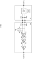
- Fig. 1 shows an implementation of a traditional digital isolator, which adopts an OOK modem technology and consists of a transmitting circuit TX and a receiving circuit RX. High and low levels in a digital signal are transmitted by sending and not sending a high-frequency clock signal.
- the transmitting circuit TX includes a digital signal input terminal TX_DATA, an oscillator OSC, and isolation capacitors Ciso1 and Ciso2.
- the receiving circuit RX includes isolation capacitors Ciso3 and Ciso4, two-stage amplification circuits AMP1 and AMP2, capacitors C3 and C4, a comparator CMP, and grounded resistors R1 and R2.
- the isolation capacitors Ciso1 and Cios3 as well as Cios2 and Cios4 are connected by wirings Wire1 and Wire2 respectively.
- CHANG IK ET AL "A GLOBAL OPERATIONAL AMPLIFIER WITHCONSTANT-GM INPUT AND OUTPUT STAGE", PROCEEDINGS OF IEEE TENCON'99, IEEE REGION 10 CONFERENCE, MULTIMEDIA TECHNOLOGY FOR ASIA-PACIFIC INFORMATIONINFRASTRUCTURE, THE SILLA CHEJU, CHEJU ISLAND, KOREASEPT.
- US5381113A1 involves a differential amplifier circuit utilizing a quadritail configuration.
- the object of the present invention is to solve the problem that an input voltage of the amplification circuit described above further results in abnormal signal transmission functions due to the direct-current offset voltages caused by common-mode interference.
- a differential signal amplification circuit is provided in accordance with appended independent apparatus claim 1.
- the common-mode transient adaptive biasing circuit comprises a common-mode detection circuit and an adaptive biasing circuit, wherein the common-mode detection circuit is connected to the positive input terminal and the negative input terminal of the primary differential amplifier respectively; and when the common-mode detection circuit detects the positive or negative common-mode transient interference signals at the positive input terminal and the negative input terminal, the adaptive biasing circuit is turned on to form a biasing current loop by the adaptive biasing circuit and the multi-stage differential amplifier.
- the common-mode detection circuit is configured to detect the positive common-mode transient interference signals, and comprises a first NMOS transistor MC1 and a second NMOS transistor MC2 that are connected in parallel, wherein gate electrodes of the first NMOS transistor MC1 and the NMOS transistor second MC2 are respectively connected to the positive input terminal and the negative input terminal of the primary differential amplifier; drain electrodes of the first NMOS transistor MC1 and the second NMOS transistor MC2 are connected to a biasing current output terminal of the multi-stage differential amplifier; and source electrodes of the first NMOS transistor MC1 and the second NMOS transistor MC2 are connected to a current input terminal of the adaptive biasing circuit.
- the adaptive biasing circuit comprises a third NMOS transistor MC3 and a fourth NMOS transistor MC4 having their source electrode and the drain electrode connected, wherein the drain electrode and the gate electrode of the third NMOS transistor MC3 are connected to an output terminal of the common-mode detection circuit; and the source electrode of the fourth NMOS transistor MC4 is connected to ground.
- the common-mode detection circuit is configured to detect the negative common-mode transient interference signals, and comprises:
- the adaptive biasing circuit is a current mirror in structure, and a mirroring current output terminal of the current mirror is connected to a biasing current output terminal of the multi-stage differential amplifier.
- the adaptive biasing circuit comprises a sixth NMOS transistor MD5 and a seventh NMOS transistor MD6 having their gate electrodes connected, wherein source electrodes of the sixth NMOS transistor MD5 and the seventh NMOS transistor MD6 are connected to ground; a drain electrode and a gate electrode of the sixth NMOS transistor MD5 are connected to a signal output terminal of the adaptive biasing circuit; and a drain electrode of the seventh NMOS transistor MD6 is connected to the biasing current output terminal of the multi-stage differential amplifier.
- the differential amplifier is a mirroring circuit, wherein the mirroring circuit comprises a third PMOS transistor MA3 and an eighth NMOS transistor MA1 whose drain electrodes are connected on one side,
- the differential amplifiers above the second stage comprises at least one stage of differential amplifier in which the source electrodes of the eighth NMOS transistor MA1 and the nineth NMOS transistor MA2 are connected to the biasing current output terminal.
- the positive input terminal and the negative input terminal of the primary differential amplifier are respectively connected with a third resistor R3 and a fourth resistor R4 to a level.
- the positive input terminal and the negative input terminal of the primary differential amplifier are connected to an isolation capacitor Ciso3 and an isolation capacitor Ciso4.
- a receiver for a digital isolator is provided.
- the present invention provides the receiver for the digital isolator including the differential signal amplification circuit, wherein the positive input terminal and the negative input terminal of the primary differential amplifier are connected to a positive input terminal and a negative input terminal of the digital isolator; the output terminal of the multi-stage differential amplifier is connected to an input terminal of a comparison circuit; and an output terminal of the comparison circuit is connected to an output terminal of the receiver for the digital isolator.
- a digital isolator includes a transmitter and a receiver
- the differential signal amplification circuit includes a multi-stage differential amplifier and a common-mode transient adaptive biasing circuit,
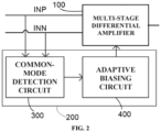
- Fig. 2 shows an architecture diagram of a differential signal amplification circuit, including a multi-stage differential amplifier 100 and a common-mode transient adaptive biasing circuit (CMTI) 200 for providing a biasing current of the multi-stage differential amplifier 100.
- CMTI common-mode transient adaptive biasing circuit
- the multi-stage differential amplifier 100 includes at least a two-stage differential amplifier.
- An input terminal of the common-mode transient adaptive biasing circuit 200 is connected to a positive input terminal INP and a negative input terminal INN of the multi-stage differential amplifier.
- a positive or negative common-mode interference signal generated on the input terminals is input into the common-mode transient adaptive biasing circuit 200.
- the common-mode transient adaptive biasing circuit 200 detects the positive or negative common-mode transient interference signals at the positive input terminal INP and the negative input terminal INN, determines that an effective positive or negative common-mode transient interference signal is detected after the common-mode transient interference signal reaches a starting voltage of the common-mode transient adaptive biasing circuit 200, and provides a biasing current of a differential amplifier of at least one stage above a second stage when the positive or negative common-mode transient interference signals are detected.
- the multi-stage amplification circuit inputs a direct-current offset voltage, and the offset voltage further becomes larger after amplified by a primary amplifier, resulting in the offset voltage being transferred along the multi-stage amplification circuit and eventually leading to abnormal signal transmission.
- the common-mode transient adaptive biasing circuit 200 is capable of compensating for amplifier output loss caused by the occurrence of the positive or negative common-mode transient interference signals.
- a primary offset voltage occurs, a positive or negative input voltage and a reverse input voltage of a primary amplification circuit are increased.
- the common-mode transient adaptive biasing circuit 200 When the voltages change to exceed a starting voltage of the common-mode transient adaptive biasing circuit, the common-mode transient adaptive biasing circuit 200 provides a current in a differential amplifier above the second stage by providing the biasing currents.
- the differential currents compensate for reduced output swing and gain loss of the differential amplifiers caused by voltage imbalance, and avoid continuous transfer of the direct-current input voltage mismatch caused by the common-mode signals between second-stage differential amplifiers or the differential amplifiers above the second stage. Therefore, the interference caused by the common-mode signals to signal transmission is suppressed.
- the common-mode transient adaptive biasing circuit 200 compensates for the differential amplifiers of each stage or unspecified number of stages above a second-stage amplification circuit.
- the multi-stage amplification circuit 100 includes a plurality of differential amplifiers AMP1 to AMPN having inputs and outputs connected in series.
- the positive input terminal INP and the negative input terminal INN of the primary differential amplifier AMP1 serve as input terminals of the multi-stage amplification circuit.
- a biasing current output terminal of any number of amplifiers in AMP2 to AMPN is connected to the common-mode transient adaptive biasing circuit 200.
- the common-mode transient adaptive biasing circuit adjusts the biasing currents of a plurality of differential amplifiers simultaneously.
- the differential amplifiers may be connected to the common-mode transient adaptive biasing circuit in the order of AMP2, AMP3, AMP4, AMPS ...
- the differential amplifiers may be connected to the common-mode transient adaptive biasing circuit every other stage in the order of AMP2, AMP4, AMP6, AMPS ... AMP2n or by any other electrical connection method known by those skilled in the art.
- the number of the common-mode transient adaptive biasing circuits 200 is not limited to one as shown in Fig. 3 , but may be multiple.
- a connection relationship between the common-mode transient adaptive biasing circuits 200 and the multi-stage differential amplifiers AMP1 to AMPN is one-to-one connection or one-to-many connection or many-to-one connection or many-to-many connection.
- the common-mode transient adaptive biasing circuits may provide compensation for the biasing currents of a one-stage or multi-stage differential amplifier simultaneously.
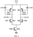
- Fig. 4 is a schematic structural diagram of the primary differential amplifier AMP1 in the multi-stage amplification circuit.
- a biasing current output terminal IBCMTI is added in Fig. 5 in addition to those shown in Fig. 4 .
- the differential amplifiers AMP1 to AMPN at least one stage of the differential amplifiers is provided with the biasing current output terminal IBCMTI shown in Fig. 5 .
- a differential amplification circuit is composed of a plurality of basic elements connected in a mirrored manner.
- the mirroring circuit includes a PMOS transistor MA3 and an NMOS transistor MA 1 with their drain electrodes connected in series on the left side.
- the source electrode of the PMOS transistor MA3 is connected to a power supply VCC
- a capacitor CA1 is connected between the gate electrode and the source electrode of the PMOS transistor MA3
- a biasing resistor RA1 is connected between the gate electrode and the drain electrode of the PMOS transistor.
- the drain electrode of the NMOS transistor MA1 is connected to a negative output terminal OUTN of the differential amplifier
- the gate electrode of the NMOS transistor MA1 is connected to the positive input terminal INP of the differential amplifier.
- the mirroring structure includes a PMOS transistor MA4 and an NMOS transistor MA2 with their drain electrodes connected in series on the right side.
- the source electrode of the PMOS transistor MA4 is connected to the power supply VCC
- a capacitor CA2 is connected between the gate electrode and the source electrode of the PMOS transistor MA4
- a biasing resistor RA2 is connected between the gate electrode and the drain electrode of the PMOS transistor MA4.
- the drain electrode of the NMOS transistor MA2 is connected to a positive output terminal OUTP of the differential amplifier
- the gate electrode of the NMOS transistor MA2 is connected to the negative input terminal INN of the differential amplifier.
- the source electrodes of the PMOS transistor MA3 and the PMOS transistor MA4 on both sides of the mirroring circuit are connected in parallel, the source electrodes of the NMOS transistor MA1 and the NMOS transistor MA2 on both sides of the mirroring circuit are connected in parallel, and the source electrodes of the NMOS transistor MA1 and the NMOS transistor MA2 are connected to the drain electrode of a grounded NMOS transistor MA5.
- the gate electrode of the grounded NMOS transistor MA5 is connected to a reference level VBN to provide a biasing current required by the amplifier during normal operation.
- the source electrode of the NMOS transistor MA1/MA2 is connected to the biasing current output terminal IBCMTI.
- the biasing currents are output, mirroring currents on both sides of the differential circuit are increased, and the difference in output potentials between the positive output terminal OUTP and the negative output terminal OUTN of the differential amplification circuit becomes larger. That is, the corresponding output signal waveform swing becomes larger.
- the amplifiers having at least one stage are provided with the biasing current output terminals IBCMTI.
- the biasing current output terminals IBCMTI at different stages are connected to the common-mode transient adaptive biasing circuit 200 to form multi-stage output gain and swing compensation.
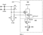
- Figs. 6 and 7 show two embodiments of the common-mode transient adaptive biasing circuit.
- the common-mode transient adaptive biasing circuit shown in Fig. 6 is configured to detect and suppress the positive common-mode transient interference signals.
- the common-mode transient adaptive biasing circuit shown in Fig. 7 is configured to detect and suppress the negative common-mode transient interference signals.
- positive and negative common-mode transient adaptive biasing circuits one of them may be used separately to be connected to the multi-stage differential amplifier 100, or both of them are connected in parallel and connected to the multi-stage differential amplifier 100 simultaneously for use.
- the common-mode transient adaptive biasing circuit 200 shown in Fig. 6 is connected to the input terminals of the primary amplifier.
- the positive input terminal INP and the negative input terminal INN of the primary amplifier AMP1 are connected to a positive input terminal RXINP and a negative input terminal RXINN of the receiver described below by isolation capacitors Ciso3 and Ciso4.
- the positive input terminal and the negative input terminal of the primary amplifier are connected to a level VCM by resistors R3 and R4.
- the adaptive biasing circuit detects the direct-current voltages Vi1 and Vi2, and determines whether common-mode interference occurs based on values of the direct-current voltages Vi1 and Vi2.
- the common-mode transient adaptive biasing circuit 200 includes a common-mode detection circuit 300 and an adaptive biasing circuit 400.
- the common-mode detection circuit 300 includes an NMOS transistor MC1 and an NMOS transistor MC2 that are connected in parallel.
- the gate electrodes of the two NMOS transistors, as the input terminals of the common-mode transient adaptive biasing circuit, are respectively connected to the positive input terminal INP and the negative input terminal INN of the primary differential amplifier.
- the drain electrode of the NMOS transistor MC1/MC2 is connected to the biasing current output terminal IBCMTI of the differential amplification circuit, and the source electrodes of the NMOS transistor MC1 and the NMOS transistor MC2 are connected to a current input terminal BiasIN of the adaptive biasing circuit.
- the adaptive biasing circuit 400 includes an NMOS transistor MC3 and an NMOS transistor MC4 having their source electrode and the drain electrode connected in series.
- the drain electrode and the gate electrode of the NMOS transistor MC3 are connected to an output terminal CMTIOUT of the common-mode detection circuit 300, and the source electrode of the NMOS transistor MC4 is connected to the ground.
- the gate electrode of the grounded NMOS transistor MC4 is connected to the reference level VBN for generating the biasing currents for compensating.
- the starting voltage of the common-mode transient adaptive biasing circuit is the sum of threshold voltages of the NMOS transistor MC1 or MC2 and the NMOS transistor MC3.
- the NMOS transistors of the common-mode detection circuit 300 are turned on, so that the adaptive biasing circuit 400 is communicated with the biasing current output terminal IBCMTI.
- the common-mode detection circuit 300 causes the adaptive biasing circuit 400 to form a biasing current loop with at least one of the differential amplifiers AMP2 ... AMPN.
- a biasing current is formed in the adaptive biasing current loop. The currents at the biasing current output terminal IBCMTI flow through the adaptive biasing circuit 400 to the ground.
- the biasing currents increase the currents of the mirroring circuit in the differential amplifier, so that the gain and output swing of the corresponding differential amplifier are increased, thereby compensating for output direct-current imbalance of the primary differential amplifier.
- the increase in output swing of the differential signal amplification circuit eliminates the influence of common-mode signal interference.
- the negative common-mode transient adaptive biasing circuit shown in Fig. 7 is connected to the input terminals of the primary amplification circuit, and it is connected to the positive common-mode transient adaptive biasing circuit 200 shown in Fig. 6 in parallel. Moreover, it is connected to the positive input terminal INP or the negative input terminal INN of the primary differential amplifier AMP1 as well as the resistor R1 or R2 in the same manner as that in which it is connected to the positive common-mode transient adaptive biasing circuit shown in Fig. 6 .
- the common-mode transient adaptive biasing circuit shown Fig. 7 includes a common-mode detection circuit 600 and an adaptive biasing circuit 800.
- the common mode detection circuit 600 includes a PMOS transistor MD4 and an NMOS transistor MD3 whose drain electrodes are connected in series are provided.
- the source electrode of the PMOS transistor MD4 is connected to the power supply VCC, and the gate electrodes of the PMOS transistor MD4 and the NMOS transistor MD3 are respectively connected to a level VBP and a level VSET.
- the common mode detection circuit 600 includes a PMOS transistor MD1 and a PMOS transistor MD2 connected in parallel having their source electrodes connected to the source electrode of the NMOS transistor MD3, the gate electrodes of the PMOS transistor MD1 and the PMOS transistor MD2 are respectively connected to the positive input terminal INP and the negative input terminal INN of the primary differential amplifier AMP1, and the drain electrodes of the PMOS transistor MD1 and the PMOS transistor MD2 are connected to a signal input terminal BiasIN' of the adaptive biasing circuit 800.
- the common-mode detection circuit 600 may detect the negative common-mode transient interference signals and adaptively adjust the biasing currents.
- the PMOS transistor MD4 generates a biasing current according to the level VBP
- the PMOS transistor MD1 and the PMOS transistor MD2 detect a common-mode voltage, and when VCM is less than VSET minus a threshold voltage of MD3 and a threshold voltage of MD1 or MD2 (i.e., VCM ⁇ VSET -
- a current signal output is generated at an output terminal CMTIOUT' of the common-mode detection circuit.
- the adaptive biasing circuit 800 is a current mirror in structure.
- a mirroring current output terminal of the current mirror is connected to the biasing current output terminal IBCMTI of the multi-stage differential amplifier 100.
- the adaptive biasing circuit includes an NMOS transistor MD5 and an NMOS transistor MD6 having their gate electrodes connected, and source electrodes of the NMOS transistor MD5 and the NMOS transistor MD6 are connected to the ground.
- the drain electrode and the gate electrode of the NMOS transistor MD5 are connected to the signal output terminal CMTIOUT' of the adaptive biasing circuit 800.
- the drain electrode of the NMOS transistor MD6 is connected to the biasing current output terminal IBCMTI of the multi-stage differential amplifier 100.
- a current signal passes through the gate electrodes of the NMOS transistor MD5 and NMOS transistor MD6 and forms a mirroring current at the drain electrode of the NMOS transistor MD6.
- the mirroring currents increase the currents of the mirroring circuit in the multi-stage differential amplifier 100, so that the gain and output swing of the corresponding differential amplifier are increased, eliminating the influence of common-mode signal interference.
- Fig. 8 shows a digital isolator including a transmitter TX and a receiver RX isolated by capacitors.
- the digital isolator includes isolation capacitors Ciso1 and Ciso2 connecting a positive output terminal TXOUTP and a negative output terminal TXOUTN of the transmitter, and isolation capacitors Ciso3 and Ciso4 connecting a positive input terminal RXINP and a negative input terminal RXINN of the receiver.
- the positive output terminal TXOUTP of the transmitter TX and the positive input terminal RXINP of the receiver as well as the negative output terminal TXOUTN of the transmitter and the negative input terminal RXINN of the receiver are connected by wiring. It would be readily occurred to those skilled in the art that means of isolating may also include optical isolation, resistive isolation, and inductive isolation.
- the transmitter TX includes an oscillator OSC and a transmission driving circuit TXDriver.
- the transmission driving circuit modulates and transmits an OOK modulation signal.
- An oscillating signal input terminal of the transmission driving circuit TXDriver is connected to the oscillator OSC, a digital input terminal of the transmission driving circuit is connected to a digital signal input terminal TXIN of the transmitter, and an output terminal TXDRVP/TXDRVN of the transmission driving circuit is connected to the output terminal TXOUTP/TXOUTN of the transmitter.
- the oscillator OSC generates a carrier signal.
- a switching device within the transmission driving circuit TXDriver is driven by a digital signal TXDATA input from the digital signal input terminal TXIN.
- the transmission driving circuit TXDriver When the digital signal is in a high level, the transmission driving circuit TXDriver output, at the positive and negative output terminals, a high-frequency signal generated by the oscillator. When the digital signal is in a low level, the transmission driving circuit does not output a signal. Thus, a binary signal is enabled to be loaded onto a high-frequency carrier.
- the receiver RX includes a multi-stage differential signal amplification circuit and a comparison circuit CMP and is configured to receive demodulated OOK modulation signal.
- Positive and negative input terminals of the differential signal amplification circuit are connected to the input terminal RXINP of the receiver.
- An output terminal of the multi-stage amplification circuit is connected to an input terminal of the comparison circuit CMP.
- Positive and negative input terminals of the comparison circuit CMP as well as the positive and negative output terminals of the differential signal amplification circuit are connected by coupling capacitors C3 and C4.
- the comparison circuit When there are high-frequency signals at the two input terminals of the comparison circuit, the comparison circuit outputs a high level. When there is no signal at the two input terminals, the comparison circuit outputs a low level. In this way, outputting of the digital signal RXDATA is completed.
- An output terminal of the comparison circuit is connected to a digital output terminal RXOUT of the receiver.
- the multi-stage amplification circuit includes a multi-stage differential amplifier AMP and a common-mode transient adaptive biasing circuit 200.
- the multi-stage differential amplifier AMP has a structure as shown in Fig. 3 and includes AMP1-AMPN.
- the differential amplifiers of each stage include the mirroring structure as shown in Fig. 4 .
- the amplification circuit above the second-stage differential amplifier AMP2 includes the biasing current output terminal as shown in Fig. 5 .
- the positive input terminal and the negative input terminal of a primary differential amplifier AMP1 are connected to the input terminals of the common-mode transient adaptive biasing circuit 200.
- the common-mode transient adaptive biasing circuit 200 includes the positive common-mode transient adaptive biasing circuit of Fig. 6 or the negative common-mode transient adaptive biasing circuit shown in Fig. 7 .
- the positive common-mode transient adaptive biasing circuit includes the positive common-mode detection circuit 300 and the adaptive biasing circuit 400.
- the negative common-mode transient adaptive biasing circuit includes the negative common-mode detection circuit 600 and the adaptive biasing circuit 800.
- the common-mode transient adaptive biasing circuit 200 is optionally connected to the differential amplifiers above the second stage, AMP2 ... AMPN, in a one-to-many, many-to-one, or many-to-many manner.
- the digital isolator optionally uses the positive common-mode transient adaptive biasing circuit or the negative common-mode transient adaptive biasing circuit separately or connects both in parallel to simultaneously detect and suppress the positive or negative common-mode transient interference signals.
- the common-mode transient adaptive biasing circuit 200 is configured to detect a common-mode transient interference signal at the positive input terminal RXINP and the negative input terminal RXINN, and provide a biasing current of at least one differential amplifier above the second stage when the common-mode transient interference signals are detected. The biasing currents compensate for amplifier output gain loss caused by common-mode interference, so that signal transmission proceeds normally.
Landscapes
- Engineering & Computer Science (AREA)
- Computer Hardware Design (AREA)
- Power Engineering (AREA)
- Physics & Mathematics (AREA)
- Computing Systems (AREA)
- General Engineering & Computer Science (AREA)
- Mathematical Physics (AREA)
- Computer Networks & Wireless Communication (AREA)
- Signal Processing (AREA)
- Amplifiers (AREA)
Description
- This application claims priority to
Chinese Patent Application No. 202010430520.1, filed on May 20, 2020 - The present invention relates to the field of electrical coupling apparatuses, and in particular, to a differential signal amplification circuit, a digital isolator, and a digital receiver.
- A digital isolation circuit is used to provide an intermediate circuit between a digital signal transmitting circuit and a digital signal receiving circuit. The isolation circuit enables communications between different electrical devices, such as communications between a weak-current circuit and a strong-current circuit, while preventing mutual interference between different circuits.
-
Fig. 1 shows an implementation of a traditional digital isolator, which adopts an OOK modem technology and consists of a transmitting circuit TX and a receiving circuit RX. High and low levels in a digital signal are transmitted by sending and not sending a high-frequency clock signal. - Circuit elements of the transmitting circuit TX and the receiving circuit RX are connected as shown in
Fig. 1 . The transmitting circuit TX includes a digital signal input terminal TX_DATA, an oscillator OSC, and isolation capacitors Ciso1 and Ciso2. The receiving circuit RX includes isolation capacitors Ciso3 and Ciso4, two-stage amplification circuits AMP1 and AMP2, capacitors C3 and C4, a comparator CMP, and grounded resistors R1 and R2. - The isolation capacitors Ciso1 and Cios3 as well as Cios2 and Cios4 are connected by wirings Wire1 and Wire2 respectively.
- When a common-mode transient interference signal occurs between TX and RX, there may be common-mode currents I1 and I2 flowing through the isolation capacitors Ciso1-Ciso4 respectively to form direct-current voltages Vi1 and Vi2 on the resistors R1 and R2. When the common-mode transient interference signals occur, Vi1 and Vi2 may generate comparatively large direct-current offset voltages. After amplified by AMP1, the direct-current offset voltages Vo1 and Vo2 become larger relative to Vi1 and Vi2, resulting in reduced AMP2 gain and output swing and abnormal signal transmission functions.
- CHANG IK ET AL, "A GLOBAL OPERATIONAL AMPLIFIER WITHCONSTANT-GM INPUT AND OUTPUT STAGE", PROCEEDINGS OF IEEE TENCON'99, IEEE REGION 10 CONFERENCE, MULTIMEDIA TECHNOLOGY FOR ASIA-PACIFIC INFORMATIONINFRASTRUCTURE, THE SILLA CHEJU, CHEJU ISLAND, KOREASEPT. 15-17, 1999; [IEEE REGION 10 ANNUAL CONFERENCE], NEWYORK, NY: IEEE, US, 15 September 1999, pages 1051-1054, ISBN:978-0-7803-5740-2, involves a design of a CMOS operational amplifier with constant-gm input stages, having almost constant transconductance through the use of rail-to-rail input stages and parallel differential pairs.
- ABDULKERIM L COBAN ET AL, "LOW-VOLTAGE ANALOG IC DESIGNIN CMOS TECHNOLOGY", IEEE TRANSACTIONS ON CIRCUITS AND SYSTEMS PART I, REGULARPAPERS, IEEE SERVICE CENTER, NEW YORK, NY. US, vol.42, no.11, 1 November 1995, pages 955-958, ISSN: 1057-7122, DOI: 10.1109/81.477206, involves a low-voltage analog IC design using CMOS technology.
-
US5381113A1 involves a differential amplifier circuit utilizing a quadritail configuration. - The object of the present invention is to solve the problem that an input voltage of the amplification circuit described above further results in abnormal signal transmission functions due to the direct-current offset voltages caused by common-mode interference.
- To achieve the above inventive object, in an embodiment of the present invention, a differential signal amplification circuit is is provided in accordance with appended
independent apparatus claim 1. - As a further improvement of an embodiment of the present invention, the common-mode transient adaptive biasing circuit comprises a common-mode detection circuit and an adaptive biasing circuit, wherein the common-mode detection circuit is connected to the positive input terminal and the negative input terminal of the primary differential amplifier respectively; and when the common-mode detection circuit detects the positive or negative common-mode transient interference signals at the positive input terminal and the negative input terminal, the adaptive biasing circuit is turned on to form a biasing current loop by the adaptive biasing circuit and the multi-stage differential amplifier.
- As a further improvement of an embodiment of the present invention, the common-mode detection circuit is configured to detect the positive common-mode transient interference signals, and comprises a first NMOS transistor MC1 and a second NMOS transistor MC2 that are connected in parallel, wherein gate electrodes of the first NMOS transistor MC1 and the NMOS transistor second MC2 are respectively connected to the positive input terminal and the negative input terminal of the primary differential amplifier; drain electrodes of the first NMOS transistor MC1 and the second NMOS transistor MC2 are connected to a biasing current output terminal of the multi-stage differential amplifier; and source electrodes of the first NMOS transistor MC1 and the second NMOS transistor MC2 are connected to a current input terminal of the adaptive biasing circuit.
- As a further improvement of an embodiment of the present invention, the adaptive biasing circuit comprises a third NMOS transistor MC3 and a fourth NMOS transistor MC4 having their source electrode and the drain electrode connected, wherein the drain electrode and the gate electrode of the third NMOS transistor MC3 are connected to an output terminal of the common-mode detection circuit; and the source electrode of the fourth NMOS transistor MC4 is connected to ground.
- As a further improvement of an embodiment of the present invention, the common-mode detection circuit is configured to detect the negative common-mode transient interference signals, and comprises:
- a fourth PMOS transistor MD4 and a fifth NMOS transistor MD3 whose drain electrodes are connected, wherein a source electrode of the fourth PMOS transistor MD4 is connected to a power supply; and
- a first PMOS transistor MD1 and a second PMOS transistor MD2 that are connected in parallel, wherein source electrodes of the first PMOS transistor MD1 and the second PMOS transistor MD2 are connected to source electrode of the fifth NMOS transistor MD3;
- gate electrodes of the first PMOS transistor MD1 and the second PMOS transistor MD2 are respectively connected to the positive input terminal and the negative input terminal of the primary differential amplifier; and
- drain electrodes of the first PMOS transistor MD1 and the second PMOS transistor MD2 are connected to a signal input terminal of the adaptive biasing circuit.
- As a further improvement of an embodiment of the present invention, the adaptive biasing circuit is a current mirror in structure, and a mirroring current output terminal of the current mirror is connected to a biasing current output terminal of the multi-stage differential amplifier.
- As a further improvement of an embodiment of the present invention, the adaptive biasing circuit comprises a sixth NMOS transistor MD5 and a seventh NMOS transistor MD6 having their gate electrodes connected, wherein source electrodes of the sixth NMOS transistor MD5 and the seventh NMOS transistor MD6 are connected to ground; a drain electrode and a gate electrode of the sixth NMOS transistor MD5 are connected to a signal output terminal of the adaptive biasing circuit; and a drain electrode of the seventh NMOS transistor MD6 is connected to the biasing current output terminal of the multi-stage differential amplifier.
- As a further improvement of an embodiment of the present invention, the differential amplifier is a mirroring circuit, wherein the mirroring circuit comprises a third PMOS transistor MA3 and an eighth NMOS transistor MA1 whose drain electrodes are connected on one side,
- wherein a source electrode of the third PMOS transistor MA3 is connected to a power supply, a capacitor is connected between a gate electrode and the source electrode of the third PMOS transistor MA3, and a first biasing resistor RA1 is connected between the gate electrode and a drain electrode of the third PMOS transistor MA3; and
- a drain electrode of the eighth NMOS transistor MA1 is connected to a negative output terminal of the differential amplifier, and a gate electrode of the eighth NMOS transistor MA1 is connected to the positive input terminal of the differential amplifier; and
- the mirroring circuit comprises a fourth PMOS transistor MA4 and a nineth NMOS transistor MA2 whose drain electrodes are connected on the other side,
- wherein a source electrode of the fourth PMOS transistor MA4 is connected to the power supply, a second capacitor CA2 is connected between a gate electrode and the source electrode of the fourth PMOS transistor MA4, and a second biasing resistor RA2 is connected between the gate electrode and a drain electrode of the fourth PMOS transistor MA4; and
- a drain electrode of the nineth NMOS transistor MA2 is connected to a positive output terminal of the differential amplifier, and a gate electrode of the nineth NMOS transistor MA2 is connected to the negative input terminal of the differential amplifier; and
- the source electrodes of the third PMOS transistor MA3 and the fourth PMOS transistor MA4 on both sides of the mirroring circuit are connected, the source electrodes of the eighth NMOS transistor MA1 and the nineth NMOS transistor MA2 on both sides of the mirroring circuit are connected, and the source electrodes of the eighth NMOS transistor MA1 and the nineth NMOS transistor MA2 are connected to a drain electrode of a grounded tenth NMOS transistor MA5.
- As a further improvement of an embodiment of the present invention, the differential amplifiers above the second stage comprises at least one stage of differential amplifier in which the source electrodes of the eighth NMOS transistor MA1 and the nineth NMOS transistor MA2 are connected to the biasing current output terminal.
- As a further improvement of an embodiment of the present invention, the positive input terminal and the negative input terminal of the primary differential amplifier are respectively connected with a third resistor R3 and a fourth resistor R4 to a level.
- As a further improvement of an embodiment of the present invention, the positive input terminal and the negative input terminal of the primary differential amplifier are connected to an isolation capacitor Ciso3 and an isolation capacitor Ciso4.
- To achieve the above inventive object, in an embodiment of the present invention, a receiver for a digital isolator is provided. Based on the same technical improvements, the present invention provides the receiver for the digital isolator including the differential signal amplification circuit, wherein the positive input terminal and the negative input terminal of the primary differential amplifier are connected to a positive input terminal and a negative input terminal of the digital isolator; the output terminal of the multi-stage differential amplifier is connected to an input terminal of a comparison circuit; and an output terminal of the comparison circuit is connected to an output terminal of the receiver for the digital isolator.
- To achieve the above inventive object, in an embodiment of the present invention, a digital isolator is provided. The digital isolator includes a transmitter and a receiver,
- wherein the transmitter includes an oscillator and a transmission driving circuit, the transmission driving circuit having an oscillating signal input terminal connected to the oscillator, a digital input terminal connected to a digital signal input terminal of the transmitter, and an output terminal connected to an output terminal of the transmitter; and
- the receiver includes a differential signal amplification circuit and a comparison circuit, the differential signal amplification circuit having an input terminal connected to an input terminal of the receiver and an output terminal connected to an input terminal of the comparison circuit, and an output terminal of the comparison circuit connected to a digital output terminal of the receiver.
- The differential signal amplification circuit includes a multi-stage differential amplifier and a common-mode transient adaptive biasing circuit,
- wherein a positive input terminal and a negative input terminal of a primary differential amplifier of the multi-stage differential amplifier are connected to respective input terminals of the common-mode transient adaptive biasing circuit; and
- the common-mode transient adaptive biasing circuit is configured to detect a positive or negative common-mode transient interference signal at the positive input terminal and the negative input terminal, and provide a biasing current of a differential amplifier of at least one stage above a second stage when the positive or negative common-mode transient interference signals are detected.
- Compared with the prior art, with the technical solutions of the present invention, abnormal signal transmission caused by the common-mode interference signals can be suppressed.
-
-
Fig. 1 is a schematic diagram of a digital isolator in the prior art. -
Fig. 2 is a schematic diagram of a frame structure of a differential signal amplification circuit. -
Fig. 3 is a schematic structural diagram of connections of a multi-stage differential amplifier. -
Fig. 4 is a schematic structural diagram of a primary differential amplification circuit. -
Fig. 5 is a schematic structural diagram of a differential amplification circuit above a second stage with a biasing current output terminal. -
Fig. 6 is a schematic diagram of a common-mode transient adaptive biasing circuit. -
Fig. 7 is a schematic diagram of a common-mode transient adaptive biasing circuit according to another embodiment. -
Fig. 8 is a schematic structural diagram of an isolation terminal of a digital receiver. - Preferred embodiments of the technical solutions of the present invention are described below in detail in conjunction with the accompanying drawings to help understanding of the technical solutions of the present invention by those skilled in the art.
-
Fig. 2 shows an architecture diagram of a differential signal amplification circuit, including a multi-stagedifferential amplifier 100 and a common-mode transient adaptive biasing circuit (CMTI) 200 for providing a biasing current of the multi-stagedifferential amplifier 100. - The multi-stage
differential amplifier 100 includes at least a two-stage differential amplifier. An input terminal of the common-mode transientadaptive biasing circuit 200 is connected to a positive input terminal INP and a negative input terminal INN of the multi-stage differential amplifier. A positive or negative common-mode interference signal generated on the input terminals is input into the common-mode transientadaptive biasing circuit 200. The common-mode transientadaptive biasing circuit 200 detects the positive or negative common-mode transient interference signals at the positive input terminal INP and the negative input terminal INN, determines that an effective positive or negative common-mode transient interference signal is detected after the common-mode transient interference signal reaches a starting voltage of the common-mode transientadaptive biasing circuit 200, and provides a biasing current of a differential amplifier of at least one stage above a second stage when the positive or negative common-mode transient interference signals are detected. - When common-mode transient interference occurs, the multi-stage amplification circuit inputs a direct-current offset voltage, and the offset voltage further becomes larger after amplified by a primary amplifier, resulting in the offset voltage being transferred along the multi-stage amplification circuit and eventually leading to abnormal signal transmission. In this solution, the common-mode transient
adaptive biasing circuit 200 is capable of compensating for amplifier output loss caused by the occurrence of the positive or negative common-mode transient interference signals. When a primary offset voltage occurs, a positive or negative input voltage and a reverse input voltage of a primary amplification circuit are increased. When the voltages change to exceed a starting voltage of the common-mode transient adaptive biasing circuit, the common-mode transientadaptive biasing circuit 200 provides a current in a differential amplifier above the second stage by providing the biasing currents. The differential currents compensate for reduced output swing and gain loss of the differential amplifiers caused by voltage imbalance, and avoid continuous transfer of the direct-current input voltage mismatch caused by the common-mode signals between second-stage differential amplifiers or the differential amplifiers above the second stage. Therefore, the interference caused by the common-mode signals to signal transmission is suppressed. With this method, the common-mode transientadaptive biasing circuit 200 compensates for the differential amplifiers of each stage or unspecified number of stages above a second-stage amplification circuit. - With reference to
Fig. 3 , themulti-stage amplification circuit 100 includes a plurality of differential amplifiers AMP1 to AMPN having inputs and outputs connected in series. The positive input terminal INP and the negative input terminal INN of the primary differential amplifier AMP1 serve as input terminals of the multi-stage amplification circuit. Optionally, a biasing current output terminal of any number of amplifiers in AMP2 to AMPN is connected to the common-mode transientadaptive biasing circuit 200. The common-mode transient adaptive biasing circuit adjusts the biasing currents of a plurality of differential amplifiers simultaneously. With regard to the order of connection, the differential amplifiers may be connected to the common-mode transient adaptive biasing circuit in the order of AMP2, AMP3, AMP4, AMPS ... AMPN. Alternatively, the differential amplifiers may be connected to the common-mode transient adaptive biasing circuit every other stage in the order of AMP2, AMP4, AMP6, AMPS ... AMP2n or by any other electrical connection method known by those skilled in the art. The number of the common-mode transientadaptive biasing circuits 200 is not limited to one as shown inFig. 3 , but may be multiple. In this case, a connection relationship between the common-mode transientadaptive biasing circuits 200 and the multi-stage differential amplifiers AMP1 to AMPN is one-to-one connection or one-to-many connection or many-to-one connection or many-to-many connection. With such a connection solution, the common-mode transient adaptive biasing circuits may provide compensation for the biasing currents of a one-stage or multi-stage differential amplifier simultaneously. -
Fig. 4 is a schematic structural diagram of the primary differential amplifier AMP1 in the multi-stage amplification circuit. A biasing current output terminal IBCMTI is added inFig. 5 in addition to those shown inFig. 4 . Among the differential amplifiers AMP1 to AMPN, at least one stage of the differential amplifiers is provided with the biasing current output terminal IBCMTI shown inFig. 5 . - With reference to
Fig. 5 , a differential amplification circuit is composed of a plurality of basic elements connected in a mirrored manner. The mirroring circuit includes a PMOS transistor MA3 and anNMOS transistor MA 1 with their drain electrodes connected in series on the left side. The source electrode of the PMOS transistor MA3 is connected to a power supply VCC, a capacitor CA1 is connected between the gate electrode and the source electrode of the PMOS transistor MA3, and a biasing resistor RA1 is connected between the gate electrode and the drain electrode of the PMOS transistor. The drain electrode of the NMOS transistor MA1 is connected to a negative output terminal OUTN of the differential amplifier, and the gate electrode of the NMOS transistor MA1 is connected to the positive input terminal INP of the differential amplifier. The mirroring structure includes a PMOS transistor MA4 and an NMOS transistor MA2 with their drain electrodes connected in series on the right side. The source electrode of the PMOS transistor MA4 is connected to the power supply VCC, a capacitor CA2 is connected between the gate electrode and the source electrode of the PMOS transistor MA4, and a biasing resistor RA2 is connected between the gate electrode and the drain electrode of the PMOS transistor MA4. The drain electrode of the NMOS transistor MA2 is connected to a positive output terminal OUTP of the differential amplifier, and the gate electrode of the NMOS transistor MA2 is connected to the negative input terminal INN of the differential amplifier. - The source electrodes of the PMOS transistor MA3 and the PMOS transistor MA4 on both sides of the mirroring circuit are connected in parallel, the source electrodes of the NMOS transistor MA1 and the NMOS transistor MA2 on both sides of the mirroring circuit are connected in parallel, and the source electrodes of the NMOS transistor MA1 and the NMOS transistor MA2 are connected to the drain electrode of a grounded NMOS transistor MA5. The gate electrode of the grounded NMOS transistor MA5 is connected to a reference level VBN to provide a biasing current required by the amplifier during normal operation.
- The source electrode of the NMOS transistor MA1/MA2 is connected to the biasing current output terminal IBCMTI. When the biasing currents are output, mirroring currents on both sides of the differential circuit are increased, and the difference in output potentials between the positive output terminal OUTP and the negative output terminal OUTN of the differential amplification circuit becomes larger. That is, the corresponding output signal waveform swing becomes larger. Among the multi-stage differential amplifiers AMP2 to AMPN, the amplifiers having at least one stage are provided with the biasing current output terminals IBCMTI. The biasing current output terminals IBCMTI at different stages are connected to the common-mode transient
adaptive biasing circuit 200 to form multi-stage output gain and swing compensation. -
Figs. 6 and7 show two embodiments of the common-mode transient adaptive biasing circuit. The common-mode transient adaptive biasing circuit shown inFig. 6 is configured to detect and suppress the positive common-mode transient interference signals. The common-mode transient adaptive biasing circuit shown inFig. 7 is configured to detect and suppress the negative common-mode transient interference signals. For positive and negative common-mode transient adaptive biasing circuits, one of them may be used separately to be connected to the multi-stagedifferential amplifier 100, or both of them are connected in parallel and connected to the multi-stagedifferential amplifier 100 simultaneously for use. - With reference to the common-mode transient
adaptive biasing circuit 200 shown inFig. 6 , it is connected to the input terminals of the primary amplifier. The positive input terminal INP and the negative input terminal INN of the primary amplifier AMP1 are connected to a positive input terminal RXINP and a negative input terminal RXINN of the receiver described below by isolation capacitors Ciso3 and Ciso4. The positive input terminal and the negative input terminal of the primary amplifier are connected to a level VCM by resistors R3 and R4. When the common-mode signals occur, direct-current voltages Vi1 and Vi2 are formed on the resistors R3 and R4. The adaptive biasing circuit detects the direct-current voltages Vi1 and Vi2, and determines whether common-mode interference occurs based on values of the direct-current voltages Vi1 and Vi2. - The common-mode transient
adaptive biasing circuit 200 includes a common-mode detection circuit 300 and anadaptive biasing circuit 400. The common-mode detection circuit 300 includes an NMOS transistor MC1 and an NMOS transistor MC2 that are connected in parallel. The gate electrodes of the two NMOS transistors, as the input terminals of the common-mode transient adaptive biasing circuit, are respectively connected to the positive input terminal INP and the negative input terminal INN of the primary differential amplifier. The drain electrode of the NMOS transistor MC1/MC2 is connected to the biasing current output terminal IBCMTI of the differential amplification circuit, and the source electrodes of the NMOS transistor MC1 and the NMOS transistor MC2 are connected to a current input terminal BiasIN of the adaptive biasing circuit. - The
adaptive biasing circuit 400 includes an NMOS transistor MC3 and an NMOS transistor MC4 having their source electrode and the drain electrode connected in series. The drain electrode and the gate electrode of the NMOS transistor MC3 are connected to an output terminal CMTIOUT of the common-mode detection circuit 300, and the source electrode of the NMOS transistor MC4 is connected to the ground. The gate electrode of the grounded NMOS transistor MC4 is connected to the reference level VBN for generating the biasing currents for compensating. - Since the gate electrode of the NMOS transistor MC3 is connected to the output terminal CMTIOUT of the common-
mode detection circuit 300, the starting voltage of the common-mode transient adaptive biasing circuit is the sum of threshold voltages of the NMOS transistor MC1 or MC2 and the NMOS transistor MC3. - When the common-mode direct-current voltage Vi1 or Vi2 formed by the common-mode interference signals on the grounded resistor R3 or R4 is greater than the starting voltage, the NMOS transistors of the common-
mode detection circuit 300 are turned on, so that theadaptive biasing circuit 400 is communicated with the biasing current output terminal IBCMTI. The common-mode detection circuit 300 causes theadaptive biasing circuit 400 to form a biasing current loop with at least one of the differential amplifiers AMP2 ... AMPN. A biasing current is formed in the adaptive biasing current loop. The currents at the biasing current output terminal IBCMTI flow through theadaptive biasing circuit 400 to the ground. The biasing currents increase the currents of the mirroring circuit in the differential amplifier, so that the gain and output swing of the corresponding differential amplifier are increased, thereby compensating for output direct-current imbalance of the primary differential amplifier. The increase in output swing of the differential signal amplification circuit eliminates the influence of common-mode signal interference. - With reference to the negative common-mode transient adaptive biasing circuit shown in
Fig. 7 , it is connected to the input terminals of the primary amplification circuit, and it is connected to the positive common-mode transientadaptive biasing circuit 200 shown inFig. 6 in parallel. Moreover, it is connected to the positive input terminal INP or the negative input terminal INN of the primary differential amplifier AMP1 as well as the resistor R1 or R2 in the same manner as that in which it is connected to the positive common-mode transient adaptive biasing circuit shown inFig. 6 . - The common-mode transient adaptive biasing circuit shown
Fig. 7 includes a common-mode detection circuit 600 and anadaptive biasing circuit 800. The commonmode detection circuit 600 includes a PMOS transistor MD4 and an NMOS transistor MD3 whose drain electrodes are connected in series are provided. The source electrode of the PMOS transistor MD4 is connected to the power supply VCC, and the gate electrodes of the PMOS transistor MD4 and the NMOS transistor MD3 are respectively connected to a level VBP and a level VSET. The commonmode detection circuit 600 includes a PMOS transistor MD1 and a PMOS transistor MD2 connected in parallel having their source electrodes connected to the source electrode of the NMOS transistor MD3, the gate electrodes of the PMOS transistor MD1 and the PMOS transistor MD2 are respectively connected to the positive input terminal INP and the negative input terminal INN of the primary differential amplifier AMP1, and the drain electrodes of the PMOS transistor MD1 and the PMOS transistor MD2 are connected to a signal input terminal BiasIN' of theadaptive biasing circuit 800. - The common-
mode detection circuit 600 may detect the negative common-mode transient interference signals and adaptively adjust the biasing currents. The PMOS transistor MD4 generates a biasing current according to the level VBP, the PMOS transistor MD1 and the PMOS transistor MD2 detect a common-mode voltage, and when VCM is less than VSET minus a threshold voltage of MD3 and a threshold voltage of MD1 or MD2 (i.e., VCM < VSET - |Vth_MD3| - Vth_MDl, or VCM < VSET - |Vth_MD3| - Vth_MD2), an adaptive biasing current is switched on. A current signal output is generated at an output terminal CMTIOUT' of the common-mode detection circuit. - With continuing reference to
Fig. 7 , theadaptive biasing circuit 800 is a current mirror in structure. A mirroring current output terminal of the current mirror is connected to the biasing current output terminal IBCMTI of the multi-stagedifferential amplifier 100. The adaptive biasing circuit includes an NMOS transistor MD5 and an NMOS transistor MD6 having their gate electrodes connected, and source electrodes of the NMOS transistor MD5 and the NMOS transistor MD6 are connected to the ground. The drain electrode and the gate electrode of the NMOS transistor MD5 are connected to the signal output terminal CMTIOUT' of theadaptive biasing circuit 800. The drain electrode of the NMOS transistor MD6 is connected to the biasing current output terminal IBCMTI of the multi-stagedifferential amplifier 100. - After the common-
mode detection circuit 600 is turned on, a current signal passes through the gate electrodes of the NMOS transistor MD5 and NMOS transistor MD6 and forms a mirroring current at the drain electrode of the NMOS transistor MD6. The mirroring currents increase the currents of the mirroring circuit in the multi-stagedifferential amplifier 100, so that the gain and output swing of the corresponding differential amplifier are increased, eliminating the influence of common-mode signal interference. -
Fig. 8 shows a digital isolator including a transmitter TX and a receiver RX isolated by capacitors. The digital isolator includes isolation capacitors Ciso1 and Ciso2 connecting a positive output terminal TXOUTP and a negative output terminal TXOUTN of the transmitter, and isolation capacitors Ciso3 and Ciso4 connecting a positive input terminal RXINP and a negative input terminal RXINN of the receiver. The positive output terminal TXOUTP of the transmitter TX and the positive input terminal RXINP of the receiver as well as the negative output terminal TXOUTN of the transmitter and the negative input terminal RXINN of the receiver are connected by wiring. It would be readily occurred to those skilled in the art that means of isolating may also include optical isolation, resistive isolation, and inductive isolation. - The transmitter TX includes an oscillator OSC and a transmission driving circuit TXDriver. The transmission driving circuit modulates and transmits an OOK modulation signal. An oscillating signal input terminal of the transmission driving circuit TXDriver is connected to the oscillator OSC, a digital input terminal of the transmission driving circuit is connected to a digital signal input terminal TXIN of the transmitter, and an output terminal TXDRVP/TXDRVN of the transmission driving circuit is connected to the output terminal TXOUTP/TXOUTN of the transmitter. The oscillator OSC generates a carrier signal. A switching device within the transmission driving circuit TXDriver is driven by a digital signal TXDATA input from the digital signal input terminal TXIN. When the digital signal is in a high level, the transmission driving circuit TXDriver output, at the positive and negative output terminals, a high-frequency signal generated by the oscillator. When the digital signal is in a low level, the transmission driving circuit does not output a signal. Thus, a binary signal is enabled to be loaded onto a high-frequency carrier.
- The receiver RX includes a multi-stage differential signal amplification circuit and a comparison circuit CMP and is configured to receive demodulated OOK modulation signal. Positive and negative input terminals of the differential signal amplification circuit are connected to the input terminal RXINP of the receiver. An output terminal of the multi-stage amplification circuit is connected to an input terminal of the comparison circuit CMP. Positive and negative input terminals of the comparison circuit CMP as well as the positive and negative output terminals of the differential signal amplification circuit are connected by coupling capacitors C3 and C4. When there are high-frequency signals at the two input terminals of the comparison circuit, the comparison circuit outputs a high level. When there is no signal at the two input terminals, the comparison circuit outputs a low level. In this way, outputting of the digital signal RXDATA is completed. An output terminal of the comparison circuit is connected to a digital output terminal RXOUT of the receiver.
- The multi-stage amplification circuit includes a multi-stage differential amplifier AMP and a common-mode transient
adaptive biasing circuit 200. The multi-stage differential amplifier AMP has a structure as shown inFig. 3 and includes AMP1-AMPN. The differential amplifiers of each stage include the mirroring structure as shown inFig. 4 . The amplification circuit above the second-stage differential amplifier AMP2 includes the biasing current output terminal as shown inFig. 5 . The positive input terminal and the negative input terminal of a primary differential amplifier AMP1 are connected to the input terminals of the common-mode transientadaptive biasing circuit 200. - The common-mode transient
adaptive biasing circuit 200 includes the positive common-mode transient adaptive biasing circuit ofFig. 6 or the negative common-mode transient adaptive biasing circuit shown inFig. 7 . The positive common-mode transient adaptive biasing circuit includes the positive common-mode detection circuit 300 and theadaptive biasing circuit 400. The negative common-mode transient adaptive biasing circuit includes the negative common-mode detection circuit 600 and theadaptive biasing circuit 800. The common-mode transientadaptive biasing circuit 200 is optionally connected to the differential amplifiers above the second stage, AMP2 ... AMPN, in a one-to-many, many-to-one, or many-to-many manner. - The digital isolator optionally uses the positive common-mode transient adaptive biasing circuit or the negative common-mode transient adaptive biasing circuit separately or connects both in parallel to simultaneously detect and suppress the positive or negative common-mode transient interference signals. The common-mode transient
adaptive biasing circuit 200 is configured to detect a common-mode transient interference signal at the positive input terminal RXINP and the negative input terminal RXINN, and provide a biasing current of at least one differential amplifier above the second stage when the common-mode transient interference signals are detected. The biasing currents compensate for amplifier output gain loss caused by common-mode interference, so that signal transmission proceeds normally.
Claims (13)
- A differential signal amplification circuit, comprising a multi-stage differential amplifier (100),a common-mode transient adaptive biasing circuit (200),wherein a positive input terminal (INP) and a negative input terminal (INN) of a primary differential amplifier (AMP1) of the multi-stage differential amplifier (100), which corresponds to a first stage of the multi-stage differential amplifier, are connected to respective input terminals of the common-mode transient adaptive biasing circuit (200); andthe common-mode transient adaptive biasing circuit (200) is configured to detect a positive or negative common-mode transient interference signal at the positive input terminal (INP) and the negative input terminal (INN), and characterized in that the common-mode transient adaptive biasing circuit (200) is configured to provide a biasing current to a differential amplifier of at least one stage above a second stage of the multi-stage differential amplifier when the positive or negative common-mode transient interference signals are detected.
- The differential signal amplification circuit according to claim 1, characterized in that the common-mode transient adaptive biasing circuit (200) comprises a common-mode detection circuit (300) and an adaptive biasing circuit (400), wherein the common-mode detection circuit (300) is connected to the positive input terminal (INP) and the negative input terminal (INN) of the primary differential amplifier (AMP1) respectively; and when the common-mode detection circuit (300) detects the positive or negative common-mode transient interference signals at the positive input terminal (INP) and the negative input terminal (INN), the adaptive biasing circuit (400) is turned on.
- The differential signal amplification circuit according to claim 2, characterized in that the common-mode detection circuit (300) is configured to detect the positive common-mode transient interference signals, and comprises a first NMOS transistor (MC1) and a second NMOS transistor (MC2) that are connected in parallel, wherein gate electrodes of the first NMOS transistor (MC1) and the second NMOS transistor (MC2) are respectively connected to the positive input terminal (INP) and the negative input terminal (INN) of the primary differential amplifier (AMP1); drain electrodes of the first NMOS transistor (MC1) and the second NMOS transistor (MC2) are connected to a biasing current output terminal (IBCMTI) of the multi-stage differential amplifier (100); and source electrodes of the first NMOS transistor (MC1) and the second NMOS transistor (MC2) are connected to a current input terminal (BiasIN) of the adaptive biasing circuit (400).
- The differential signal amplification circuit according to claim 3, characterized in that the adaptive biasing circuit (400) comprises a third NMOS transistor (MC3) and a fourth NMOS transistor (MC4) having their source electrode and the drain electrode connected, wherein the drain electrode and the gate electrode of the third NMOS transistor (MC3) are connected to an output terminal (CMTIOUT) of the common-mode detection circuit (300); and the source electrode of the fourth NMOS transistor (MC4) is connected to ground.
- The differential signal amplification circuit according to claim 2, characterized in that the common-mode detection circuit (300) is configured to detect the negative common-mode transient interference signals, and comprises:a fourth PMOS transistor (MD4) and a fifth NMOS transistor (MD3) whose drain electrodes are connected, wherein a source electrode of the fourth PMOS transistor (MD4) is connected to a power supply (VCC); anda first PMOS transistor (MD1) and a second PMOS transistor (MD2) that are connected in parallel, wherein source electrodes of the first PMOS transistor (MD1) and the second PMOS transistor (MD2) are connected to source electrode of the fifth NMOS transistor (MD3);gate electrodes of the first PMOS transistor (MD1) and the second PMOS transistor (MD2) are respectively connected to the positive input terminal (INP) and the negative input terminal (INN) of the primary differential amplifier (AMP1); anddrain electrodes of the first PMOS transistor (MD1) and the second PMOS transistor (MD2) are connected to a signal input terminal (BiasIN') of the adaptive biasing circuit (800).
- The differential signal amplification circuit according to claim 5, characterized in that the adaptive biasing circuit (800) is a current mirror in structure, and a mirroring current output terminal of the current mirror is connected to a biasing current output terminal (IBCMTI) of the multi-stage differential amplifier (100).
- The differential signal amplification circuit according to claim 6, characterized in that the adaptive biasing circuit (400) comprises a sixth NMOS transistor (MD5) and a seventh NMOS transistor (MD6) having their gate electrodes connected, wherein source electrodes of the sixth NMOS transistor (MD5) and the seventh NMOS transistor (MD6) are connected to ground; a drain electrode and a gate electrode of the sixth NMOS transistor (MD5) are connected to a signal output terminal (CMTIOUT) of the adaptive biasing circuit (800); and a drain electrode of the seventh NMOS transistor (MD6) is connected to the biasing current output terminal (IBCMTI) of the multi-stage differential amplifier (100).
- The differential signal amplification circuit according to claim 3, characterized in that the differential amplifier is a mirroring circuit, wherein the mirroring circuit comprises a third PMOS transistor (MA3) and an eighth NMOS transistor (MA1) whose drain electrodes are connected on one side,wherein a source electrode of the third PMOS transistor (MA3) is connected to a power supply (VCC), a first capacitor (CA1) is connected between a gate electrode and the source electrode of the third PMOS transistor (MA3), and a first biasing resistor (RA1) is connected between the gate electrode and a drain electrode of the third PMOS transistor MA3; anda drain electrode of the eighth NMOS transistor (MA1) is connected to a negative output terminal (OUTN) of the differential amplifier, and a gate electrode of the eighth NMOS transistor (MA1) is connected to the positive input terminal (INP) of the differential amplifier; andthe mirroring circuit comprises a fourth PMOS transistor (MA4) and a nineth NMOS transistor (MA2) whose drain electrodes are connected on the other side,wherein a source electrode of the fourth PMOS transistor (MA4) is connected to the power supply (VCC), a second capacitor (CA2) is connected between a gate electrode and the source electrode of the fourth PMOS transistor (MA4), and a second biasing resistor (RA2) is connected between the gate electrode and a drain electrode of the fourth PMOS transistor (MA4); anda drain electrode of the nineth NMOS transistor (MA2) is connected to a positive output terminal (OUTP) of the differential amplifier, and a gate electrode of the nineth NMOS transistor (MA2) is connected to the negative input terminal (INN) of the differential amplifier; andthe source electrodes of the third PMOS transistor (MA3) and the fourth PMOS transistor (MA4) on both sides of the mirroring circuit are connected, the source electrodes of the eighth NMOS transistor (MA1) and the nineth NMOS transistor (MA2) on both sides of the mirroring circuit are connected, and the source electrodes of the eighth NMOS transistor (MA1) and the nineth NMOS transistor (MA2) are connected to a drain electrode of a grounded tenth NMOS transistor (MA5).
- The differential signal amplification circuit according to claim 8, characterized in that the differential amplifiers above the second stage comprises at least one stage of differential amplifier in which the source electrodes of the eighth NMOS transistor (MA1) and the nineth NMOS transistor (MA2) are connected to the biasing current output terminal (IBCMTI).
- The differential signal amplification circuit according to claim 8, characterized in that the positive input terminal (INP) and the negative input terminal (INN) of the primary differential amplifier (AMP1) are respectively connected with a third resistor (R3) and a fourth resistor (R4) to a level (VCM).
- The differential signal amplification circuit according to claim 1, characterized in that the positive input terminal (INP) and the negative input terminal (INN) of the primary differential amplifier (AMP1) are connected to a third isolation capacitor (Ciso3) and a fourth isolation capacitor (Ciso4).
- A receiver (RX) for a digital isolator, comprising a differential signal amplification circuit of any of claims 1-11, wherein the positive input terminal and the negative input terminal of the primary differential amplifier are connected to a positive input terminal (RXINP) and a negative input terminal (RXINN) of the digital isolator; the output terminal of the multi-stage differential amplifier (AMP) is connected to an input terminal of a comparison circuit (CMP); and an output terminal of the comparison circuit (CMP) is connected to an output terminal (RXOUT) of the receiver for the digital isolator.
- A digital isolator, comprising:a transmitter (TX) and a receiver (RX),wherein the transmitter (TX) comprises an oscillator (OSC) and a transmission driving circuit (TXDriver), the transmission driving circuit (TXDriver) having an oscillating signal input terminal connected to the oscillator (OSC), a digital input terminal connected to a digital signal input terminal (TXIN) of the transmitter (TX), and an output terminal (TXDRVP/TXDRVN) connected to an output terminal (TXOUTP/TXOUTN) of the transmitter (TX); andthe receiver (RX) comprises a comparison circuit (CMP) and the differential signal amplification circuit of any of claims 1-11, the differential signal amplification circuit having an input terminal connected to an input terminal (RXINP/RXINN) of the receiver and an output terminal connected to an input terminal of the comparison circuit (CMP), and an output terminal of the comparison circuit (CMP) connected to a digital output terminal (RXOUT) of the receiver.
Applications Claiming Priority (2)
| Application Number | Priority Date | Filing Date | Title |
|---|---|---|---|
| CN202010430520.1A CN111446935B (en) | 2020-05-20 | 2020-05-20 | Differential signal amplifier circuits, digital isolators and digital receivers |
| PCT/CN2021/075836 WO2021232861A1 (en) | 2020-05-20 | 2021-02-07 | Differential signal amplification circuit, digital isolator, and receiver |
Publications (3)
| Publication Number | Publication Date |
|---|---|
| EP4156512A1 EP4156512A1 (en) | 2023-03-29 |
| EP4156512A4 EP4156512A4 (en) | 2023-11-08 |
| EP4156512B1 true EP4156512B1 (en) | 2025-01-29 |
Family
ID=71656869
Family Applications (1)
| Application Number | Title | Priority Date | Filing Date |
|---|---|---|---|
| EP21808054.7A Active EP4156512B1 (en) | 2020-05-20 | 2021-02-07 | Differential signal amplification circuit, digital isolator, and receiver |
Country Status (4)
| Country | Link |
|---|---|
| US (1) | US12407300B2 (en) |
| EP (1) | EP4156512B1 (en) |
| CN (1) | CN111446935B (en) |
| WO (1) | WO2021232861A1 (en) |
Families Citing this family (26)
| Publication number | Priority date | Publication date | Assignee | Title |
|---|---|---|---|---|
| CN111446935B (en) | 2020-05-20 | 2023-10-13 | 苏州纳芯微电子股份有限公司 | Differential signal amplifier circuits, digital isolators and digital receivers |
| CN112947182B (en) * | 2021-02-05 | 2023-05-26 | 电子科技大学 | Control circuit for improving common mode transient anti-interference degree of negative transconductance oscillator |
| CN113078801B (en) * | 2021-03-31 | 2022-04-05 | 无锡英诺赛思科技有限公司 | Ultrahigh-voltage insulated isolation IGBT half-bridge gate driving circuit |
| CN113067564B (en) * | 2021-03-31 | 2022-03-01 | 无锡英诺赛思科技有限公司 | High-efficiency insulation isolation SiCMOS (silicon-on-insulator-semiconductor field effect transistor) gate drive circuit |
| CN113098471B (en) * | 2021-03-31 | 2022-04-05 | 无锡英诺赛思科技有限公司 | Ultra-high-speed insulated isolation GaN half-bridge gate driving circuit |
| CN113162378B (en) * | 2021-03-31 | 2022-09-30 | 黄山学院 | Intelligent high-voltage insulation isolation half-bridge gate driving circuit |
| CN113419595B (en) * | 2021-07-22 | 2022-03-18 | 苏州纳芯微电子股份有限公司 | Digital isolator and common mode interference suppression circuit thereof |
| CN113452364B (en) * | 2021-07-22 | 2022-12-23 | 苏州纳芯微电子股份有限公司 | Digital isolator |
| CN113572469A (en) * | 2021-07-29 | 2021-10-29 | 苏州纳芯微电子股份有限公司 | A digital isolator with pseudo-differential structure |
| CN116073795A (en) * | 2021-11-02 | 2023-05-05 | 深圳开阳电子股份有限公司 | A Wide Temperature Low Jitter Ring Oscillator |
| CN114285403B (en) * | 2021-12-09 | 2023-09-26 | 中国电子科技集团公司第五十八研究所 | Transmitting-receiving circuit applied to high-speed digital isolator |
| CN114337557B (en) * | 2021-12-28 | 2026-04-17 | 上海集成电路研发中心有限公司 | A differential signal amplifier circuit |
| CN114696771B (en) * | 2022-03-14 | 2026-03-20 | 无锡芯朋微电子股份有限公司 | A common-mode transient interference suppression circuit and isolator |
| CN114826243B (en) * | 2022-06-27 | 2022-09-20 | 宜矽源半导体南京有限公司 | Isolator receiving end input circuit with high transient common mode rejection |
| US12388682B2 (en) * | 2022-07-27 | 2025-08-12 | Kinetic Technologies International Holdings Lp | Systems and methods for improving common mode transient immunity in silicon digital isolators using capacitive barrier for galvanic isolation |
| CN115865007B (en) * | 2022-11-24 | 2025-03-04 | 中科芯集成电路有限公司 | An RSSI cascade amplifier circuit for RF transceiver chip |
| CN115833755B (en) * | 2022-12-16 | 2026-04-24 | 西安电子科技大学芜湖研究院 | A signal demodulation circuit and a digital isolation circuit |
| CN115865006A (en) * | 2022-12-29 | 2023-03-28 | 苏州迅芯微电子有限公司 | Amplifier structure, analog front-end circuit and signal processing device |
| CN115793624B (en) * | 2023-02-15 | 2023-04-25 | 成都菁蓉联创科技有限公司 | Test board card applied to data acquisition card and data testing method |
| CN116560443A (en) * | 2023-04-26 | 2023-08-08 | 上海傲显科技有限公司 | Power consumption adjustment method, device, differential interface circuit and storage medium |
| CN116707516B (en) * | 2023-06-21 | 2024-02-13 | 深圳锐来博微电子有限公司 | Active receiving circuit and isolation chip |
| CN116990599B (en) * | 2023-07-10 | 2024-07-16 | 深圳锐来博微电子有限公司 | Common mode noise detection circuit and digital isolator |
| CN222016551U (en) * | 2024-01-18 | 2024-11-15 | 德氪微电子(深圳)有限公司 | Isolator and communication device for suppressing common mode transient interference |
| TWI901192B (en) * | 2024-06-14 | 2025-10-11 | 旺宏電子股份有限公司 | Input buffer |
| CN118554894B (en) * | 2024-07-25 | 2024-10-11 | 无锡硅动力微电子股份有限公司 | Isolation driving receiving circuit for improving common mode transient immunity |
| CN118921056A (en) * | 2024-08-06 | 2024-11-08 | 无锡硅动力微电子股份有限公司 | Low-power consumption isolation driving demodulation circuit |
Family Cites Families (13)
| Publication number | Priority date | Publication date | Assignee | Title |
|---|---|---|---|---|
| JPH0793544B2 (en) * | 1992-11-09 | 1995-10-09 | 日本電気株式会社 | Differential circuit and differential amplifier circuit |
| US7902627B2 (en) | 2004-06-03 | 2011-03-08 | Silicon Laboratories Inc. | Capacitive isolation circuitry with improved common mode detector |
| US7768352B2 (en) * | 2007-12-14 | 2010-08-03 | Marvell World Trade Ltd. | High-speed, multi-stage class AB amplifiers |
| US7994847B1 (en) * | 2008-11-06 | 2011-08-09 | Marvell International Ltd. | Reduced gain variation biasing for short channel devices |
| US7893766B1 (en) * | 2009-09-10 | 2011-02-22 | International Business Machines Corporation | Adaptive common mode bias for differential amplifier input circuits |
| EP2456068B1 (en) * | 2010-11-22 | 2013-06-19 | Telefonaktiebolaget LM Ericsson (publ) | Low-noise amplifier with impedance boosting circuit |
| EP2611028A1 (en) * | 2011-12-30 | 2013-07-03 | Dialog Semiconductor GmbH | Multi-stage fully differential amplifier with controlled common mode voltage |
| TWI542142B (en) * | 2014-09-16 | 2016-07-11 | 華邦電子股份有限公司 | A differential two-stage amplifier and operation method thereof |
| CN107765751B (en) * | 2017-11-29 | 2023-08-01 | 成都锐成芯微科技股份有限公司 | Common mode feedback circuit and signal processing circuit |
| US10374554B2 (en) * | 2017-12-27 | 2019-08-06 | Qualcomm Incorporated | Differential amplifier with complementary unit structure |
| US10236878B1 (en) * | 2018-06-05 | 2019-03-19 | Texas Instruments Incorporated | Isolator device with common-mode voltage regulation |
| US10659173B1 (en) | 2019-07-18 | 2020-05-19 | Amazing Microelectronic Corp. | Digital isolator module for high level common mode transient immunity |
| CN111446935B (en) | 2020-05-20 | 2023-10-13 | 苏州纳芯微电子股份有限公司 | Differential signal amplifier circuits, digital isolators and digital receivers |
-
2020
- 2020-05-20 CN CN202010430520.1A patent/CN111446935B/en active Active
-
2021
- 2021-02-07 US US17/926,616 patent/US12407300B2/en active Active
- 2021-02-07 EP EP21808054.7A patent/EP4156512B1/en active Active
- 2021-02-07 WO PCT/CN2021/075836 patent/WO2021232861A1/en not_active Ceased
Also Published As
| Publication number | Publication date |
|---|---|
| CN111446935A (en) | 2020-07-24 |
| CN111446935B (en) | 2023-10-13 |
| EP4156512A1 (en) | 2023-03-29 |
| US20230188097A1 (en) | 2023-06-15 |
| WO2021232861A1 (en) | 2021-11-25 |
| EP4156512A4 (en) | 2023-11-08 |
| US12407300B2 (en) | 2025-09-02 |
Similar Documents
| Publication | Publication Date | Title |
|---|---|---|
| EP4156512A1 (en) | Differential signal amplification circuit, digital isolator, and receiver | |
| JP3576702B2 (en) | Variable high-pass filter | |
| US8274326B2 (en) | Equalization circuit | |
| US6731163B2 (en) | Miller de-compensation for differential input, differential output amplifier | |
| KR20110119744A (en) | Fast Common-Mode Feedback Control for Differential Drivers | |
| KR20160005431A (en) | Buffer amplifier and trans impedance amplifier including buffer amplifier | |
| US7795944B2 (en) | Low-offset input circuit including amplifier circuit to correct circuit characteristics to cancel offset of the input circuit | |
| US7889752B2 (en) | Dual ported network physical layer | |
| US12537492B2 (en) | Operational amplifier, chip, and electronic device | |
| CN101604962B (en) | Variable gain RF amplifier | |
| US20140376582A1 (en) | Power-efficient high-speed driver for a vertical-cavity surface-emitting laser | |
| US20030218502A1 (en) | Variable gain amplifier | |
| CN121396227A (en) | Converter drift suppression front-end circuit and drift suppression method | |
| US20040251969A1 (en) | Method and apparatus for detecting interruption of an input signal with cancellation of offset level | |
| CN118921053B (en) | A digital isolator with improved common-mode transient immunity | |
| TWI517710B (en) | A receiver circuit for processing differential-mode and common-mode signals concurrently | |
| US6686794B1 (en) | Differential charge pump | |
| CN112838836A (en) | Differential demodulation circuit and receiver circuit | |
| US12308868B2 (en) | Amplifier circuit | |
| US9628194B2 (en) | Burst-signal reception circuit | |
| CN214412583U (en) | Power supply current equalizing circuit, power supply module, power supply system and computer equipment | |
| US8285228B2 (en) | Signal transmitting circuit and related method | |
| CN113949419A (en) | Novel automatic zero-stabilizing direct-current coupling receiver | |
| JP2011055055A (en) | Amplifier circuit, signal strength detection circuit, and offset voltage adjustment method | |
| CN109891758B (en) | Circuit and method for virtual hybrid for full-duplex transmission |
Legal Events
| Date | Code | Title | Description |
|---|---|---|---|
| STAA | Information on the status of an ep patent application or granted ep patent |
Free format text: STATUS: THE INTERNATIONAL PUBLICATION HAS BEEN MADE |
|
| PUAI | Public reference made under article 153(3) epc to a published international application that has entered the european phase |
Free format text: ORIGINAL CODE: 0009012 |
|
| STAA | Information on the status of an ep patent application or granted ep patent |
Free format text: STATUS: REQUEST FOR EXAMINATION WAS MADE |
|
| 17P | Request for examination filed |
Effective date: 20221117 |
|
| AK | Designated contracting states |
Kind code of ref document: A1 Designated state(s): AL AT BE BG CH CY CZ DE DK EE ES FI FR GB GR HR HU IE IS IT LI LT LU LV MC MK MT NL NO PL PT RO RS SE SI SK SM TR |
|
| DAV | Request for validation of the european patent (deleted) | ||
| DAX | Request for extension of the european patent (deleted) | ||
| A4 | Supplementary search report drawn up and despatched |
Effective date: 20231011 |
|
| RIC1 | Information provided on ipc code assigned before grant |
Ipc: H04B 1/16 20060101ALI20231005BHEP Ipc: H03K 19/0185 20060101ALI20231005BHEP Ipc: H03K 19/0175 20060101ALI20231005BHEP Ipc: H03F 3/45 20060101AFI20231005BHEP |
|
| GRAP | Despatch of communication of intention to grant a patent |
Free format text: ORIGINAL CODE: EPIDOSNIGR1 |
|
| STAA | Information on the status of an ep patent application or granted ep patent |
Free format text: STATUS: GRANT OF PATENT IS INTENDED |
|
| INTG | Intention to grant announced |
Effective date: 20240904 |
|
| GRAS | Grant fee paid |
Free format text: ORIGINAL CODE: EPIDOSNIGR3 |
|
| GRAA | (expected) grant |
Free format text: ORIGINAL CODE: 0009210 |
|
| STAA | Information on the status of an ep patent application or granted ep patent |
Free format text: STATUS: THE PATENT HAS BEEN GRANTED |
|
| AK | Designated contracting states |
Kind code of ref document: B1 Designated state(s): AL AT BE BG CH CY CZ DE DK EE ES FI FR GB GR HR HU IE IS IT LI LT LU LV MC MK MT NL NO PL PT RO RS SE SI SK SM TR |
|
| REG | Reference to a national code |
Ref country code: GB Ref legal event code: FG4D |
|
| REG | Reference to a national code |
Ref country code: CH Ref legal event code: EP |
|
| REG | Reference to a national code |
Ref country code: DE Ref legal event code: R096 Ref document number: 602021025536 Country of ref document: DE |
|
| REG | Reference to a national code |
Ref country code: IE Ref legal event code: FG4D |
|
| PGFP | Annual fee paid to national office [announced via postgrant information from national office to epo] |
Ref country code: AT Payment date: 20250417 Year of fee payment: 5 |
|
| REG | Reference to a national code |
Ref country code: NL Ref legal event code: MP Effective date: 20250129 |
|
| PG25 | Lapsed in a contracting state [announced via postgrant information from national office to epo] |
Ref country code: NL Free format text: LAPSE BECAUSE OF FAILURE TO SUBMIT A TRANSLATION OF THE DESCRIPTION OR TO PAY THE FEE WITHIN THE PRESCRIBED TIME-LIMIT Effective date: 20250129 |
|
| PG25 | Lapsed in a contracting state [announced via postgrant information from national office to epo] |
Ref country code: RS Free format text: LAPSE BECAUSE OF FAILURE TO SUBMIT A TRANSLATION OF THE DESCRIPTION OR TO PAY THE FEE WITHIN THE PRESCRIBED TIME-LIMIT Effective date: 20250429 |
|
| PG25 | Lapsed in a contracting state [announced via postgrant information from national office to epo] |
Ref country code: FI Free format text: LAPSE BECAUSE OF FAILURE TO SUBMIT A TRANSLATION OF THE DESCRIPTION OR TO PAY THE FEE WITHIN THE PRESCRIBED TIME-LIMIT Effective date: 20250129 |
|
| PG25 | Lapsed in a contracting state [announced via postgrant information from national office to epo] |
Ref country code: PL Free format text: LAPSE BECAUSE OF FAILURE TO SUBMIT A TRANSLATION OF THE DESCRIPTION OR TO PAY THE FEE WITHIN THE PRESCRIBED TIME-LIMIT Effective date: 20250129 |
|
| PG25 | Lapsed in a contracting state [announced via postgrant information from national office to epo] |
Ref country code: ES Free format text: LAPSE BECAUSE OF FAILURE TO SUBMIT A TRANSLATION OF THE DESCRIPTION OR TO PAY THE FEE WITHIN THE PRESCRIBED TIME-LIMIT Effective date: 20250129 |
|
| REG | Reference to a national code |
Ref country code: LT Ref legal event code: MG9D |
|
| PG25 | Lapsed in a contracting state [announced via postgrant information from national office to epo] |
Ref country code: NO Free format text: LAPSE BECAUSE OF FAILURE TO SUBMIT A TRANSLATION OF THE DESCRIPTION OR TO PAY THE FEE WITHIN THE PRESCRIBED TIME-LIMIT Effective date: 20250429 Ref country code: IS Free format text: LAPSE BECAUSE OF FAILURE TO SUBMIT A TRANSLATION OF THE DESCRIPTION OR TO PAY THE FEE WITHIN THE PRESCRIBED TIME-LIMIT Effective date: 20250529 |
|
| REG | Reference to a national code |
Ref country code: AT Ref legal event code: MK05 Ref document number: 1764475 Country of ref document: AT Kind code of ref document: T Effective date: 20250129 |
|
| PG25 | Lapsed in a contracting state [announced via postgrant information from national office to epo] |
Ref country code: HR Free format text: LAPSE BECAUSE OF FAILURE TO SUBMIT A TRANSLATION OF THE DESCRIPTION OR TO PAY THE FEE WITHIN THE PRESCRIBED TIME-LIMIT Effective date: 20250129 |
|
| PG25 | Lapsed in a contracting state [announced via postgrant information from national office to epo] |
Ref country code: LV Free format text: LAPSE BECAUSE OF FAILURE TO SUBMIT A TRANSLATION OF THE DESCRIPTION OR TO PAY THE FEE WITHIN THE PRESCRIBED TIME-LIMIT Effective date: 20250129 Ref country code: PT Free format text: LAPSE BECAUSE OF FAILURE TO SUBMIT A TRANSLATION OF THE DESCRIPTION OR TO PAY THE FEE WITHIN THE PRESCRIBED TIME-LIMIT Effective date: 20250529 |
|
| PG25 | Lapsed in a contracting state [announced via postgrant information from national office to epo] |
Ref country code: BG Free format text: LAPSE BECAUSE OF FAILURE TO SUBMIT A TRANSLATION OF THE DESCRIPTION OR TO PAY THE FEE WITHIN THE PRESCRIBED TIME-LIMIT Effective date: 20250129 Ref country code: GR Free format text: LAPSE BECAUSE OF FAILURE TO SUBMIT A TRANSLATION OF THE DESCRIPTION OR TO PAY THE FEE WITHIN THE PRESCRIBED TIME-LIMIT Effective date: 20250430 |
|
| PG25 | Lapsed in a contracting state [announced via postgrant information from national office to epo] |
Ref country code: AT Free format text: LAPSE BECAUSE OF FAILURE TO SUBMIT A TRANSLATION OF THE DESCRIPTION OR TO PAY THE FEE WITHIN THE PRESCRIBED TIME-LIMIT Effective date: 20250129 |
|
| PG25 | Lapsed in a contracting state [announced via postgrant information from national office to epo] |
Ref country code: SE Free format text: LAPSE BECAUSE OF FAILURE TO SUBMIT A TRANSLATION OF THE DESCRIPTION OR TO PAY THE FEE WITHIN THE PRESCRIBED TIME-LIMIT Effective date: 20250129 |
|
| REG | Reference to a national code |
Ref country code: CH Ref legal event code: PL |
|
| PG25 | Lapsed in a contracting state [announced via postgrant information from national office to epo] |
Ref country code: SM Free format text: LAPSE BECAUSE OF FAILURE TO SUBMIT A TRANSLATION OF THE DESCRIPTION OR TO PAY THE FEE WITHIN THE PRESCRIBED TIME-LIMIT Effective date: 20250129 |
|
| PG25 | Lapsed in a contracting state [announced via postgrant information from national office to epo] |
Ref country code: DK Free format text: LAPSE BECAUSE OF FAILURE TO SUBMIT A TRANSLATION OF THE DESCRIPTION OR TO PAY THE FEE WITHIN THE PRESCRIBED TIME-LIMIT Effective date: 20250129 |
|
| PG25 | Lapsed in a contracting state [announced via postgrant information from national office to epo] |
Ref country code: MC Free format text: LAPSE BECAUSE OF FAILURE TO SUBMIT A TRANSLATION OF THE DESCRIPTION OR TO PAY THE FEE WITHIN THE PRESCRIBED TIME-LIMIT Effective date: 20250129 |
|
| PG25 | Lapsed in a contracting state [announced via postgrant information from national office to epo] |
Ref country code: LU Free format text: LAPSE BECAUSE OF NON-PAYMENT OF DUE FEES Effective date: 20250207 Ref country code: IT Free format text: LAPSE BECAUSE OF FAILURE TO SUBMIT A TRANSLATION OF THE DESCRIPTION OR TO PAY THE FEE WITHIN THE PRESCRIBED TIME-LIMIT Effective date: 20250129 |
|
| PG25 | Lapsed in a contracting state [announced via postgrant information from national office to epo] |
Ref country code: CH Free format text: LAPSE BECAUSE OF NON-PAYMENT OF DUE FEES Effective date: 20250228 |
|
| PG25 | Lapsed in a contracting state [announced via postgrant information from national office to epo] |
Ref country code: EE Free format text: LAPSE BECAUSE OF FAILURE TO SUBMIT A TRANSLATION OF THE DESCRIPTION OR TO PAY THE FEE WITHIN THE PRESCRIBED TIME-LIMIT Effective date: 20250129 Ref country code: CZ Free format text: LAPSE BECAUSE OF FAILURE TO SUBMIT A TRANSLATION OF THE DESCRIPTION OR TO PAY THE FEE WITHIN THE PRESCRIBED TIME-LIMIT Effective date: 20250129 |
|
| PG25 | Lapsed in a contracting state [announced via postgrant information from national office to epo] |
Ref country code: RO Free format text: LAPSE BECAUSE OF FAILURE TO SUBMIT A TRANSLATION OF THE DESCRIPTION OR TO PAY THE FEE WITHIN THE PRESCRIBED TIME-LIMIT Effective date: 20250129 |
|
| PG25 | Lapsed in a contracting state [announced via postgrant information from national office to epo] |
Ref country code: SK Free format text: LAPSE BECAUSE OF FAILURE TO SUBMIT A TRANSLATION OF THE DESCRIPTION OR TO PAY THE FEE WITHIN THE PRESCRIBED TIME-LIMIT Effective date: 20250129 |
|
| REG | Reference to a national code |
Ref country code: DE Ref legal event code: R097 Ref document number: 602021025536 Country of ref document: DE |
|
| PLBE | No opposition filed within time limit |
Free format text: ORIGINAL CODE: 0009261 |
|
| STAA | Information on the status of an ep patent application or granted ep patent |
Free format text: STATUS: NO OPPOSITION FILED WITHIN TIME LIMIT |
|
| REG | Reference to a national code |
Ref country code: BE Ref legal event code: MM Effective date: 20250228 |
|
| GBPC | Gb: european patent ceased through non-payment of renewal fee |
Effective date: 20250429 |
|
| 26N | No opposition filed |
Effective date: 20251030 |
|
| PG25 | Lapsed in a contracting state [announced via postgrant information from national office to epo] |
Ref country code: GB Free format text: LAPSE BECAUSE OF NON-PAYMENT OF DUE FEES Effective date: 20250429 |
|
| PG25 | Lapsed in a contracting state [announced via postgrant information from national office to epo] |
Ref country code: FR Free format text: LAPSE BECAUSE OF NON-PAYMENT OF DUE FEES Effective date: 20250329 |
|
| PG25 | Lapsed in a contracting state [announced via postgrant information from national office to epo] |
Ref country code: BE Free format text: LAPSE BECAUSE OF NON-PAYMENT OF DUE FEES Effective date: 20250228 |
|
| PG25 | Lapsed in a contracting state [announced via postgrant information from national office to epo] |
Ref country code: IE Free format text: LAPSE BECAUSE OF NON-PAYMENT OF DUE FEES Effective date: 20250207 |
|
| PGFP | Annual fee paid to national office [announced via postgrant information from national office to epo] |
Ref country code: DE Payment date: 20260206 Year of fee payment: 6 |
|
| PG25 | Lapsed in a contracting state [announced via postgrant information from national office to epo] |
Ref country code: CY Free format text: LAPSE BECAUSE OF FAILURE TO SUBMIT A TRANSLATION OF THE DESCRIPTION OR TO PAY THE FEE WITHIN THE PRESCRIBED TIME-LIMIT Effective date: 20250129 |
|
| PG25 | Lapsed in a contracting state [announced via postgrant information from national office to epo] |
Ref country code: TR Free format text: LAPSE BECAUSE OF FAILURE TO SUBMIT A TRANSLATION OF THE DESCRIPTION OR TO PAY THE FEE WITHIN THE PRESCRIBED TIME-LIMIT Effective date: 20250129 |
|
| PG25 | Lapsed in a contracting state [announced via postgrant information from national office to epo] |
Ref country code: LT Free format text: LAPSE BECAUSE OF FAILURE TO SUBMIT A TRANSLATION OF THE DESCRIPTION OR TO PAY THE FEE WITHIN THE PRESCRIBED TIME-LIMIT Effective date: 20250129 |