EP4156291A1 - Selektives wachstum von high-k-oxid auf einem kanal von gate-all-around-transistoren - Google Patents
Selektives wachstum von high-k-oxid auf einem kanal von gate-all-around-transistoren Download PDFInfo
- Publication number
- EP4156291A1 EP4156291A1 EP22184357.6A EP22184357A EP4156291A1 EP 4156291 A1 EP4156291 A1 EP 4156291A1 EP 22184357 A EP22184357 A EP 22184357A EP 4156291 A1 EP4156291 A1 EP 4156291A1
- Authority
- EP
- European Patent Office
- Prior art keywords
- channel
- gate dielectric
- liner
- spacer
- transistor device
- Prior art date
- Legal status (The legal status is an assumption and is not a legal conclusion. Google has not performed a legal analysis and makes no representation as to the accuracy of the status listed.)
- Pending
Links
Images



Classifications
-
- H—ELECTRICITY
- H10—SEMICONDUCTOR DEVICES; ELECTRIC SOLID-STATE DEVICES NOT OTHERWISE PROVIDED FOR
- H10D—INORGANIC ELECTRIC SEMICONDUCTOR DEVICES
- H10D30/00—Field-effect transistors [FET]
- H10D30/01—Manufacture or treatment
- H10D30/014—Manufacture or treatment of FETs having zero-dimensional [0D] or one-dimensional [1D] channels, e.g. quantum wire FETs, single-electron transistors [SET] or Coulomb blockade transistors
-
- H—ELECTRICITY
- H10—SEMICONDUCTOR DEVICES; ELECTRIC SOLID-STATE DEVICES NOT OTHERWISE PROVIDED FOR
- H10D—INORGANIC ELECTRIC SEMICONDUCTOR DEVICES
- H10D30/00—Field-effect transistors [FET]
- H10D30/01—Manufacture or treatment
- H10D30/021—Manufacture or treatment of FETs having insulated gates [IGFET]
- H10D30/031—Manufacture or treatment of FETs having insulated gates [IGFET] of thin-film transistors [TFT]
-
- H—ELECTRICITY
- H10—SEMICONDUCTOR DEVICES; ELECTRIC SOLID-STATE DEVICES NOT OTHERWISE PROVIDED FOR
- H10D—INORGANIC ELECTRIC SEMICONDUCTOR DEVICES
- H10D30/00—Field-effect transistors [FET]
- H10D30/40—FETs having zero-dimensional [0D], one-dimensional [1D] or two-dimensional [2D] charge carrier gas channels
- H10D30/43—FETs having zero-dimensional [0D], one-dimensional [1D] or two-dimensional [2D] charge carrier gas channels having one-dimensional [1D] charge carrier gas channels, e.g. quantum wire FETs or transistors having 1D quantum-confined channels
-
- H—ELECTRICITY
- H10—SEMICONDUCTOR DEVICES; ELECTRIC SOLID-STATE DEVICES NOT OTHERWISE PROVIDED FOR
- H10D—INORGANIC ELECTRIC SEMICONDUCTOR DEVICES
- H10D30/00—Field-effect transistors [FET]
- H10D30/60—Insulated-gate field-effect transistors [IGFET]
- H10D30/67—Thin-film transistors [TFT]
- H10D30/6729—Thin-film transistors [TFT] characterised by the electrodes
- H10D30/673—Thin-film transistors [TFT] characterised by the electrodes characterised by the shapes, relative sizes or dispositions of the gate electrodes
- H10D30/6735—Thin-film transistors [TFT] characterised by the electrodes characterised by the shapes, relative sizes or dispositions of the gate electrodes having gates fully surrounding the channels, e.g. gate-all-around
-
- H—ELECTRICITY
- H10—SEMICONDUCTOR DEVICES; ELECTRIC SOLID-STATE DEVICES NOT OTHERWISE PROVIDED FOR
- H10D—INORGANIC ELECTRIC SEMICONDUCTOR DEVICES
- H10D30/00—Field-effect transistors [FET]
- H10D30/60—Insulated-gate field-effect transistors [IGFET]
- H10D30/67—Thin-film transistors [TFT]
- H10D30/6757—Thin-film transistors [TFT] characterised by the structure of the channel, e.g. transverse or longitudinal shape or doping profile
-
- H—ELECTRICITY
- H10—SEMICONDUCTOR DEVICES; ELECTRIC SOLID-STATE DEVICES NOT OTHERWISE PROVIDED FOR
- H10D—INORGANIC ELECTRIC SEMICONDUCTOR DEVICES
- H10D62/00—Semiconductor bodies, or regions thereof, of devices having potential barriers
- H10D62/10—Shapes, relative sizes or dispositions of the regions of the semiconductor bodies; Shapes of the semiconductor bodies
- H10D62/117—Shapes of semiconductor bodies
- H10D62/118—Nanostructure semiconductor bodies
- H10D62/119—Nanowire, nanosheet or nanotube semiconductor bodies
- H10D62/121—Nanowire, nanosheet or nanotube semiconductor bodies oriented parallel to substrates
-
- H—ELECTRICITY
- H10—SEMICONDUCTOR DEVICES; ELECTRIC SOLID-STATE DEVICES NOT OTHERWISE PROVIDED FOR
- H10D—INORGANIC ELECTRIC SEMICONDUCTOR DEVICES
- H10D64/00—Electrodes of devices having potential barriers
- H10D64/01—Manufacture or treatment
-
- H—ELECTRICITY
- H10—SEMICONDUCTOR DEVICES; ELECTRIC SOLID-STATE DEVICES NOT OTHERWISE PROVIDED FOR
- H10D—INORGANIC ELECTRIC SEMICONDUCTOR DEVICES
- H10D64/00—Electrodes of devices having potential barriers
- H10D64/01—Manufacture or treatment
- H10D64/021—Manufacture or treatment using multiple gate spacer layers, e.g. bilayered sidewall spacers
-
- H—ELECTRICITY
- H10—SEMICONDUCTOR DEVICES; ELECTRIC SOLID-STATE DEVICES NOT OTHERWISE PROVIDED FOR
- H10D—INORGANIC ELECTRIC SEMICONDUCTOR DEVICES
- H10D64/00—Electrodes of devices having potential barriers
- H10D64/60—Electrodes characterised by their materials
- H10D64/66—Electrodes having a conductor capacitively coupled to a semiconductor by an insulator, e.g. MIS electrodes
- H10D64/68—Electrodes having a conductor capacitively coupled to a semiconductor by an insulator, e.g. MIS electrodes characterised by the insulator, e.g. by the gate insulator
- H10D64/681—Electrodes having a conductor capacitively coupled to a semiconductor by an insulator, e.g. MIS electrodes characterised by the insulator, e.g. by the gate insulator having a compositional variation, e.g. multilayered
- H10D64/685—Electrodes having a conductor capacitively coupled to a semiconductor by an insulator, e.g. MIS electrodes characterised by the insulator, e.g. by the gate insulator having a compositional variation, e.g. multilayered being perpendicular to the channel plane
-
- B—PERFORMING OPERATIONS; TRANSPORTING
- B82—NANOTECHNOLOGY
- B82Y—SPECIFIC USES OR APPLICATIONS OF NANOSTRUCTURES; MEASUREMENT OR ANALYSIS OF NANOSTRUCTURES; MANUFACTURE OR TREATMENT OF NANOSTRUCTURES
- B82Y10/00—Nanotechnology for information processing, storage or transmission, e.g. quantum computing or single electron logic
Definitions
- Embodiments of the disclosure are in the field of semiconductor structures and processing and, in particular, to gate-all-around transistors with selective high-k oxide deposition.
- Tri-gate transistors and GAA transistors are generally fabricated on either bulk silicon substrates or silicon-on-insulator substrates. In some instances, bulk silicon substrates are preferred due to their lower cost and compatibility with the existing high-yielding bulk silicon substrate infrastructure.
- Embodiments described herein comprise gate-all-around transistors with selective high-k oxide deposition.
- numerous specific details are set forth, such as specific integration and material regimes, in order to provide a thorough understanding of embodiments of the present disclosure. It will be apparent to one skilled in the art that embodiments of the present disclosure may be practiced without these specific details. In other instances, well-known features, such as integrated circuit design layouts, are not described in detail in order to not unnecessarily obscure embodiments of the present disclosure. Furthermore, it is to be appreciated that the various embodiments shown in the Figures are illustrative representations and are not necessarily drawn to scale.
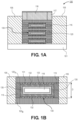
- the transistor device 100 comprises a substrate 101.
- the substrate 101 may be a semiconductor substrate or the like.
- a plurality of semiconductor channels 120 may be provided above the substrate 101.
- the semiconductor channels 120 may extend between source/drain regions 105.
- an interior spacer 115 may be provided at the ends of the of gate structure 130.
- the spacers 115 separate a gate structure 130 from the source/drain regions 105.
- Top spacers 117 are over the top most channel, and a gate fill metal 118 is between the top spacers 117.
- the gate structure 130 is provided between a pair of semiconductor channels 120. Typically, the space between the channels 120 is constrained. For example, the distance D between the semiconductor channel 120 A and the semiconductor channel 120 B may be approximately 10nm or smaller, or approximately 7nm or smaller.
- the gate structure 130 may include an interface layer 131 over and in direct contact with the semiconductor channels 120.
- the interface layer 131 may comprise silicon and oxygen (e.g., silicon dioxide).
- a gate dielectric layer 132 may be provided over the interface layer 131.
- the gate dielectric layer 132 may be a high-k dielectric material.
- a gate metal 133 may be formed in contact with the gate dielectric layer 132.
- the gate metal 133 may be a workfunction metal.
- the gate metal 133 is a conformal layer, and lines the interior surfaces of the gate dielectric layer 132.
- a fill metal 118 may fill the remainder of the cavity between the semiconductor channels 120.
- the gate dielectric layer 132 is deposited with a conformal deposition process (e.g., atomic layer deposition (ALD)). As such, the gate dielectric layer 132 is deposited along sidewalls of the spacers 115. As shown, vertical portions 135 of the gate dielectric layer 132 are in direct contact with the spacers 115. Particularly, it is noted that the vertical portions 135 of the gate dielectric layer 132 serve no electrical purpose in the transistor device 100. However, the vertical portions 135 result in an increase in the parasitic capacitance of the transistor device 100. As such, the switching speed is slowed down. This decreases the overall frequency of the processor.
- ALD atomic layer deposition
- embodiments disclosed herein include GAA transistor devices that omit the vertical portions 135 of the gate dielectric layer 132.
- the vertical portions 135 are omitted by using a selective deposition process.
- a liner is provided around the surfaces of the spacers.
- the liner is a material that prevents the deposition of the gate dielectric layer 132.
- the gate dielectric layer 132 will deposit on the interface layer 131 over the semiconductor channels 120 without depositing on the spacers 115. Without the presence of the vertical portions 135, parasitic capacitance is reduced, and device performance is improved.
- the removal of the vertical portions 135 also frees up room in the constrained volume between the semiconductor channels.
- the extra room is occupied by the spacers 115. That is, the width of the spacers 115 can be increased. Thicker spacers 115 results in a reduction in the parasitic capacitance.
- the extra room is occupied by the gate metal 133. Providing more volume for the gate metal 133 lowers the gate resistance. Accordingly, embodiments provide new architectures for GAA transistor devices that result in an increase in device performance.
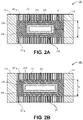
- the transistor 200 may comprise a plurality of semiconductor channels 220.
- a first semiconductor channel 220 A and a second semiconductor channel 220 B are shown.
- the semiconductor channels 220 may be any suitable semiconductor material.
- the semiconductor channels 220 comprise silicon.
- a distance D between the semiconductor channels 220 A and 220 B may be approximately 10nm or less, or approximately 7nm or less.
- approximately refers to a value that is within 10% of the stated value.
- approximately 10nm may refer to a range between 9nm and 11nm.
- ends of the semiconductor channels 220 may be connected to source/drain regions 205.
- the source/drain regions 205 may be epitaxially grown semiconductor material.
- the source/drain regions 205 may be heavily doped.
- a gate structure 230 is provided between the semiconductor channels 220.
- the gate structure 230 may comprise an interface layer 231.
- the interface layer 231 may be directly in contact with the semiconductor channels 220.
- the interface layer 231 comprises silicon and oxygen (e.g., SiOx).
- a gate dielectric 232 is provided over the interface layer 231.
- the gate dielectric 232 may be, for example, any suitable oxide such as silicon dioxide or high-k gate dielectric materials.
- high-k gate dielectric materials include, for instance, hafnium oxide, hafnium silicon oxide, lanthanum oxide, lanthanum aluminum oxide, zirconium oxide, zirconium silicon oxide, tantalum oxide, titanium oxide, barium strontium titanium oxide, barium titanium oxide, strontium titanium oxide, yttrium oxide, aluminum oxide, lead scandium tantalum oxide, and lead zinc niobate.
- an annealing process may be carried out on the gate dielectric 232 to improve its quality when a high-k material is used.
- the gate dielectric 232 In contrast to the GAA transistor 100, the gate dielectric 232 only covers the planar surfaces of the interface layer 231, and there is no vertical portion over sidewalls of the spacers 215. Particularly, a liner 240 that is provided over surface of the spacer 215 prevents the deposition of the gate dielectric 232 over the spacers 215.
- the liner 240 may be over a top surface of the spacer 215, an interior sidewall surface of the spacer 215 (i.e., the surface facing the gate structure 230), and a bottom surface of the spacer 215.
- the deposition process of the gate dielectric 232 may not nucleate growth on the liner 240.
- the liner 240 comprises a material without a hydroxyl terminated surface. The lack of the hydroxyl terminated surface prevents nucleation of the high-k dielectric chemistry provided in the ALD process.
- the liner 240 comprises silicon and nitrogen (e.g., a silicon nitride), or the liner 240 comprises silicon and carbon (e.g., a silicon carbide).
- a thickness of the liner 240 may be smaller than a thickness of the gate dielectric 232.
- a thickness of the liner 240 may be approximately 1nm or smaller. While shown as providing no gate dielectric growth on the interior sidewall of the spacer 215, it is to be appreciated that a non-significant amount of the gate dielectric 232 may deposit on the liner 240 over the interior sidewalls of the spacer 215.
- a gate metal 233 may line the gate dielectrics 232 and the liner 240.
- the gate metal 233 may be a workfunction metal.
- the gate metal 233 preferably has a workfunction that is between about 3.9 eV and about 4.2 eV.
- N-type materials that may be used to form the gate metal 233 include, but are not limited to, hafnium, zirconium, titanium, tantalum, aluminum, and metal carbides that include these elements, i.e., titanium carbide, zirconium carbide, tantalum carbide, hafnium carbide and aluminum carbide.
- the gate metal 233 When the gate metal 233 will serve as a P-type workfunction metal, the gate metal 233 preferable has a workfunction that is between about 4.9 eV and about 5.2 eV.
- P-type materials that may be used to form the gate metal 233 include, but are not limited to, ruthenium, palladium, platinum, cobalt, nickel, and conductive metal oxides, e.g., ruthenium oxide.
- a width W of the spacers 215 may be increased compared to the spacer dimensions shown in Figure 1B .
- a width W of the spacers 215 may be approximately 10nm or smaller, or approximately 5nm or smaller.
- the width W of the spacers 215 may be increased by an amount equal to the thickness of the gate dielectric 232. Increasing the thickness of the spacers 215 results in a lowering of the parasitic capacitance of the transistor 200. As such, switching frequency can be improved.
- FIG. 2B a cross-sectional illustration of a GAA transistor 200 is shown, in accordance with an additional embodiment.
- the transistor 200 in Figure 2B may be substantially similar to the transistor 200 in Figure 2A , with the exception of the width of the spacers 215.
- the extra room provided by omitting vertical portions of the gate dielectric 232 is occupied by the gate metal 233. That is, the gate metal 233 is increased in volume compared to the gate metal 233 shown in Figure 2A . Increasing the volume of the gate metal 233 results in a decrease in the gate resistance. As such, performance of the GAA transistor 200 is improved.
- the extra space is occupied by either the spacers 215 or the gate metal 233.
- the extra space may be occupied by increasing the volume of the gate metal 233 and increasing the width of the spacers 215. That is, a balance between increased gate metal 233 volume and increased spacer 215 width may selected in order to provide a desired performance to the transistor 200.
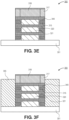
- FIG. 3A-3K a series of cross-sectional illustrations depicting a process for forming a GAA transistor device 300 is shown, in accordance with an embodiment.
- a transistor device 300 similar to the transistor device 200 shown in Figure 2B is shown.
- similar processing operations, with minor modifications, can be used to fabricate transistor devices 300 that are similar to any of the embodiments described herein.
- a stack of alternating semiconductor channels 320 and sacrificial layers 321 may be provided over a substrate 301.
- the underlying substrate 301 represents a general workpiece object used to manufacture integrated circuits.
- the substrate 301 often includes a wafer or other piece of silicon or another semiconductor material.
- Suitable semiconductor substrates include, but are not limited to, single crystal silicon, polycrystalline silicon and silicon on insulator (SOI), as well as similar substrates formed of other semiconductor materials, such as substrates including germanium, carbon, or group III-V materials.
- the semiconductor channels 320 and the sacrificial layers 321 may be materials that are etch selective to each other. That is, the sacrificial layers 321 may be etched without significantly etching the semiconductor channels 320.
- Semiconductor channels 320 and sacrificial layers 321 may each be a material such as, but not limited to, silicon, germanium, SiGe, GaAs, InSb, GaP, GaSb, InAlAs, InGaAs, GaSbP, GaAsSb, and InP.
- semiconductor channels 320 are silicon and sacrificial layers 321 are SiGe.
- semiconductor channels 320 are germanium, and sacrificial layers 321 are SiGe.
- a top spacer 317 may be provided over a top most semiconductor layer 320.
- a sacrificial gate structure 318 may also be provided over the top most semiconductor layer 320.
- the sacrificial gate structure 318 may be a polysilicon or another sacrificial material. That is, the sacrificial gate structure 318 may be removed in a subsequent processing operation in order to provide access to the semiconductor channels 320.
- the transistor 300 includes recessed sacrificial layers 321 to form cavities 351. Particularly, the ends of the sacrificial layers 321 are recessed so that a length of the sacrificial layers 321 is smaller than a length of the semiconductor channels 320.
- the sacrificial layer 321 may be etched with any suitable etching process.
- sacrificial layer 321 is recessed by a timed wet etch process. The selectivity of the etchant is greater than 50:1 for sacrificial layer 321 material over semiconductor channel 320 material.
- the selectivity is greater than 100:1.
- sacrificial layers 321 are selectively recessed using a wet etchant such as, but not limited to, aqueous carboxylic acid/nitric acid/HF solution and aqueous citric acid/nitric acid/HF solution.
- sacrificial layers 320 are selectively recessed using a wet etchant such as, but not limited to, ammonium hydroxide (NH4OH), tetramethylammonium hydroxide (TMAH), ethylenediamine pyrocatechol (EDP), or potassium hydroxide (KOH) solution.
- a wet etchant such as, but not limited to, ammonium hydroxide (NH4OH), tetramethylammonium hydroxide (TMAH), ethylenediamine pyrocatechol (EDP), or potassium hydroxide (KOH) solution.
- the liner 340 may be a conformally deposited material (e.g., a material deposited with ALD or the like).
- the liner 340 may comprise a material that inhibits the deposition of the material used to form the gate dielectric.
- the liner 340 may comprise silicon and nitrogen (e.g., a silicon nitride) or silicon and carbon (e.g., a silicon carbide).
- the liner 340 may have a thickness that is approximately 1nm or smaller.
- the liner 340 covers the sidewall surfaces of the sacrificial layers 321. Additionally, the liner 340 wraps around the exposed ends of the semiconductor channels 320. The liner 340 may also cover the spacer 317 and sacrificial gate structure 318.
- a spacer layer 315 is disposed over the substrate 301 and around the stack of semiconductor channels 320 and the sacrificial layers 321.
- the spacer layer 315 may be any suitable insulating material.
- the spacer layer 315 may be an oxide or a nitride.
- the spacer layer 315 may be deposited with a chemical vapor deposition (CVD) process, an ALD process, or the like.
- the spacer layer 315 is recessed so that only portions of the spacer 315 remain at the ends of the sacrificial layers 321.
- the spacer layer 315 may be recessed with an etching process.
- the etching process may also remove the liner 340 from over the ends of the semiconductor channels 320.
- the liner 340 remains over a top surface of the spacer 315, a bottom surface of the spacer 315, and an interior surface of the spacer 315 (i.e., the surface facing the sacrificial layer 321).
- the transistor 300 may include the growth of source/drain regions 305.
- the source/drain regions 305 may be epitaxially grown from the ends of the semiconductor channels 320 and/or from the underlying substrate 301.
- the source/drain regions 305 may be a silicon alloy such as, an in-situ doped silicon germanium, an in-situ doped silicon carbide, or an in-situ doped silicon. In alternate implementations, other silicon alloys may be used.
- alternate silicon alloy materials that may be used include, but are not limited to, nickel silicide, titanium silicide, cobalt silicide, and possibly may be doped with one or more of boron and/or aluminum.
- a CVD process may be used for the deposition of the source/drain regions 305.
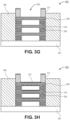
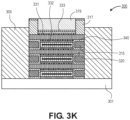
- FIG. 3G a cross-sectional illustration of the transistor 300 at a stage of manufacture is shown, in accordance with an embodiment.
- the sacrificial gate structure 318 is removed, and the sacrificial layers 321 are fully removed.
- any suitable etching chemistry such as those described above, may be used to remove the sacrificial layers 321. Removal of the sacrificial layers 321 results in a cavity 352 that exposes the semiconductor channels 320 and the liner 340 over the interior surface of the spacers 315.
- an interface layer 331 is formed over the exposed surfaces of the semiconductor channels 320.
- the interface layer 331 may comprise silicon and oxygen (e.g., SiOx).
- a gate dielectric 332 is deposited over the interface layers 331.
- the gate dielectric 332 may be selectively deposited over the interface layers 331 without depositing along the liner 340 on the interior surface of the spacers 315. As such, there is substantially no vertical portion of the gate dielectric 332. It is to be appreciated that the gate dielectric 332 may contact the liner 340 at the top and bottom of the spacer 315, but this contact arises from the growth of the gate dielectric 332 from the interface layer 331.
- the gate dielectric 332 may be deposited with a conformal deposition process, such as an ALD process.
- the material for the gate dielectric 332 may be similar to gate dielectric materials described in greater detail above.
- a gate metal 333 is deposited over the gate dielectric 332.
- the gate metal 333 may contact the gate dielectric 332 and the liner 340. Due to the absence of a vertical portion of the gate dielectric 332, the volume of the gate metal 333 may be increased.
- the gate metal 333 may be deposited with an ALD process, a CVD process, or the like.
- the gate metal 333 may be a workfunction metal, such as the workfunction metals described in greater detail above.
- a gate fill metal 319 may be disposed over the gate structure.
- the gate fill metal 319 may fill cavities between the semiconductor channels 320.
- the gate fill metal 319 may be provided between the top spacers 317.
- the gate fill metal 319 may include materials such as polysilicon, silicon nitride, silicon carbide, or various suitable metals or metal alloys, such as aluminum (Al), tungsten (W), titanium (Ti), tantalum (Ta), copper (Cu), titanium nitride (TiN), or tantalum nitride (TaN), for example.
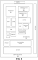
- FIG. 4 illustrates a computing device 400 in accordance with one implementation of an embodiment of the disclosure.
- the computing device 400 houses a board 402.
- the board 402 may include a number of components, including but not limited to a processor 404 and at least one communication chip 406.
- the processor 404 is physically and electrically coupled to the board 402.
- the at least one communication chip 406 is also physically and electrically coupled to the board 402.
- the communication chip 406 is part of the processor 404.
- computing device 400 may include other components that may or may not be physically and electrically coupled to the board 402. These other components include, but are not limited to, volatile memory (e.g., DRAM), non-volatile memory (e.g., ROM), flash memory, a graphics processor, a digital signal processor, a crypto processor, a chipset, an antenna, a display, a touchscreen display, a touchscreen controller, a battery, an audio codec, a video codec, a power amplifier, a global positioning system (GPS) device, a compass, an accelerometer, a gyroscope, a speaker, a camera, and a mass storage device (such as hard disk drive, compact disk (CD), digital versatile disk (DVD), and so forth).
- volatile memory e.g., DRAM
- non-volatile memory e.g., ROM
- flash memory e.g., a graphics processor, a digital signal processor, a crypto processor, a chipset, an antenna, a
- the communication chip 406 enables wireless communications for the transfer of data to and from the computing device 400.
- wireless and its derivatives may be used to describe circuits, devices, systems, methods, techniques, communications channels, etc., that may communicate data through the use of modulated electromagnetic radiation through a non-solid medium. The term does not imply that the associated devices do not contain any wires, although in some embodiments they might not.
- the communication chip 406 may implement any of a number of wireless standards or protocols, including but not limited to Wi-Fi (IEEE 802.11 family), WiMAX (IEEE 802.16 family), IEEE 802.20, long term evolution (LTE), Ev-DO, HSPA+, HSDPA+, HSUPA+, EDGE, GSM, GPRS, CDMA, TDMA, DECT, Bluetooth, derivatives thereof, as well as any other wireless protocols that are designated as 3G, 4G, 5G, and beyond.
- the computing device 400 may include a plurality of communication chips 406.
- a first communication chip 406 may be dedicated to shorter range wireless communications such as Wi-Fi and Bluetooth and a second communication chip 406 may be dedicated to longer range wireless communications such as GPS, EDGE, GPRS, CDMA, WiMAX, LTE, Ev-DO, and others.
- the processor 404 of the computing device 400 includes an integrated circuit die packaged within the processor 404.
- the integrated circuit die of the processor may comprise a GAA transistor device with a liner over the interior spacers that prohibits growth of the gate dielectric, as described herein.
- the term "processor" may refer to any device or portion of a device that processes electronic data from registers and/or memory to transform that electronic data into other electronic data that may be stored in registers and/or memory.
- the communication chip 406 also includes an integrated circuit die packaged within the communication chip 406.
- the integrated circuit die of the communication chip may comprise a GAA transistor device with a liner over the interior spacers that prohibits growth of the gate dielectric, as described herein.
- another component housed within the computing device 400 may comprise a GAA transistor device with a liner over the interior spacers that prohibits growth of the gate dielectric, as described herein.
- the computing device 400 may be a laptop, a netbook, a notebook, an ultrabook, a smartphone, a tablet, a personal digital assistant (PDA), an ultra mobile PC, a mobile phone, a desktop computer, a server, a printer, a scanner, a monitor, a set-top box, an entertainment control unit, a digital camera, a portable music player, or a digital video recorder.
- the computing device 400 may be any other electronic device that processes data.
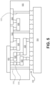
- FIG. 5 illustrates an interposer 500 that includes one or more embodiments of the disclosure.
- the interposer 500 is an intervening substrate used to bridge a first substrate 502 to a second substrate 504.
- the first substrate 502 may be, for instance, an integrated circuit die.
- the second substrate 504 may be, for instance, a memory module, a computer motherboard, or another integrated circuit die.
- one of both of the first substrate 502 and the second substrate 504 may comprise a GAA transistor device with a liner over the interior spacers that prohibits growth of the gate dielectric, in accordance with embodiments described herein.
- the purpose of an interposer 500 is to spread a connection to a wider pitch or to reroute a connection to a different connection.
- an interposer 500 may couple an integrated circuit die to a ball grid array (BGA) 506 that can subsequently be coupled to the second substrate 504.
- BGA ball grid array
- the first and second substrates 502/504 are attached to opposing sides of the interposer 500.
- the first and second substrates 502/504 are attached to the same side of the interposer 500.
- three or more substrates are interconnected by way of the interposer 500.
- the interposer 500 may be formed of an epoxy resin, a fiberglass-reinforced epoxy resin, a ceramic material, or a polymer material such as polyimide. In further implementations, the interposer 500 may be formed of alternate rigid or flexible materials that may include the same materials described above for use in a semiconductor substrate, such as silicon, germanium, and other group III-V and group IV materials.
- the interposer 500 may include metal interconnects 508 and vias 510, including but not limited to through-silicon vias (TSVs) 512.
- the interposer 500 may further include embedded devices 514, including both passive and active devices.
- Such devices include, but are not limited to, capacitors, decoupling capacitors, resistors, inductors, fuses, diodes, transformers, sensors, and electrostatic discharge (ESD) devices.
- More complex devices such as radiofrequency (RF) devices, power amplifiers, power management devices, antennas, arrays, sensors, and MEMS devices may also be formed on the interposer 500.
- apparatuses or processes disclosed herein may be used in the fabrication of interposer 500.
- embodiments of the present disclosure may comprise a GAA transistor device with a liner over the interior spacers that prohibits growth of the gate dielectric.
- Example 1 a transistor device, comprising: a first channel, wherein the first channel comprises a semiconductor material; a second channel above the first channel, wherein the second channel comprises the semiconductor material; a first spacer between the first channel and the second channel; a second spacer between the first channel and the second channel; a first gate dielectric over a surface of the first channel that faces the second channel; and a second gate dielectric over a surface of the second channel that faces the first channel, wherein the first gate dielectric is physically separated from the second gate dielectric.
- Example 2 the transistor device of Example 1, further comprising a first interface layer between the first gate dielectric and the surface of the first channel and a second interface layer between the second gate dielectric and the second channel.
- Example 3 the transistor device of Example 2, wherein the first interface layer and the second interface layer comprise silicon and oxygen.
- Example 4 the transistor device of Examples 1-3, further comprising: a liner around the first spacer and the second spacer.
- Example 5 the transistor device of Example 4, wherein the liner covers three surfaces of the first spacer and three surfaces of the second spacer.
- Example 6 the transistor device of Example 4 or Example 5, wherein the liner comprises silicon and nitrogen.
- Example 7 the transistor device of Example 4 or Example 5, wherein the liner comprises silicon and carbon.
- Example 8 the transistor device of Examples 4-7, wherein a thickness of the liner is smaller than a thickness of the first gate dielectric.
- Example 9 the transistor device of Example 8, wherein the thickness of the liner is 1nm or smaller.
- Example 10 the transistor device of Examples 1-9, further comprising: a metal layer between the first channel and the second channel.
- Example 11 the transistor device of Example 10, wherein the metal layer is over the first channel, the second channel, the first spacer, and the second spacer.
- Example 12 the transistor device of Examples 1-11, wherein a distance between the first channel and the second channel is approximately 10nm or smaller.
- Example 13 a method of forming a transistor device, comprising: forming a stack, wherein the stack comprises a plurality of channels that alternate with a plurality of sacrificial layers; recessing ends of the sacrificial layers; disposing a liner on the sacrificial layers and around ends of the plurality of channels; disposing spacers adjacent to the ends of the sacrificial layers; forming a source region and a drain region on opposite ends of the plurality of channels, wherein the source region and the drain region directly contact the plurality of channels; removing the sacrificial layers; disposing a gate dielectric over the plurality of channels, wherein the gate dielectric does not substantially deposit on the liner over the spacers; and disposing a gate metal over the gate dielectric.
- Example 14 the method of Example 13, wherein the liner has a thickness that is less than a thickness of the gate dielectric.
- Example 15 the method of Example 14, wherein the thickness of the liner is 1nm or smaller.
- Example 16 the method of Examples 13-15, wherein the liner comprises a material without a hydroxyl terminated surface.
- Example 17 the method of Example 16, wherein the liner comprises silicon and carbon or silicon and nitrogen.
- Example 18 the method of Examples 13-17, wherein the gate metal is separated from the spacer by the liner.
- Example 19 the method of Examples 13-18, wherein the liner wraps around the spacers.
- Example 20 the method of Example 19, wherein the liner is over a top surface of the spacers, an interior surface of the spacers, and a bottom surface of the spacers.
- Example 21 the method of Examples 13-19, wherein a distance between the plurality of channels is approximately 10nm or smaller.
- Example 22 an electronic system, comprising: a board; a package substrate coupled to the board; and a die coupled to the package substrate, wherein the die comprise a transistor device, comprising: a first channel, wherein the first channel comprises a semiconductor material; a second channel above the first channel, wherein the second channel comprises the semiconductor material; a first spacer between the first channel and the second channel; a second spacer between the first channel and the second channel; a first gate dielectric over a surface of the first channel that faces the second channel; and a second gate dielectric over a surface of the second channel that faces the first channel, wherein the first gate dielectric is physically separated from the second gate dielectric.
- a transistor device comprising: a first channel, wherein the first channel comprises a semiconductor material; a second channel above the first channel, wherein the second channel comprises the semiconductor material; a first spacer between the first channel and the second channel; a second spacer between the first channel and the second channel; a first gate dielectric over a surface of the first channel that faces
- Example 23 the electronic system of Example 22, further comprising: a liner around the first spacer and the second spacer.
- Example 24 the electronic system of Example 23, wherein the liner covers three surfaces of the first spacer and three surfaces of the second spacer, and wherein trace amounts of a gate dielectric material are provided over vertical surfaces of the liner.
- Example 25 the electronic system of Example 23 or Example 24, wherein the liner comprises silicon and nitrogen, or silicon and carbon.
Landscapes
- Insulated Gate Type Field-Effect Transistor (AREA)
- Electrodes Of Semiconductors (AREA)
- Engineering & Computer Science (AREA)
- Manufacturing & Machinery (AREA)
Applications Claiming Priority (1)
| Application Number | Priority Date | Filing Date | Title |
|---|---|---|---|
| US17/485,238 US12610584B2 (en) | 2021-09-24 | 2021-09-24 | Selective growth of high-k oxide on channel of gate-all-around transistors |
Publications (1)
| Publication Number | Publication Date |
|---|---|
| EP4156291A1 true EP4156291A1 (de) | 2023-03-29 |
Family
ID=82846318
Family Applications (1)
| Application Number | Title | Priority Date | Filing Date |
|---|---|---|---|
| EP22184357.6A Pending EP4156291A1 (de) | 2021-09-24 | 2022-07-12 | Selektives wachstum von high-k-oxid auf einem kanal von gate-all-around-transistoren |
Country Status (3)
| Country | Link |
|---|---|
| US (1) | US12610584B2 (de) |
| EP (1) | EP4156291A1 (de) |
| CN (1) | CN115863430A (de) |
Families Citing this family (3)
| Publication number | Priority date | Publication date | Assignee | Title |
|---|---|---|---|---|
| US12288783B2 (en) * | 2021-11-04 | 2025-04-29 | Taiwan Semiconductor Manufacturing Company, Ltd. | Integrated standard cell structure |
| US20240072114A1 (en) * | 2022-08-30 | 2024-02-29 | Taiwan Semiconductor Manufacturing Company, Ltd. | Semiconductor device having nanosheet transistor and methods of fabrication thereof |
| CN119815824B (zh) * | 2023-10-08 | 2025-12-12 | 北京超弦存储器研究院 | 半导体结构的制备方法及半导体结构 |
Citations (5)
| Publication number | Priority date | Publication date | Assignee | Title |
|---|---|---|---|---|
| US20190067441A1 (en) * | 2017-08-30 | 2019-02-28 | Taiwan Semiconductor Manufacturing Co., Ltd. | Method of manufacturing a semiconductor device and a semiconductor device |
| US20190148151A1 (en) * | 2017-11-15 | 2019-05-16 | Taiwan Semiconductor Manufacturing Company, Ltd. | Selective High-K Formation in Gate-Last Process |
| US20210104522A1 (en) * | 2019-10-03 | 2021-04-08 | Tokyo Electron Limited | High performance nanosheet fabrication method with enhanced high mobility channel elements |
| US20210184000A1 (en) * | 2019-12-13 | 2021-06-17 | Intel Corporation | Single gated 3d nanowire inverter for high density thick gate soc applications |
| EP3979329A2 (de) * | 2020-10-05 | 2022-04-06 | Samsung Electronics Co., Ltd. | Halbleiterbauelement und verfahren zur herstellung davon |
Family Cites Families (2)
| Publication number | Priority date | Publication date | Assignee | Title |
|---|---|---|---|---|
| US10269965B1 (en) * | 2017-10-25 | 2019-04-23 | Taiwan Semiconductor Manufacturing Company Ltd. | Multi-gate semiconductor device and method for forming the same |
| US11538937B2 (en) * | 2019-01-04 | 2022-12-27 | Intel Corporation | Fin trim plug structures having an oxidation catalyst layer surrounded by a recessed dielectric material |
-
2021
- 2021-09-24 US US17/485,238 patent/US12610584B2/en active Active
-
2022
- 2022-07-12 EP EP22184357.6A patent/EP4156291A1/de active Pending
- 2022-08-24 CN CN202211019872.3A patent/CN115863430A/zh active Pending
Patent Citations (5)
| Publication number | Priority date | Publication date | Assignee | Title |
|---|---|---|---|---|
| US20190067441A1 (en) * | 2017-08-30 | 2019-02-28 | Taiwan Semiconductor Manufacturing Co., Ltd. | Method of manufacturing a semiconductor device and a semiconductor device |
| US20190148151A1 (en) * | 2017-11-15 | 2019-05-16 | Taiwan Semiconductor Manufacturing Company, Ltd. | Selective High-K Formation in Gate-Last Process |
| US20210104522A1 (en) * | 2019-10-03 | 2021-04-08 | Tokyo Electron Limited | High performance nanosheet fabrication method with enhanced high mobility channel elements |
| US20210184000A1 (en) * | 2019-12-13 | 2021-06-17 | Intel Corporation | Single gated 3d nanowire inverter for high density thick gate soc applications |
| EP3979329A2 (de) * | 2020-10-05 | 2022-04-06 | Samsung Electronics Co., Ltd. | Halbleiterbauelement und verfahren zur herstellung davon |
Also Published As
| Publication number | Publication date |
|---|---|
| US12610584B2 (en) | 2026-04-21 |
| CN115863430A (zh) | 2023-03-28 |
| US20230100505A1 (en) | 2023-03-30 |
Similar Documents
| Publication | Publication Date | Title |
|---|---|---|
| US12382706B2 (en) | Self-aligned gate endcap (SAGE) architectures with gate-all-around devices | |
| US10453967B2 (en) | Semiconductor nanowire device having cavity spacer and method of fabricating cavity spacer for semiconductor nanowire device | |
| US12457771B2 (en) | Plug and recess process for dual metal gate on stacked nanoribbon devices | |
| EP4156291A1 (de) | Selektives wachstum von high-k-oxid auf einem kanal von gate-all-around-transistoren | |
| US11990476B2 (en) | Semiconductor nanowire device having (111)-plane channel sidewalls | |
| US12342612B2 (en) | Neighboring gate-all-around integrated circuit structures having disjoined epitaxial source or drain regions | |
| US12288813B2 (en) | Gate-all-around integrated circuit structures having insulator fin on insulator substrate | |
| US12396254B2 (en) | Stacked 2D CMOS with inter metal layers | |
| US20260114007A1 (en) | Self-aligned gate endcap (sage) architectures with gate-all-around devices above insulator substrates | |
| EP4109547A1 (de) | Nanoband-subfinnen-isolierung durch rückseitiges entfernen des siliziumsubstrats mit epi-schutz | |
| CN114664823A (zh) | 在外延源极或漏极区之间具有导电接触应力源的相邻全环栅集成电路结构 | |
| US20230317809A1 (en) | Selective passivation for epi growth in presence of metallic contacts | |
| EP4109553A1 (de) | Siliziumreiche schicht mit niedrigem germaniumgehalt für pmos-kontaktwiderstands-thermostabilität | |
| US20240105770A1 (en) | Necked ribbon for better n workfunction filling and device performance | |
| EP4300588A1 (de) | Kontaktarchitektur für 2d-stapelnanobandtransistor | |
| EP4156288A1 (de) | Hoch-k- oder ferroelektrisches gate-oxid mit null-sio2 il prozess für transistor | |
| US12317585B2 (en) | Adjacent gate-all-around integrated circuit structures having non-merged epitaxial source or drain regions | |
| TW202329328A (zh) | 具有針對磊晶源極或汲極區域界限之凸起壁結構的環繞式閘極積體電路結構 | |
| US12622250B2 (en) | Vias with vertically non-uniform or discontinuous stack | |
| US20230317563A1 (en) | Vias with vertically non-uniform or discontinuous stack | |
| EP4156296A1 (de) | Beseitigung von unterlamellenlecks in gestapelten nanofolienarchitekturen | |
| US20230096347A1 (en) | Cmos integration of 2d material by end etch | |
| US20230207466A1 (en) | Recessed and self-aligned buried power rail |
Legal Events
| Date | Code | Title | Description |
|---|---|---|---|
| PUAI | Public reference made under article 153(3) epc to a published international application that has entered the european phase |
Free format text: ORIGINAL CODE: 0009012 |
|
| STAA | Information on the status of an ep patent application or granted ep patent |
Free format text: STATUS: THE APPLICATION HAS BEEN PUBLISHED |
|
| AK | Designated contracting states |
Kind code of ref document: A1 Designated state(s): AL AT BE BG CH CY CZ DE DK EE ES FI FR GB GR HR HU IE IS IT LI LT LU LV MC MK MT NL NO PL PT RO RS SE SI SK SM TR |
|
| STAA | Information on the status of an ep patent application or granted ep patent |
Free format text: STATUS: REQUEST FOR EXAMINATION WAS MADE |
|
| 17P | Request for examination filed |
Effective date: 20230928 |
|
| RBV | Designated contracting states (corrected) |
Designated state(s): AL AT BE BG CH CY CZ DE DK EE ES FI FR GB GR HR HU IE IS IT LI LT LU LV MC MK MT NL NO PL PT RO RS SE SI SK SM TR |