EP4156232A1 - Speicheranordnungen mit ferroelektrischen materialien auf nitridbasis - Google Patents
Speicheranordnungen mit ferroelektrischen materialien auf nitridbasis Download PDFInfo
- Publication number
- EP4156232A1 EP4156232A1 EP22190629.0A EP22190629A EP4156232A1 EP 4156232 A1 EP4156232 A1 EP 4156232A1 EP 22190629 A EP22190629 A EP 22190629A EP 4156232 A1 EP4156232 A1 EP 4156232A1
- Authority
- EP
- European Patent Office
- Prior art keywords
- nitride
- plateline
- memory device
- node
- based ferroelectric
- Prior art date
- Legal status (The legal status is an assumption and is not a legal conclusion. Google has not performed a legal analysis and makes no representation as to the accuracy of the status listed.)
- Granted
Links
Images

Classifications
-
- H—ELECTRICITY
- H10—SEMICONDUCTOR DEVICES; ELECTRIC SOLID-STATE DEVICES NOT OTHERWISE PROVIDED FOR
- H10B—ELECTRONIC MEMORY DEVICES
- H10B53/00—Ferroelectric RAM [FeRAM] devices comprising ferroelectric memory capacitors
- H10B53/30—Ferroelectric RAM [FeRAM] devices comprising ferroelectric memory capacitors characterised by the memory core region
-
- H—ELECTRICITY
- H10—SEMICONDUCTOR DEVICES; ELECTRIC SOLID-STATE DEVICES NOT OTHERWISE PROVIDED FOR
- H10D—INORGANIC ELECTRIC SEMICONDUCTOR DEVICES
- H10D1/00—Resistors, capacitors or inductors
- H10D1/60—Capacitors
- H10D1/68—Capacitors having no potential barriers
-
- H—ELECTRICITY
- H10—SEMICONDUCTOR DEVICES; ELECTRIC SOLID-STATE DEVICES NOT OTHERWISE PROVIDED FOR
- H10B—ELECTRONIC MEMORY DEVICES
- H10B53/00—Ferroelectric RAM [FeRAM] devices comprising ferroelectric memory capacitors
- H10B53/20—Ferroelectric RAM [FeRAM] devices comprising ferroelectric memory capacitors characterised by the three-dimensional arrangements, e.g. with cells on different height levels
-
- H—ELECTRICITY
- H10—SEMICONDUCTOR DEVICES; ELECTRIC SOLID-STATE DEVICES NOT OTHERWISE PROVIDED FOR
- H10D—INORGANIC ELECTRIC SEMICONDUCTOR DEVICES
- H10D1/00—Resistors, capacitors or inductors
- H10D1/60—Capacitors
- H10D1/68—Capacitors having no potential barriers
- H10D1/692—Electrodes
- H10D1/711—Electrodes having non-planar surfaces, e.g. formed by texturisation
- H10D1/716—Electrodes having non-planar surfaces, e.g. formed by texturisation having vertical extensions
Definitions
- Embodiments of the disclosure are in the field of advanced integrated circuit structure fabrication and, in particular, memory devices with nitride-based ferroelectric materials.
- Tri-gate transistors In the manufacture of integrated circuit devices, multi-gate transistors, such as tri-gate transistors, have become more prevalent as device dimensions continue to scale down. Tri-gate transistors are generally fabricated on either bulk silicon substrates or silicon-on-insulator substrates. In some instances, bulk silicon substrates are preferred due to their lower cost and compatibility with the existing high-yielding bulk silicon substrate infrastructure.
- Coupled means that one element or node or feature is directly or indirectly joined to (or directly or indirectly communicates with) another element or node or feature, and not necessarily mechanically.
- inhibit is used to describe a reducing or minimizing effect. When a component or feature is described as inhibiting an action, motion, or condition it may completely prevent the result or outcome or future state completely. Additionally, “inhibit” can also refer to a reduction or lessening of the outcome, performance, or effect which might otherwise occur. Accordingly, when a component, element, or feature is referred to as inhibiting a result or state, it need not completely prevent or eliminate the result or state.
- Embodiments described herein may be directed to front-end-of-line (FEOL) semiconductor processing and structures.
- FEOL is the first portion of integrated circuit (IC) fabrication where the individual devices (e.g., transistors, capacitors, resistors, etc.) are patterned in the semiconductor substrate or layer.
- FEOL generally covers everything up to (but not including) the deposition of metal interconnect layers. Following the last FEOL operation, the result is typically a wafer with isolated transistors (e.g., without any wires).
- Embodiments described herein may be directed to back-end-of-line (BEOL) semiconductor processing and structures.
- BEOL is the second portion of IC fabrication where the individual devices (e.g., transistors, capacitors, resistors, etc.) get interconnected with wiring on the wafer, e.g., the metallization layer or layers.
- BEOL includes contacts, insulating layers (dielectrics), metal levels, and bonding sites for chip-to-package connections.
- contacts pads
- interconnect wires, vias and dielectric structures are formed. For modern IC processes, more than 10 metal layers may be added in the BEOL.
- Embodiments described below may be applicable to FEOL processing and structures, BEOL processing and structures, or both FEOL and BEOL processing and structures.
- an exemplary processing scheme may be illustrated using a FEOL processing scenario, such approaches may also be applicable to BEOL processing.
- an exemplary processing scheme may be illustrated using a BEOL processing scenario, such approaches may also be applicable to FEOL processing.
- FRAM 3D ferroelectric RAM
- FeRAM FeRAM
- F-RAM 3D ferroelectric RAM
- a FRAM is a random-access memory similar in construction to DRAM but uses a ferroelectric layer instead of a dielectric layer to achieve non-volatility.
- both FRAM and DRAM are one transistor (1T)/one capacitor (1C) cell arrays, where each cell comprises an access transistor in the front end coupled to a single capacitor.
- the capacitor may be coupled to a bitline (COB) higher in the stack in the semiconductor back end.
- COB bitline
- embodiments of the present disclosure address these and other issues by providing novel memory device structures that use nitride-based ferroelectrics.
- the memory devices of the present disclosure have significantly improved wakeup (e.g., near-zero wakeup) and stable remnant polarization during cycling and a sharp polarization curve relative to prior solutions. This helps to provide a memory array with an insignificant difference in switching field between devices, thereby reducing or eliminating read disturbances for devices sharing common bitlines.
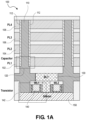
- FIG. 1A illustrates a cross-section view of an example of an IC structure comprising a memory device 100 in accordance with various embodiments.
- memory device 100 includes a node 110 and a plurality of platelines 102, 104, 106, and 108.
- a capacitor 120 is coupled to plateline 102, the capacitor 120 comprising a nitride-based ferroelectric material 112 between the plateline 102 and the node 110.
- the nitride-based ferroelectric material 112 includes aluminum scandium nitride (AIScN).
- AIScN of the nitride-based ferroelectric material 112 includes between 25% scandium (Sc) to 40% Sc.
- the nitride-based ferroelectric material 112 is layered in a superlattice.
- the nitride-based ferroelectric material 112 may be of any suitable dimension.
- the nitride-based ferroelectric material 112 has a thickness of between 3nm and 10nm.
- nitride-based ferroelectric material 112 has a length running substantially perpendicular to the platelines 102, 104, 106, 108 and "thickness" measured between, for example, plateline 102 and node 110.
- the thickness may be between 3nm and 10nm for AIScN and larger (wider) for different nitride-based ferroelectrics.
- Memory device 100 further includes a bitline 130 coupled to the node 110 and a wordline 140 coupled to the node110. Access transistor 142 is coupled to the bitline 130, the wordline 140, and the node 110.
- the wordline 140 is perpendicular to the platelines 102, 104, 106, 108, and the bitline 130 is parallel to the platelines.
- memory device 100 further includes a substrate layer 150. As shown in Figure 1A , substrate layer 150 comprises silicon, though the substrate layer 150 may include any suitable material or combination of materials.
- a memory device may include a wordline that is parallel to the plateline and a bitline that is perpendicular to the plateline.
- parallel and perpendicular are intended to mean “substantially parallel” and “substantially perpendicular.”
- two structures may be substantially parallel or substantially perpendicular within +/- 5 degrees.
- Figure 1B illustrates a memory device 160 with a plurality of platelines 102, 104, 106, and 108.
- a capacitor 120 is coupled to plateline 102, the capacitor 120 comprising a nitride-based ferroelectric material 112 between the plateline 102 and the node 110.
- memory device 160 includes a wordline 162 that is parallel to the platelines 102, 104, 106, 108, and a bitline 164 that is perpendicular to platelines 102, 104, 106, 108, with access transistor 166 coupled to the wordline 162, bitline 164, and node 110 as shown.
- the node 110 may comprise any suitable material or combination of materials.
- the node 110 comprises a multilayered electrode with a crystal orientation of Al(100).
- the node 110 may comprise a crystal orientation of Ti(111) or Pt(111).
- Embodiments of the present disclosure may include any suitable number of capacitors coupled to platelines 102, 104, 106, 108.
- plateline 102 may be coupled to a first capacitor comprising a nitride-based ferroelectric material between the first plateline 102 and the node 110, with a second capacitor 120 comprising the nitride-based ferroelectric material 112 between the second plateline 104 and the node 110.
- Implementations of embodiments of the invention may be formed or carried out on a substrate, such as a semiconductor substrate.
- the semiconductor substrate may be a crystalline substrate formed using a bulk silicon or a silicon-on-insulator substructure.
- the semiconductor substrate may be formed using alternate materials, which may or may not be combined with silicon, that include but are not limited to germanium, indium antimonide, lead telluride, indium arsenide, indium phosphide, gallium arsenide, indium gallium arsenide, gallium antimonide, or other combinations of group III-V or group IV materials. Although a few examples of materials from which the substrate may be formed are described here, any material that may serve as a foundation upon which a semiconductor device may be built falls within the scope of the present invention.
- MOSFET metal-oxide-semiconductor field-effect transistors
- the MOS transistors may be planar transistors, nonplanar transistors, or a combination of both.
- Nonplanar transistors include FinFET transistors such as double-gate transistors and tri-gate transistors, and wrap-around or all-around gate transistors such as nanoribbon and nanowire transistors.
- Each MOS transistor includes a gate stack formed of at least two layers, a gate dielectric layer and a gate electrode layer.
- the gate dielectric layer may include one layer or a stack of layers.
- the one or more layers may include silicon oxide, silicon dioxide (SiO 2 ) and/or a high-k dielectric material.
- the high-k dielectric material may include elements such as hafnium, silicon, oxygen, titanium, tantalum, lanthanum, aluminum, zirconium, barium, strontium, yttrium, lead, scandium, niobium, and zinc.
- high-k materials that may be used in the gate dielectric layer include, but are not limited to, hafnium oxide, hafnium silicon oxide, lanthanum oxide, lanthanum aluminum oxide, zirconium oxide, zirconium silicon oxide, tantalum oxide, titanium oxide, barium strontium titanium oxide, barium titanium oxide, strontium titanium oxide, yttrium oxide, aluminum oxide, lead scandium tantalum oxide, and lead zinc niobate.
- an annealing process may be carried out on the gate dielectric layer to improve its quality when a high-k material is used.
- the gate electrode layer is formed on the gate dielectric layer and may consist of at least one P-type workfunction metal or N-type workfunction metal, depending on whether the transistor is to be a PMOS or an NMOS transistor.
- the gate electrode layer may consist of a stack of two or more metal layers, where one or more metal layers are workfunction metal layers and at least one metal layer is a fill metal layer.
- metals that may be used for the gate electrode include, but are not limited to, ruthenium, palladium, platinum, cobalt, nickel, and conductive metal oxides, e.g., ruthenium oxide.
- a P-type metal layer will enable the formation of a PMOS gate electrode with a workfunction that is between about 4.9 eV and about 5.2 eV.
- metals that may be used for the gate electrode include, but are not limited to, hafnium, zirconium, titanium, tantalum, aluminum, alloys of these metals, and carbides of these metals such as hafnium carbide, zirconium carbide, titanium carbide, tantalum carbide, and aluminum carbide.
- An N-type metal layer will enable the formation of an NMOS gate electrode with a workfunction that is between about 3.9 eV and about 4.2 eV.
- the gate electrode may consist of a "U"-shaped structure that includes a bottom portion substantially parallel to the surface of the substrate and two sidewall portions that are substantially perpendicular to the top surface of the substrate.
- at least one of the metal layers that form the gate electrode may simply be a planar layer that is substantially parallel to the top surface of the substrate and does not include sidewall portions substantially perpendicular to the top surface of the substrate.
- the gate electrode may consist of a combination of U-shaped structures and planar, non-U-shaped structures.
- the gate electrode may consist of one or more U-shaped metal layers formed atop one or more planar, non-U-shaped layers.
- a pair of sidewall spacers may be formed on opposing sides of the gate stack that bracket the gate stack.
- the sidewall spacers may be formed from a material such as silicon nitride, silicon oxide, silicon carbide, silicon nitride doped with carbon, and silicon oxynitride. Processes for forming sidewall spacers are well known in the art and generally include deposition and etching process steps. In an alternate implementation, a plurality of spacer pairs may be used, for instance, two pairs, three pairs, or four pairs of sidewall spacers may be formed on opposing sides of the gate stack.
- source and drain regions are formed within the substrate adjacent to the gate stack of each MOS transistor.
- the source and drain regions are generally formed using either an implantation/diffusion process or an etching/deposition process.
- dopants such as boron, aluminum, antimony, phosphorous, or arsenic may be ion-implanted into the substrate to form the source and drain regions.
- An annealing process that activates the dopants and causes them to diffuse further into the substrate typically follows the ion implantation process.
- the substrate may first be etched to form recesses at the locations of the source and drain regions.
- the source and drain regions may be fabricated using a silicon alloy such as silicon germanium or silicon carbide.
- the epitaxially deposited silicon alloy may be doped in situ with dopants such as boron, arsenic, or phosphorous.
- the source and drain regions may be formed using one or more alternate semiconductor materials such as germanium or a group III-V material or alloy. And in further embodiments, one or more layers of metal and/or metal alloys may be used to form the source and drain regions.
- ILD interlayer dielectrics
- the ILD layers may be formed using dielectric materials known for their applicability in integrated circuit structures, such as low-k dielectric materials. Examples of dielectric materials that may be used include, but are not limited to, silicon dioxide (SiO 2 ), carbon doped oxide (CDO), silicon nitride, organic polymers such as perfluorocyclobutane or polytetrafluoroethylene, fluorosilicate glass (FSG), and organosilicates such as silsesquioxane, siloxane, or organosilicate glass.
- the ILD layers may include pores or air gaps to further reduce their dielectric constant.
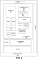
- FIG. 2 illustrates a computing device 200 in accordance with one implementation of the invention.
- the computing device 200 houses a board 202.
- the board 202 may include a number of components, including but not limited to a processor 204 and at least one communication chip 206.
- the processor 204 is physically and electrically coupled to the board 202.
- the at least one communication chip 206 is also physically and electrically coupled to the board 202.
- the communication chip 206 is part of the processor 204.
- computing device 200 may include other components that may or may not be physically and electrically coupled to the board 202.
- these other components include, but are not limited to, volatile memory (e.g., DRAM), non-volatile memory (e.g., ROM), flash memory, a graphics processor, a digital signal processor, a crypto processor, a chipset, an antenna, a display, a touchscreen display, a touchscreen controller, a battery, an audio codec, a video codec, a power amplifier, a global positioning system (GPS) device, a compass, an accelerometer, a gyroscope, a speaker, a camera, and a mass storage device (such as hard disk drive, compact disk (CD), digital versatile disk (DVD), and so forth).
- volatile memory e.g., DRAM
- non-volatile memory e.g., ROM
- flash memory e.g., a graphics processor, a digital signal processor, a crypto processor, a chipset, an antenna
- the communication chip 206 enables wireless communications for the transfer of data to and from the computing device 200.
- wireless and its derivatives may be used to describe circuits, devices, systems, methods, techniques, communications channels, etc., that may communicate data through the use of modulated electromagnetic radiation through a non-solid medium. The term does not imply that the associated devices do not contain any wires, although in some embodiments they might not.
- the communication chip 206 may implement any of a number of wireless standards or protocols, including but not limited to Wi-Fi (IEEE 802.11 family), WiMAX (IEEE 802.16 family), IEEE 802.20, long term evolution (LTE), Ev-DO, HSPA+, HSDPA+, HSUPA+, EDGE, GSM, GPRS, CDMA, TDMA, DECT, Bluetooth, derivatives thereof, as well as any other wireless protocols that are designated as 3G, 4G, 5G, and beyond.
- the computing device 200 may include a plurality of communication chips 206.
- a first communication chip 206 may be dedicated to shorter range wireless communications such as Wi-Fi and Bluetooth and a second communication chip 206 may be dedicated to longer range wireless communications such as GPS, EDGE, GPRS, CDMA, WiMAX, LTE, Ev-DO, and others.
- the processor 204 of the computing device 200 includes an integrated circuit die packaged within the processor 204.
- the integrated circuit die of the processor includes one or more devices, such as MOS-FET transistors built in accordance with implementations of the invention.
- the term "processor" may refer to any device or portion of a device that processes electronic data from registers and/or memory to transform that electronic data into other electronic data that may be stored in registers and/or memory.
- the communication chip 206 also includes an integrated circuit die packaged within the communication chip 206.
- the integrated circuit die of the communication chip includes one or more devices, such as MOS-FET transistors built in accordance with implementations of the invention.
- another component housed within the computing device 200 may contain an integrated circuit die that includes one or more devices, such as MOS-FET transistors built in accordance with implementations of the invention.
- the computing device 200 may be a laptop, a netbook, a notebook, an ultrabook, a smartphone, a tablet, a personal digital assistant (PDA), an ultra-mobile PC, a mobile phone, a desktop computer, a server, a printer, a scanner, a monitor, a set-top box, an entertainment control unit, a digital camera, a portable music player, or a digital video recorder.
- the computing device 200 may be any other electronic device that processes data.
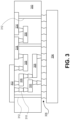
- FIG. 3 illustrates an interposer 300 that includes one or more embodiments of the invention.
- the interposer 300 is an intervening substrate used to bridge a first substrate 302 to a second substrate 304.
- the first substrate 302 may be, for instance, an integrated circuit die.
- the second substrate 304 may be, for instance, a memory module, a computer motherboard, or another integrated circuit die.
- the purpose of an interposer 300 is to spread a connection to a wider pitch or to reroute a connection to a different connection.
- an interposer 300 may couple an integrated circuit die to a ball grid array (BGA) 306 that can subsequently be coupled to the second substrate 304.
- BGA ball grid array
- the first and second substrates 302/304 are attached to opposing sides of the interposer 300.
- the first and second substrates 302/304 are attached to the same side of the interposer 300.
- three or more substrates are interconnected by way of the interposer 300.
- the interposer 300 may be formed of an epoxy resin, a fiberglass-reinforced epoxy resin, a ceramic material, or a polymer material such as polyimide. In further implementations, the interposer 300 may be formed of alternate rigid or flexible materials that may include the same materials described above for use in a semiconductor substrate, such as silicon, germanium, and other group III-V and group IV materials.
- the interposer 300 may include metal interconnects 308 and vias 310, including but not limited to through-silicon vias (TSVs) 312.
- the interposer 300 may further include embedded devices 314, including both passive and active devices.
- Such devices include, but are not limited to, capacitors, decoupling capacitors, resistors, inductors, fuses, diodes, transformers, sensors, and electrostatic discharge (ESD) devices.
- More complex devices such as radio-frequency (RF) devices, power amplifiers, power management devices, antennas, arrays, sensors, and MEMS devices may also be formed on the interposer 300.
- apparatuses or processes disclosed herein may be used in the fabrication of interposer 300.
Landscapes
- Semiconductor Memories (AREA)
Applications Claiming Priority (1)
| Application Number | Priority Date | Filing Date | Title |
|---|---|---|---|
| US17/485,305 US20230116719A1 (en) | 2021-09-24 | 2021-09-24 | Memory devices with nitride-based ferroelectric materials |
Publications (2)
| Publication Number | Publication Date |
|---|---|
| EP4156232A1 true EP4156232A1 (de) | 2023-03-29 |
| EP4156232B1 EP4156232B1 (de) | 2025-09-10 |
Family
ID=83271006
Family Applications (1)
| Application Number | Title | Priority Date | Filing Date |
|---|---|---|---|
| EP22190629.0A Active EP4156232B1 (de) | 2021-09-24 | 2022-08-16 | Speicheranordnungen mit ferroelektrischen materialien auf nitridbasis |
Country Status (4)
| Country | Link |
|---|---|
| US (1) | US20230116719A1 (de) |
| EP (1) | EP4156232B1 (de) |
| KR (1) | KR20230043690A (de) |
| CN (1) | CN115867041A (de) |
Families Citing this family (3)
| Publication number | Priority date | Publication date | Assignee | Title |
|---|---|---|---|---|
| US12274070B2 (en) * | 2022-07-04 | 2025-04-08 | Taiwan Semiconductor Manufacturing Company, Ltd. | Semiconductor device and manufacturing method thereof |
| US20240431117A1 (en) * | 2023-06-21 | 2024-12-26 | Intel Corporation | Memory with one access transistor coupled to multiple capacitors |
| WO2025043021A1 (en) * | 2023-08-21 | 2025-02-27 | The Trustees Of The University Of Pennsylvania | High-temperature ferroelectric memory devices |
Citations (4)
| Publication number | Priority date | Publication date | Assignee | Title |
|---|---|---|---|---|
| US20200290865A1 (en) * | 2018-02-09 | 2020-09-17 | Murata Manufacturing Co., Ltd. | Mems device |
| US20210151445A1 (en) * | 2018-07-31 | 2021-05-20 | Fraunhofer-Gesellschaft Zur Foerderung Der Angewandten Forschung E.V. | Ferroelectric semiconductor device and method for producing a memory cell |
| CN113380825A (zh) * | 2020-05-28 | 2021-09-10 | 台湾积体电路制造股份有限公司 | 铁电存储器器件及其形成方法 |
| CN113421885A (zh) * | 2020-06-23 | 2021-09-21 | 台湾积体电路制造股份有限公司 | 存储器器件、晶体管及形成存储单元的方法 |
Family Cites Families (4)
| Publication number | Priority date | Publication date | Assignee | Title |
|---|---|---|---|---|
| US11450675B2 (en) * | 2018-09-14 | 2022-09-20 | Intel Corporation | One transistor and one ferroelectric capacitor memory cells in diagonal arrangements |
| US11527552B2 (en) * | 2020-05-28 | 2022-12-13 | Taiwan Semiconductor Manufacturing Company, Ltd. | Ferroelectric memory device and method of forming the same |
| US11527277B1 (en) * | 2021-06-04 | 2022-12-13 | Kepler Computing Inc. | High-density low voltage ferroelectric memory bit-cell |
| JP2023029043A (ja) * | 2021-08-20 | 2023-03-03 | 株式会社レゾナック | 積層体、共振子、フィルタ、剥離積層体および共振子の製造方法 |
-
2021
- 2021-09-24 US US17/485,305 patent/US20230116719A1/en active Pending
-
2022
- 2022-08-16 EP EP22190629.0A patent/EP4156232B1/de active Active
- 2022-08-23 KR KR1020220105556A patent/KR20230043690A/ko active Pending
- 2022-08-24 CN CN202211020409.0A patent/CN115867041A/zh active Pending
Patent Citations (5)
| Publication number | Priority date | Publication date | Assignee | Title |
|---|---|---|---|---|
| US20200290865A1 (en) * | 2018-02-09 | 2020-09-17 | Murata Manufacturing Co., Ltd. | Mems device |
| US20210151445A1 (en) * | 2018-07-31 | 2021-05-20 | Fraunhofer-Gesellschaft Zur Foerderung Der Angewandten Forschung E.V. | Ferroelectric semiconductor device and method for producing a memory cell |
| CN113380825A (zh) * | 2020-05-28 | 2021-09-10 | 台湾积体电路制造股份有限公司 | 铁电存储器器件及其形成方法 |
| CN113421885A (zh) * | 2020-06-23 | 2021-09-21 | 台湾积体电路制造股份有限公司 | 存储器器件、晶体管及形成存储单元的方法 |
| US20210398990A1 (en) * | 2020-06-23 | 2021-12-23 | Taiwan Semiconductor Manufacturing Company Limited | Ferroelectric tunnel junction devices with metal-fe interface layer and methods for forming the same |
Non-Patent Citations (1)
| Title |
|---|
| WANG DIXIONG ET AL: "Ferroelectric Switching in Sub-20 nm Aluminum Scandium Nitride Thin Films", IEEE ELECTRON DEVICE LETTERS, IEEE, USA, vol. 41, no. 12, 28 October 2020 (2020-10-28), pages 1774 - 1777, XP011822054, ISSN: 0741-3106, [retrieved on 20201123], DOI: 10.1109/LED.2020.3034576 * |
Also Published As
| Publication number | Publication date |
|---|---|
| KR20230043690A (ko) | 2023-03-31 |
| US20230116719A1 (en) | 2023-04-13 |
| EP4156232B1 (de) | 2025-09-10 |
| CN115867041A (zh) | 2023-03-28 |
Similar Documents
| Publication | Publication Date | Title |
|---|---|---|
| EP4156232A1 (de) | Speicheranordnungen mit ferroelektrischen materialien auf nitridbasis | |
| US20230101111A1 (en) | Three-dimensional ferroelectric random access memory (3d fram) with improved scaling | |
| US11411119B2 (en) | Double gated thin film transistors | |
| US12176284B2 (en) | Through plate interconnect for a vertical MIM capacitor | |
| US20190304982A1 (en) | Self-aligned bitline and capacitor via formation | |
| WO2019190505A1 (en) | Stacked transistors with si pmos and high mobility thin film transistor nmos | |
| WO2018125135A1 (en) | Sram with hierarchical bit lines in monolithic 3d integrated chips | |
| EP3716300B1 (de) | Mfm-kondensator mit mehrschichtigen oxiden und metallen und verfahren zur herstellung solcher | |
| US20230097641A1 (en) | Ferroelectric three-dimensional memory | |
| US20240114697A1 (en) | Gain cell using planar and trench ferroelectric and anti-ferroelectric capacitors for edram | |
| US12150297B2 (en) | Thin film transistors having a backside channel contact for high density memory | |
| US20230100860A1 (en) | Memory devices with reduced read disturbance effects | |
| US20230099724A1 (en) | Enhanced capacitor architecture for ferroelectric memory devices | |
| EP4156288A1 (de) | Hoch-k- oder ferroelektrisches gate-oxid mit null-sio2 il prozess für transistor | |
| EP4203073A1 (de) | Integrierte schaltungen mit gate-steckern zur induktion von druckkanaldehnung | |
| EP4156299B1 (de) | Integrierte schaltungsstrukturen mit graphenkontakten | |
| EP4156273A1 (de) | Integrierte schaltungen mit grenzflächenschichten mit hoher dielektrizitätskonstante | |
| US20230097736A1 (en) | Ferroelectric random access memory (fram) devices with enhanced capacitor architecture | |
| EP4156882A1 (de) | Dreidimensionale speicheranordnungen mit übergangsmetalldichalkogenid (tmd)-kanälen | |
| EP4202999A2 (de) | Integrierte schaltungen mit selbstjustierter wannenarchitektur | |
| US20230100713A1 (en) | Integrated circuit structures with improved two-dimensional channel architecture | |
| EP4203032A1 (de) | Standardzellenarchitektur ohne platzzuordnung für die stromversorgung | |
| US20230207413A1 (en) | Enhanced heat transfer for integrated circuits |
Legal Events
| Date | Code | Title | Description |
|---|---|---|---|
| PUAI | Public reference made under article 153(3) epc to a published international application that has entered the european phase |
Free format text: ORIGINAL CODE: 0009012 |
|
| STAA | Information on the status of an ep patent application or granted ep patent |
Free format text: STATUS: THE APPLICATION HAS BEEN PUBLISHED |
|
| AK | Designated contracting states |
Kind code of ref document: A1 Designated state(s): AL AT BE BG CH CY CZ DE DK EE ES FI FR GB GR HR HU IE IS IT LI LT LU LV MC MK MT NL NO PL PT RO RS SE SI SK SM TR |
|
| STAA | Information on the status of an ep patent application or granted ep patent |
Free format text: STATUS: REQUEST FOR EXAMINATION WAS MADE |
|
| 17P | Request for examination filed |
Effective date: 20230901 |
|
| RBV | Designated contracting states (corrected) |
Designated state(s): AL AT BE BG CH CY CZ DE DK EE ES FI FR GB GR HR HU IE IS IT LI LT LU LV MC MK MT NL NO PL PT RO RS SE SI SK SM TR |
|
| GRAP | Despatch of communication of intention to grant a patent |
Free format text: ORIGINAL CODE: EPIDOSNIGR1 |
|
| STAA | Information on the status of an ep patent application or granted ep patent |
Free format text: STATUS: GRANT OF PATENT IS INTENDED |
|
| RIC1 | Information provided on ipc code assigned before grant |
Ipc: H10D 1/68 20250101ALI20250303BHEP Ipc: H10B 53/30 20230101ALI20250303BHEP Ipc: H01L 21/28 20060101AFI20250303BHEP |
|
| INTG | Intention to grant announced |
Effective date: 20250408 |
|
| GRAS | Grant fee paid |
Free format text: ORIGINAL CODE: EPIDOSNIGR3 |
|
| GRAA | (expected) grant |
Free format text: ORIGINAL CODE: 0009210 |
|
| STAA | Information on the status of an ep patent application or granted ep patent |
Free format text: STATUS: THE PATENT HAS BEEN GRANTED |
|
| AK | Designated contracting states |
Kind code of ref document: B1 Designated state(s): AL AT BE BG CH CY CZ DE DK EE ES FI FR GB GR HR HU IE IS IT LI LT LU LV MC MK MT NL NO PL PT RO RS SE SI SK SM TR |
|
| REG | Reference to a national code |
Ref country code: GB Ref legal event code: FG4D |
|
| RIN1 | Information on inventor provided before grant (corrected) |
Inventor name: KARPOV, ELIJAH V. Inventor name: AVCI, UYGAR E. Inventor name: SHIVARAMAN, SHRIRAM Inventor name: CHANG, SOU-CHI |
|
| REG | Reference to a national code |
Ref country code: CH Ref legal event code: EP |
|
| REG | Reference to a national code |
Ref country code: DE Ref legal event code: R096 Ref document number: 602022021089 Country of ref document: DE |
|
| P01 | Opt-out of the competence of the unified patent court (upc) registered |
Free format text: CASE NUMBER: UPC_APP_5734_4156232/2025 Effective date: 20250903 |
|
| REG | Reference to a national code |
Ref country code: IE Ref legal event code: FG4D |
|
| REG | Reference to a national code |
Ref country code: DE Ref legal event code: R079 Ref document number: 602022021089 Country of ref document: DE Free format text: PREVIOUS MAIN CLASS: H01L0021280000 Ipc: H10D0064010000 |
|
| REG | Reference to a national code |
Ref country code: NL Ref legal event code: FP |
|
| PG25 | Lapsed in a contracting state [announced via postgrant information from national office to epo] |
Ref country code: NO Free format text: LAPSE BECAUSE OF FAILURE TO SUBMIT A TRANSLATION OF THE DESCRIPTION OR TO PAY THE FEE WITHIN THE PRESCRIBED TIME-LIMIT Effective date: 20251210 |
|
| REG | Reference to a national code |
Ref country code: LT Ref legal event code: MG9D |
|
| PG25 | Lapsed in a contracting state [announced via postgrant information from national office to epo] |
Ref country code: FI Free format text: LAPSE BECAUSE OF FAILURE TO SUBMIT A TRANSLATION OF THE DESCRIPTION OR TO PAY THE FEE WITHIN THE PRESCRIBED TIME-LIMIT Effective date: 20250910 |
|
| PG25 | Lapsed in a contracting state [announced via postgrant information from national office to epo] |
Ref country code: HR Free format text: LAPSE BECAUSE OF FAILURE TO SUBMIT A TRANSLATION OF THE DESCRIPTION OR TO PAY THE FEE WITHIN THE PRESCRIBED TIME-LIMIT Effective date: 20250910 |
|
| PG25 | Lapsed in a contracting state [announced via postgrant information from national office to epo] |
Ref country code: GR Free format text: LAPSE BECAUSE OF FAILURE TO SUBMIT A TRANSLATION OF THE DESCRIPTION OR TO PAY THE FEE WITHIN THE PRESCRIBED TIME-LIMIT Effective date: 20251211 |
|
| PG25 | Lapsed in a contracting state [announced via postgrant information from national office to epo] |
Ref country code: SE Free format text: LAPSE BECAUSE OF FAILURE TO SUBMIT A TRANSLATION OF THE DESCRIPTION OR TO PAY THE FEE WITHIN THE PRESCRIBED TIME-LIMIT Effective date: 20250910 |
|
| PG25 | Lapsed in a contracting state [announced via postgrant information from national office to epo] |
Ref country code: LV Free format text: LAPSE BECAUSE OF FAILURE TO SUBMIT A TRANSLATION OF THE DESCRIPTION OR TO PAY THE FEE WITHIN THE PRESCRIBED TIME-LIMIT Effective date: 20250910 |
|
| PG25 | Lapsed in a contracting state [announced via postgrant information from national office to epo] |
Ref country code: BG Free format text: LAPSE BECAUSE OF FAILURE TO SUBMIT A TRANSLATION OF THE DESCRIPTION OR TO PAY THE FEE WITHIN THE PRESCRIBED TIME-LIMIT Effective date: 20250910 Ref country code: PL Free format text: LAPSE BECAUSE OF FAILURE TO SUBMIT A TRANSLATION OF THE DESCRIPTION OR TO PAY THE FEE WITHIN THE PRESCRIBED TIME-LIMIT Effective date: 20250910 |
|
| PG25 | Lapsed in a contracting state [announced via postgrant information from national office to epo] |
Ref country code: RS Free format text: LAPSE BECAUSE OF FAILURE TO SUBMIT A TRANSLATION OF THE DESCRIPTION OR TO PAY THE FEE WITHIN THE PRESCRIBED TIME-LIMIT Effective date: 20251210 |
|
| PG25 | Lapsed in a contracting state [announced via postgrant information from national office to epo] |
Ref country code: ES Free format text: LAPSE BECAUSE OF FAILURE TO SUBMIT A TRANSLATION OF THE DESCRIPTION OR TO PAY THE FEE WITHIN THE PRESCRIBED TIME-LIMIT Effective date: 20250910 |