EP4152378A1 - Semiconductor device - Google Patents
Semiconductor device Download PDFInfo
- Publication number
- EP4152378A1 EP4152378A1 EP22158420.4A EP22158420A EP4152378A1 EP 4152378 A1 EP4152378 A1 EP 4152378A1 EP 22158420 A EP22158420 A EP 22158420A EP 4152378 A1 EP4152378 A1 EP 4152378A1
- Authority
- EP
- European Patent Office
- Prior art keywords
- semiconductor device
- die pad
- diode chip
- region
- chip
- Prior art date
- Legal status (The legal status is an assumption and is not a legal conclusion. Google has not performed a legal analysis and makes no representation as to the accuracy of the status listed.)
- Pending
Links
Images




Classifications
-
- H—ELECTRICITY
- H10—SEMICONDUCTOR DEVICES; ELECTRIC SOLID-STATE DEVICES NOT OTHERWISE PROVIDED FOR
- H10W—GENERIC PACKAGES, INTERCONNECTIONS, CONNECTORS OR OTHER CONSTRUCTIONAL DETAILS OF DEVICES COVERED BY CLASS H10
- H10W70/00—Package substrates; Interposers; Redistribution layers [RDL]
- H10W70/40—Leadframes
- H10W70/411—Chip-supporting parts, e.g. die pads
- H10W70/417—Bonding materials between chips and die pads
-
- H—ELECTRICITY
- H10—SEMICONDUCTOR DEVICES; ELECTRIC SOLID-STATE DEVICES NOT OTHERWISE PROVIDED FOR
- H10W—GENERIC PACKAGES, INTERCONNECTIONS, CONNECTORS OR OTHER CONSTRUCTIONAL DETAILS OF DEVICES COVERED BY CLASS H10
- H10W42/00—Arrangements for protection of devices
- H10W42/121—Arrangements for protection of devices protecting against mechanical damage
-
- H—ELECTRICITY
- H10—SEMICONDUCTOR DEVICES; ELECTRIC SOLID-STATE DEVICES NOT OTHERWISE PROVIDED FOR
- H10W—GENERIC PACKAGES, INTERCONNECTIONS, CONNECTORS OR OTHER CONSTRUCTIONAL DETAILS OF DEVICES COVERED BY CLASS H10
- H10W70/00—Package substrates; Interposers; Redistribution layers [RDL]
- H10W70/40—Leadframes
- H10W70/464—Additional interconnections in combination with leadframes
- H10W70/465—Bumps or wires
-
- H—ELECTRICITY
- H10—SEMICONDUCTOR DEVICES; ELECTRIC SOLID-STATE DEVICES NOT OTHERWISE PROVIDED FOR
- H10W—GENERIC PACKAGES, INTERCONNECTIONS, CONNECTORS OR OTHER CONSTRUCTIONAL DETAILS OF DEVICES COVERED BY CLASS H10
- H10W70/00—Package substrates; Interposers; Redistribution layers [RDL]
- H10W70/40—Leadframes
- H10W70/481—Leadframes for devices being provided for in groups H10D8/00 - H10D48/00
-
- H—ELECTRICITY
- H10—SEMICONDUCTOR DEVICES; ELECTRIC SOLID-STATE DEVICES NOT OTHERWISE PROVIDED FOR
- H10W—GENERIC PACKAGES, INTERCONNECTIONS, CONNECTORS OR OTHER CONSTRUCTIONAL DETAILS OF DEVICES COVERED BY CLASS H10
- H10W74/00—Encapsulations, e.g. protective coatings
- H10W74/10—Encapsulations, e.g. protective coatings characterised by their shape or disposition
- H10W74/111—Encapsulations, e.g. protective coatings characterised by their shape or disposition the semiconductor body being completely enclosed
-
- H—ELECTRICITY
- H10—SEMICONDUCTOR DEVICES; ELECTRIC SOLID-STATE DEVICES NOT OTHERWISE PROVIDED FOR
- H10W—GENERIC PACKAGES, INTERCONNECTIONS, CONNECTORS OR OTHER CONSTRUCTIONAL DETAILS OF DEVICES COVERED BY CLASS H10
- H10W74/00—Encapsulations, e.g. protective coatings
- H10W74/10—Encapsulations, e.g. protective coatings characterised by their shape or disposition
- H10W74/111—Encapsulations, e.g. protective coatings characterised by their shape or disposition the semiconductor body being completely enclosed
- H10W74/127—Encapsulations, e.g. protective coatings characterised by their shape or disposition the semiconductor body being completely enclosed characterised by arrangements for sealing or adhesion
-
- H—ELECTRICITY
- H10—SEMICONDUCTOR DEVICES; ELECTRIC SOLID-STATE DEVICES NOT OTHERWISE PROVIDED FOR
- H10W—GENERIC PACKAGES, INTERCONNECTIONS, CONNECTORS OR OTHER CONSTRUCTIONAL DETAILS OF DEVICES COVERED BY CLASS H10
- H10W70/00—Package substrates; Interposers; Redistribution layers [RDL]
- H10W70/40—Leadframes
- H10W70/421—Shapes or dispositions
-
- H—ELECTRICITY
- H10—SEMICONDUCTOR DEVICES; ELECTRIC SOLID-STATE DEVICES NOT OTHERWISE PROVIDED FOR
- H10W—GENERIC PACKAGES, INTERCONNECTIONS, CONNECTORS OR OTHER CONSTRUCTIONAL DETAILS OF DEVICES COVERED BY CLASS H10
- H10W70/00—Package substrates; Interposers; Redistribution layers [RDL]
- H10W70/40—Leadframes
- H10W70/421—Shapes or dispositions
- H10W70/424—Cross-sectional shapes
-
- H—ELECTRICITY
- H10—SEMICONDUCTOR DEVICES; ELECTRIC SOLID-STATE DEVICES NOT OTHERWISE PROVIDED FOR
- H10W—GENERIC PACKAGES, INTERCONNECTIONS, CONNECTORS OR OTHER CONSTRUCTIONAL DETAILS OF DEVICES COVERED BY CLASS H10
- H10W72/00—Interconnections or connectors in packages
- H10W72/071—Connecting or disconnecting
- H10W72/073—Connecting or disconnecting of die-attach connectors
-
- H—ELECTRICITY
- H10—SEMICONDUCTOR DEVICES; ELECTRIC SOLID-STATE DEVICES NOT OTHERWISE PROVIDED FOR
- H10W—GENERIC PACKAGES, INTERCONNECTIONS, CONNECTORS OR OTHER CONSTRUCTIONAL DETAILS OF DEVICES COVERED BY CLASS H10
- H10W72/00—Interconnections or connectors in packages
- H10W72/071—Connecting or disconnecting
- H10W72/073—Connecting or disconnecting of die-attach connectors
- H10W72/07351—Connecting or disconnecting of die-attach connectors characterised by changes in properties of the die-attach connectors during connecting
- H10W72/07353—Connecting or disconnecting of die-attach connectors characterised by changes in properties of the die-attach connectors during connecting changes in shapes
-
- H—ELECTRICITY
- H10—SEMICONDUCTOR DEVICES; ELECTRIC SOLID-STATE DEVICES NOT OTHERWISE PROVIDED FOR
- H10W—GENERIC PACKAGES, INTERCONNECTIONS, CONNECTORS OR OTHER CONSTRUCTIONAL DETAILS OF DEVICES COVERED BY CLASS H10
- H10W72/00—Interconnections or connectors in packages
- H10W72/071—Connecting or disconnecting
- H10W72/075—Connecting or disconnecting of bond wires
- H10W72/07551—Connecting or disconnecting of bond wires characterised by changes in properties of the bond wires during the connecting
- H10W72/07552—Connecting or disconnecting of bond wires characterised by changes in properties of the bond wires during the connecting changes in structures or sizes
-
- H—ELECTRICITY
- H10—SEMICONDUCTOR DEVICES; ELECTRIC SOLID-STATE DEVICES NOT OTHERWISE PROVIDED FOR
- H10W—GENERIC PACKAGES, INTERCONNECTIONS, CONNECTORS OR OTHER CONSTRUCTIONAL DETAILS OF DEVICES COVERED BY CLASS H10
- H10W72/00—Interconnections or connectors in packages
- H10W72/071—Connecting or disconnecting
- H10W72/075—Connecting or disconnecting of bond wires
- H10W72/07551—Connecting or disconnecting of bond wires characterised by changes in properties of the bond wires during the connecting
- H10W72/07554—Connecting or disconnecting of bond wires characterised by changes in properties of the bond wires during the connecting changes in dispositions
-
- H—ELECTRICITY
- H10—SEMICONDUCTOR DEVICES; ELECTRIC SOLID-STATE DEVICES NOT OTHERWISE PROVIDED FOR
- H10W—GENERIC PACKAGES, INTERCONNECTIONS, CONNECTORS OR OTHER CONSTRUCTIONAL DETAILS OF DEVICES COVERED BY CLASS H10
- H10W72/00—Interconnections or connectors in packages
- H10W72/30—Die-attach connectors
- H10W72/331—Shapes of die-attach connectors
- H10W72/332—Plan-view shape, i.e. in top view
-
- H—ELECTRICITY
- H10—SEMICONDUCTOR DEVICES; ELECTRIC SOLID-STATE DEVICES NOT OTHERWISE PROVIDED FOR
- H10W—GENERIC PACKAGES, INTERCONNECTIONS, CONNECTORS OR OTHER CONSTRUCTIONAL DETAILS OF DEVICES COVERED BY CLASS H10
- H10W72/00—Interconnections or connectors in packages
- H10W72/30—Die-attach connectors
- H10W72/351—Materials of die-attach connectors
- H10W72/352—Materials of die-attach connectors comprising metals or metalloids, e.g. solders
-
- H—ELECTRICITY
- H10—SEMICONDUCTOR DEVICES; ELECTRIC SOLID-STATE DEVICES NOT OTHERWISE PROVIDED FOR
- H10W—GENERIC PACKAGES, INTERCONNECTIONS, CONNECTORS OR OTHER CONSTRUCTIONAL DETAILS OF DEVICES COVERED BY CLASS H10
- H10W72/00—Interconnections or connectors in packages
- H10W72/50—Bond wires
- H10W72/521—Structures or relative sizes of bond wires
-
- H—ELECTRICITY
- H10—SEMICONDUCTOR DEVICES; ELECTRIC SOLID-STATE DEVICES NOT OTHERWISE PROVIDED FOR
- H10W—GENERIC PACKAGES, INTERCONNECTIONS, CONNECTORS OR OTHER CONSTRUCTIONAL DETAILS OF DEVICES COVERED BY CLASS H10
- H10W72/00—Interconnections or connectors in packages
- H10W72/50—Bond wires
- H10W72/541—Dispositions of bond wires
- H10W72/5445—Dispositions of bond wires being orthogonal to a side surface of the chip, e.g. parallel arrangements
-
- H—ELECTRICITY
- H10—SEMICONDUCTOR DEVICES; ELECTRIC SOLID-STATE DEVICES NOT OTHERWISE PROVIDED FOR
- H10W—GENERIC PACKAGES, INTERCONNECTIONS, CONNECTORS OR OTHER CONSTRUCTIONAL DETAILS OF DEVICES COVERED BY CLASS H10
- H10W72/00—Interconnections or connectors in packages
- H10W72/50—Bond wires
- H10W72/541—Dispositions of bond wires
- H10W72/5449—Dispositions of bond wires not being orthogonal to a side surface of the chip, e.g. fan-out arrangements
-
- H—ELECTRICITY
- H10—SEMICONDUCTOR DEVICES; ELECTRIC SOLID-STATE DEVICES NOT OTHERWISE PROVIDED FOR
- H10W—GENERIC PACKAGES, INTERCONNECTIONS, CONNECTORS OR OTHER CONSTRUCTIONAL DETAILS OF DEVICES COVERED BY CLASS H10
- H10W72/00—Interconnections or connectors in packages
- H10W72/50—Bond wires
- H10W72/541—Dispositions of bond wires
- H10W72/547—Dispositions of multiple bond wires
-
- H—ELECTRICITY
- H10—SEMICONDUCTOR DEVICES; ELECTRIC SOLID-STATE DEVICES NOT OTHERWISE PROVIDED FOR
- H10W—GENERIC PACKAGES, INTERCONNECTIONS, CONNECTORS OR OTHER CONSTRUCTIONAL DETAILS OF DEVICES COVERED BY CLASS H10
- H10W72/00—Interconnections or connectors in packages
- H10W72/50—Bond wires
- H10W72/541—Dispositions of bond wires
- H10W72/547—Dispositions of multiple bond wires
- H10W72/5475—Dispositions of multiple bond wires multiple bond wires connected to common bond pads at both ends of the wires
-
- H—ELECTRICITY
- H10—SEMICONDUCTOR DEVICES; ELECTRIC SOLID-STATE DEVICES NOT OTHERWISE PROVIDED FOR
- H10W—GENERIC PACKAGES, INTERCONNECTIONS, CONNECTORS OR OTHER CONSTRUCTIONAL DETAILS OF DEVICES COVERED BY CLASS H10
- H10W72/00—Interconnections or connectors in packages
- H10W72/50—Bond wires
- H10W72/551—Materials of bond wires
- H10W72/552—Materials of bond wires comprising metals or metalloids, e.g. silver
- H10W72/5524—Materials of bond wires comprising metals or metalloids, e.g. silver comprising aluminium [Al]
-
- H—ELECTRICITY
- H10—SEMICONDUCTOR DEVICES; ELECTRIC SOLID-STATE DEVICES NOT OTHERWISE PROVIDED FOR
- H10W—GENERIC PACKAGES, INTERCONNECTIONS, CONNECTORS OR OTHER CONSTRUCTIONAL DETAILS OF DEVICES COVERED BY CLASS H10
- H10W72/00—Interconnections or connectors in packages
- H10W72/50—Bond wires
- H10W72/551—Materials of bond wires
- H10W72/552—Materials of bond wires comprising metals or metalloids, e.g. silver
- H10W72/5525—Materials of bond wires comprising metals or metalloids, e.g. silver comprising copper [Cu]
-
- H—ELECTRICITY
- H10—SEMICONDUCTOR DEVICES; ELECTRIC SOLID-STATE DEVICES NOT OTHERWISE PROVIDED FOR
- H10W—GENERIC PACKAGES, INTERCONNECTIONS, CONNECTORS OR OTHER CONSTRUCTIONAL DETAILS OF DEVICES COVERED BY CLASS H10
- H10W72/00—Interconnections or connectors in packages
- H10W72/851—Dispositions of multiple connectors or interconnections
- H10W72/874—On different surfaces
- H10W72/884—Die-attach connectors and bond wires
-
- H—ELECTRICITY
- H10—SEMICONDUCTOR DEVICES; ELECTRIC SOLID-STATE DEVICES NOT OTHERWISE PROVIDED FOR
- H10W—GENERIC PACKAGES, INTERCONNECTIONS, CONNECTORS OR OTHER CONSTRUCTIONAL DETAILS OF DEVICES COVERED BY CLASS H10
- H10W72/00—Interconnections or connectors in packages
- H10W72/90—Bond pads, in general
-
- H—ELECTRICITY
- H10—SEMICONDUCTOR DEVICES; ELECTRIC SOLID-STATE DEVICES NOT OTHERWISE PROVIDED FOR
- H10W—GENERIC PACKAGES, INTERCONNECTIONS, CONNECTORS OR OTHER CONSTRUCTIONAL DETAILS OF DEVICES COVERED BY CLASS H10
- H10W74/00—Encapsulations, e.g. protective coatings
-
- H—ELECTRICITY
- H10—SEMICONDUCTOR DEVICES; ELECTRIC SOLID-STATE DEVICES NOT OTHERWISE PROVIDED FOR
- H10W—GENERIC PACKAGES, INTERCONNECTIONS, CONNECTORS OR OTHER CONSTRUCTIONAL DETAILS OF DEVICES COVERED BY CLASS H10
- H10W90/00—Package configurations
- H10W90/701—Package configurations characterised by the relative positions of pads or connectors relative to package parts
- H10W90/731—Package configurations characterised by the relative positions of pads or connectors relative to package parts of die-attach connectors
- H10W90/734—Package configurations characterised by the relative positions of pads or connectors relative to package parts of die-attach connectors between a chip and a stacked insulating package substrate, interposer or RDL
-
- H—ELECTRICITY
- H10—SEMICONDUCTOR DEVICES; ELECTRIC SOLID-STATE DEVICES NOT OTHERWISE PROVIDED FOR
- H10W—GENERIC PACKAGES, INTERCONNECTIONS, CONNECTORS OR OTHER CONSTRUCTIONAL DETAILS OF DEVICES COVERED BY CLASS H10
- H10W90/00—Package configurations
- H10W90/701—Package configurations characterised by the relative positions of pads or connectors relative to package parts
- H10W90/731—Package configurations characterised by the relative positions of pads or connectors relative to package parts of die-attach connectors
- H10W90/736—Package configurations characterised by the relative positions of pads or connectors relative to package parts of die-attach connectors between a chip and a stacked lead frame, conducting package substrate or heat sink
-
- H—ELECTRICITY
- H10—SEMICONDUCTOR DEVICES; ELECTRIC SOLID-STATE DEVICES NOT OTHERWISE PROVIDED FOR
- H10W—GENERIC PACKAGES, INTERCONNECTIONS, CONNECTORS OR OTHER CONSTRUCTIONAL DETAILS OF DEVICES COVERED BY CLASS H10
- H10W90/00—Package configurations
- H10W90/701—Package configurations characterised by the relative positions of pads or connectors relative to package parts
- H10W90/751—Package configurations characterised by the relative positions of pads or connectors relative to package parts of bond wires
- H10W90/754—Package configurations characterised by the relative positions of pads or connectors relative to package parts of bond wires between a chip and a stacked insulating package substrate, interposer or RDL
Definitions
- Embodiments described herein relate generally to a semiconductor device.
- connection layer such as solder
- high reliability is required for a connection portion using the connection layer.
- the semiconductor chip is peeled off at the connection portion due to temperature changes during the use of the semiconductor device, the device characteristics of the semiconductor device change, which causes a problem.
- a semiconductor device of embodiments includes: a die pad including a first region and a second region surrounding the first region and thinner than the first region; a semiconductor chip including an upper electrode, a lower electrode, and a silicon carbide layer between the upper electrode and the lower electrode, the semiconductor chip provided on a surface of the die pad, and the semiconductor chip provided on an inner side rather than the second region; and a connection layer provided between the lower electrode and the surface, and the connection layer connecting the lower electrode and the surface.
- a semiconductor device of a first embodiment includes: a die pad including a first region and a second region surrounding the first region and thinner than the first region; a semiconductor chip including an upper electrode, a lower electrode, and a silicon carbide layer between the upper electrode and the lower electrode, the semiconductor chip provided on a surface of the die pad, and the semiconductor chip provided on an inner side rather than the second region; and a connection layer provided between the lower electrode and the surface, and the connection layer connecting the lower electrode and the surface.
- the semiconductor device of the first embodiment is a semiconductor device 100 in which a diode chip including a silicon carbide layer is packaged with resin.
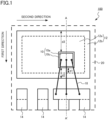
- Fig. 1 is a schematic top view of the semiconductor device of the first embodiment.
- Fig. 1 is a top view excluding a resin layer.
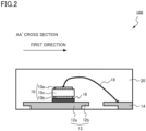
- Fig. 2 is a schematic cross-sectional view of the semiconductor device of the first embodiment.
- Fig. 2 is a cross-sectional view taken along the line AA' of Fig. 1 .
- Fig. 3 is a schematic top view of the semiconductor device of the first embodiment.
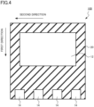
- Fig. 4 is a schematic bottom view of the semiconductor device of the first embodiment.
- the semiconductor device 100 includes a diode chip 10 (semiconductor chip), a die pad 12, a lead portion 14, a connection layer 16, a plurality of bonding wires 18, and a resin layer 20.
- the diode chip 10 includes an anode electrode 10a (upper electrode), a cathode electrode 10b (lower electrode), and a silicon carbide layer 10c.
- the die pad 12 includes a central region 12a (first region) and a peripheral region 12b (second region).
- the diode chip 10 is an example of a semiconductor chip.
- the anode electrode 10a is an example of the upper electrode.
- the cathode electrode 10b is an example of the lower electrode.
- the central region 12a is an example of the first region.
- the peripheral region 12b is an example of the second region.
- the die pad 12 has, for example, a rectangular shape.
- the die pad 12 includes the central region 12a and the peripheral region 12b.
- the peripheral region 12b surrounds the central region 12a.
- the thickness of the peripheral region 12b is smaller than the thickness of the central region 12a.
- the thickness of the central region 12a is equal to or more than 0.1 mm and equal to or less than 1 mm, for example.
- the thickness of the peripheral region 12b is equal to or less than half the thickness of the central region 12a, for example.
- the thin peripheral region 12b is provided to improve the support characteristics of the die pad 12 by the resin layer 20.
- the die pad 12 is a metal.
- the die pad 12 is, for example, copper or a copper alloy.
- the direction parallel to one side of the die pad 12 is defined as a first direction
- the direction parallel to the other side of the die pad 12 is defined as a second direction.
- the first direction is a direction parallel to the short side of the die pad 12
- the second direction is a direction parallel to the long side of the die pad 12.
- the direction in which the diode chip 10 of the die pad 12 is provided is referred to as upper, and the opposite direction is referred to as lower.
- the diode chip 10 includes the anode electrode 10a, the cathode electrode 10b, and the silicon carbide layer 10c.
- the silicon carbide layer 10c is provided between the anode electrode 10a and the cathode electrode 10b.
- the diode chip 10 is provided on the die pad 12.
- the diode chip 10 is provided on the surface of the die pad 12.
- the diode chip 10 is provided on the inner side rather than the peripheral region 12b on the surface of the die pad 12.
- the chip size of the diode chip 10 is, for example, 1 mm ⁇ 1 mm.
- the thickness of the silicon carbide layer 10c is equal to or more than 50 ⁇ m and equal to or less than 150 ⁇ m, for example.
- a first distance (d1 in Fig. 1 ) between the diode chip 10 and the peripheral region 12b in a direction parallel to the surface of the die pad 12 is equal to or more than the thickness of the silicon carbide layer 10c, for example.
- the first distance (d1 in Fig. 1 ) between the diode chip 10 and the peripheral region 12b in the first direction is equal to or more than the thickness of the silicon carbide layer 10c, for example.
- the first distance d1 is equal to or more than 50 ⁇ m, for example.
- a second distance (d2 in Fig. 1 ) between the diode chip 10 and the end of the die pad 12 in the first direction is shorter than a third distance (d3 in Fig. 1 ) between the diode chip 10 and the end of the die pad 12 in a direction opposite to the first direction, for example.
- the difference between the third distance d3 and the second distance d2 is equal to or more than the width of the diode chip 10 in the first direction, for example.
- the difference between the third distance d3 and the second distance d2 is equal to or more than three times the width of the diode chip 10 in the first direction, for example.
- the difference between the third distance d3 and the second distance d2 is equal to or more than 1 mm, for example.
- connection layer 16 is provided between the die pad 12 and the diode chip 10.
- the connection layer 16 connects the die pad 12 and the diode chip 10 to each other.
- the connection layer 16 connects the cathode electrode 10b of the diode chip 10 to the surface of the die pad 12.
- connection layer 16 is a conductor.
- the connection layer 16 contains, for example, solder.
- the connection layer 16 is, for example, a solder layer.
- connection layer 16 is equal to or more than 2 ⁇ m and equal to or less than 10 ⁇ m, for example.
- the lead portion 14 is provided in the first direction of the die pad 12.
- the lead portion 14 is not provided, for example, in a direction opposite to the first direction of the die pad 12.
- the lead portion 14 is not provided, for example, in the second direction of the die pad 12 and in a direction opposite to the second direction.
- the lead portion 14 is provided to obtain an electrical connection between the diode chip 10 and the outside of the semiconductor device 100.
- the lead portion 14 is a metal.
- the lead portion 14 is, for example, copper or a copper alloy.
- the lead portion 14 is formed of, for example, the same material as the die pad 12.
- the bonding wire 18 connects the anode electrode 10a of the diode chip 10 and the lead portion 14 to each other.
- the bonding wire 18 electrically connects the anode electrode 10a and the lead portion 14 to each other.
- the bonding wire 18 is a metal wire.
- the bonding wire 18 contains, for example, copper (Cu) or aluminum (Al).
- the bonding wire 18 is, for example, a copper wire or an aluminum wire.
- the resin layer 20 surrounds the diode chip 10 and the bonding wire 18.
- the resin layer 20 has a function of protecting the diode chip 10 and the bonding wire 18.
- the resin layer 20 contains a resin.
- the resin layer 20 contains, for example, an epoxy resin.
- a part of the die pad 12 and a part of the lead portion 14 are exposed on the bottom surface of the semiconductor device 100.
- connection portion In a semiconductor device in which a semiconductor chip is fixed on a die pad using a connection layer such as solder, high reliability is required for a connection portion using the connection layer. For example, when the semiconductor chip is peeled off at the connection portion due to temperature changes during the use of the semiconductor device, the device characteristics of the semiconductor device change, which causes a problem. For example, when the semiconductor device is a diode, if peeling occurs at the connection portion, the on-resistance of the diode increases, which causes a problem.
- the peeling of the semiconductor chip is caused by the stress generated by the difference in the coefficient of thermal expansion between the members formed of different materials, such as a semiconductor chip, a die pad, a resin layer, a solder layer, and a bonding wire.
- the semiconductor chip contains a silicon carbide layer
- the peeling of the semiconductor chip is accelerated as compared with a case where the semiconductor chip contains a silicon layer. It is thought that the reason why the peeling of the semiconductor chip is accelerated when the semiconductor chip contains the silicon carbide layer is related to the fact that the silicon carbide layer has a higher Young's modulus than the silicon layer.
- the reason why the peeling of the semiconductor chip is accelerated when the semiconductor chip contains the silicon carbide layer is related to the fact that the amount of current per chip unit area in the semiconductor chip using the silicon carbide layer is large and accordingly the amount of heat generation is large as compared with the semiconductor chip using the silicon layer.
- Fig. 5 is a schematic top view of a semiconductor device of a first comparative example of the first embodiment.
- Fig. 5 is a diagram corresponding to Fig. 1 of the first embodiment.
- the semiconductor device of the first comparative example is a semiconductor device 901.
- a diode chip containing a silicon carbide layer is packaged with resin.
- the semiconductor device 901 of the first comparative example is different from the semiconductor device 100 of the first embodiment in that a part of the diode chip 10 is provided in the peripheral region 12b of the die pad 12.
- the diode chip 10 is likely to be peeled off at the connection portion using the connection layer 16. It is thought that this is because the stress generated at the boundary between the central region 12a and the peripheral region 12b having different thicknesses increases. Therefore, it is thought that the stress applied to the connection portion between the die pad 12 and the diode chip 10 increases and accordingly, the diode chip 10 is likely to be peeled off.
- the diode chip 10 is provided on the inner side rather than the peripheral region 12b on the surface of the die pad 12. Therefore, the stress applied to the connection portion between the die pad 12 and the diode chip 10 is smaller than that in the semiconductor device 901 of the first comparative example. As a result, since the peeling of the diode chip 10 is suppressed, the reliability of the semiconductor device 100 is improved.
- the first distance (d1 in Fig. 1 ) between the diode chip 10 and the peripheral region 12b in the first direction is preferably equal to or more than the thickness of the silicon carbide layer 10c.
- the first distance d1 is preferably equal to or more than 50 ⁇ m, and more preferably equal to or more than 100 ⁇ m.
- Fig. 6 is a schematic top view of a semiconductor device of a second comparative example of the first embodiment.
- Fig. 6 is a diagram corresponding to Fig. 1 of the first embodiment.
- the semiconductor device of the second comparative example is a semiconductor device 902.
- a diode chip containing a silicon carbide layer is packaged with resin.
- the semiconductor device 902 of the second comparative example is different from the semiconductor device 100 of the first embodiment in that the second distance (d2 in Fig. 6 ) between the diode chip 10 and the end of the die pad 12 in the first direction is longer than the third distance (d3 in Fig. 6 ) between the diode chip 10 and the end of the die pad 12 in a direction opposite to the first direction.
- the stress applied to the connection portion between the die pad 12 and the diode chip 10 changes. It is considered that as the length of the bonding wire 18 increases, the stress applied to the connection portion between the die pad 12 and the diode chip 10 increases.
- the second distance (d2 in Fig. 1 ) between the diode chip 10 and the end of the die pad 12 in the first direction is shorter than the third distance (d3 in Fig. 1 ) between the diode chip 10 and the end of the die pad 12 in a direction opposite to the first direction.
- the distance between the diode chip 10 and the lead portion 14 becomes shorter than that in the semiconductor device 902 of the second comparative example.
- the length of the bonding wire 18 can be shortened. Therefore, as compared with the semiconductor device 902 of the second comparative example, the stress applied to the connection portion between the die pad 12 and the diode chip 10 due to the bonding wire 18 and the resin layer 20 surrounding the bonding wire 18 is reduced. As a result, since the peeling of the diode chip 10 is suppressed, the reliability of the semiconductor device 100 is improved.
- the difference between the third distance d3 and the second distance d2 is preferably equal to or more than the width of the diode chip 10 in the first direction. From the viewpoint of reducing the stress applied to the connection portion between the die pad 12 and the diode chip 10, the difference between the third distance d3 and the second distance d2 is preferably equal to or more than 1 mm, and more preferably equal to or more than 2 mm.
- the thickness of the connection layer 16 is preferably equal to or less than 10 ⁇ m.
- the resistance of the connection layer 16 is reduced and the amount of heat generated in the connection layer 16 is suppressed. Therefore, the stress applied to the connection portion between the die pad 12 and the diode chip 10 is reduced. As a result, since the peeling of the diode chip 10 is suppressed, the reliability of the semiconductor device 100 is improved.
- the first embodiment it is possible to realize a semiconductor device in which the peeling of a semiconductor chip is suppressed to improve the reliability.
- a semiconductor device of a second embodiment is different from the semiconductor device of the first embodiment in that the angles formed by the extension directions of a plurality of bonding wires and the first direction are equal to or less than 5°.
- the description of a part of the content overlapping the first embodiment may be omitted.
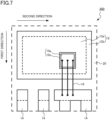
- Fig. 7 is a schematic top view of the semiconductor device of the second embodiment.
- Fig. 7 is a diagram corresponding to Fig. 1 of the first embodiment.
- the semiconductor device of the second embodiment is a semiconductor device 200.
- a diode chip containing a silicon carbide layer is packaged with resin.
- the angles formed by all the extension directions of the plurality of bonding wires 18 and the first direction are equal to or less than 5°.
- Fig. 7 illustrates a case where the angle formed by the extension direction of the bonding wire 18 and the first direction is 0°, that is, the extension direction of the bonding wire 18 and the first direction are parallel.
- angles formed by all the extension directions of the plurality of bonding wires 18 and the first direction are preferably equal to or less than 3°, more preferably equal to or less than 1°, and even more preferably 0°.
- the second embodiment it is possible to realize a semiconductor device in which the peeling of a semiconductor chip is suppressed to improve the reliability.
- a semiconductor device of a third embodiment is different from the semiconductor device of the second embodiment in that a plurality of bonding wires include a first bonding wire and a second bonding wire and a position where the first bonding wire is connected to the upper electrode and a position where the second bonding wire is connected to the upper electrode are shifted from each other in the first direction.
- a plurality of bonding wires include a first bonding wire and a second bonding wire and a position where the first bonding wire is connected to the upper electrode and a position where the second bonding wire is connected to the upper electrode are shifted from each other in the first direction.
- Fig. 8 is a schematic top view of the semiconductor device of the third embodiment.
- Fig. 8 is a diagram corresponding to Fig. 1 of the first embodiment and Fig. 7 of the second embodiment.
- the semiconductor device of the third embodiment is a semiconductor device 300.
- a diode chip containing a silicon carbide layer is packaged with resin.
- the semiconductor device 300 includes a first bonding wire 18a and a second bonding wire 18b.
- the first bonding wire 18a and the second bonding wire 18b are adjacent to each other in the second direction.
- the angles formed by all the extension directions of the first and second bonding wires 18a and 18b and the first direction is equal to or less than 5°.
- the position where the first bonding wire 18a is connected to the anode electrode 10a and the position where the second bonding wire 18b is connected to the anode electrode 10a are shifted from each other in the first direction.
- the position where the first bonding wire 18a is connected to the lead portion 14 and the position where the second bonding wire 18b is connected to the lead portion 14 are shifted from each other in the first direction.
- the semiconductor device 300 it is possible to shorten the distance between adjacent bonding wires as compared with the semiconductor device 200. Therefore, it is possible to increase the number of bonding wires for connecting the anode electrode 10a and the lead portion 14 to each other.
- the peeling of the diode chip 10 is suppressed by shortening the distance between the adjacent bonding wires to increase the number of bonding wires.
- the amount of resin layer 20 between the adjacent bonding wires is reduced. It is thought that the reduction in the amount of resin layer 20 between the adjacent bonding wires reduces the stress applied to the diode chip 10 by the bonding wires.
- the third embodiment it is possible to realize a semiconductor device in which the peeling of a semiconductor chip is suppressed to improve the reliability.
- a diode has been described as an example of the semiconductor chip.
- the semiconductor chip is not limited to the diode.
- the semiconductor chip may be a metal oxide semiconductor field effect transistor (MOSFET) or an insulated gate bipolar transistor (IGBT).
- MOSFET metal oxide semiconductor field effect transistor
- IGBT insulated gate bipolar transistor
- the number of bonding wires is 3 or 5 has been described as an example.
- the number of bonding wires can be any number.
Landscapes
- Die Bonding (AREA)
- Semiconductor Integrated Circuits (AREA)
- Structures Or Materials For Encapsulating Or Coating Semiconductor Devices Or Solid State Devices (AREA)
Abstract
A semiconductor device of embodiments includes: a die pad (12) including a first region (12a) and a second region (12b) surrounding the first region (12a) and thinner than the first region (12a); a semiconductor chip (10) including an upper electrode (10a), a lower electrode (10b), and a silicon carbide layer (10c) between the upper electrode (10a) and the lower electrode (10b) and provided on an inner side rather than the second region (12b) on a surface of the die pad (12); and a connection layer (16) for connecting the lower electrode (10) to the surface of the die pad (12).
Description
- This application is based upon and claims the benefit of priority from
Japanese Patent Application No. 2021-152687, filed on September 17, 2021 - Embodiments described herein relate generally to a semiconductor device.
- In a semiconductor device in which a semiconductor chip is fixed on a die pad using a connection layer such as solder, high reliability is required for a connection portion using the connection layer. For example, when the semiconductor chip is peeled off at the connection portion due to temperature changes during the use of the semiconductor device, the device characteristics of the semiconductor device change, which causes a problem.
-
-
Fig. 1 is a schematic top view of a semiconductor device of a first embodiment; -
Fig. 2 is a schematic cross-sectional view of the semiconductor device of the first embodiment; -
Fig. 3 is a schematic top view of the semiconductor device of the first embodiment; -
Fig. 4 is a schematic bottom view of the semiconductor device of the first embodiment; -
Fig. 5 is a schematic top view of a semiconductor device of a first comparative example of the first embodiment; -
Fig. 6 is a schematic top view of a semiconductor device of a second comparative example of the first embodiment; -
Fig. 7 is a schematic top view of a semiconductor device of a second embodiment; and -
Fig. 8 is a schematic top view of a semiconductor device of a third embodiment. - A semiconductor device of embodiments includes: a die pad including a first region and a second region surrounding the first region and thinner than the first region; a semiconductor chip including an upper electrode, a lower electrode, and a silicon carbide layer between the upper electrode and the lower electrode, the semiconductor chip provided on a surface of the die pad, and the semiconductor chip provided on an inner side rather than the second region; and a connection layer provided between the lower electrode and the surface, and the connection layer connecting the lower electrode and the surface.
- Hereinafter, embodiments will be described with reference to the diagrams. In the following description, the same or similar members and the like may be denoted by the same reference numerals, and the description of the members and the like once described may be omitted as appropriate.
- A semiconductor device of a first embodiment includes: a die pad including a first region and a second region surrounding the first region and thinner than the first region; a semiconductor chip including an upper electrode, a lower electrode, and a silicon carbide layer between the upper electrode and the lower electrode, the semiconductor chip provided on a surface of the die pad, and the semiconductor chip provided on an inner side rather than the second region; and a connection layer provided between the lower electrode and the surface, and the connection layer connecting the lower electrode and the surface.
- The semiconductor device of the first embodiment is a
semiconductor device 100 in which a diode chip including a silicon carbide layer is packaged with resin. -
Fig. 1 is a schematic top view of the semiconductor device of the first embodiment.Fig. 1 is a top view excluding a resin layer.Fig. 2 is a schematic cross-sectional view of the semiconductor device of the first embodiment.Fig. 2 is a cross-sectional view taken along the line AA' ofFig. 1 .Fig. 3 is a schematic top view of the semiconductor device of the first embodiment.Fig. 4 is a schematic bottom view of the semiconductor device of the first embodiment. - The
semiconductor device 100 includes a diode chip 10 (semiconductor chip), adie pad 12, alead portion 14, aconnection layer 16, a plurality ofbonding wires 18, and aresin layer 20. - The
diode chip 10 includes ananode electrode 10a (upper electrode), acathode electrode 10b (lower electrode), and asilicon carbide layer 10c. The diepad 12 includes acentral region 12a (first region) and aperipheral region 12b (second region). - The
diode chip 10 is an example of a semiconductor chip. Theanode electrode 10a is an example of the upper electrode. Thecathode electrode 10b is an example of the lower electrode. Thecentral region 12a is an example of the first region. Theperipheral region 12b is an example of the second region. - The die
pad 12 has, for example, a rectangular shape. The diepad 12 includes thecentral region 12a and theperipheral region 12b. Theperipheral region 12b surrounds thecentral region 12a. - As shown in
Fig. 2 , the thickness of theperipheral region 12b is smaller than the thickness of thecentral region 12a. The thickness of thecentral region 12a is equal to or more than 0.1 mm and equal to or less than 1 mm, for example. The thickness of theperipheral region 12b is equal to or less than half the thickness of thecentral region 12a, for example. - The thin
peripheral region 12b is provided to improve the support characteristics of thedie pad 12 by theresin layer 20. - The die
pad 12 is a metal. Thedie pad 12 is, for example, copper or a copper alloy. - Hereinafter, as shown in
Fig. 1 , the direction parallel to one side of thedie pad 12 is defined as a first direction, and the direction parallel to the other side of thedie pad 12 is defined as a second direction. For example, the first direction is a direction parallel to the short side of thedie pad 12, and the second direction is a direction parallel to the long side of thedie pad 12. - In addition, hereinafter, for convenience of explanation, the direction in which the
diode chip 10 of thedie pad 12 is provided is referred to as upper, and the opposite direction is referred to as lower. - The
diode chip 10 includes theanode electrode 10a, thecathode electrode 10b, and thesilicon carbide layer 10c. Thesilicon carbide layer 10c is provided between theanode electrode 10a and thecathode electrode 10b. - The
diode chip 10 is provided on the diepad 12. Thediode chip 10 is provided on the surface of the diepad 12. Thediode chip 10 is provided on the inner side rather than theperipheral region 12b on the surface of thedie pad 12. - The chip size of the
diode chip 10 is, for example, 1 mm × 1 mm. The thickness of thesilicon carbide layer 10c is equal to or more than 50 µm and equal to or less than 150 µm, for example. - A first distance (d1 in
Fig. 1 ) between thediode chip 10 and theperipheral region 12b in a direction parallel to the surface of thedie pad 12 is equal to or more than the thickness of thesilicon carbide layer 10c, for example. The first distance (d1 inFig. 1 ) between thediode chip 10 and theperipheral region 12b in the first direction is equal to or more than the thickness of thesilicon carbide layer 10c, for example. The first distance d1 is equal to or more than 50 µm, for example. - A second distance (d2 in
Fig. 1 ) between thediode chip 10 and the end of thedie pad 12 in the first direction is shorter than a third distance (d3 inFig. 1 ) between thediode chip 10 and the end of thedie pad 12 in a direction opposite to the first direction, for example. The difference between the third distance d3 and the second distance d2 is equal to or more than the width of thediode chip 10 in the first direction, for example. The difference between the third distance d3 and the second distance d2 is equal to or more than three times the width of thediode chip 10 in the first direction, for example. The difference between the third distance d3 and the second distance d2 is equal to or more than 1 mm, for example. - The
connection layer 16 is provided between thedie pad 12 and thediode chip 10. Theconnection layer 16 connects thedie pad 12 and thediode chip 10 to each other. Theconnection layer 16 connects thecathode electrode 10b of thediode chip 10 to the surface of thedie pad 12. - The
connection layer 16 is a conductor. Theconnection layer 16 contains, for example, solder. Theconnection layer 16 is, for example, a solder layer. - The thickness of the
connection layer 16 is equal to or more than 2 µm and equal to or less than 10 µm, for example. - The
lead portion 14 is provided in the first direction of thedie pad 12. Thelead portion 14 is not provided, for example, in a direction opposite to the first direction of thedie pad 12. Thelead portion 14 is not provided, for example, in the second direction of thedie pad 12 and in a direction opposite to the second direction. - The
lead portion 14 is provided to obtain an electrical connection between thediode chip 10 and the outside of thesemiconductor device 100. - The
lead portion 14 is a metal. Thelead portion 14 is, for example, copper or a copper alloy. Thelead portion 14 is formed of, for example, the same material as thedie pad 12. - The
bonding wire 18 connects theanode electrode 10a of thediode chip 10 and thelead portion 14 to each other. Thebonding wire 18 electrically connects theanode electrode 10a and thelead portion 14 to each other. - The
bonding wire 18 is a metal wire. Thebonding wire 18 contains, for example, copper (Cu) or aluminum (Al). Thebonding wire 18 is, for example, a copper wire or an aluminum wire. - The
resin layer 20 surrounds thediode chip 10 and thebonding wire 18. Theresin layer 20 has a function of protecting thediode chip 10 and thebonding wire 18. - The
resin layer 20 contains a resin. Theresin layer 20 contains, for example, an epoxy resin. - As shown in
Fig. 3 , for example, only theresin layer 20 is present on the top surface of thesemiconductor device 100. In addition, as shown inFig. 4 , for example, a part of thedie pad 12 and a part of thelead portion 14 are exposed on the bottom surface of thesemiconductor device 100. - Next, the function and effect of the semiconductor device of the first embodiment will be described.
- In a semiconductor device in which a semiconductor chip is fixed on a die pad using a connection layer such as solder, high reliability is required for a connection portion using the connection layer. For example, when the semiconductor chip is peeled off at the connection portion due to temperature changes during the use of the semiconductor device, the device characteristics of the semiconductor device change, which causes a problem. For example, when the semiconductor device is a diode, if peeling occurs at the connection portion, the on-resistance of the diode increases, which causes a problem.
- The peeling of the semiconductor chip is caused by the stress generated by the difference in the coefficient of thermal expansion between the members formed of different materials, such as a semiconductor chip, a die pad, a resin layer, a solder layer, and a bonding wire. When the semiconductor chip contains a silicon carbide layer, for example, the peeling of the semiconductor chip is accelerated as compared with a case where the semiconductor chip contains a silicon layer. It is thought that the reason why the peeling of the semiconductor chip is accelerated when the semiconductor chip contains the silicon carbide layer is related to the fact that the silicon carbide layer has a higher Young's modulus than the silicon layer. In addition, it is also thought that the reason why the peeling of the semiconductor chip is accelerated when the semiconductor chip contains the silicon carbide layer is related to the fact that the amount of current per chip unit area in the semiconductor chip using the silicon carbide layer is large and accordingly the amount of heat generation is large as compared with the semiconductor chip using the silicon layer.
-
Fig. 5 is a schematic top view of a semiconductor device of a first comparative example of the first embodiment.Fig. 5 is a diagram corresponding toFig. 1 of the first embodiment. - The semiconductor device of the first comparative example is a
semiconductor device 901. In thesemiconductor device 901, similarly to thesemiconductor device 100 of the first embodiment, a diode chip containing a silicon carbide layer is packaged with resin. - The
semiconductor device 901 of the first comparative example is different from thesemiconductor device 100 of the first embodiment in that a part of thediode chip 10 is provided in theperipheral region 12b of thedie pad 12. - In the
semiconductor device 901, thediode chip 10 is likely to be peeled off at the connection portion using theconnection layer 16. It is thought that this is because the stress generated at the boundary between thecentral region 12a and theperipheral region 12b having different thicknesses increases. Therefore, it is thought that the stress applied to the connection portion between thedie pad 12 and thediode chip 10 increases and accordingly, thediode chip 10 is likely to be peeled off. - In the
semiconductor device 100 of the first embodiment, thediode chip 10 is provided on the inner side rather than theperipheral region 12b on the surface of thedie pad 12. Therefore, the stress applied to the connection portion between thedie pad 12 and thediode chip 10 is smaller than that in thesemiconductor device 901 of the first comparative example. As a result, since the peeling of thediode chip 10 is suppressed, the reliability of thesemiconductor device 100 is improved. - From the viewpoint of reducing the stress applied to the connection portion between the
die pad 12 and thediode chip 10, the first distance (d1 inFig. 1 ) between thediode chip 10 and theperipheral region 12b in the first direction is preferably equal to or more than the thickness of thesilicon carbide layer 10c. In addition, from the viewpoint of reducing the stress applied to the connection portion between thedie pad 12 and thediode chip 10, the first distance d1 is preferably equal to or more than 50 µm, and more preferably equal to or more than 100 µm. -
Fig. 6 is a schematic top view of a semiconductor device of a second comparative example of the first embodiment.Fig. 6 is a diagram corresponding toFig. 1 of the first embodiment. - The semiconductor device of the second comparative example is a
semiconductor device 902. In thesemiconductor device 902, similarly to thesemiconductor device 100 of the first embodiment, a diode chip containing a silicon carbide layer is packaged with resin. - The
semiconductor device 902 of the second comparative example is different from thesemiconductor device 100 of the first embodiment in that the second distance (d2 inFig. 6 ) between thediode chip 10 and the end of thedie pad 12 in the first direction is longer than the third distance (d3 inFig. 6 ) between thediode chip 10 and the end of thedie pad 12 in a direction opposite to the first direction. - Due to the shrinkage or expansion of the
bonding wire 18 and theresin layer 20 surrounding thebonding wire 18, the stress applied to the connection portion between thedie pad 12 and thediode chip 10 changes. It is considered that as the length of thebonding wire 18 increases, the stress applied to the connection portion between thedie pad 12 and thediode chip 10 increases. - In the
semiconductor device 100, the second distance (d2 inFig. 1 ) between thediode chip 10 and the end of thedie pad 12 in the first direction is shorter than the third distance (d3 inFig. 1 ) between thediode chip 10 and the end of thedie pad 12 in a direction opposite to the first direction. - By making the second distance d2 shorter than the third distance d3, the distance between the
diode chip 10 and thelead portion 14 becomes shorter than that in thesemiconductor device 902 of the second comparative example. By shortening the distance between thediode chip 10 and thelead portion 14, the length of thebonding wire 18 can be shortened. Therefore, as compared with thesemiconductor device 902 of the second comparative example, the stress applied to the connection portion between thedie pad 12 and thediode chip 10 due to thebonding wire 18 and theresin layer 20 surrounding thebonding wire 18 is reduced. As a result, since the peeling of thediode chip 10 is suppressed, the reliability of thesemiconductor device 100 is improved. - From the viewpoint of reducing the stress applied to the connection portion between the
die pad 12 and thediode chip 10, the difference between the third distance d3 and the second distance d2 is preferably equal to or more than the width of thediode chip 10 in the first direction. From the viewpoint of reducing the stress applied to the connection portion between thedie pad 12 and thediode chip 10, the difference between the third distance d3 and the second distance d2 is preferably equal to or more than 1 mm, and more preferably equal to or more than 2 mm. - In the
semiconductor device 100, the thickness of theconnection layer 16 is preferably equal to or less than 10 µm. By setting the thickness of theconnection layer 16 to be equal to or less than 10 µm, the resistance of theconnection layer 16 is reduced and the amount of heat generated in theconnection layer 16 is suppressed. Therefore, the stress applied to the connection portion between thedie pad 12 and thediode chip 10 is reduced. As a result, since the peeling of thediode chip 10 is suppressed, the reliability of thesemiconductor device 100 is improved. - As described above, according to the first embodiment, it is possible to realize a semiconductor device in which the peeling of a semiconductor chip is suppressed to improve the reliability.
- A semiconductor device of a second embodiment is different from the semiconductor device of the first embodiment in that the angles formed by the extension directions of a plurality of bonding wires and the first direction are equal to or less than 5°. Hereinafter, the description of a part of the content overlapping the first embodiment may be omitted.
-
Fig. 7 is a schematic top view of the semiconductor device of the second embodiment.Fig. 7 is a diagram corresponding toFig. 1 of the first embodiment. - The semiconductor device of the second embodiment is a
semiconductor device 200. In thesemiconductor device 200, similarly to thesemiconductor device 100 of the first embodiment, a diode chip containing a silicon carbide layer is packaged with resin. - In the
semiconductor device 200, the angles formed by all the extension directions of the plurality ofbonding wires 18 and the first direction are equal to or less than 5°.Fig. 7 illustrates a case where the angle formed by the extension direction of thebonding wire 18 and the first direction is 0°, that is, the extension direction of thebonding wire 18 and the first direction are parallel. - As a result of the study by the inventors, it was confirmed that the peeling of the
diode chip 10 was suppressed by setting the angle formed by the extension direction of thebonding wire 18 and the first direction to be equal to or less than 5°. Although the cause is not necessarily clear, it is thought that this is due to the effect that the direction of the stress applied to thediode chip 10 is limited to the first direction by the plurality ofbonding wires 18. - From the viewpoint of suppressing the peeling of the
diode chip 10, the angles formed by all the extension directions of the plurality ofbonding wires 18 and the first direction are preferably equal to or less than 3°, more preferably equal to or less than 1°, and even more preferably 0°. - As described above, according to the second embodiment, it is possible to realize a semiconductor device in which the peeling of a semiconductor chip is suppressed to improve the reliability.
- A semiconductor device of a third embodiment is different from the semiconductor device of the second embodiment in that a plurality of bonding wires include a first bonding wire and a second bonding wire and a position where the first bonding wire is connected to the upper electrode and a position where the second bonding wire is connected to the upper electrode are shifted from each other in the first direction. Hereinafter, the description of a part of the content overlapping the first and second embodiments may be omitted.
-
Fig. 8 is a schematic top view of the semiconductor device of the third embodiment.Fig. 8 is a diagram corresponding toFig. 1 of the first embodiment andFig. 7 of the second embodiment. - The semiconductor device of the third embodiment is a
semiconductor device 300. In thesemiconductor device 300, similarly to thesemiconductor device 100 of the first embodiment, a diode chip containing a silicon carbide layer is packaged with resin. - The
semiconductor device 300 includes afirst bonding wire 18a and asecond bonding wire 18b. Thefirst bonding wire 18a and thesecond bonding wire 18b are adjacent to each other in the second direction. The angles formed by all the extension directions of the first andsecond bonding wires - The position where the
first bonding wire 18a is connected to theanode electrode 10a and the position where thesecond bonding wire 18b is connected to theanode electrode 10a are shifted from each other in the first direction. In addition, the position where thefirst bonding wire 18a is connected to thelead portion 14 and the position where thesecond bonding wire 18b is connected to thelead portion 14 are shifted from each other in the first direction. - With the above-described configuration, in the
semiconductor device 300, it is possible to shorten the distance between adjacent bonding wires as compared with thesemiconductor device 200. Therefore, it is possible to increase the number of bonding wires for connecting theanode electrode 10a and thelead portion 14 to each other. - In the
semiconductor device 300, the peeling of thediode chip 10 is suppressed by shortening the distance between the adjacent bonding wires to increase the number of bonding wires. By shortening the distance between the first andsecond bonding wires resin layer 20 between the adjacent bonding wires is reduced. It is thought that the reduction in the amount ofresin layer 20 between the adjacent bonding wires reduces the stress applied to thediode chip 10 by the bonding wires. - As described above, according to the third embodiment, it is possible to realize a semiconductor device in which the peeling of a semiconductor chip is suppressed to improve the reliability.
- In the first to third embodiments, a diode has been described as an example of the semiconductor chip.
- However, the semiconductor chip is not limited to the diode. For example, the semiconductor chip may be a metal oxide semiconductor field effect transistor (MOSFET) or an insulated gate bipolar transistor (IGBT).
- In the first to third embodiments, the case where the number of bonding wires is 3 or 5 has been described as an example. However, the number of bonding wires can be any number.
- While certain embodiments have been described, these embodiments have been presented by way of example only, and are not intended to limit the scope of the inventions. Indeed, the semiconductor device described herein may be embodied in a variety of other forms; furthermore, various omissions, substitutions and changes in the form of the devices and methods described herein may be made without departing from the spirit of the inventions. The accompanying claims and their equivalents are intended to cover such forms or modifications as would fall within the scope and spirit of the inventions.
- It is explicitly stated that all features disclosed in the description and/or the claims are intended to be disclosed separately and independently from each other for the purpose of original disclosure as well as for the purpose of restricting the claimed invention independent of the composition of the features in the embodiments and/or the claims. It is explicitly stated that all value ranges or indications of groups of entities disclose every possible intermediate value or intermediate entity for the purpose of original disclosure as well as for the purpose of restricting the claimed invention, in particular as limits of value ranges.
Claims (10)
- A semiconductor device (100), comprising:a die pad (12) including a first region (12a) and a second region (12b) surrounding the first region (12a) and thinner than the first region (12a);a semiconductor chip (10) including an upper electrode (10a), a lower electrode (10b), and a silicon carbide layer (10c) between the upper electrode (10a) and the lower electrode (10b), the semiconductor chip (10) provided on a surface of the die pad (12), and the semiconductor chip (10) provided on an inner side rather than the second region (12b); anda connection layer (16) provided between the lower electrode (10b) and the surface, and the connection layer (16) connecting the lower electrode (12b) and the surface.
- The semiconductor device (100) according to claim 1, further comprising:a lead portion (14) provided in a first direction of the die pad (12);a plurality of bonding wires (18) connecting the upper electrode (10a) and the lead portion (14) to each other; anda resin layer (20) surrounding the semiconductor chip (10) and the plurality of bonding wires (18).
- The semiconductor device (100) according to claim 1,
wherein a first distance (d1) between the semiconductor chip (10) and the second region (12b) in a direction parallel to the surface is equal to or more than a thickness of the silicon carbide layer (12c). - The semiconductor device (100) according to claim 2,
wherein a second distance (d2) between the semiconductor chip (10) and an end of the die pad (12) in the first direction is shorter than a third distance (d3) between the semiconductor chip (10) and an end of the die pad (12) in a direction opposite to the first direction. - The semiconductor device (100) according to claim 4,
wherein a difference between the third distance (d3) and the second distance (d2) is equal to or more than a width of the semiconductor chip (10) in the first direction. - The semiconductor device (100) according to claim 1,
wherein a thickness of the connection layer (16) is equal to or less than 10 µm. - The semiconductor device (100) according to claim 2,
wherein an angle formed by an extension direction of each of the plurality of bonding wires (18) and the first direction is equal to or less than 5°. - The semiconductor device (100) according to claim 7,wherein the plurality of bonding wires (18) include a first bonding wire (18a) and a second bonding wire (18b), anda position where the first bonding wire (18a) is connected to the upper electrode (10a) and a position where the second bonding wire (18b) is connected to the upper electrode (10a) are shifted from each other in the first direction.
- The semiconductor device (100) according to claim 1,
wherein the semiconductor chip (10) is a diode chip. - The semiconductor device (100) according to claim 1,
wherein the connection layer (16) is a solder layer.
Applications Claiming Priority (1)
| Application Number | Priority Date | Filing Date | Title |
|---|---|---|---|
| JP2021152687A JP7631157B2 (en) | 2021-09-17 | 2021-09-17 | Semiconductor Device |
Publications (1)
| Publication Number | Publication Date |
|---|---|
| EP4152378A1 true EP4152378A1 (en) | 2023-03-22 |
Family
ID=80448627
Family Applications (1)
| Application Number | Title | Priority Date | Filing Date |
|---|---|---|---|
| EP22158420.4A Pending EP4152378A1 (en) | 2021-09-17 | 2022-02-24 | Semiconductor device |
Country Status (4)
| Country | Link |
|---|---|
| US (1) | US12341122B2 (en) |
| EP (1) | EP4152378A1 (en) |
| JP (1) | JP7631157B2 (en) |
| CN (1) | CN115831903A (en) |
Citations (3)
| Publication number | Priority date | Publication date | Assignee | Title |
|---|---|---|---|---|
| US20050035434A1 (en) * | 2003-08-14 | 2005-02-17 | Sergio Fissore | Module for EPAS/EHPAS applications |
| US20200350235A1 (en) * | 2017-11-27 | 2020-11-05 | Sumitomo Electric Industries, Ltd. | Semiconductor apparatus |
| WO2020235410A1 (en) * | 2019-05-20 | 2020-11-26 | ローム株式会社 | Semiconductor device |
Family Cites Families (27)
| Publication number | Priority date | Publication date | Assignee | Title |
|---|---|---|---|---|
| EP0878025B1 (en) * | 1996-11-05 | 2004-04-14 | Koninklijke Philips Electronics N.V. | Semiconductor device with a high-frequency bipolar transistor on an insulating substrate |
| JP2971449B2 (en) * | 1997-07-31 | 1999-11-08 | 松下電子工業株式会社 | Semiconductor device, manufacturing method thereof, and lead frame of semiconductor device |
| JP4248953B2 (en) * | 2003-06-30 | 2009-04-02 | 株式会社ルネサステクノロジ | Semiconductor device and manufacturing method thereof |
| US20080116553A1 (en) * | 2006-11-20 | 2008-05-22 | International Business Machines Corporation | Wirebond Package Design for High Speed Data Rates |
| JP2009277949A (en) | 2008-05-16 | 2009-11-26 | Panasonic Corp | Semiconductor device and method of manufacturing the same |
| JP2010147162A (en) | 2008-12-17 | 2010-07-01 | Renesas Technology Corp | Semiconductor device |
| JP2010165992A (en) * | 2009-01-19 | 2010-07-29 | Renesas Electronics Corp | Semiconductor device and method for manufacturing the same |
| JP5947165B2 (en) | 2012-09-05 | 2016-07-06 | ルネサスエレクトロニクス株式会社 | Electronic equipment |
| JP5975911B2 (en) * | 2013-03-15 | 2016-08-23 | ルネサスエレクトロニクス株式会社 | Semiconductor device |
| JP6080305B2 (en) | 2013-08-21 | 2017-02-15 | 新電元工業株式会社 | Semiconductor device manufacturing method, semiconductor device, and lead frame |
| TWI538762B (en) * | 2014-01-03 | 2016-06-21 | 樂金股份有限公司 | Solder ball bump and package structure and method of forming same |
| JP6338937B2 (en) * | 2014-06-13 | 2018-06-06 | ローム株式会社 | Power module and manufacturing method thereof |
| WO2016129097A1 (en) * | 2015-02-13 | 2016-08-18 | 株式会社日産アーク | Half-bridge power semiconductor module, and method for manufacturing same |
| JP2016040839A (en) | 2015-10-27 | 2016-03-24 | ルネサスエレクトロニクス株式会社 | Method of manufacturing semiconductor device |
| WO2017144599A1 (en) * | 2016-02-24 | 2017-08-31 | Abb Schweiz Ag | Power module based on multi-layer circuit board |
| WO2018207856A1 (en) * | 2017-05-10 | 2018-11-15 | ローム株式会社 | Power semiconductor device and method for producing same |
| JP6917010B2 (en) * | 2017-09-06 | 2021-08-11 | 大日本印刷株式会社 | Semiconductor devices and their manufacturing methods |
| DE212018000087U1 (en) * | 2017-11-20 | 2019-05-10 | Rohm Co., Ltd. | Semiconductor device |
| DE102018204376B4 (en) * | 2018-03-22 | 2022-07-07 | Infineon Technologies Ag | Silicon carbide devices and methods of making the same |
| JP2019192764A (en) * | 2018-04-24 | 2019-10-31 | 株式会社東芝 | Semiconductor device and drive circuit |
| JP2020004784A (en) * | 2018-06-26 | 2020-01-09 | 三菱電機株式会社 | Power module and power converter |
| US11227817B2 (en) * | 2018-12-12 | 2022-01-18 | Stmicroelectronics, Inc. | Compact leadframe package |
| JP7400293B2 (en) | 2019-06-21 | 2023-12-19 | 富士電機株式会社 | Semiconductor device and semiconductor device manufacturing method |
| JP7380071B2 (en) * | 2019-10-21 | 2023-11-15 | 富士電機株式会社 | semiconductor equipment |
| JP7442333B2 (en) * | 2020-02-12 | 2024-03-04 | エイブリック株式会社 | Semiconductor device and its manufacturing method |
| JP7636186B2 (en) * | 2021-02-02 | 2025-02-26 | ローム株式会社 | Semiconductor device and inspection method |
| CN117897814A (en) * | 2021-08-30 | 2024-04-16 | 罗姆股份有限公司 | Signal transmission device and insulation chip |
-
2021
- 2021-09-17 JP JP2021152687A patent/JP7631157B2/en active Active
- 2021-12-23 CN CN202111587427.2A patent/CN115831903A/en active Pending
-
2022
- 2022-02-17 US US17/674,622 patent/US12341122B2/en active Active
- 2022-02-24 EP EP22158420.4A patent/EP4152378A1/en active Pending
Patent Citations (3)
| Publication number | Priority date | Publication date | Assignee | Title |
|---|---|---|---|---|
| US20050035434A1 (en) * | 2003-08-14 | 2005-02-17 | Sergio Fissore | Module for EPAS/EHPAS applications |
| US20200350235A1 (en) * | 2017-11-27 | 2020-11-05 | Sumitomo Electric Industries, Ltd. | Semiconductor apparatus |
| WO2020235410A1 (en) * | 2019-05-20 | 2020-11-26 | ローム株式会社 | Semiconductor device |
Also Published As
| Publication number | Publication date |
|---|---|
| JP2023044582A (en) | 2023-03-30 |
| CN115831903A (en) | 2023-03-21 |
| JP7631157B2 (en) | 2025-02-18 |
| US20230091217A1 (en) | 2023-03-23 |
| US12341122B2 (en) | 2025-06-24 |
Similar Documents
| Publication | Publication Date | Title |
|---|---|---|
| US7084491B2 (en) | Semiconductor device | |
| JP7419781B2 (en) | semiconductor module | |
| US12191223B2 (en) | Semiconductor device with a supporting member and bonded metal layers | |
| JP7047895B2 (en) | Semiconductor device | |
| US20180053737A1 (en) | Power semiconductor device | |
| JP5343982B2 (en) | Semiconductor device | |
| JP6455335B2 (en) | Semiconductor device | |
| US20220077022A1 (en) | Semiconductor device | |
| US11923266B2 (en) | Semiconductor module circuit structure | |
| US11705438B2 (en) | Semiconductor device | |
| US10957673B2 (en) | Semiconductor device | |
| US11688711B2 (en) | Semiconductor device having second connector that overlaps a part of first connector | |
| US11081412B2 (en) | Semiconductor device | |
| US12341122B2 (en) | Semiconductor device | |
| JP2017135144A (en) | Semiconductor module | |
| US11749620B2 (en) | Semiconductor module | |
| US20240258188A1 (en) | Semiconductor device | |
| WO2021200543A1 (en) | Transistor and semiconductor device | |
| KR102927828B1 (en) | Semiconductor device | |
| US20250357412A1 (en) | Semiconductor device and method for manufacturing the same | |
| US20260068748A1 (en) | Semiconductor device | |
| JP5758816B2 (en) | Power semiconductor device | |
| US20240014106A1 (en) | Semiconductor device | |
| US20220148945A1 (en) | Leadframe, semiconductor device, and method for manufacturing semiconductor device | |
| JP2026081833A (en) | Semiconductor equipment |
Legal Events
| Date | Code | Title | Description |
|---|---|---|---|
| PUAI | Public reference made under article 153(3) epc to a published international application that has entered the european phase |
Free format text: ORIGINAL CODE: 0009012 |
|
| STAA | Information on the status of an ep patent application or granted ep patent |
Free format text: STATUS: REQUEST FOR EXAMINATION WAS MADE |
|
| 17P | Request for examination filed |
Effective date: 20220224 |
|
| AK | Designated contracting states |
Kind code of ref document: A1 Designated state(s): AL AT BE BG CH CY CZ DE DK EE ES FI FR GB GR HR HU IE IS IT LI LT LU LV MC MK MT NL NO PL PT RO RS SE SI SK SM TR |
|
| STAA | Information on the status of an ep patent application or granted ep patent |
Free format text: STATUS: EXAMINATION IS IN PROGRESS |
|
| 17Q | First examination report despatched |
Effective date: 20240722 |