EP4152364A1 - Electronic device and manufacturing method thereof - Google Patents
Electronic device and manufacturing method thereof Download PDFInfo
- Publication number
- EP4152364A1 EP4152364A1 EP22191114.2A EP22191114A EP4152364A1 EP 4152364 A1 EP4152364 A1 EP 4152364A1 EP 22191114 A EP22191114 A EP 22191114A EP 4152364 A1 EP4152364 A1 EP 4152364A1
- Authority
- EP
- European Patent Office
- Prior art keywords
- insulating layer
- layer
- opening
- metal layer
- metal
- Prior art date
- Legal status (The legal status is an assumption and is not a legal conclusion. Google has not performed a legal analysis and makes no representation as to the accuracy of the status listed.)
- Withdrawn
Links
Images





Classifications
-
- H—ELECTRICITY
- H10—SEMICONDUCTOR DEVICES; ELECTRIC SOLID-STATE DEVICES NOT OTHERWISE PROVIDED FOR
- H10W—GENERIC PACKAGES, INTERCONNECTIONS, CONNECTORS OR OTHER CONSTRUCTIONAL DETAILS OF DEVICES COVERED BY CLASS H10
- H10W72/00—Interconnections or connectors in packages
- H10W72/90—Bond pads, in general
-
- H—ELECTRICITY
- H10—SEMICONDUCTOR DEVICES; ELECTRIC SOLID-STATE DEVICES NOT OTHERWISE PROVIDED FOR
- H10W—GENERIC PACKAGES, INTERCONNECTIONS, CONNECTORS OR OTHER CONSTRUCTIONAL DETAILS OF DEVICES COVERED BY CLASS H10
- H10W70/00—Package substrates; Interposers; Redistribution layers [RDL]
- H10W70/60—Insulating or insulated package substrates; Interposers; Redistribution layers
- H10W70/611—Insulating or insulated package substrates; Interposers; Redistribution layers for connecting multiple chips together
-
- H—ELECTRICITY
- H10—SEMICONDUCTOR DEVICES; ELECTRIC SOLID-STATE DEVICES NOT OTHERWISE PROVIDED FOR
- H10W—GENERIC PACKAGES, INTERCONNECTIONS, CONNECTORS OR OTHER CONSTRUCTIONAL DETAILS OF DEVICES COVERED BY CLASS H10
- H10W70/00—Package substrates; Interposers; Redistribution layers [RDL]
- H10W70/01—Manufacture or treatment
- H10W70/05—Manufacture or treatment of insulating or insulated package substrates, or of interposers, or of redistribution layers
-
- H—ELECTRICITY
- H10—SEMICONDUCTOR DEVICES; ELECTRIC SOLID-STATE DEVICES NOT OTHERWISE PROVIDED FOR
- H10W—GENERIC PACKAGES, INTERCONNECTIONS, CONNECTORS OR OTHER CONSTRUCTIONAL DETAILS OF DEVICES COVERED BY CLASS H10
- H10W70/00—Package substrates; Interposers; Redistribution layers [RDL]
- H10W70/60—Insulating or insulated package substrates; Interposers; Redistribution layers
-
- H—ELECTRICITY
- H10—SEMICONDUCTOR DEVICES; ELECTRIC SOLID-STATE DEVICES NOT OTHERWISE PROVIDED FOR
- H10W—GENERIC PACKAGES, INTERCONNECTIONS, CONNECTORS OR OTHER CONSTRUCTIONAL DETAILS OF DEVICES COVERED BY CLASS H10
- H10W70/00—Package substrates; Interposers; Redistribution layers [RDL]
- H10W70/60—Insulating or insulated package substrates; Interposers; Redistribution layers
- H10W70/62—Insulating or insulated package substrates; Interposers; Redistribution layers characterised by their interconnections
- H10W70/65—Shapes or dispositions of interconnections
-
- H—ELECTRICITY
- H10—SEMICONDUCTOR DEVICES; ELECTRIC SOLID-STATE DEVICES NOT OTHERWISE PROVIDED FOR
- H10W—GENERIC PACKAGES, INTERCONNECTIONS, CONNECTORS OR OTHER CONSTRUCTIONAL DETAILS OF DEVICES COVERED BY CLASS H10
- H10W70/00—Package substrates; Interposers; Redistribution layers [RDL]
- H10W70/60—Insulating or insulated package substrates; Interposers; Redistribution layers
- H10W70/62—Insulating or insulated package substrates; Interposers; Redistribution layers characterised by their interconnections
- H10W70/65—Shapes or dispositions of interconnections
- H10W70/652—Cross-sectional shapes
-
- H—ELECTRICITY
- H10—SEMICONDUCTOR DEVICES; ELECTRIC SOLID-STATE DEVICES NOT OTHERWISE PROVIDED FOR
- H10W—GENERIC PACKAGES, INTERCONNECTIONS, CONNECTORS OR OTHER CONSTRUCTIONAL DETAILS OF DEVICES COVERED BY CLASS H10
- H10W70/00—Package substrates; Interposers; Redistribution layers [RDL]
- H10W70/60—Insulating or insulated package substrates; Interposers; Redistribution layers
- H10W70/62—Insulating or insulated package substrates; Interposers; Redistribution layers characterised by their interconnections
- H10W70/65—Shapes or dispositions of interconnections
- H10W70/654—Top-view layouts
- H10W70/655—Fan-out layouts
-
- H—ELECTRICITY
- H10—SEMICONDUCTOR DEVICES; ELECTRIC SOLID-STATE DEVICES NOT OTHERWISE PROVIDED FOR
- H10W—GENERIC PACKAGES, INTERCONNECTIONS, CONNECTORS OR OTHER CONSTRUCTIONAL DETAILS OF DEVICES COVERED BY CLASS H10
- H10W70/00—Package substrates; Interposers; Redistribution layers [RDL]
- H10W70/60—Insulating or insulated package substrates; Interposers; Redistribution layers
- H10W70/67—Insulating or insulated package substrates; Interposers; Redistribution layers characterised by their insulating layers or insulating parts
- H10W70/68—Shapes or dispositions thereof
- H10W70/685—Shapes or dispositions thereof comprising multiple insulating layers
-
- H—ELECTRICITY
- H10—SEMICONDUCTOR DEVICES; ELECTRIC SOLID-STATE DEVICES NOT OTHERWISE PROVIDED FOR
- H10W—GENERIC PACKAGES, INTERCONNECTIONS, CONNECTORS OR OTHER CONSTRUCTIONAL DETAILS OF DEVICES COVERED BY CLASS H10
- H10W72/00—Interconnections or connectors in packages
- H10W72/01—Manufacture or treatment
- H10W72/019—Manufacture or treatment of bond pads
Definitions
- the present disclosure relates to an electronic device and a manufacturing method thereof, and more particularly to an electronic device and a manufacturing method thereof that improves the adhesion between a metal layer and an insulating layer.
- the design and quality of metal traces between the components will affect the reliability of the electronic devices.
- the metal layer and the insulating layer have different material properties, so that the adhesion between the metal layer and the insulating layer is poor, thereby reducing the reliability of the electronic device. Therefore, how to improve the metal trace quality is an issue that needs further improvement.
- a second insulating layer may be formed between a first insulating layer and a seed layer, where the second insulating layer includes a silane coupling agent that enhances the adhesion between the seed layer (or the metal layer) and the first insulating layer, and a plasma surface treatment and a vacuum equipment may not be required.
- the reliability of the electronic devices can be improved, and the cost thereof can also be saved.
- the electronic device includes a first metal layer, a first insulating layer, a second metal layer and a second insulating layer.
- the first insulating layer is disposed on the first metal layer
- the second metal layer is disposed on the first insulating layer
- the second insulating layer is disposed between the second metal layer and the first insulating layer.
- the second metal layer is electrically connected to the first metal layer through a first opening of the first insulating layer and a second opening of the second insulating layer.
- the manufacturing method includes following steps. Forming a first metal layer on a substrate. Forming a first insulating layer on the substrate and the first metal layer, the first insulating layer includes a first opening, and the first opening exposes an upper surface of the first metal layer. Forming a second insulating layer on the first insulating layer, the second insulating layer extends into the first opening, the second insulating layer includes a second opening, and the second opening is disposed in the first opening. Forming a seed layer on the second insulating layer, and the seed layer extends into the second opening. Forming a second metal layer on the seed layer, and the second metal layer is electrically connected to the first metal layer through the first opening of the first insulating layer and the second opening of the second insulating layer.
- An electrical connection may be a direct connection or an indirect connection.
- the electrical signals may be transmitted by direct contact, and there are no other elements presented between the two elements.
- the electrical signals may be transmitted through the intermediate element bridging the two elements.
- the electrical connection may also be referred to as coupling.
- the width, thickness, height or area of each component, or the distance or spacing between components may be measured by using an optical microscopy (OM), a scanning electron microscope (SEM), a film thickness profile measuring instrument (a-step), an ellipsometer, or other suitable methods.
- OM optical microscopy
- SEM scanning electron microscope
- a-step film thickness profile measuring instrument
- ellipsometer an ellipsometer
- a scanning electron microscope may be used to obtain a cross-sectional structure image containing the components to be measured, and to measure the width, thickness, height or area of each component, or the distance or spacing between the components, and to obtain the volume of the component through appropriate methods (such as integration).
- the terms “about”, “equal to”, “equal” or “the same”, “substantially” or “approximately” usually mean within 20% of a given value, or within 10%, 5%, 3%, 2%, 1% or 0.5% of the given value.
- the electronic devices of the present disclosure may include, for example, a package component, a display device, an antenna device, a touch display device, a curved display device, or a non-rectangular display device (free shaped display device), but not limited thereto.
- the electronic devices may be bendable or flexible electronic devices.
- the electronic devices may include, for example, a light-emitting diode (LED), liquid crystal, fluorescence, phosphor, other suitable display medium, or a combination thereof, but not limited thereto.
- LED light-emitting diode
- the light-emitting diode may include, for example, an organic light-emitting diode (OLED), an inorganic light-emitting diode (LED), a mini light emitting diode (mini-LED), a micro light emitting diode (micro-LED) or quantum dots (QDs) light emitting diode (such as QLED, QDLED), other suitable materials, or any combination thereof, but not limited thereto.
- the display devices may include, for example, a tiled display device, but not limited thereto.
- the antenna device may include, for example, a liquid crystal antenna, or other kinds of antenna, but not limited thereto.
- the antenna device may include, for example, a tiled antenna device, but not limited thereto.
- the electronic devices of the present disclosure may be any combination of the aforementioned devices, but not limited thereto.
- the appearance of the electronic devices may be rectangular, circular, polygonal, a shape with curved edges, or other suitable shapes.
- the electronic devices may have peripheral systems such as a driving system, a control system, a light source system, a shelf system, etc., to support a display device, an antenna device or a tiled device.
- the following electronic devices take a package component as an example, but not limited thereto.
- An electronic device 10 of the present disclosure may for example be a package component, where the electronic device 10 may include a plurality of insulating layers and a plurality of metal layers, and these insulating layers and these metal layers may for example form a redistribution layer (RDL) in the package component, but not limited thereto.
- RDL redistribution layer
- the electronic device 10 may be formed of insulating layers and conductive layers stacked alternately one by one along the direction Z.
- the direction Z may be the stacking direction of the insulating layers and the metal layers in the electronic device 10, but not limited thereto.
- the direction X may be, for example, the extending direction of the insulating layer, but not limited thereto.
- the direction Z may be perpendicular to the direction X.
- the direction Z may also be referred to as a vertical projection direction or a top-view direction. The spatial relationship of the structure may be described according to the direction X and the direction Z in the following drawings.
- FIG. 1 to FIG. 6 are schematic cross-sectional diagrams illustrating a manufacturing method of an electronic device according to a first embodiment of the present disclosure
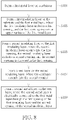
- FIG. 8 is a flow chart of steps of the manufacturing method of the electronic device according to the first embodiment of the present disclosure.
- a step S101 may be performed to form a first metal layer (such as a metal layer 1061) on a substrate 100.
- the substrate 100 may be provided, and the material of the substrate 100 may include glass, quartz, sapphire, polymers (such as polyimide (PI), polyethylene terephthalate (PET)) and/or other suitable materials to be used as a flexible substrate or a rigid substrate, but not limited thereto.
- the material of the substrate 100 may include glass, quartz, sapphire, polymers (such as polyimide (PI), polyethylene terephthalate (PET)) and/or other suitable materials to be used as a flexible substrate or a rigid substrate, but not limited thereto.
- PI polyimide
- PET polyethylene terephthalate
- a release layer 102 may be formed on the substrate 100, and a seed layer 104 may be formed on the release layer 102.
- the release layer 102 may be fully formed on the substrate 100, and the seed layer 104 may be fully formed on the release layer 102, but not limited thereto.
- the material of the release layer 102 may include silicon oxide (SiO x ), silicon nitride (SiN x ), silicon oxynitride (SiO x N y ), polymers (such as resin, epoxy resin, acrylic acid, polyimide, polyethylene terephthalate (PET)) or other suitable materials, but not limited thereto.
- the material of the seed layer 104 may include copper, titanium, aluminum, nickel, molybdenum, a combination thereof, or other suitable metal materials, but not limited thereto.
- the seed layer 104 (or the seed layers mentioned below) may be formed by electroplating or other suitable processes, but not limited thereto.
- a metal layer 1061 (or may be referred to as a first metal layer) may be formed on the seed layer 104. As shown in FIG. 1 , a metal layer 1063 may also be formed together with the metal layer 1061, but not limited thereto. In some embodiments, the metal layer 1063 and the metal layer 1061 may be formed separately, but not limited thereto. The metal layer 1061 and the metal layer 1063 may be a patterned metal layer.
- a metal layer may be formed over the entire surface of the seed layer 104, and the metal layer (or the metal layers mentioned below) may be formed by electroplating, physical vapor deposition (PVD), atomic layer deposition (ALD), metal organic chemical vapor deposition (MOCVD) or other suitable processes, but not limited thereto. Then, the metal layer 1061 and the metal layer 1063 may be formed by photolithography and etching processes, or the metal layer 1061 and the metal layer 1063 may be formed by removing unnecessary metal portions through laser, but not limited thereto. In some embodiments, the metal layer 1061 and the metal layer 1063 may be formed by a screen printing process, but not limited thereto.
- the material of the metal layer 1061 and the metal layer 1063 may include copper (Cu), titanium (Ti), aluminum (Al), nickel (Ni), molybdenum (Mo), a combination thereof, an alloy thereof, a combination of alloys of the aforementioned metals, or other suitable metal materials, but not limited thereto.
- a step S103 may be performed to form an insulating layer 110 (or may be referred to as a first insulating layer) on the substrate 100 and the first metal layer (such as the metal layer 1061), where the insulating layer 110 includes a first opening (such as an opening OP11), and the first opening exposes an upper surface (such as an upper surface 1081) of the first metal layer.
- the material of the insulating layer 110 may include organic or inorganic insulating materials, but not limited thereto. In some embodiments, the material of the insulating layer 110 (or the insulating layers mentioned below) may include an organic insulating material, such as polyimide, but not limited thereto.
- the material of the insulating layer 110 may include an inorganic insulating material, such as silicon oxide (SiO x ), silicon nitride (SiN x ) or silicon oxynitride (SiO x N y ), but not limited thereto.
- an inorganic insulating material such as silicon oxide (SiO x ), silicon nitride (SiN x ) or silicon oxynitride (SiO x N y ), but not limited thereto.
- an unpatterned insulating layer may be fully formed on the seed layer 104, the metal layer 1061 and the metal layer 1063, and the unpatterned insulating layer may be formed by a suitable coating process, laminating process, physical vapor deposition (PVD), atomic layer deposition (ALD) or other suitable thin film deposition processes, but not limited thereto.
- an opening OP11 and an opening OP13 may be formed by photolithography and etching processes, but not limited thereto.
- the opening OP11 may expose a portion of the upper surface 1081 of the metal layer 1061, and the opening OP13 may expose a portion of an upper surface 1083 of the metal layer 1063.
- a step S105 may be performed to form an insulating layer (such as an insulating layer 1121, or may be referred to as a second insulating layer) on the insulating layer 110, where the insulating layer extends into the first opening (such as the opening OP11), the insulating layer includes a second opening (such as an opening OP21), and the second opening is disposed in the first opening.
- an insulating layer 1123 may also be formed together with the insulating layer 1121, but not limited thereto.
- the insulating layer 1121 and the insulating layer 1123 may be a patterned insulating layer.
- an unpatterned insulating layer may be fully formed on the insulating layer 110, and the unpatterned insulating layer may be formed by slit coating, spin coating, thermal vapor deposition or other suitable thin film growth processes, but not limited thereto.
- the insulating layer 1121 and the insulating layer 1123 may be insulating layers of a single-layered material or a composite material.
- the insulating layer 1121 and the insulating layer 1123 may be formed together on the insulating layer 110, i.e., the unpatterned insulating layer fully formed on the insulating layer 110 is patterned by such as photolithography and etching processes to form the insulating layer 1121 and the insulating layer 1123, or the insulating layer 1121 and the insulating layer 1123 may be formed by removing unnecessary portions through laser, but not limited thereto.
- the insulating layer 1121 and the insulating layer 1123 may be formed by a screen printing process, but not limited thereto.
- the insulating layer 1121 and the insulating layer 1123 may be formed separately, but not limited thereto.
- the insulating layer 1121 and the insulating layer 1123 may be separated from each other without being in contact.
- the insulating layer 1121 may extend into the opening OP11, and the insulating layer 1121 may include the opening OP21.
- the insulating layer 1123 may extend into the opening OP13, and the insulating layer 1123 may include an opening OP23.
- the opening OP21 is disposed in the opening OP11, and the opening OP23 is disposed in the opening OP13.
- the opening OP21 may expose a portion of the upper surface 1081 of the metal layer 1061, and the opening OP23 may expose a portion of the upper surface 1083 of the metal layer 1063.
- the opening OP21 of the insulating layer 1121 has a width W1
- the opening OP11 of the insulating layer 110 has a width W2
- the width W1 may be different from the width W2.
- the width W1 may be smaller than the width W2.
- the ratio (W1/W2) of the width W1 of the opening OP21 of the insulating layer 1121 to the width W2 of the opening OP11 of the insulating layer 110 may be greater than or equal to 0.5 and less than 1.
- the opening OP23 and the opening OP13 may also have the same width ratio.
- the width of the opening may be obtained by measuring the width of the bottom of the opening, and the bottom of the opening may expose the upper surface of the underlying layer.
- FIG. 11 is a schematic top view of the opening of the insulating layer.
- the area of the opening OP21 of the insulating layer 1121 may be different from the area of the opening OP11 of the insulating layer 110.
- the area of the opening OP21 of the insulating layer 1121 may be smaller than the area of the opening OP11 of the insulating layer 110.
- the ratio of the area of the opening OP21 of the insulating layer 1121 to the area of the opening OP11 of the insulating layer 110 may be greater than or equal to 0.05 and less than 1.
- the opening OP23 and the opening OP13 may also have the same area ratio.
- the area of the opening may be obtained by measuring the area of the bottom of the opening.
- the shape of the opening as shown in FIG. 11 is merely an example, and the opening may have any suitable shape.
- the materials of the insulating layer 1121 and the insulating layer 1123 may include materials capable of forming a silicon bond with the material of an adjacent layer, but not limited thereto.
- the materials of the insulating layer 1121 and the insulating layer 1123 may include a silane coupling agent, epoxy resin or other suitable organic materials, but not limited thereto.
- a thickness T1 of the insulating layer 1121 and the insulating layer 1123 and a thickness T2 of the insulating layer 110 are different. As shown in FIG.
- the thickness T1 of the insulating layer 1121 and the insulating layer 1123 may be smaller than the thickness T2 of the insulating layer 110, but not limited thereto.
- the thickness T2 of the insulating layer 110 may be measured along the direction Z
- the thickness T1 of a portion of the insulating layer 1121 (or the insulating layer 1123) located on the insulating layer 110 may be measured along the direction Z.
- a step S107 may be performed to form a seed layer (such as a seed layer 1141) on the insulating layer (such as the insulating layer 1121), where the seed layer extends into the second opening (such as the opening OP21).
- a seed layer 1143 may also be formed together with the seed layer 1141, i.e., the seed layer 1141 and the seed layer 1143 may be a patterned seed layer, but not limited thereto. In some embodiments, the seed layer 1143 and the seed layer 1141 may be formed separately, but not limited thereto.
- an unpatterned seed layer may be fully formed on the insulating layer 110, the insulating layer 1121 and the insulating layer 1123 by sputtering, thin film deposition or other suitable processes. Then, the seed layer 1141 and the seed layer 1143 may be formed by photolithography and etching processes, or the seed layer 1141 and the seed layer 1143 may be formed by removing unnecessary portions through laser, but not limited thereto. In some embodiments, the seed layer 1141 and the seed layer 1143 may be formed by a screen printing process, but not limited thereto.
- the seed layer 1141 may be formed on the insulating layer 1121 and extend into the opening OP21, and the seed layer 1141 may be in contact with a portion of the upper surface 1081 of the metal layer 1061 exposed by the opening OP21.
- the seed layer 1143 may be formed on the insulating layer 1123 and extend into the opening OP23, and the seed layer 1143 may be in contact with a portion of the upper surface 1083 of the metal layer 1063 exposed by the opening OP23.
- the seed layer 1141 and the seed layer 1143 may be separated from each other in FIG. 4 , the seed layer 1141 and the seed layer 1143 may be electrically connected with each other or electrically isolated from each other.
- the insulating layer 1121 may be completely covered by the seed layer 1141, and the insulating layer 1123 may be completely covered by the seed layer 1143, but not limited thereto.
- a step S109 may be performed to form a second metal layer (such as a metal layer 1161) on the seed layer (such as the seed layer 1141), where the second metal layer is electrically connected to the first metal layer (such as the metal layer 1061) through the first opening (such as the opening OP11) of the insulating layer 110 and the second opening (such as the opening OP21) of the insulating layer (such as the insulating layer 1121).
- the metal layer 1161 and a metal layer 1163 may be a patterned metal layer.
- the metal layer 1161 may be formed on the seed layer 1141 and the metal layer 1163 may be formed on the seed layer 1143 by electroplating or other suitable processes, but not limited thereto.
- the metal layer 1161 may be electrically connected to the metal layer 1061 through the opening OP11 of the insulating layer 110, the opening OP21 of the insulating layer 1121, and the seed layer 1141 in the opening OP21.
- the metal layer 1163 may be electrically connected to the metal layer 1063 through the opening OP13 of the insulating layer 110, the opening OP23 of the insulating layer 1123, and the seed layer 1143 in the opening OP23.
- the metal layer 1061, the insulating layer 110, the insulating layer 1121, the seed layer 1141 and the metal layer 1161 may constitute a portion of a redistribution layer (such as the electronic device 10 of FIG. 6 ), but not limited thereto.
- the metal layer 1061 and the metal layer 1161 may be connection elements in the redistribution layer, but not limited thereto.
- the metal layer (such as an inorganic material) and the insulating layer (such as an organic material) have different material properties, so that the adhesion between the metal layer and the insulating layer may be poor, thereby reducing the reliability of the electronic device.
- the insulating layer may be processed by a surface treatment to obtain a good adhesion between the insulating layer and the metal layer.
- the surface treatment requires using plasma in a vacuum environment, and the vacuum equipment is complicated and expensive.
- the insulating layer 1121 may be formed between the insulating layer 110 and the seed layer 1141, where the insulating layer 1121 includes a silane coupling agent that increases the adhesion between the seed layer 1141 (or the metal layer 1161) and the insulating layer 110, so that the plasma surface treatment and the vacuum equipment may not be required. In this way, the reliability of the electronic device can be improved, and the cost thereof can also be saved.
- a stacked structure 20 of multiple metal layers and multiple insulating layers on the metal layer 1161 and the metal layer 1163 may be repeated to form a stacked structure 20 of multiple metal layers and multiple insulating layers on the metal layer 1161 and the metal layer 1163.
- a plurality of metal layers 1161 and a plurality of metal layers 1163 may be formed on the substrate 100, and multiple insulating layers 118, 120 and 122 and multiple metal layers 124, 126 and 128 may be formed on the metal layers 1161 and the metal layers 1163, but not limited thereto.
- the insulating layer 118 may be disposed between the metal layer 124 and the metal layer 1161 (or the metal layer 1163), and the metal layer 124 may be electrically connected to the metal layer 1161.
- the insulating layer 120 may be disposed between the metal layer 126 and the metal layer 124, and the metal layer 126 may be electrically connected to the metal layer 124.
- the insulating layer 122 may be disposed between the metal layer 128 and the metal layer 126, and the metal layer 128 may be electrically connected to the metal layer 126.
- the material of the insulating layers 118, 120 and 122 may be the same as the material of the insulating layer 110, but not limited thereto.
- an insulating layer 130 and a seed layer 132 may be formed between the metal layer 124 and the insulating layer 118
- an insulating layer 134 and a seed layer 136 may be formed between the metal layer 126 and the insulating layer 120
- an insulating layer 138 and a seed layer 140 may be formed between the metal layer 128 and the insulating layer 122.
- the material of the insulating layers 130, 134 and 138 may be the same as the material of the insulating layer 1121, but not limited thereto.
- the substrate 100 may be removed by removing the release layer 102 in FIG. 1 , and a patterning process may be performed on the seed layer 104 in FIG. 1 to form one or more metal layers 1421 and one or more metal layers 1423.
- the pattern of the metal layer 1421 may be substantially the same as the pattern of the metal layer 1061, and the pattern of the metal layer 1423 may be substantially the same as the pattern of the metal layer 1063, but not limited thereto.
- the electronic device 10 of some embodiments may be a redistribution layer first (RDL first) package structure.
- RDL first redistribution layer first
- a chip 117 may be bonded to the aforementioned stacked structure 20 of metal layers and insulating layers.
- contacts on the chip 117 may be bonded to the metal layer 128 through bonding pads 119, but not limited thereto.
- FIG. 7 is a partially enlarged schematic diagram of the electronic device according to the first embodiment of the present disclosure.
- the present disclosure provides the electronic device 10, which includes the metal layer 1061, the insulating layer 110, the metal layer 1161 and the insulating layer 1121.
- the insulating layer 110 may be disposed on the metal layer 1061
- the metal layer 1161 may be disposed on the insulating layer 110
- the insulating layer 1121 may be disposed between the metal layer 1161 and the insulating layer 110.
- the metal layer 1161 may be electrically connected to the metal layer 1061 through the opening OP11 of the insulating layer 110 and the opening OP21 of the insulating layer 1121.
- the insulating layer 110 may include an upper surface 1101 and a side surface 1103, and the side surface 1103 may be connected with the upper surface 1101.
- the upper surface 1101 may extend substantially along the direction X, the extension direction of the side surface 1103 is different from the extension direction of the upper surface 1101, and the side surface 1103 may be an inclined surface.
- the insulating layer 1121 may include a portion 1131 and a portion 1133, and the portion 1133 may be connected with the portion 1131.
- the portion 1131 of the insulating layer 1121 may be disposed on the upper surface 1101 of the insulating layer 110, and the portion 1131 of the insulating layer 1121 can extend substantially along the direction X, i.e., the extending direction of the portion 1131 of the insulating layer 1121 may be the same as the extending direction of the upper surface 1101 of the insulating layer 110.
- the extending direction of the portion 1133 of the insulating layer 1121 may be different from the extending direction of the portion 1131 of the insulating layer 1121, the extending direction of the portion 1133 of the insulating layer 1121 may be the same as the extending direction of the side surface 1103 of the insulating layer 110, and the portion 1133 of the insulating layer 1121 may be disposed on the side surface 1103 of the insulating layer 110.
- the seed layer 1141 may include a portion 1151, a portion 1153, and a portion 1155, and the portion 1153 may be connected with the portion 1151 and the portion 1155. One end of the portion 1153 may be connected to the portion 1151, and another end of the portion 1153 may be connected to the portion 1155.
- the portion 1151 of the seed layer 1141 may be disposed on the portion 1131 of the insulating layer 1121 and may completely cover the portion 1131 of the insulating layer 1121, but not limited thereto.
- the portion 1153 of the seed layer 1141 may be disposed on the portion 1133 of the insulating layer 1121 and may completely cover the portion 1133 of the insulating layer 1121, but not limited thereto.
- the portion 1155 of the seed layer 1141 may be disposed on a portion of the upper surface 1081 of the metal layer 1061 within the opening OP21.
- the portion 1151 and the portion 1155 may extend substantially along the direction X, i.e., the extending direction of the portion 1151 and the portion 1155 may be the same as the extending direction of the upper surface 1101 of the insulating layer 110.
- the extending direction of the portion 1153 may be different from the extending direction of the portion 1151 or the portion 1155, and the extending direction of the portion 1153 may be the same as the extending direction of the side surface 1103 of the insulating layer 110.
- the electronic device 10 may include a package structure, and may include a redistribution layer (such as the stack structure 20) in the package structure, but not limited thereto.
- the redistribution layer (such as the electronic device 10 or the stacked structure 20 therein) may include at least the metal layer 1061, the insulating layer 110, the insulating layer 1121 and the metal layer 1161.
- the metal layers in the electronic device 10 may be, for example, connection elements in the redistribution layer, but not limited thereto.
- FIG. 9 is a partially enlarged schematic cross-sectional diagram of an electronic device according to a second embodiment of the present disclosure.
- the insulating layer 1121 may further include a portion 1135, and the portion 1133 may be connected with the portion 1131 and the portion 1135.
- One end of the portion 1133 may be connected to the portion 1131, and another end of the portion 1133 may be connected to the portion 1135.
- the portion 1131 and the portion 1135 may extend substantially along the direction X, i.e., the extending direction of the portion 1131 and the portion 1135 may be the same as the extending direction of the upper surface 1101 of the insulating layer 110.
- the extending direction of the portion 1133 may be different from the extending direction of the portion 1131 or the portion 1135, and the extending direction of the portion 1133 may be the same as the extending direction of the side surface 1103 of the insulating layer 110.
- the portion 1135 of the insulating layer 1121 may be disposed on a portion of the upper surface 1081 of the metal layer 1061 within the opening OP11, and the portion 1135 may extend in the direction X. Furthermore, the portion 1135 may be covered by the portion 1153 and/or the portion 1155 of the seed layer 1141, and at least a portion of the insulating layer 1121 (such as the portion 1135) may be overlapped with the metal layer 1061 within the opening OP11.
- the width of the opening OP21 may be further reduced.
- the opening OP21 of this embodiment (as shown in FIG. 9 ) has a width W3, and the width W3 is smaller than the width W1 of the opening OP21 of the first embodiment (as shown in FIG. 7 ).
- the area of the opening OP21 of this embodiment may also be smaller than the area of the opening OP21 of the first embodiment.
- the ratio (W3/W2) of the width W3 of the opening OP21 of the insulating layer 1121 to the width W2 of the opening OP11 of the insulating layer 110 may be greater than or equal to 0.5 and less than 1.
- the ratio of the area of the opening OP21 to the area of the opening OP11 may be greater than or equal to 0.05 and less than 1.
- the shape of the opening may optionally be other suitable shapes, but not limited thereto.
- FIG. 10 is a partially enlarged schematic cross-sectional diagram of an electronic device according to a third embodiment of the present disclosure.
- the insulating layer 1121 may further include a portion 1137, and the portion 1131 may be connected with the portion 1137 and the portion 1133.
- One end of the portion 1131 may be connected to the portion 1137, and another end of the portion 1131 may be connected to the portion 1133.
- the portion 1137 and the portion 1131 may be disposed on the upper surface 1101 of the insulating layer 110.
- portion 1151 of the seed layer 1141 may be disposed on the portion 1131 of the insulating layer 1121, and the portion 1151 of the seed layer 1141 may cover the portion 1131 of the insulating layer 1121 but not cover the portion 1137 of the insulating layer 1121.
- the electronic device 10 may be a chip first package structure.
- the stacked structure 20 of the metal layers and the insulating layers may be disposed on a molding layer 121 and a chip 117, or the molding layer 121 and the chip 117 may be formed on the stacked structure 20 of the metal layers and the insulating layers, but not limited thereto.
- the chip 117 may be disposed in the molding layer 121, and the stacked structure 20 may be bonded to contacts on the chip 117 through the metal layer 1421 and the metal layer 1423, but not limited thereto.
- the substrate 100 and the release layer 102 in FIG. 1 may not be included, but not limited thereto.
- the substrate 100 and the release layer 102 in FIG. 1 may be included, but not limited thereto.
- the substrate 100 and the release layer 102 may be disposed under the molding layer 121 and the chip 117, or the release layer 102 may be disposed between the chip 117 and the substrate 100, and between the molding layer 121 and the substrate 100, but not limited thereto.
- a second insulating layer may be formed between a first insulating layer and a seed layer, where the second insulating layer includes a silane coupling agent that enhances the adhesion between the seed layer (or the metal layer) and the first insulating layer, and a plasma surface treatment and a vacuum equipment may not be required.
- the reliability of the electronic devices can be improved, and the cost thereof can also be saved.
Landscapes
- Production Of Multi-Layered Print Wiring Board (AREA)
- Physics & Mathematics (AREA)
- Geometry (AREA)
- Internal Circuitry In Semiconductor Integrated Circuit Devices (AREA)
- Engineering & Computer Science (AREA)
- Manufacturing & Machinery (AREA)
Abstract
Description
- The present disclosure relates to an electronic device and a manufacturing method thereof, and more particularly to an electronic device and a manufacturing method thereof that improves the adhesion between a metal layer and an insulating layer.
- Recently, with electronic devices have become smaller and smaller and more components need to be integrated into the electronic devices, the design and quality of metal traces between the components will affect the reliability of the electronic devices. In the metal trace structure, the metal layer and the insulating layer have different material properties, so that the adhesion between the metal layer and the insulating layer is poor, thereby reducing the reliability of the electronic device. Therefore, how to improve the metal trace quality is an issue that needs further improvement.
- This in mind, the present disclosure aims at providing an electronic device and a manufacturing method thereof to improve the reliability. In the electronic device of this disclosure, a second insulating layer may be formed between a first insulating layer and a seed layer, where the second insulating layer includes a silane coupling agent that enhances the adhesion between the seed layer (or the metal layer) and the first insulating layer, and a plasma surface treatment and a vacuum equipment may not be required. In this way, the reliability of the electronic devices can be improved, and the cost thereof can also be saved.
- This is achieved by an electronic device and a manufacturing method thereof according to the independent claims. The dependent claims pertain to corresponding further developments and improvements.
- As will be seen more clearly from the detailed description following below, an electronic device is provided in the present disclosure. The electronic device includes a first metal layer, a first insulating layer, a second metal layer and a second insulating layer. The first insulating layer is disposed on the first metal layer, the second metal layer is disposed on the first insulating layer, and the second insulating layer is disposed between the second metal layer and the first insulating layer. The second metal layer is electrically connected to the first metal layer through a first opening of the first insulating layer and a second opening of the second insulating layer.
- As will be seen more clearly from the detailed description following below, a manufacturing method of an electronic device is provided in the present disclosure. The manufacturing method includes following steps. Forming a first metal layer on a substrate. Forming a first insulating layer on the substrate and the first metal layer, the first insulating layer includes a first opening, and the first opening exposes an upper surface of the first metal layer. Forming a second insulating layer on the first insulating layer, the second insulating layer extends into the first opening, the second insulating layer includes a second opening, and the second opening is disposed in the first opening. Forming a seed layer on the second insulating layer, and the seed layer extends into the second opening. Forming a second metal layer on the seed layer, and the second metal layer is electrically connected to the first metal layer through the first opening of the first insulating layer and the second opening of the second insulating layer.
- In the following, the disclosure is further illustrated by way of example, taking reference to the accompanying drawings. Thereof
-
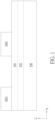
FIG. 1 ,FIG. 2 ,FIG. 3 ,FIG. 4 ,FIG. 5 andFIG. 6 are schematic cross-sectional diagrams illustrating a manufacturing method of an electronic device according to a first embodiment of the present disclosure, -
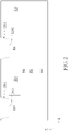
FIG. 7 is a partially enlarged schematic cross-sectional diagram of an electronic device according to the first embodiment of the present disclosure, -
FIG. 8 is a flow chart of steps of the manufacturing method of the electronic device according to the first embodiment of the present disclosure, -
FIG. 9 is a partially enlarged schematic cross-sectional diagram of an electronic device according to a second embodiment of the present disclosure, -
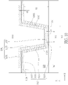
FIG. 10 is a partially enlarged schematic cross-sectional diagram of an electronic device according to a third embodiment of the present disclosure, -
FIG. 11 is a schematic top view of an opening of an insulating layer according to an embodiment of the present disclosure, and -
FIG. 12 is a schematic cross-sectional diagram of an electronic device according to a fourth embodiment of the present disclosure. - The contents of the present disclosure will be described in detail with reference to specific embodiments and drawings. It is noted that, for purposes of illustrative clarity and being easily understood by the readers, the following drawings may be simplified schematic diagrams of electronic devices or a portion of the electronic devices, and components therein may not be drawn to scale. The numbers and dimensions of the components in the drawings are just illustrative, and are not intended to limit the scope of the present disclosure.
- Certain terms are used throughout the specification and the appended claims of the present disclosure to refer to specific components. Those skilled in the art should understand that electronic equipment manufacturers may refer to a component by different names, and this document does not intend to distinguish between components that differ in name but not function. In the following description and claims, the terms "comprise", "include" and "have" are used in an open-ended fashion, so they should be interpreted as "including but not limited to...".
- It should be understood that when a component or layer is referred to as being "on" or "disposed on" another component or layer, or "connected to" another component or layer, it may be directly on the another component or layer or directly connected to the another component or layer, or there may be an interposed component or layer between the two components or layers (indirect case). Conversely, when a component is referred to as being "directly on" another component or layer, "directly disposed on" another component or layer, or "directly connected to" another component or layer, there are no interposed components or layers between the two components or layers. In addition, the arrangement relationship between different components may be explained by the content of the drawings.
- An electrical connection may be a direct connection or an indirect connection. When two elements are electrically connected, the electrical signals may be transmitted by direct contact, and there are no other elements presented between the two elements. When two elements are electrically connected, the electrical signals may be transmitted through the intermediate element bridging the two elements. The electrical connection may also be referred to as coupling.
- In addition, it should be understood that although the terms "first", "second", "third", etc. may be used herein to describe various components, these components should not be limited by these terms. These terms may be used to distinguish different components. The same terms may not be used in the claims, and the components in the claims may be described by the terms "first", "second", "third", etc. according to the order of the components presented in the claims. Thus, a first component discussed below may be termed as a second component in the claims without departing from the present disclosure.
- According to the embodiments of the present disclosure, the width, thickness, height or area of each component, or the distance or spacing between components may be measured by using an optical microscopy (OM), a scanning electron microscope (SEM), a film thickness profile measuring instrument (a-step), an ellipsometer, or other suitable methods. In detail, according to some embodiments, a scanning electron microscope may be used to obtain a cross-sectional structure image containing the components to be measured, and to measure the width, thickness, height or area of each component, or the distance or spacing between the components, and to obtain the volume of the component through appropriate methods (such as integration).
- Here, the terms "about", "equal to", "equal" or "the same", "substantially" or "approximately" usually mean within 20% of a given value, or within 10%, 5%, 3%, 2%, 1% or 0.5% of the given value.
- It should be understood that according to the following embodiments, features of different embodiments may be replaced, recombined or mixed to constitute other embodiments without departing from the spirit of the present disclosure.
- The electronic devices of the present disclosure may include, for example, a package component, a display device, an antenna device, a touch display device, a curved display device, or a non-rectangular display device (free shaped display device), but not limited thereto. The electronic devices may be bendable or flexible electronic devices. The electronic devices may include, for example, a light-emitting diode (LED), liquid crystal, fluorescence, phosphor, other suitable display medium, or a combination thereof, but not limited thereto. The light-emitting diode may include, for example, an organic light-emitting diode (OLED), an inorganic light-emitting diode (LED), a mini light emitting diode (mini-LED), a micro light emitting diode (micro-LED) or quantum dots (QDs) light emitting diode (such as QLED, QDLED), other suitable materials, or any combination thereof, but not limited thereto. The display devices may include, for example, a tiled display device, but not limited thereto.
- The antenna device may include, for example, a liquid crystal antenna, or other kinds of antenna, but not limited thereto. The antenna device may include, for example, a tiled antenna device, but not limited thereto. It should be noted that the electronic devices of the present disclosure may be any combination of the aforementioned devices, but not limited thereto. In addition, the appearance of the electronic devices may be rectangular, circular, polygonal, a shape with curved edges, or other suitable shapes. The electronic devices may have peripheral systems such as a driving system, a control system, a light source system, a shelf system, etc., to support a display device, an antenna device or a tiled device. The following electronic devices take a package component as an example, but not limited thereto.
- A direction X and a direction Z are shown in the following drawings. An
electronic device 10 of the present disclosure may for example be a package component, where theelectronic device 10 may include a plurality of insulating layers and a plurality of metal layers, and these insulating layers and these metal layers may for example form a redistribution layer (RDL) in the package component, but not limited thereto. In a schematic cross-sectional view (for example,FIG. 6 of the present disclosure), theelectronic device 10 may be formed of insulating layers and conductive layers stacked alternately one by one along the direction Z. - The direction Z may be the stacking direction of the insulating layers and the metal layers in the
electronic device 10, but not limited thereto. The direction X may be, for example, the extending direction of the insulating layer, but not limited thereto. The direction Z may be perpendicular to the direction X. The direction Z may also be referred to as a vertical projection direction or a top-view direction. The spatial relationship of the structure may be described according to the direction X and the direction Z in the following drawings. - Please refer to
FIG. 1 to FIG. 8 ,FIG. 1 to FIG. 6 are schematic cross-sectional diagrams illustrating a manufacturing method of an electronic device according to a first embodiment of the present disclosure, andFIG. 8 is a flow chart of steps of the manufacturing method of the electronic device according to the first embodiment of the present disclosure. As shown inFIG. 1 andFIG. 8 , a step S101 may be performed to form a first metal layer (such as a metal layer 1061) on asubstrate 100. Firstly, thesubstrate 100 may be provided, and the material of thesubstrate 100 may include glass, quartz, sapphire, polymers (such as polyimide (PI), polyethylene terephthalate (PET)) and/or other suitable materials to be used as a flexible substrate or a rigid substrate, but not limited thereto. - Next, a
release layer 102 may be formed on thesubstrate 100, and aseed layer 104 may be formed on therelease layer 102. For example, therelease layer 102 may be fully formed on thesubstrate 100, and theseed layer 104 may be fully formed on therelease layer 102, but not limited thereto. In some embodiments, the material of therelease layer 102 may include silicon oxide (SiOx), silicon nitride (SiNx), silicon oxynitride (SiOxNy), polymers (such as resin, epoxy resin, acrylic acid, polyimide, polyethylene terephthalate (PET)) or other suitable materials, but not limited thereto. In some embodiments, the material of the seed layer 104 (or the seed layers mentioned below) may include copper, titanium, aluminum, nickel, molybdenum, a combination thereof, or other suitable metal materials, but not limited thereto. For example, the seed layer 104 (or the seed layers mentioned below) may be formed by electroplating or other suitable processes, but not limited thereto. - Next, a metal layer 1061 (or may be referred to as a first metal layer) may be formed on the
seed layer 104. As shown inFIG. 1 , ametal layer 1063 may also be formed together with themetal layer 1061, but not limited thereto. In some embodiments, themetal layer 1063 and themetal layer 1061 may be formed separately, but not limited thereto. Themetal layer 1061 and themetal layer 1063 may be a patterned metal layer. In some embodiments, a metal layer may be formed over the entire surface of theseed layer 104, and the metal layer (or the metal layers mentioned below) may be formed by electroplating, physical vapor deposition (PVD), atomic layer deposition (ALD), metal organic chemical vapor deposition (MOCVD) or other suitable processes, but not limited thereto. Then, themetal layer 1061 and themetal layer 1063 may be formed by photolithography and etching processes, or themetal layer 1061 and themetal layer 1063 may be formed by removing unnecessary metal portions through laser, but not limited thereto. In some embodiments, themetal layer 1061 and themetal layer 1063 may be formed by a screen printing process, but not limited thereto. In some embodiments, the material of themetal layer 1061 and the metal layer 1063 (or the metal layers mentioned below) may include copper (Cu), titanium (Ti), aluminum (Al), nickel (Ni), molybdenum (Mo), a combination thereof, an alloy thereof, a combination of alloys of the aforementioned metals, or other suitable metal materials, but not limited thereto. - As shown in
FIG. 2 andFIG. 8 , then a step S103 may be performed to form an insulating layer 110 (or may be referred to as a first insulating layer) on thesubstrate 100 and the first metal layer (such as the metal layer 1061), where the insulatinglayer 110 includes a first opening (such as an opening OP11), and the first opening exposes an upper surface (such as an upper surface 1081) of the first metal layer. The material of the insulating layer 110 (or the insulating layers mentioned below) may include organic or inorganic insulating materials, but not limited thereto. In some embodiments, the material of the insulating layer 110 (or the insulating layers mentioned below) may include an organic insulating material, such as polyimide, but not limited thereto. In some embodiments, the material of the insulating layer 110 (or the insulating layers mentioned below) may include an inorganic insulating material, such as silicon oxide (SiOx), silicon nitride (SiNx) or silicon oxynitride (SiOxNy), but not limited thereto. - In some embodiments, an unpatterned insulating layer may be fully formed on the
seed layer 104, themetal layer 1061 and themetal layer 1063, and the unpatterned insulating layer may be formed by a suitable coating process, laminating process, physical vapor deposition (PVD), atomic layer deposition (ALD) or other suitable thin film deposition processes, but not limited thereto. Next, an opening OP11 and an opening OP13 may be formed by photolithography and etching processes, but not limited thereto. The opening OP11 may expose a portion of theupper surface 1081 of themetal layer 1061, and the opening OP13 may expose a portion of anupper surface 1083 of themetal layer 1063. - As shown in
FIG. 3 andFIG. 8 , then a step S105 may be performed to form an insulating layer (such as an insulatinglayer 1121, or may be referred to as a second insulating layer) on the insulatinglayer 110, where the insulating layer extends into the first opening (such as the opening OP11), the insulating layer includes a second opening (such as an opening OP21), and the second opening is disposed in the first opening. As shown inFIG. 3 , an insulatinglayer 1123 may also be formed together with the insulatinglayer 1121, but not limited thereto. The insulatinglayer 1121 and the insulatinglayer 1123 may be a patterned insulating layer. - In some embodiments, an unpatterned insulating layer may be fully formed on the insulating
layer 110, and the unpatterned insulating layer may be formed by slit coating, spin coating, thermal vapor deposition or other suitable thin film growth processes, but not limited thereto. The insulatinglayer 1121 and the insulatinglayer 1123 may be insulating layers of a single-layered material or a composite material. The insulatinglayer 1121 and the insulatinglayer 1123 may be formed together on the insulatinglayer 110, i.e., the unpatterned insulating layer fully formed on the insulatinglayer 110 is patterned by such as photolithography and etching processes to form the insulatinglayer 1121 and the insulatinglayer 1123, or the insulatinglayer 1121 and the insulatinglayer 1123 may be formed by removing unnecessary portions through laser, but not limited thereto. In some embodiments, the insulatinglayer 1121 and the insulatinglayer 1123 may be formed by a screen printing process, but not limited thereto. In some embodiments, the insulatinglayer 1121 and the insulatinglayer 1123 may be formed separately, but not limited thereto. In addition, the insulatinglayer 1121 and the insulatinglayer 1123 may be separated from each other without being in contact. - The insulating
layer 1121 may extend into the opening OP11, and the insulatinglayer 1121 may include the opening OP21. The insulatinglayer 1123 may extend into the opening OP13, and the insulatinglayer 1123 may include an opening OP23. The opening OP21 is disposed in the opening OP11, and the opening OP23 is disposed in the opening OP13. The opening OP21 may expose a portion of theupper surface 1081 of themetal layer 1061, and the opening OP23 may expose a portion of theupper surface 1083 of themetal layer 1063. - The opening OP21 of the insulating
layer 1121 has a width W1, the opening OP11 of the insulatinglayer 110 has a width W2, and the width W1 may be different from the width W2. As shown inFIG. 3 , the width W1 may be smaller than the width W2. In some embodiments, the ratio (W1/W2) of the width W1 of the opening OP21 of the insulatinglayer 1121 to the width W2 of the opening OP11 of the insulatinglayer 110 may be greater than or equal to 0.5 and less than 1. The opening OP23 and the opening OP13 may also have the same width ratio. For example, the width of the opening may be obtained by measuring the width of the bottom of the opening, and the bottom of the opening may expose the upper surface of the underlying layer. - In addition, please refer to
FIG. 11 , which is a schematic top view of the opening of the insulating layer. As shown inFIG. 11 , the area of the opening OP21 of the insulatinglayer 1121 may be different from the area of the opening OP11 of the insulatinglayer 110. For example, the area of the opening OP21 of the insulatinglayer 1121 may be smaller than the area of the opening OP11 of the insulatinglayer 110. In some embodiments, the ratio of the area of the opening OP21 of the insulatinglayer 1121 to the area of the opening OP11 of the insulatinglayer 110 may be greater than or equal to 0.05 and less than 1. The opening OP23 and the opening OP13 may also have the same area ratio. For example, the area of the opening may be obtained by measuring the area of the bottom of the opening. Furthermore, the shape of the opening as shown inFIG. 11 is merely an example, and the opening may have any suitable shape. - The materials of the insulating
layer 1121 and the insulating layer 1123 (or the insulating layers mentioned below) may include materials capable of forming a silicon bond with the material of an adjacent layer, but not limited thereto. For example, the materials of the insulatinglayer 1121 and the insulating layer 1123 (or the insulating layers mentioned below) may include a silane coupling agent, epoxy resin or other suitable organic materials, but not limited thereto. In some embodiments, a thickness T1 of the insulatinglayer 1121 and the insulatinglayer 1123 and a thickness T2 of the insulatinglayer 110 are different. As shown inFIG. 3 , the thickness T1 of the insulatinglayer 1121 and the insulatinglayer 1123 may be smaller than the thickness T2 of the insulatinglayer 110, but not limited thereto. For example, the thickness T2 of the insulatinglayer 110 may be measured along the direction Z, and the thickness T1 of a portion of the insulating layer 1121 (or the insulating layer 1123) located on the insulatinglayer 110 may be measured along the direction Z. - As shown in
FIG. 4 andFIG. 8 , then a step S107 may be performed to form a seed layer (such as a seed layer 1141) on the insulating layer (such as the insulating layer 1121), where the seed layer extends into the second opening (such as the opening OP21). As shown inFIG. 4 , aseed layer 1143 may also be formed together with theseed layer 1141, i.e., theseed layer 1141 and theseed layer 1143 may be a patterned seed layer, but not limited thereto. In some embodiments, theseed layer 1143 and theseed layer 1141 may be formed separately, but not limited thereto. - In some embodiments, an unpatterned seed layer may be fully formed on the insulating
layer 110, the insulatinglayer 1121 and the insulatinglayer 1123 by sputtering, thin film deposition or other suitable processes. Then, theseed layer 1141 and theseed layer 1143 may be formed by photolithography and etching processes, or theseed layer 1141 and theseed layer 1143 may be formed by removing unnecessary portions through laser, but not limited thereto. In some embodiments, theseed layer 1141 and theseed layer 1143 may be formed by a screen printing process, but not limited thereto. - The
seed layer 1141 may be formed on the insulatinglayer 1121 and extend into the opening OP21, and theseed layer 1141 may be in contact with a portion of theupper surface 1081 of themetal layer 1061 exposed by the opening OP21. Theseed layer 1143 may be formed on the insulatinglayer 1123 and extend into the opening OP23, and theseed layer 1143 may be in contact with a portion of theupper surface 1083 of themetal layer 1063 exposed by the opening OP23. Although theseed layer 1141 and theseed layer 1143 may be separated from each other inFIG. 4 , theseed layer 1141 and theseed layer 1143 may be electrically connected with each other or electrically isolated from each other. In addition, the insulatinglayer 1121 may be completely covered by theseed layer 1141, and the insulatinglayer 1123 may be completely covered by theseed layer 1143, but not limited thereto. - As shown in
FIG. 5 andFIG. 8 , then a step S109 may be performed to form a second metal layer (such as a metal layer 1161) on the seed layer (such as the seed layer 1141), where the second metal layer is electrically connected to the first metal layer (such as the metal layer 1061) through the first opening (such as the opening OP11) of the insulatinglayer 110 and the second opening (such as the opening OP21) of the insulating layer (such as the insulating layer 1121). Themetal layer 1161 and ametal layer 1163 may be a patterned metal layer. For example, themetal layer 1161 may be formed on theseed layer 1141 and themetal layer 1163 may be formed on theseed layer 1143 by electroplating or other suitable processes, but not limited thereto. - The
metal layer 1161 may be electrically connected to themetal layer 1061 through the opening OP11 of the insulatinglayer 110, the opening OP21 of the insulatinglayer 1121, and theseed layer 1141 in the opening OP21. Themetal layer 1163 may be electrically connected to themetal layer 1063 through the opening OP13 of the insulatinglayer 110, the opening OP23 of the insulatinglayer 1123, and theseed layer 1143 in the opening OP23. For example, themetal layer 1061, the insulatinglayer 110, the insulatinglayer 1121, theseed layer 1141 and themetal layer 1161 may constitute a portion of a redistribution layer (such as theelectronic device 10 ofFIG. 6 ), but not limited thereto. Themetal layer 1061 and themetal layer 1161 may be connection elements in the redistribution layer, but not limited thereto. - The metal layer (such as an inorganic material) and the insulating layer (such as an organic material) have different material properties, so that the adhesion between the metal layer and the insulating layer may be poor, thereby reducing the reliability of the electronic device. In the current technology, the insulating layer may be processed by a surface treatment to obtain a good adhesion between the insulating layer and the metal layer. However, the surface treatment requires using plasma in a vacuum environment, and the vacuum equipment is complicated and expensive.
- In the present disclosure, the insulating
layer 1121 may be formed between the insulatinglayer 110 and theseed layer 1141, where the insulatinglayer 1121 includes a silane coupling agent that increases the adhesion between the seed layer 1141 (or the metal layer 1161) and the insulatinglayer 110, so that the plasma surface treatment and the vacuum equipment may not be required. In this way, the reliability of the electronic device can be improved, and the cost thereof can also be saved. - Next, the aforementioned steps may be repeated to form a
stacked structure 20 of multiple metal layers and multiple insulating layers on themetal layer 1161 and themetal layer 1163. As shown inFIG. 6 , a plurality ofmetal layers 1161 and a plurality ofmetal layers 1163 may be formed on thesubstrate 100, and multiple insulatinglayers multiple metal layers metal layers 1161 and themetal layers 1163, but not limited thereto. The insulatinglayer 118 may be disposed between themetal layer 124 and the metal layer 1161 (or the metal layer 1163), and themetal layer 124 may be electrically connected to themetal layer 1161. The insulatinglayer 120 may be disposed between themetal layer 126 and themetal layer 124, and themetal layer 126 may be electrically connected to themetal layer 124. The insulatinglayer 122 may be disposed between themetal layer 128 and themetal layer 126, and themetal layer 128 may be electrically connected to themetal layer 126. The material of the insulatinglayers layer 110, but not limited thereto. - In addition, an insulating
layer 130 and aseed layer 132 may be formed between themetal layer 124 and the insulatinglayer 118, an insulatinglayer 134 and aseed layer 136 may be formed between themetal layer 126 and the insulatinglayer 120, and an insulatinglayer 138 and aseed layer 140 may be formed between themetal layer 128 and the insulatinglayer 122. The material of the insulatinglayers layer 1121, but not limited thereto. - Next, the
substrate 100 may be removed by removing therelease layer 102 inFIG. 1 , and a patterning process may be performed on theseed layer 104 inFIG. 1 to form one ormore metal layers 1421 and one ormore metal layers 1423. The pattern of themetal layer 1421 may be substantially the same as the pattern of themetal layer 1061, and the pattern of themetal layer 1423 may be substantially the same as the pattern of themetal layer 1063, but not limited thereto. - In addition, the
electronic device 10 of some embodiments may be a redistribution layer first (RDL first) package structure. As shown inFIG. 6 , achip 117 may be bonded to the aforementionedstacked structure 20 of metal layers and insulating layers. For example, contacts on thechip 117 may be bonded to themetal layer 128 throughbonding pads 119, but not limited thereto. - Please refer to
FIG. 7 , which is a partially enlarged schematic diagram of the electronic device according to the first embodiment of the present disclosure. As the aforementioned descriptions (seeFIG. 6 andFIG. 7 ), the present disclosure provides theelectronic device 10, which includes themetal layer 1061, the insulatinglayer 110, themetal layer 1161 and the insulatinglayer 1121. The insulatinglayer 110 may be disposed on themetal layer 1061, themetal layer 1161 may be disposed on the insulatinglayer 110, and the insulatinglayer 1121 may be disposed between themetal layer 1161 and the insulatinglayer 110. Themetal layer 1161 may be electrically connected to themetal layer 1061 through the opening OP11 of the insulatinglayer 110 and the opening OP21 of the insulatinglayer 1121. - As shown in
FIG. 7 , the insulatinglayer 110 may include anupper surface 1101 and aside surface 1103, and theside surface 1103 may be connected with theupper surface 1101. Theupper surface 1101 may extend substantially along the direction X, the extension direction of theside surface 1103 is different from the extension direction of theupper surface 1101, and theside surface 1103 may be an inclined surface. - The insulating
layer 1121 may include aportion 1131 and aportion 1133, and theportion 1133 may be connected with theportion 1131. Theportion 1131 of the insulatinglayer 1121 may be disposed on theupper surface 1101 of the insulatinglayer 110, and theportion 1131 of the insulatinglayer 1121 can extend substantially along the direction X, i.e., the extending direction of theportion 1131 of the insulatinglayer 1121 may be the same as the extending direction of theupper surface 1101 of the insulatinglayer 110. The extending direction of theportion 1133 of the insulatinglayer 1121 may be different from the extending direction of theportion 1131 of the insulatinglayer 1121, the extending direction of theportion 1133 of the insulatinglayer 1121 may be the same as the extending direction of theside surface 1103 of the insulatinglayer 110, and theportion 1133 of the insulatinglayer 1121 may be disposed on theside surface 1103 of the insulatinglayer 110. - The
seed layer 1141 may include aportion 1151, aportion 1153, and aportion 1155, and theportion 1153 may be connected with theportion 1151 and theportion 1155. One end of theportion 1153 may be connected to theportion 1151, and another end of theportion 1153 may be connected to theportion 1155. Theportion 1151 of theseed layer 1141 may be disposed on theportion 1131 of the insulatinglayer 1121 and may completely cover theportion 1131 of the insulatinglayer 1121, but not limited thereto. Theportion 1153 of theseed layer 1141 may be disposed on theportion 1133 of the insulatinglayer 1121 and may completely cover theportion 1133 of the insulatinglayer 1121, but not limited thereto. Theportion 1155 of theseed layer 1141 may be disposed on a portion of theupper surface 1081 of themetal layer 1061 within the opening OP21. Theportion 1151 and theportion 1155 may extend substantially along the direction X, i.e., the extending direction of theportion 1151 and theportion 1155 may be the same as the extending direction of theupper surface 1101 of the insulatinglayer 110. The extending direction of theportion 1153 may be different from the extending direction of theportion 1151 or theportion 1155, and the extending direction of theportion 1153 may be the same as the extending direction of theside surface 1103 of the insulatinglayer 110. - In addition, the electronic device 10 (as shown in
FIG. 6 andFIG. 7 ) may include a package structure, and may include a redistribution layer (such as the stack structure 20) in the package structure, but not limited thereto. The redistribution layer (such as theelectronic device 10 or the stackedstructure 20 therein) may include at least themetal layer 1061, the insulatinglayer 110, the insulatinglayer 1121 and themetal layer 1161. In addition, the metal layers in theelectronic device 10 may be, for example, connection elements in the redistribution layer, but not limited thereto. - The electronic devices and the manufacturing methods thereof of the present disclosure are not limited to the aforementioned embodiments. The following will continue to disclose other embodiments of the present disclosure. However, in order to simplify the description and highlight the differences between the embodiments, the same reference numerals are used to denote the same elements hereinafter, and the repeated portions will not be described again.
- Please refer to
FIG. 9 , which is a partially enlarged schematic cross-sectional diagram of an electronic device according to a second embodiment of the present disclosure. The difference between this embodiment and the first embodiment (as shown inFIG. 7 ) is that the insulatinglayer 1121 may further include aportion 1135, and theportion 1133 may be connected with theportion 1131 and theportion 1135. One end of theportion 1133 may be connected to theportion 1131, and another end of theportion 1133 may be connected to theportion 1135. Theportion 1131 and theportion 1135 may extend substantially along the direction X, i.e., the extending direction of theportion 1131 and theportion 1135 may be the same as the extending direction of theupper surface 1101 of the insulatinglayer 110. The extending direction of theportion 1133 may be different from the extending direction of theportion 1131 or theportion 1135, and the extending direction of theportion 1133 may be the same as the extending direction of theside surface 1103 of the insulatinglayer 110. - The
portion 1135 of the insulatinglayer 1121 may be disposed on a portion of theupper surface 1081 of themetal layer 1061 within the opening OP11, and theportion 1135 may extend in the direction X. Furthermore, theportion 1135 may be covered by theportion 1153 and/or theportion 1155 of theseed layer 1141, and at least a portion of the insulating layer 1121 (such as the portion 1135) may be overlapped with themetal layer 1061 within the opening OP11. - Since the insulating
layer 1121 may further include theportion 1135, the width of the opening OP21 may be further reduced. The opening OP21 of this embodiment (as shown inFIG. 9 ) has a width W3, and the width W3 is smaller than the width W1 of the opening OP21 of the first embodiment (as shown inFIG. 7 ). In addition, the area of the opening OP21 of this embodiment may also be smaller than the area of the opening OP21 of the first embodiment. For example, when the shape of the opening is circular, the ratio (W3/W2) of the width W3 of the opening OP21 of the insulatinglayer 1121 to the width W2 of the opening OP11 of the insulatinglayer 110 may be greater than or equal to 0.5 and less than 1. The ratio of the area of the opening OP21 to the area of the opening OP11 may be greater than or equal to 0.05 and less than 1. The shape of the opening may optionally be other suitable shapes, but not limited thereto. - Please refer to
FIG. 10 , which is a partially enlarged schematic cross-sectional diagram of an electronic device according to a third embodiment of the present disclosure. The difference between this embodiment and the second embodiment (as shown inFIG. 9 ) is that the insulatinglayer 1121 may further include aportion 1137, and theportion 1131 may be connected with theportion 1137 and theportion 1133. One end of theportion 1131 may be connected to theportion 1137, and another end of theportion 1131 may be connected to theportion 1133. Theportion 1137 and theportion 1131 may be disposed on theupper surface 1101 of the insulatinglayer 110. In addition, theportion 1151 of theseed layer 1141 may be disposed on theportion 1131 of the insulatinglayer 1121, and theportion 1151 of theseed layer 1141 may cover theportion 1131 of the insulatinglayer 1121 but not cover theportion 1137 of the insulatinglayer 1121. - Please refer to
FIG. 12 , which is a cross-sectional schematic diagram of an electronic device according to a fourth embodiment of the present disclosure. In some embodiments (as shown inFIG. 12 ), theelectronic device 10 may be a chip first package structure. As shown inFIG. 12 , the stackedstructure 20 of the metal layers and the insulating layers may be disposed on amolding layer 121 and achip 117, or themolding layer 121 and thechip 117 may be formed on the stackedstructure 20 of the metal layers and the insulating layers, but not limited thereto. Thechip 117 may be disposed in themolding layer 121, and the stackedstructure 20 may be bonded to contacts on thechip 117 through themetal layer 1421 and themetal layer 1423, but not limited thereto. In some embodiments of the chip first package structure (as shown inFIG. 12 ) and the manufacturing method thereof, thesubstrate 100 and therelease layer 102 inFIG. 1 may not be included, but not limited thereto. - In addition, in some embodiments of the chip first package structure and the manufacturing method thereof, the
substrate 100 and therelease layer 102 inFIG. 1 may be included, but not limited thereto. For example, thesubstrate 100 and therelease layer 102 may be disposed under themolding layer 121 and thechip 117, or therelease layer 102 may be disposed between thechip 117 and thesubstrate 100, and between themolding layer 121 and thesubstrate 100, but not limited thereto. - In summary, in the electronic devices and the manufacturing methods thereof of the present disclosure, a second insulating layer may be formed between a first insulating layer and a seed layer, where the second insulating layer includes a silane coupling agent that enhances the adhesion between the seed layer (or the metal layer) and the first insulating layer, and a plasma surface treatment and a vacuum equipment may not be required. In this way, the reliability of the electronic devices can be improved, and the cost thereof can also be saved.
Claims (10)
- An electronic device (10), characterized by comprising:a first metal layer (1061, 1063);a first insulating layer (110) disposed on the first metal layer (1061, 1063);a second metal layer (1161, 1163) disposed on the first insulating layer (110); anda second insulating layer (1121, 1123) disposed between the second metal layer (1161, 1163) and the first insulating layer (110),wherein the second metal layer (1161, 1163) is electrically connected to the first metal layer (1061, 1063) through a first opening (OP11, OP13) of the first insulating layer (110) and a second opening (OP21, OP23) of the second insulating layer (1121, 1123).
- The electronic device (10) according to claim 1, characterized in that a thickness (T1) of the second insulating layer (1121, 1123) is different from a thickness (T2) of the first insulating layer (110).
- The electronic device (10) according to any one of claims 1 to 2, characterized in that a ratio of a width (W1) of the second opening (OP21, OP23) of the second insulating layer (1121, 1123) to a width (W2) of the first opening (OP11, OP13) of the first insulating layer (110) is greater than or equal to 0.5 and less than 1.
- The electronic device (10) according to any one of claims 1 to 3, characterized in that at least a portion (1135) of the second insulating layer (1121) is overlapped with the first metal layer (1061) within the first opening (OP11).
- The electronic device (10) according to any one of claims 1 to 4, further characterized by comprising a redistribution layer, wherein the redistribution layer comprises the first metal layer (1061, 1063), the first insulating layer (110), the second insulating layer (1121, 1123) and the second metal layer (1161, 1163).
- A manufacturing method of an electronic device (10), characterized by comprising:forming a first metal layer (1061, 1063) on a substrate (100);forming a first insulating layer (110) on the substrate (100) and the first metal layer (1061, 1063), wherein the first insulating layer (110) comprises a first opening (OP11, OP13), and the first opening (OP11, OP13) exposes an upper surface (1081, 1083) of the first metal layer (1061, 1063);forming a second insulating layer (1121, 1123) on the first insulating layer (110), wherein the second insulating layer (1121, 1123) extends into the first opening (OP11, OP13), the second insulating layer (1121, 1123) comprises a second opening (OP21, OP23), and the second opening (OP21, OP23) is disposed in the first opening (OP11, OP13);forming a seed layer (1141, 1143) on the second insulating layer (1121, 1123), wherein the seed layer (1141, 1143) extends into the second opening (OP21, OP23); andforming a second metal layer (1161, 1163) on the seed layer (1141, 1143), wherein the second metal layer (1161, 1163) is electrically connected to the first metal layer (1061, 1063) through the first opening (OP11, OP13) of the first insulating layer (110) and the second opening (OP21, OP23) of the second insulating layer (1121, 1123).
- The manufacturing method of the electronic device (10) according to claim 6, characterized in that a thickness (T1) of the second insulating layer (1121, 1123) is different from a thickness (T2) of the first insulating layer (110).
- The manufacturing method of the electronic device (10) according to any one of claims 6 to 7, characterized in that a ratio of a width (W1) of the second opening (OP21, OP23) of the second insulating layer (1121, 1123) to a width (W2) of the first opening (OP11, OP13) of the first insulating layer (110) is greater than or equal to 0.5 and less than 1.
- The manufacturing method of the electronic device (10) according to any one of claims 6 to 8, characterized in that at least a portion (1135) of the second insulating layer (1121) is overlapped with the first metal layer (1061) within the first opening (OP11).
- The manufacturing method of the electronic device (10) according to any one of claims 6 to 9, characterized in that the first metal layer (1061, 1063), the first insulating layer (110), the second insulating layer (1121, 1123) and the second metal layer (1161, 1163) constitute a redistribution layer.
Applications Claiming Priority (1)
| Application Number | Priority Date | Filing Date | Title |
|---|---|---|---|
| CN202111094921.5A CN115831923A (en) | 2021-09-17 | 2021-09-17 | Electronic device and manufacturing method thereof |
Publications (1)
| Publication Number | Publication Date |
|---|---|
| EP4152364A1 true EP4152364A1 (en) | 2023-03-22 |
Family
ID=83004868
Family Applications (1)
| Application Number | Title | Priority Date | Filing Date |
|---|---|---|---|
| EP22191114.2A Withdrawn EP4152364A1 (en) | 2021-09-17 | 2022-08-19 | Electronic device and manufacturing method thereof |
Country Status (5)
| Country | Link |
|---|---|
| US (1) | US12368105B2 (en) |
| EP (1) | EP4152364A1 (en) |
| KR (1) | KR20230041598A (en) |
| CN (1) | CN115831923A (en) |
| TW (1) | TW202315019A (en) |
Citations (3)
| Publication number | Priority date | Publication date | Assignee | Title |
|---|---|---|---|---|
| EP1691414A2 (en) * | 2005-02-14 | 2006-08-16 | Fujitsu Limited | Semiconductor device, method of manufacturing the same, capacitor structure, and method of manufacturing the same |
| US20190051607A1 (en) * | 2017-08-10 | 2019-02-14 | Samsung Electronics Co., Ltd. | Semiconductor package and method of fabricating the same |
| US20200105689A1 (en) * | 2018-09-27 | 2020-04-02 | Taiwan Semiconductor Manufacturing Co., Ltd. | Semiconductor device and manufacturing method thereof |
Family Cites Families (6)
| Publication number | Priority date | Publication date | Assignee | Title |
|---|---|---|---|---|
| US7368377B2 (en) * | 2004-12-09 | 2008-05-06 | Interuniversitair Microelektronica Centrum (Imec) Vzw | Method for selective deposition of a thin self-assembled monolayer |
| KR100596452B1 (en) | 2005-03-22 | 2006-07-04 | 삼성전자주식회사 | Wafer Level Chipscale Package with Air Gap between Ball Land and Solder Ball and Manufacturing Method Thereof |
| US9318452B2 (en) | 2014-03-21 | 2016-04-19 | Taiwan Semiconductor Manufacturing Company, Ltd. | Semiconductor packages and methods of forming the same |
| CN107104058A (en) * | 2017-06-21 | 2017-08-29 | 中芯长电半导体(江阴)有限公司 | Fan-out-type list die package structure and preparation method thereof |
| US10923421B2 (en) * | 2019-04-23 | 2021-02-16 | Taiwan Semiconductor Manufacturing Company, Ltd. | Package structure and method of manufacturing the same |
| US11127628B1 (en) * | 2020-03-16 | 2021-09-21 | Nanya Technology Corporation | Semiconductor device with connecting structure having a step-shaped conductive feature and method for fabricating the same |
-
2021
- 2021-09-17 CN CN202111094921.5A patent/CN115831923A/en not_active Withdrawn
-
2022
- 2022-01-06 TW TW111100531A patent/TW202315019A/en unknown
- 2022-05-03 US US17/736,067 patent/US12368105B2/en active Active
- 2022-08-19 KR KR1020220104302A patent/KR20230041598A/en active Pending
- 2022-08-19 EP EP22191114.2A patent/EP4152364A1/en not_active Withdrawn
Patent Citations (3)
| Publication number | Priority date | Publication date | Assignee | Title |
|---|---|---|---|---|
| EP1691414A2 (en) * | 2005-02-14 | 2006-08-16 | Fujitsu Limited | Semiconductor device, method of manufacturing the same, capacitor structure, and method of manufacturing the same |
| US20190051607A1 (en) * | 2017-08-10 | 2019-02-14 | Samsung Electronics Co., Ltd. | Semiconductor package and method of fabricating the same |
| US20200105689A1 (en) * | 2018-09-27 | 2020-04-02 | Taiwan Semiconductor Manufacturing Co., Ltd. | Semiconductor device and manufacturing method thereof |
Also Published As
| Publication number | Publication date |
|---|---|
| US20230089751A1 (en) | 2023-03-23 |
| TW202315019A (en) | 2023-04-01 |
| US12368105B2 (en) | 2025-07-22 |
| CN115831923A (en) | 2023-03-21 |
| KR20230041598A (en) | 2023-03-24 |
Similar Documents
| Publication | Publication Date | Title |
|---|---|---|
| US10325892B2 (en) | Light emitting device and manufacturing method thereof | |
| US8728871B2 (en) | Method for fabricating electronic device package | |
| US20100181589A1 (en) | Chip package structure and method for fabricating the same | |
| US20100001305A1 (en) | Semiconductor devices and fabrication methods thereof | |
| US7847299B2 (en) | Semiconductor device and method of manufacturing the same | |
| TW202026732A (en) | Pixel structure and repairing method thereof | |
| US20250372406A1 (en) | Manufacturing method of package structure of electronic device | |
| US20230131636A1 (en) | Micro light-emitting diode package structure | |
| CN112997314B (en) | Display back plate, manufacturing method thereof and display device | |
| US12368105B2 (en) | Electronic device having a silane coupling agent in an insulating layer | |
| CN118284256B (en) | OLED display screen and preparation method thereof | |
| US20240243028A1 (en) | Electronic device and manufacturing method of the same | |
| US20230380071A1 (en) | Electronic device | |
| CN119403333A (en) | Display Devices | |
| US20230070973A1 (en) | Package structure, display device and manufacturing method thereof | |
| US20230411230A1 (en) | Electronic device and manufacturing method thereof | |
| TWI915046B (en) | Package structure | |
| TWI850679B (en) | Electronic device and manufacturing method thereof | |
| CN112909136A (en) | Light emitting diode, display panel, display device and preparation method | |
| US20260005151A1 (en) | Electronic device | |
| US20250046991A1 (en) | Electronic device and method of manufacturing the same | |
| US20240355985A1 (en) | Electronic device | |
| US12456670B2 (en) | Electronic device | |
| EP4131373A2 (en) | Package device | |
| US12374560B2 (en) | Method for manufacturing electronic device |
Legal Events
| Date | Code | Title | Description |
|---|---|---|---|
| PUAI | Public reference made under article 153(3) epc to a published international application that has entered the european phase |
Free format text: ORIGINAL CODE: 0009012 |
|
| STAA | Information on the status of an ep patent application or granted ep patent |
Free format text: STATUS: THE APPLICATION HAS BEEN PUBLISHED |
|
| AK | Designated contracting states |
Kind code of ref document: A1 Designated state(s): AL AT BE BG CH CY CZ DE DK EE ES FI FR GB GR HR HU IE IS IT LI LT LU LV MC MK MT NL NO PL PT RO RS SE SI SK SM TR |
|
| STAA | Information on the status of an ep patent application or granted ep patent |
Free format text: STATUS: REQUEST FOR EXAMINATION WAS MADE |
|
| 17P | Request for examination filed |
Effective date: 20230915 |
|
| RBV | Designated contracting states (corrected) |
Designated state(s): AL AT BE BG CH CY CZ DE DK EE ES FI FR GB GR HR HU IE IS IT LI LT LU LV MC MK MT NL NO PL PT RO RS SE SI SK SM TR |
|
| STAA | Information on the status of an ep patent application or granted ep patent |
Free format text: STATUS: THE APPLICATION HAS BEEN WITHDRAWN |
|
| 18W | Application withdrawn |
Effective date: 20260120 |