EP4151153B1 - Elektrokardiogrammüberwachungsvorrichtung und überwachungsschaltung - Google Patents
Elektrokardiogrammüberwachungsvorrichtung und überwachungsschaltung Download PDFInfo
- Publication number
- EP4151153B1 EP4151153B1 EP21821452.6A EP21821452A EP4151153B1 EP 4151153 B1 EP4151153 B1 EP 4151153B1 EP 21821452 A EP21821452 A EP 21821452A EP 4151153 B1 EP4151153 B1 EP 4151153B1
- Authority
- EP
- European Patent Office
- Prior art keywords
- circuit
- electrode
- potential
- voltage
- housing
- Prior art date
- Legal status (The legal status is an assumption and is not a legal conclusion. Google has not performed a legal analysis and makes no representation as to the accuracy of the status listed.)
- Active
Links
Images







Classifications
-
- A—HUMAN NECESSITIES
- A61—MEDICAL OR VETERINARY SCIENCE; HYGIENE
- A61B—DIAGNOSIS; SURGERY; IDENTIFICATION
- A61B5/00—Measuring for diagnostic purposes; Identification of persons
- A61B5/24—Detecting, measuring or recording bioelectric or biomagnetic signals of the body or parts thereof
- A61B5/25—Bioelectric electrodes therefor
- A61B5/251—Means for maintaining electrode contact with the body
- A61B5/256—Wearable electrodes, e.g. having straps or bands
-
- A—HUMAN NECESSITIES
- A61—MEDICAL OR VETERINARY SCIENCE; HYGIENE
- A61B—DIAGNOSIS; SURGERY; IDENTIFICATION
- A61B5/00—Measuring for diagnostic purposes; Identification of persons
- A61B5/24—Detecting, measuring or recording bioelectric or biomagnetic signals of the body or parts thereof
- A61B5/25—Bioelectric electrodes therefor
- A61B5/279—Bioelectric electrodes therefor specially adapted for particular uses
- A61B5/28—Bioelectric electrodes therefor specially adapted for particular uses for electrocardiography [ECG]
-
- A—HUMAN NECESSITIES
- A61—MEDICAL OR VETERINARY SCIENCE; HYGIENE
- A61B—DIAGNOSIS; SURGERY; IDENTIFICATION
- A61B5/00—Measuring for diagnostic purposes; Identification of persons
- A61B5/24—Detecting, measuring or recording bioelectric or biomagnetic signals of the body or parts thereof
- A61B5/25—Bioelectric electrodes therefor
- A61B5/279—Bioelectric electrodes therefor specially adapted for particular uses
- A61B5/28—Bioelectric electrodes therefor specially adapted for particular uses for electrocardiography [ECG]
- A61B5/282—Holders for multiple electrodes
-
- A—HUMAN NECESSITIES
- A61—MEDICAL OR VETERINARY SCIENCE; HYGIENE
- A61B—DIAGNOSIS; SURGERY; IDENTIFICATION
- A61B5/00—Measuring for diagnostic purposes; Identification of persons
- A61B5/24—Detecting, measuring or recording bioelectric or biomagnetic signals of the body or parts thereof
- A61B5/30—Input circuits therefor
-
- A—HUMAN NECESSITIES
- A61—MEDICAL OR VETERINARY SCIENCE; HYGIENE
- A61B—DIAGNOSIS; SURGERY; IDENTIFICATION
- A61B5/00—Measuring for diagnostic purposes; Identification of persons
- A61B5/24—Detecting, measuring or recording bioelectric or biomagnetic signals of the body or parts thereof
- A61B5/30—Input circuits therefor
- A61B5/305—Common mode rejection
-
- A—HUMAN NECESSITIES
- A61—MEDICAL OR VETERINARY SCIENCE; HYGIENE
- A61B—DIAGNOSIS; SURGERY; IDENTIFICATION
- A61B5/00—Measuring for diagnostic purposes; Identification of persons
- A61B5/24—Detecting, measuring or recording bioelectric or biomagnetic signals of the body or parts thereof
- A61B5/30—Input circuits therefor
- A61B5/307—Input circuits therefor specially adapted for particular uses
- A61B5/308—Input circuits therefor specially adapted for particular uses for electrocardiography [ECG]
-
- A—HUMAN NECESSITIES
- A61—MEDICAL OR VETERINARY SCIENCE; HYGIENE
- A61B—DIAGNOSIS; SURGERY; IDENTIFICATION
- A61B5/00—Measuring for diagnostic purposes; Identification of persons
- A61B5/24—Detecting, measuring or recording bioelectric or biomagnetic signals of the body or parts thereof
- A61B5/316—Modalities, i.e. specific diagnostic methods
- A61B5/318—Heart-related electrical modalities, e.g. electrocardiography [ECG]
-
- A—HUMAN NECESSITIES
- A61—MEDICAL OR VETERINARY SCIENCE; HYGIENE
- A61B—DIAGNOSIS; SURGERY; IDENTIFICATION
- A61B5/00—Measuring for diagnostic purposes; Identification of persons
- A61B5/68—Arrangements of detecting, measuring or recording means, e.g. sensors, in relation to patient
- A61B5/6801—Arrangements of detecting, measuring or recording means, e.g. sensors, in relation to patient specially adapted to be attached to or worn on the body surface
- A61B5/6802—Sensor mounted on worn items
- A61B5/681—Wristwatch-type devices
-
- A—HUMAN NECESSITIES
- A61—MEDICAL OR VETERINARY SCIENCE; HYGIENE
- A61B—DIAGNOSIS; SURGERY; IDENTIFICATION
- A61B5/00—Measuring for diagnostic purposes; Identification of persons
- A61B5/68—Arrangements of detecting, measuring or recording means, e.g. sensors, in relation to patient
- A61B5/6801—Arrangements of detecting, measuring or recording means, e.g. sensors, in relation to patient specially adapted to be attached to or worn on the body surface
- A61B5/683—Means for maintaining contact with the body
- A61B5/6831—Straps, bands or harnesses
-
- A—HUMAN NECESSITIES
- A61—MEDICAL OR VETERINARY SCIENCE; HYGIENE
- A61B—DIAGNOSIS; SURGERY; IDENTIFICATION
- A61B2560/00—Constructional details of operational features of apparatus; Accessories for medical measuring apparatus
- A61B2560/02—Operational features
- A61B2560/0204—Operational features of power management
- A61B2560/0214—Operational features of power management of power generation or supply
-
- A—HUMAN NECESSITIES
- A61—MEDICAL OR VETERINARY SCIENCE; HYGIENE
- A61B—DIAGNOSIS; SURGERY; IDENTIFICATION
- A61B2560/00—Constructional details of operational features of apparatus; Accessories for medical measuring apparatus
- A61B2560/04—Constructional details of apparatus
-
- A—HUMAN NECESSITIES
- A61—MEDICAL OR VETERINARY SCIENCE; HYGIENE
- A61B—DIAGNOSIS; SURGERY; IDENTIFICATION
- A61B2562/00—Details of sensors; Constructional details of sensor housings or probes; Accessories for sensors
- A61B2562/18—Shielding or protection of sensors from environmental influences, e.g. protection from mechanical damage
- A61B2562/182—Electrical shielding, e.g. using a Faraday cage
Definitions
- This disclosure relates to the field of electronic technologies, and the invention in particular relates to an electrocardiogram detection device.
- the wearable devices such as a smartwatch (or a smart band) usually have an electrocardiogram (electrocardiogram, ECG) detection function.
- ECG electrocardiogram
- an ECG detection circuit may be integrated into the smartwatch, and the ECG detection circuit may be separately connected to a left arm (left arm, LA) electrode, a right arm (right arm, RA) electrode, and a right leg (right leg, RL) electrode.
- the ECG detection circuit may collect an ECG signal of a user by using the LA electrode and the RA electrode, and may provide a reference potential for the user by using the RL electrode, to ensure detection reliability.
- the LA electrode and the RL electrode are usually disposed on an outer side of a bottom cover of the smartwatch, that is, a side on which the bottom cover is in contact with skin of the user.
- the RA electrode is usually disposed on a watch housing of the smartwatch.
- the LA electrode and the RL electrode may be in contact with the skin of the user. If the user needs to perform ECG detection, the user may touch the RA electrode by using the right hand. In this case, the ECG circuit may collect the ECG signal of the user and perform ECG detection.
- the metal watch housing When the watch housing of the smartwatch is made of metal, to ensure anti-electromagnetic interference and antistatic performance of the smartwatch, the metal watch housing is grounded. Therefore, if the right hand of the user accidentally touches the metal watch housing when touching the RA electrode to perform ECG detection, the RL electrode forms a current path with the metal watch housing through the human body. Because there is a potential difference between the RL electrode and the metal watch housing, a path of a leakage current is formed between the RL electrode and the metal watch housing, and the leakage current affects accuracy of ECG detection.
- US 2020/064774 A1 discloses an electronic device, such as a watch, has a crown assembly having a shaft and a user-rotatable crown.
- the user-rotatable crown may include a conductive cap that is mechanically and electrically coupled to the shaft and functions as an electrode.
- the conductive cap may be coupled to the shaft using solder or another conductive attachment mechanism.
- the shaft may electrically couple the conductive cap to a processing unit of the electronic device.
- One or more additional electrodes may be positioned on the exterior surface of the electronic device.
- the conductive cap is operable to be contacted by a finger of a user of the electronic device while another electrode is positioned against skin of the user.
- the processing unit of the electronic device is operable to determine a biological parameter, such as an electrocardiogram, of the user based on voltages at the electrodes.
- the object of the present invention is to provide an electrocardiogram detection device, to resolve a problem in the related technology that a leakage current generated in a metal housing affects accuracy of ECG detection.
- an electrocardiogram detection device may include a housing made of a conductive material, an electrocardiogram detection circuit and a voltage holder circuit that are disposed in the housing, and a first electrode, a second electrode, and a third electrode that are disposed outside the housing and insulated from the housing.
- the three electrodes are in contact with skin of a user.
- the electrocardiogram detection circuit may be separately connected to the first electrode, the second electrode, and the third electrode.
- the electrocardiogram detection circuit is configured to collect an electrocardiogram signal by using the first electrode and the second electrode, and provide a reference potential for the third electrode.
- the voltage holder circuit is connected to the housing, and is configured to provide a target potential for the housing.
- a potential difference between the target potential and the reference potential is less than a difference threshold.
- the potential difference between the target potential provided by the voltage holder circuit and the reference potential provided by the electrocardiogram detection circuit for the third electrode is small. Therefore, in an ECG detection process, even if the user accidentally touches the housing and causes the housing to be conducted to the third electrode, no leakage current is generated between the housing and the third electrode or a small leakage current is generated between the housing and the third electrode. This can effectively reduce interference to an ECG signal and ensure accuracy of ECG detection.
- an output end of the voltage holder circuit is connected to the housing, an input end of the voltage holder circuit is connected to a potential provider, and the voltage holder circuit is configured to output the target potential at the output end based on an input signal of the input end. Because the voltage holder circuit may output the target potential at the output end based on the signal input at the input end of the voltage holder circuit, and the potential difference between the target potential and the reference potential of the third electrode is small, the leakage current between the housing and the third electrode can be effectively suppressed, and accuracy of ECG detection can be ensured.
- the potential provider is the third electrode, or the second electrode, or the first electrode, or a power supply output end.
- the potential provider is the third electrode, this can ensure that the target potential provided by the voltage holder circuit for the housing is approximately equal to the reference potential of the third electrode. This can effectively suppress the leakage current.
- the potential provider is the second electrode or the first electrode, because a potential difference between potentials of the two electrodes and the reference potential of the third electrode is small, the leakage current between the third electrode and the housing can also be effectively reduced.
- the potential provider is the power supply output end, a potential of the power supply output end may be properly designed, so that the target potential provided by the voltage holder circuit for the housing is approximately equal to the reference potential. This can ensure suppression on the leakage current.
- the potential provider is the third electrode, or the second electrode, or the first electrode.
- the voltage holder circuit is a voltage follower circuit. An output end of the voltage follower circuit serves as the output end of the voltage holder circuit and is connected to the housing. An input end of the voltage follower circuit serves as the input end of the voltage holder circuit and is connected to the potential provider.
- the voltage follower circuit is configured to control a potential of the housing to be substantially consistent with the target potential of the potential provider. By using the voltage follower circuit, the potential of the housing may be substantially consistent with the target potential of the third electrode, the second electrode, or the first electrode. This can effectively suppress the leakage current.
- the voltage follower circuit may include a first operational amplifier.
- An in-phase input end of the first operational amplifier serves as the input end of the voltage follower circuit and is connected to the potential provider.
- An output end of the first operational amplifier serves as the output end of the voltage follower circuit and is separately connected to the housing and an out-of-phase input end of the first operational amplifier. Voltage following can be achieved by connecting the output end of the operational amplifier to the out-of-phase input end.
- an input resistance of the first operational amplifier is high (the input resistance is infinite in an ideal case), impact on the potential of the potential provider can be avoided, and it is ensured that the electrocardiogram detection circuit can run normally.
- the voltage follower circuit may further include a plurality of cascaded first operational amplifiers.
- the voltage follower circuit may include a plurality of cascaded discrete triodes. These circuits can also achieves effect similar to that of an operational amplifier, and it is ensured that the electrocardiogram detection circuit can run normally.
- the potential provider is the power supply output end.
- the voltage holder circuit is a voltage regulator circuit. An input end of the voltage regulator circuit serves as the input end of the voltage holder circuit and is connected to the power supply end. An output end of the voltage regulator circuit serves as the output end of the voltage holder circuit and is connected to the housing.
- the voltage regulator circuit is configured to provide the target potential for the housing under driving of the power supply end.
- the target potential provided by the voltage regulator circuit may be equal to a potential of a reference power supply end connected to a right leg drive sub-circuit. Therefore, this can ensure that the potential difference between the target potential and the reference potential provided by the right leg drive sub-circuit for the third electrode is small. This can effectively suppress the leakage current.
- the voltage regulator circuit may be a low dropout regulator (low dropout regulator, LDO).
- LDO low dropout regulator
- the LDO has advantages such as low noise and a small static current.
- the target potential is equal to or close to the reference potential, so that the leakage current between the housing and the third electrode can be effectively suppressed.
- the electrocardiogram detection device may further include a resistor connected in series between the housing and the voltage holder circuit.
- the resistor may further increase a resistance on a path of the leakage current. In this way, the leakage current can be effectively reduced.
- the electrocardiogram detection device may further include a capacitor connected in parallel to the resistor.
- the capacitor can ensure anti-electromagnetic interference and antistatic performance of the electrocardiogram detection device.
- the electrocardiogram detection device may further include an ESD circuit disposed in the housing. One end of the ESD circuit is connected to the housing, and the other end is grounded. The ESD circuit can prevent each electronic component in the electrocardiogram detection device from being damaged by electrostatic.
- the ESD circuit may include a transient voltage suppressor (transient voltage suppressor, TVS).
- a transient voltage suppressor transient voltage suppressor
- One electrode of the TVS is connected to the housing, and the other electrode of the TVS is grounded.
- the TVS has advantages of a fast response, a high transient power, a small leakage current, a small breakdown voltage deviation, easy control of clamping voltage, no damage limit, and a small size.
- the electrocardiogram detection circuit may include a detection sub-circuit and the right leg drive sub-circuit.
- a first input end of the detection sub-circuit is connected to the first electrode.
- a second input end of the detection sub-circuit is connected to the second electrode.
- a common-mode output end of the detection sub-circuit is connected to a first input end of the right leg drive sub-circuit.
- the detection sub-circuit is configured to collect an electrocardiogram signal, and output a common-mode voltage between the first input end and the second input end to the right leg drive sub-circuit.
- a second input end of the right leg drive sub-circuit is connected to the reference power supply end.
- An output end of the right leg drive sub-circuit is connected to the third electrode.
- the right leg drive sub-circuit is configured to provide a reference potential for the third electrode under driving of the common-mode voltage and the reference power supply end.
- the potential provider is the third electrode, or the second electrode, or the first electrode, or the common-mode output end.
- the potential provider is the third electrode, this can ensure that the target potential provided by the voltage holder circuit for the housing is approximately equal to the reference potential of the third electrode. This can effectively suppress the leakage current.
- the potential provider is the second electrode, or the first electrode, or the common-mode output end, because a potential difference between potentials of the three terminals and the reference potential is small, the leakage current between the third electrode and the housing can also be effectively reduced.
- the detection sub-circuit may include an instrumentation amplifier, an analog-to-digital converter, and a processor.
- the right leg drive sub-circuit may include a second operational amplifier.
- An out-of-phase input end of the instrumentation amplifier serves as the first input end of the detection sub-circuit and is connected to the first electrode.
- An in-phase input end of the instrumentation amplifier serves as the second input end of the detection sub-circuit and is connected to the second electrode.
- a common-mode output end of the instrumentation amplifier serves as the common-mode output end of the detection sub-circuit and is connected to an out-of-phase input end of the second operational amplifier.
- a differential-mode output end of the instrumentation amplifier is connected to an input end of the analog-to-digital converter.
- the out-of-phase input end of the second operational amplifier is the first input end of the right leg drive sub-circuit.
- An output end of the analog-to-digital converter is connected to the processor.
- An in-phase input end of the second operational amplifier serves as the second input end of the right leg drive sub-circuit and is connected to the reference power supply end.
- An output end of the second operational amplifier serves as the output end of the right leg drive sub-circuit and is connected to the third electrode.
- the instrumentation amplifier has advantages such as a low direct-current offset, a low drift, low noise, a high open-loop gain, a larger common-mode rejection ratio, and a high input impedance, and can be applied to an electrocardiogram detection circuit that has a high requirement on accuracy and stability.
- the electrocardiogram detection device further includes a positive power supply circuit disposed in the housing.
- the positive power supply circuit has a power supply output end.
- the positive power supply circuit is configured to supply power to the electrocardiogram detection circuit and the voltage holder circuit by using the power supply output end. Because a circuit structure of the positive power supply circuit is simple and costs are low, the positive power supply circuit is used in the electrocardiogram detection device. This can effectively reduce complexity of the circuit structure of the electrocardiogram detection device and costs of the entire system.
- the electrocardiogram detection device further includes a voltage conversion circuit.
- the voltage conversion circuit is separately connected to the power supply output end and the reference power supply end.
- the voltage conversion circuit may convert a potential output by the power supply output end and then provide the converted potential to the reference power supply end, so that the potential output by the reference power supply end is equal to half of the potential output by the power supply output end.
- the voltage conversion circuit may be disposed to convert a voltage output by the power supply output end, to ensure that the reference power supply end can provide a proper potential for the in-phase input end of the second operational amplifier.
- the electrocardiogram detection device may be a wearable device, and the wearable device may be a watch or a band.
- the wearable device such as the watch or the band is used as the electrocardiogram detection device, so that the user can detect an electrocardiogram signal of the user in real time. This improves flexibility of electrocardiogram signal detection.
- a detection circuit applied to an electrocardiogram detection device includes a housing made of a conductive material.
- the detection circuit includes a first input pin, a second input pin, a first output pin, and a second output pin.
- the first input pin is configured to connect to a first electrode.
- the second input pin is configured to connect to a second electrode.
- the first output pin is configured to connect to a third electrode.
- the detection circuit is configured to collect an electrocardiogram signal by using the first input pin and the second input pin, and provide a reference potential for the third electrode by using the first output pin.
- the first electrode, the second electrode, and the third electrode are all disposed outside the housing and insulated from the housing.
- the second output pin is configured to connect to the housing of the electrocardiogram detection device.
- the detection circuit is further configured to provide a target potential for the housing by using the second output pin.
- a potential difference between the target potential and the reference potential is less than a difference threshold. Because the potential difference between the target potential provided by the detection circuit for the housing and the reference potential provided by the detection circuit for the third electrode is small, in an ECG detection process, no leakage current is generated between the housing and the third electrode, or a small leakage current is generated between the housing and the third electrode. This can effectively reduce interference to an ECG signal and ensure accuracy of ECG detection.
- the detection circuit includes a voltage holder circuit.
- An output end of the voltage holder circuit is connected to the second output pin.
- An input end of the voltage holder circuit is configured to connect to a potential provider.
- the voltage holder circuit is configured to output the target potential at the output end based on an input signal of the input end.
- the potential provider is the third electrode, or the second electrode, or the first electrode, or a power supply output end.
- the potential provider is the third electrode, or the second electrode, or the first electrode.
- the voltage holder circuit is a voltage follower circuit. An output end of the voltage follower circuit serves as the output end of the voltage holder circuit and is connected to the second output pin. An input end of the voltage follower circuit serves as the input end of the voltage holder circuit and is configured to connect to the potential provider.
- the voltage follower circuit is configured to control a potential of the second output pin to be substantially consistent with the target potential of the potential provider.
- the voltage follower circuit includes a first operational amplifier.
- An in-phase input end of the first operational amplifier serves as the input end of the voltage follower circuit and is configured to connect to the potential provider.
- An output end of the first operational amplifier serves as the output end of the voltage follower circuit and is separately connected to the second output pin and an out-of-phase input end of the first operational amplifier.
- the potential provider is the power supply output end.
- the detection circuit further includes a power supply pin.
- the power supply pin is configured to connect to the power supply output end.
- the voltage holder circuit is a voltage regulator circuit. An input end of the voltage regulator circuit serves as the input end of the voltage holder circuit and is connected to the power supply pin. An output end of the voltage regulator circuit serves as the output end of the voltage holder circuit and is connected to the second output pin.
- the voltage regulator circuit is configured to provide the target potential for the second output pin under driving of the power supply output end.
- the voltage regulator circuit is a low dropout regulator.
- the target potential is equal to or close to the reference potential.
- the detection circuit further includes a resistor connected in series between the second output pin and the voltage holder circuit.
- the detection circuit further includes a capacitor connected in parallel to the resistor.
- the detection circuit further includes an ESD circuit. One end of the ESD circuit is connected to the second output pin, and the other end is grounded.
- the ESD circuit includes a transient voltage suppressor.
- One electrode of the transient voltage suppressor is connected to the second output pin, and the other electrode of the transient voltage suppressor is grounded.
- the detection circuit further includes a detection sub-circuit and a right leg drive sub-circuit.
- a first input end of the detection sub-circuit is connected to the first input pin.
- a second input end of the detection sub-circuit is connected to the second input pin.
- a common-mode output end of the detection sub-circuit is connected to a first input end of the right leg drive sub-circuit.
- the detection sub-circuit is configured to collect an electrocardiogram signal, and output a common-mode voltage between the first input end and the second input end to the right leg drive sub-circuit.
- a second input end of the right leg drive sub-circuit is connected to a reference power supply end.
- An output end of the right leg drive sub-circuit is connected to the first output pin.
- the right leg drive sub-circuit is configured to provide a reference potential for the third electrode under driving of the common-mode voltage and the reference power supply end.
- the potential provider is the third electrode, or the second electrode, or the first electrode, or the power supply output end, or the common-mode output end.
- the detection circuit is an integrated circuit and is packaged into a single chip.
- the detection circuit is designed as the integrated circuit and packaged into the chip, so that a volume of the detection circuit can be reduced and the detection circuit can be applied to a small electrocardiogram detection device.
- Embodiments of this application provide an electrocardiogram detection device and detection circuit.
- a housing of the electrocardiogram detection device may be made of a conductive material.
- the electrocardiogram detection device may include a voltage holder circuit configured to provide a target potential for the housing.
- a potential difference between the target potential provided by the voltage holder circuit and a reference potential provided by the electrocardiogram detection circuit for a third electrode is small. Therefore, in an ECG detection process, even if a user accidentally touches the housing and causes the housing to be conducted to the third electrode, no leakage current is generated between the housing and the third electrode or a small leakage current is generated between the housing and the third electrode. This can effectively reduce interference to an ECG signal and ensure accuracy of ECG detection.
- FIG. 1 is an equivalent circuit diagram of a watch having an ECG detection function in the related technology.
- an electrocardiogram detection circuit 01 in the watch 00 may be separately connected to an RA electrode, an LA electrode, and an RL electrode.
- R0 in FIG. 1 is an equivalent resistance of a watch housing of the watch 00. It can be learned from FIG. 1 that the watch housing is grounded (ground, GND). Because a surface of a watch housing made of a metal material is generally coated with an insulation material, to increase a resistance of the watch housing and prevent the metal material from being corroded and oxidized, the equivalent resistance R0 of the watch housing may be a sum of a resistance value of the metal material in the watch housing and a resistance value of the insulation material. In addition, because the resistance value of the metal material is small and may be ignored, the equivalent resistance R0 may be considered as a resistance of the insulation material coated on the surface of the watch housing.
- the LA electrode and the RL electrode may be in contact with skin of the user. If the user needs to perform ECG detection, the user may touch the RA electrode by using the right hand. In this case, the ECG circuit may collect an ECG signal of the user and perform ECG detection. If the right hand of the user accidentally touches the watch housing when touching the RA electrode, the RL electrode is conducted to the watch housing, that is, equivalent to that the switch S shown in FIG. 1 is turned on. Because the electrocardiogram detection circuit 00 may provide a reference potential for the RL electrode, and there is a potential difference between the reference potential and the watch housing, a path of a leakage current I b is generated between the RL electrode and the watch housing.
- a resistor R1 shown in FIG. 1 may be considered as a human body internal resistance between the LA electrode and the RL electrode, and a resistor R2 may be considered as a human body internal resistance between the LA electrode and the RA electrode.
- An embodiment of this application provides an electrocardiogram detection device.
- a housing of the electrocardiogram detection device may be made of a conductive material.
- the housing may be a metal housing made of a metal material.
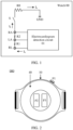
- FIG. 2 is a schematic diagram of a structure of an electrocardiogram detection device according to an embodiment of this application
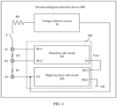
- FIG. 3 is an equivalent circuit diagram of an electrocardiogram detection device according to an embodiment of this application.
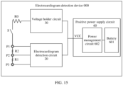
- the electrocardiogram detection device 000 may include a housing 10 made of a conductive material, an electrocardiogram detection circuit 20 and a voltage holder circuit 30 that are disposed in the housing 10, and a first electrode P1, a second electrode P2, and a third electrode P3 that are disposed outside the housing 10 and insulated from the housing 10.
- the first electrode P1, the second electrode P2, and the third electrode P3 are exposed outside the housing 10, to facilitate contact with skin of a user.
- the second electrode P2 and the third electrode P3 may be located on a first outer surface of the electrocardiogram detection device 000, the first electrode P1 may be located on a second outer surface of the electrocardiogram detection device 000, and the first outer surface and the second outer surface are different outer surfaces of the electrocardiogram detection device 000.
- the electrocardiogram detection device 000 is a watch shown in FIG. 2 .
- the first outer surface may be an outer surface of a bottom cover 40 of the watch
- the second outer surface may be an outer surface of the housing 10 (that is, a watch housing) of the watch.
- the first electrode P1 may be disposed on a watch crown of the watch.
- the electrocardiogram detection circuit 20 may be separately connected to the first electrode P1, the second electrode P2, and the third electrode P3.
- the electrocardiogram detection circuit 20 may be configured to collect an electrocardiogram signal by using the first electrode P1 and the second electrode P2, and provide a reference potential for the third electrode P3.
- the electrocardiogram detection circuit 20 may provide the reference potential for the human body by using the third electrode P3. This ensures reliability of the electrocardiogram signal collected by the electrocardiogram detection circuit 20 by using the first electrode P1 and the second electrode P2.
- the voltage holder circuit 30 is connected to the housing 10 (the housing 10 is equivalent to a resistor R0 in FIG. 3 ).
- the connection may be a direct connection or an indirect connection. That is, the voltage holder circuit 30 may alternatively be connected to the housing 10 by using another electronic component (for example, a resistor).
- the voltage holder circuit 30 is configured to provide a target potential for the housing 10. A potential difference between the target potential and the reference potential is less than a difference threshold. That is, the voltage holder circuit 30 may enable a potential of the housing 10 to be equal to or approximately equal to the reference potential.
- the difference threshold may be flexibly set based on a requirement of an actual application scenario when process precision permits.
- an order of magnitude of the difference threshold may be a microvolt (uv) level or a millivolt (mv) level.
- the target potential is equal to or close to the reference potential.
- the target potential being equal to or close to the reference potential means that the potential difference between the target potential and the reference potential is controlled within an error range allowed by engineering specifications.
- the target potential and the reference potential may be the same or close, that is, may be completely the same. However, because it is difficult to implement in practice, it may not be required that the target potential and the reference potential be completely the same, and a specific error may be allowed. For example, if a voltage difference between the target potential and the reference potential is a specific value (for example, 10 uv), but a leakage current can be suppressed at this time, and the potential difference meets engineering specification requirements of the product, this design is also acceptable.
- an order of magnitude of the error range may be an uv level or an mv level.
- an embodiment of this application provides an electrocardiogram detection device.
- a housing of the electrocardiogram detection device may be made of a conductive material.
- the electrocardiogram detection device may include a voltage holder circuit configured to provide a target potential for the housing.
- a potential difference between the target potential provided by the voltage holder circuit and a reference potential provided by the electrocardiogram detection circuit for a third electrode is small. Therefore, in an ECG detection process, even if a user accidentally touches the housing and causes the housing to be conducted to the third electrode, no leakage current is generated between the housing and the third electrode or a small leakage current is generated between the housing and the third electrode. This can effectively reduce interference to an ECG signal and ensure accuracy of ECG detection.
- a requirement on insulation performance of the housing of the electrocardiogram detection device is low. That is, a requirement on insulation performance of an insulation material coated on a surface of the housing is low. Therefore, a higher-cost process is not required to achieve better insulation performance of the housing. This avoids an increase in the production cost of the housing.
- the first electrode P1, the second electrode P2, and the third electrode P3 may all be dry electrodes.
- the dry electrode is an electrode that does not need to be used with a conductive paste.
- the voltage holder circuit 30 may include an output end, and the output end is connected to the housing 10.
- the voltage holder circuit 30 may include one or more input ends.
- the one or more input ends are connected to one or more potential providers in a one-to-one correspondence.
- the voltage holder circuit 30 is configured to output the target potential at the output end of the voltage holder circuit 30 based on an input signal of the input end of the voltage holder circuit 30. That is, the voltage holder circuit 30 may output the target potential after processing received one or more input signals.
- there is one potential provider and may specifically be the third electrode P3, or the second electrode P2, or the first electrode P1, or a power supply output end.
- the potential provider is the third electrode P3.
- FIG. 4 is an equivalent circuit diagram of another electrocardiogram detection device according to an embodiment of this application.
- the electrocardiogram detection circuit 20 may include a detection sub-circuit 201 and a right leg drive sub-circuit 202.
- a first input end IN11 of the detection sub-circuit 201 is connected to the first electrode P1.
- a second input end IN 12 of the detection sub-circuit 201 is connected to the second electrode P2.
- a common-mode output end O1 of the detection sub-circuit 201 is connected to a first input end IN21 of the right leg drive sub-circuit 202.
- the detection sub-circuit 201 is configured to collect an electrocardiogram signal, and output a common-mode voltage Vcm between the first input end IN11 and a second input end IN22 to the right leg drive sub-circuit 202.
- the second input end IN22 of the right leg drive sub-circuit 202 is connected to a reference power supply end VR.
- An output end O2 of the right leg drive sub-circuit 202 is connected to the third electrode P3.
- the right leg drive sub-circuit 202 is configured to provide a reference potential for the third electrode P3 under driving of the common-mode voltage Vcm and the reference power supply end VR.
- the right leg drive sub-circuit 202 serves as a negative feedback circuit, and can provide a reference potential for the third electrode after inverting and amplifying a received common-mode voltage, to eliminate common-mode interference of a human body.
- FIG. 5 is an equivalent circuit diagram of still another electrocardiogram detection device according to an embodiment of this application.
- the detection sub-circuit 201 may include an instrumentation amplifier (instrumentation amplifier, INA), an analog-to-digital converter (analogue-to-digital conversion, ADC), and a processor 2011.
- the right leg drive sub-circuit 202 may include a second operational amplifier AMP2.
- An out-of-phase input end of the INA serves as a first input end IN11 of the detection sub-circuit 201, and may be connected to the first electrode P1.
- An in-phase input end of the INA serves as a second input end IN12 of the detection sub-circuit 201, and may be connected to the second electrode P2.
- a common-mode output end of the INA serves as a common-mode output end O1 of the detection sub-circuit 201, and may be connected to an out-of-phase input end of the second operational amplifier AMP2 (that is, a first input end IN21 of the right leg drive sub-circuit 202), and a differential-mode output end of the INA may be connected to an input end of the ADC.
- the INA may collect a potential of the in-phase input end and a potential of the out-of-phase input end of the INA, output a differential-mode voltage Vdm (the differential-mode voltage Vdm is an ECG signal) between the in-phase input end and the out-of-phase input end by using the differential-mode output end, and output a common-mode voltage Vcm between the in-phase input end and the out-of-phase input end by using the common-mode output end.
- Vdm the differential-mode voltage Vdm is an ECG signal
- the INA has advantages such as a low direct-current offset, a low drift, low noise, a high open-loop gain, a larger common-mode rejection ratio, and a high input impedance, and can be applied to an electrocardiogram detection circuit 20 that has a high requirement on accuracy and stability.
- An output end of the ADC is connected to the processor 2011.
- the ADC is configured to: perform analog-to-digital conversion on the differential-mode voltage Vdm output by the INA to obtain a digital signal, and send the digital signal to the processor 2011.
- the processor 2011 may further process the digital signal to generate an ECG.
- the processor 2011 may be a micro-controller unit (micro-controller unit, MCU), or may be a digital signal processor (digital signal processor, DSP), or various other processing circuits having a signal processing capability.
- MCU micro-controller unit
- DSP digital signal processor
- An in-phase input end of the second operational amplifier AMP2 serves as a second input end IN22 of the right leg drive sub-circuit 202 and is connected to a reference power supply end VR.
- An output end of the second operational amplifier AMP2 serves as an output end O2 of the right leg drive sub-circuit 202 and is connected to the third electrode P3.
- the detection sub-circuit 201 may further include another electronic component, for example, may further include a filter or another functional circuit.
- the right leg drive sub-circuit 202 may further include electronic components such as a resistor and a capacitor, or may further include another operational amplifier cascaded to the second operational amplifier AMP2. Circuit structures of the detection sub-circuit 201 and the right leg drive sub-circuit 202 are not limited in this embodiment of this application.
- the electrocardiogram detection device 000 may supply power to each electronic component by using a positive power supply circuit.
- the positive power supply circuit has a power supply output end VCC configured to provide a system positive potential Vcc for the electrocardiogram detection circuit.
- a positive power supply electrode of each electronic component may be connected to the power supply output end VCC, and a negative power supply electrode may be directly grounded.
- this power supply mode is also called single-power supply mode, which is different from the dual-power supply mode in which both positive and negative power supplies are used.
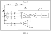
- FIG. 6 is an equivalent circuit diagram of a watch having an ECG detection function in the related technology.
- a system positive potential provided by the positive power supply circuit is Vcc
- a potential of an out-of-phase input end of the INA is V1
- a potential of an in-phase input end of the INA is V2
- the common-mode voltage Vcm between the in-phase input end and the out-of-phase input end of the INA may be kept in a range approximately equal to the potential Vref of the reference power supply end VR.
- a contact impedance Z1 and a half-battery voltage e1 are generated on a contact surface between the human skin and the first electrode P1
- a contact impedance Z2 and a half-battery voltage e2 are generated on a contact surface between the skin and the second electrode P2
- a contact impedance Z3 and a half-battery voltage e3 are generated on a contact surface between the skin and the third electrode P3.
- the electrode is metal, but the skin of the human body is non-metal. Therefore, after the skin is in contact with the electrode, the contact surface between the skin and the electrode interact with each other to generate a voltage, and the voltage is the half-battery voltage.
- a potential of the human body is V0 (which is generally approximately equal to Vcc/2 according to an experiment), and an ECG signal generated by the human body and internal resistances R1 and R2 of the human body are ignored.
- sweat generated by the human body may also cause the third electrode P3 to be conducted to the housing, so that the leakage current I b is generated between the output end of the second operational amplifier AMP2 and the housing.
- an electrochemical reaction occurs under an action of the leakage current I b on the housing and the electrode that are infiltrated by sweat, or another metal component (for example, a screw) that is infiltrated by sweat and that is electrically connected to the housing, and corrosion occurs.
- a larger leakage current I b indicates a faster corrosion speed.
- a voltage holder circuit 30 provides a target potential for the housing 10, so that a potential difference between the potential of the housing 10 and the reference potential V3 provided by an electrocardiogram detection circuit 20 for the third electrode P3 can be small. Therefore, even if the housing 10 is conducted to the third electrode P3 due to an accidental touch of the user or sweat infiltration, no leakage current is generated between the housing 10 and the third electrode P3 or a small leakage current is generated between the housing 10 and the third electrode P3. This can ensure accuracy of ECG detection.
- the voltage holder circuit 30 may be a voltage follower circuit.
- An input end of the voltage follower circuit 30 serves as an input end of the voltage holder circuit and is connected to a potential provider, and an output end of the voltage follower circuit 30 serves as an output end of the voltage holder circuit and is connected to the housing 10.
- the voltage follower circuit 30 is configured to follow a potential of the input end (connected to the potential provider) of the voltage follower circuit 30, so that a potential of the output end (output to the housing) of the voltage follower circuit 30 is consistent with the potential of the input end as much as possible. In this way, the potential of the housing 10 can be controlled to be substantially consistent with the target potential of the potential provider.
- the potential provider may be the third electrode P3, that is, the output end O2 of the right leg drive sub-circuit 202, or the output end of the second operational amplifier AMP2.
- the voltage follower circuit 30 may control the potential of the housing 10 to be substantially consistent with the reference potential V3 of the output end of the second operational amplifier AMP2, that is, the target potential is the reference potential V3.
- the potential provider may be the first electrode P1, that is, the first input end IN11 of the detection sub-circuit 201, or the out-of-phase input end of the INA.
- the voltage follower circuit 30 may control the potential of the housing 10 to be substantially consistent with the potential of the out-of-phase input end of the INA. That is, the target potential is V1.
- the potential provider may be the second electrode P2, that is, the second input end IN12 of the detection sub-circuit 201, or the in-phase input end of the INA.
- the voltage follower circuit 30 may control the potential of the housing 10 to be substantially consistent with the potential of the in-phase input end of the INA. That is, the target potential is V2.
- the potential provider may be the common-mode output end O1 of the detection sub-circuit 201, that is, the common-mode output end of the INA.
- the voltage follower circuit 30 may control the potential of the housing 10 to be substantially consistent with the potential of the common-mode output end O1 of the INA. That is, the target potential is Vcm.
- the potential provider may alternatively be the out-of-phase input end of the second operational amplifier AMP2.
- the voltage follower circuit 30 has a voltage following function, so that the potential of the housing 10 can be controlled to be substantially consistent with the target potential of the potential provider.
- the potential of the housing 10 being controlled to be substantially consistent with the target potential of the potential provider means that the potential difference between the potential of the housing 10 and the target potential of the potential provider is controlled within an error range allowed by engineering specifications. Complete consistency may not be required, and a specific error may be allowed. For example, if a voltage difference between the target potential and the reference potential is a specific value (for example, 10 uv), but a leakage current can be suppressed at this time, and the potential difference meets engineering specification requirements of the product, this design is also acceptable.
- an order of magnitude of the error range may be an uv level or an mv level.
- the potential provider is the third electrode P3, that is, when the target potential is the reference potential V3, the potential of the housing 10 is consistent with the potential of the third electrode P3. Therefore, even if the third electrode P3 is conducted to the housing 10, no leakage current is generated between the third electrode P3 and the housing 10. In this case, suppression on the leakage current is better.
- FIG. 10 is a schematic diagram of potentials of terminals in an electrocardiogram detection circuit according to an embodiment of this application.
- a longitudinal axis in FIG. 10 represents a potential value, and a horizontal axis has no actual meaning.
- the voltage follower circuit 30 may include a first operational amplifier AMP 1.
- An in-phase input end of the first operational amplifier AMP1 serves as an input end of the voltage follower circuit 30 and may be connected to the potential provider.
- An output end of the first operational amplifier AMP1 serves as an output end of the voltage follower circuit 30 and may be separately connected to the housing 10 (that is, the equivalent resistance R0 shown in FIG. 5 and FIG. 7 to FIG. 9 ) and an out-of-phase input end of the first operational amplifier AMP1.
- the output end of the first operational amplifier AMP1 may be indirectly connected to the housing 10.
- the output end of the first operational amplifier AMP1 is connected to the housing 10 by using a resistor R3.
- the output end of the first operational amplifier AMP1 is connected to the out-of-phase input end, so that a potential of the output end of the first operational amplifier AMP 1 changes with a potential of the in-phase input end. That is, voltage following can be implemented.
- an input resistance of the first operational amplifier AMP1 is high (the input resistance is infinite in an ideal case), impact on the potential of the potential provider can be avoided, and it is ensured that a detection sub-circuit 201 and a right leg drive sub-circuit 202 can run normally.
- the first operational amplifier AMP1 may have three ports in total: an in-phase input end, an out-of-phase input end, and an output end.
- the three ports may be separately connected to corresponding components.
- the first operational amplifier AMP1 may also be packaged as a component having only two ports in total: an in-phase input end and an output end. That is, the out-of-phase input end of the first operational amplifier AMP1 is already connected to the output end before packaging.
- the first operational amplifier AMP1 may also be referred to as a voltage buffer.
- the in-phase input end and the output end need only to be separately connected to corresponding components.
- the voltage follower circuit 30 may include a plurality of cascaded first operational amplifiers AMP1.
- the voltage follower circuit 30 may include a plurality of cascaded discrete triodes.
- the plurality of cascaded triodes can implement a function of an operational amplifier, and further implement voltage following. How to specifically use the plurality of cascaded triodes to implement a function of the operational amplifier is a conventional technology in the art, and details are not described in this application.
- each component (such as an AMP or an ADC) is merely used to represent a logic circuit having the function.
- one or more circuits may be packaged into one chip, to increase integration and reduce a volume.
- the INA and the second operational amplifier AMP2 in the detection sub-circuit 201 may be integrated into one chip, and the chip may also be referred to as an ECG chip.
- Pins of the ECG chip may include at least a first input pin (that is, the out-of-phase input end of the INA) configured to connect to the first electrode P1, a second input pin (that is, the in-phase input end of the INA) configured to connect to the second electrode P2, and an output pin (that is, the output end of the AMP2) configured to connect to the third electrode P3.
- the ECG chip may further include other pins, for example, a pin configured to ground, and a pin configured to connect to the reference power supply end VR.
- the in-phase input end of the first operational amplifier AMP 1 may be externally connected to the first input pin, the second input pin, or the output pin of the ECG chip.
- the first operational amplifier AMP1 is connected to the first input pin, the second input pin, or the output pin of the ECG chip, so that a conventional ECG chip can also be applied to the electrocardiogram detection device provided in this embodiment of this application. This effectively improves compatibility of the electrocardiogram detection device.
- the INA, the second operational amplifier AMP2, and the first operational amplifier AMP 1 in the detection sub-circuit 201 may all be integrated into an ECG chip.
- pins of the ECG chip may further include an output pin configured to connect to the housing 10.
- the INA, the AMP2, and the AMP1 are all integrated into the ECG chip, so that integration of electronic components in the electrocardiogram detection device can be effectively improved, and a volume of the electronic component can be reduced.
- the INA, the second operational amplifier AMP2, the ADC, and the first operational amplifier AMP1 in the detection sub-circuit 201 may all be integrated into an ECG chip.
- the INA, the second operational amplifier AMP2, the ADC, a processor 2011, and the first operational amplifier AMP1 in the detection sub-circuit 201 may all be integrated into an ECG chip.
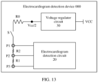
- the voltage holder circuit 30 is a voltage regulator circuit, and the voltage regulator circuit may also be referred to as a voltage regulator (regulator), that is, configured to output a stable voltage when an input changes.
- An input end of the voltage regulator circuit 30 serves as an input end of the voltage holder circuit and may be connected to a power supply output end VCC.
- An output end of the voltage regulator circuit 30 serves as an output end of the voltage holder circuit and is connected to the housing 10 (that is, an equivalent resistance R0 shown in FIG. 13 ).
- the voltage regulator circuit 30 may be configured to provide the target potential for the housing 10 under driving of the power supply output end VCC.
- the voltage regulator circuit 30 is used to provide the target potential.
- a potential of the power supply output end VCC may be properly designed, so that the target potential provided by the voltage regulator circuit 30 for the housing 10 is approximately equal to the reference potential. This can ensure suppression on a leakage current.
- the target potential provided by the voltage regulator circuit 30 for the housing 10 may be equal to the potential Vref of the reference power supply end VR.
- the target potential provided by the voltage regulator circuit 30 for the housing 10 may be Vcc/2.
- FIG. 14 is an equivalent circuit diagram of still another electrocardiogram detection device according to an embodiment of this application.
- the voltage regulator circuit 30 may be an LDO.
- the LDO has advantages such as low noise and a small static current.
- the electrocardiogram detection device 000 may further include a resistor R3 disposed in the housing 10 and connected in series between the housing 10 and the output end (for example, an output end of the voltage follower circuit or an output end of the voltage regulator circuit) of the voltage holder circuit 30.
- a resistor R3 disposed in the housing 10 and connected in series between the housing 10 and the output end (for example, an output end of the voltage follower circuit or an output end of the voltage regulator circuit) of the voltage holder circuit 30.
- the resistor R3 is connected in series between the housing 10 and the output end of the voltage holder circuit 30, so that a resistance on a path of the leakage current can be further increased, and the leakage current can be effectively reduced. This can further reduces a baseline drift of the ECG as much as possible, and ensure reliability of ECG detection.
- the electrocardiogram detection device 000 may further include a capacitor C disposed in the housing 10 and connected in parallel to the resistor R3.
- the capacitor C connected in parallel and a resistor R2 may also be referred to as a resistor-capacitor network.
- the capacitor C can effectively resist electromagnetic interference (electromagnetic interference, EMI) and electrostatic discharge (electrostatic discharge, ESD).
- a resistance value of the resistor R3 and a capacitance value of the capacitor C may be flexibly set based on a requirement of an application scenario.
- the electrocardiogram detection device 000 is a wearable device such as a watch or a band
- an order of magnitude of a resistance value of the resistor R3 may be a megaohm (M ⁇ ) level
- an order of magnitude of a capacitance value of the capacitor C may be a picofarad (pF) level.
- a resistance value of the resistor R3 may be 10 MS2
- a capacitance value of the capacitor C may be 47 pF.
- the electrocardiogram detection device 000 may further include an ESD circuit 50 disposed in the housing 10. One end of the ESD circuit 50 may be connected to the housing 10, and the other end may be grounded.
- the ESD circuit 50 can prevent each component in the electrocardiogram detection device 000 from being damaged due to ESD impact. This can effectively improve ESD performance of the electrocardiogram detection device.
- the ESD circuit 50 may include a diode, for example, may include a TVS.
- One electrode of the TVS may be connected to the housing 10, and the other electrode may be grounded.
- the TVS has advantages of a fast response, a high transient power, a small leakage current, a small breakdown voltage deviation, easy control of clamping voltage, no damage limit, and a small size.
- the TVS can effectively protect each component in the electrocardiogram detection device, and prevent each component from being damaged by a surge pulse.
- the electrocardiogram detection device 000 provided in this embodiment of this application may further include a positive power supply circuit 60 disposed in the housing 10.
- the positive power supply circuit 60 has a power supply output end VCC.
- the positive power supply circuit 60 may supply power to the electrocardiogram detection circuit 20 and the voltage holder circuit 30 by using the power supply output end VCC.
- a circuit (for example, the INA and the second operational amplifier AMP2 shown in FIG. 5 , FIG. 7 to FIG. 9 , and FIG. 14 ) that is in the electrocardiogram detection circuit 20 and that is connected before an input end of the ADC may be referred to as an analog front end (analog front end, AFE).
- the AFE may amplify a coupled analog signal (that is, an ECG signal), and send the analog signal to the ADC for analog-to-digital conversion processing.
- the positive power supply circuit 60 provided in this embodiment of this application may provide a single power supply for the AFE in the electrocardiogram detection circuit 20 and the voltage holder circuit 30.
- the single power supply means that a type of power supply (for example, a positive power supply) is used to power an analog circuit, to distinguish from dual power supplies formed by positive and negative power supplies.
- the single power supply is usually powered by a positive power supply.
- a positive power supply for example, a 1.8 V power supply or a 2.5 V power supply
- the positive power supply circuit 60 may include two outputs. One outputs Vcc (for example, 1.8 V), and the other outputs Vcc/2.
- a power supply mode of a digital circuit (such as an ADC and a processor) in the electrocardiogram detection circuit 20 is not limited, and various existing power supply modes may be used for power supply.
- the power supply circuit 60 may alternatively supply power.
- the positive power supply circuit 60 includes a battery 601 and a power management circuit 602.
- the power management circuit 602 may be a power management integrated circuit (power management integrated circuit, PMIC).
- the power management circuit 602 may convert a potential provided by the battery 601 into a system positive potential Vcc, and then output the system positive potential Vcc to the power supply output end VCC.
- the potential provided by the battery 601 may be 3.8 V.
- the power management circuit 602 may convert the potential of 3.8 V into 1.8 V or 2.5 V, and then provide the 1.8 V or 2.5 V potential to the power supply output end VCC. That is, the system positive potential Vcc provided by the power supply output end VCC is 1.8 V or 2.5 V.
- the electrocardiogram detection circuit 20 may further include a voltage conversion circuit (not shown in the figure), and the voltage conversion circuit is separately connected to the power supply output end VCC and the reference power supply end VR.
- the voltage conversion circuit may convert the system positive potential Vcc output by the power supply output end VCC into Vcc/2, and then provide the Vcc/2 to the reference power supply end VR.
- the voltage conversion circuit may be integrated into an ECG chip. Implementation of the voltage conversion circuit is the conventional technology, and details are not described in this application.
- a circuit structure of the positive power supply circuit is simple, and costs are low. Therefore, the positive power supply circuit is used in the electrocardiogram detection device provided in this embodiment of this application. This can effectively reduce complexity of the circuit structure of the electrocardiogram detection device and costs of the entire system.
- the positive power supply circuit 60 may provide the system positive potential Vcc for the first operational amplifier AMP1 or the LDO in the voltage holder circuit 30 by using the power supply output end VCC, and provide the system positive potential Vcc for the INA in the electrocardiogram detection circuit 20.
- the electrocardiogram detection device 000 provided in this embodiment of this application may be a wearable device.
- the device may be a wrist-wearing device such as a watch, a band, or an anklet, or may be an armband device, or may be smart glasses or a head-mounted display device.
- the wearable device such as the watch or the band is used as the electrocardiogram detection device, so that the user can detect an electrocardiogram signal of the user in real time. This improves flexibility of electrocardiogram signal detection.
- the housing 10 may be a watch housing (which may also be referred to as a middle frame) of the watch or the band.
- the watch or the band may further include a bottom cover 40 and a display screen 70.
- the watch housing 10, the bottom cover 40, and the display screen 70 may form a closed cavity.
- the electrocardiogram detection circuit 20 and the voltage holder circuit 30 may be disposed in the cavity.
- the display screen 70 may be a touch display screen.
- the second electrode P2 and the third electrode P3 may be disposed on an outer side of the bottom cover 40, that is, a side that is of the bottom cover 40 and that is away from the display screen 70.
- the first electrode P1 may be disposed on an outer side of the watch housing 10.
- a watch crown 80 may be disposed on an outer side of the watch housing 10, and the first electrode P1 may be disposed on the watch crown 80.
- the second electrode P2 and the third electrode P3 may be in contact with skin of the wrist of the user.
- the user may touch the first electrode P1 with a finger of another hand (for example, a finger of the right hand), and the electrocardiogram detection circuit 20 may further collect an electrocardiogram signal of the user by using the first electrode P1 and the second electrode P2.
- an embodiment of this application provides an electrocardiogram detection device.
- a housing of the electrocardiogram detection device may be made of a conductive material.
- the electrocardiogram detection device may include a voltage holder circuit configured to provide a target potential for the housing.
- a potential difference between the target potential provided by the voltage holder circuit and a reference potential provided by the electrocardiogram detection circuit for a third electrode is small. Therefore, in an ECG detection process, even if a user accidentally touches the housing and causes the housing to be conducted to the third electrode, no leakage current is generated between the housing and the third electrode or a small leakage current is generated between the housing and the third electrode. This can effectively reduce interference to an ECG signal and ensure accuracy of ECG detection.
- the potential difference between the housing and the third electrode may be reduced by adding the voltage holder circuit. Therefore, a requirement on insulation performance of the housing of the electrocardiogram detection device can be lowered. In this way, impact of accidental finger touch or sweat infiltration on ECG detection can be effectively reduced without changing a production process of the housing of the entire system and a power supply architecture of the electrocardiogram detection circuit.
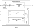
- an embodiment of this application further provides a detection circuit 0000 applied to an electrocardiogram detection device.
- the electrocardiogram detection device includes a housing made of a conductive material.
- the detection circuit 0000 includes a first input pin 11, a second input pin J2, a first output pin J3, and a second output pin J4.
- the first input pin J1 is configured to connect to a first electrode.
- the second input pin J2 is configured to connect to a second electrode.
- the first output pin J3 is configured to connect to a third electrode.
- the detection circuit 0000 is configured to collect an electrocardiogram signal by using the first input pin J1 and the second input pin J2, and provide a reference potential for the third electrode by using the first output pin J3.
- the first electrode, the second electrode, and the third electrode are all disposed outside the housing of the electrocardiogram detection device, and are insulated from the housing.
- the second output pin J4 is configured to connect to the housing of the electrocardiogram detection device.
- the detection circuit 0000 is further configured to provide a target potential for the housing by using the second output pin J4.
- a potential difference between the target potential and the reference potential is less than a difference threshold.
- the target potential is equal to or close to the reference potential.
- the detection circuit 0000 further includes a circuit configured to collect an electrocardiogram signal, a circuit configured to provide a reference potential, and a circuit configured to provide a target potential.
- the detection circuit 0000 may include a voltage holder circuit 100.
- An output end O3 of the voltage holder circuit 100 is connected to the second output pin J4.
- An input end IN3 of the voltage holder circuit 100 is configured to connect to a potential provider.
- the voltage holder circuit 100 is configured to output the target potential at the output end O3 based on an input signal of the input end IN3.
- the detection circuit 0000 further includes a power supply pin J5.
- the power supply pin J5 is configured to connect to a power supply output end VCC.
- the potential provider connected to the input end IN3 of the voltage holder circuit 100 may be the first electrode, or the second electrode, or the third electrode, or the power supply output end VCC.
- the potential provider is the first electrode, or the second electrode, or the third electrode.
- the voltage holder circuit 100 is a voltage follower circuit.
- An output end O3 of the voltage follower circuit 100 serves as the output end of the voltage holder circuit and is connected to the second output pin 14, and an input end IN3 of the voltage follower circuit 100 is configured to connect to the potential provider.
- the input end IN3 of the voltage follower circuit 100 shown in FIG. 7 serves as the input end of the voltage holder circuit and is connected to the first output pin J3. That is, the input end IN3 of the voltage follower circuit 100 is configured to connect to the third electrode.
- the voltage follower circuit 100 is configured to control a potential of the second output pin J4 to be substantially consistent with the target potential of the potential provider.
- the detection circuit 0000 further includes an electrocardiogram detection circuit 200.
- the electrocardiogram detection circuit 200 may include a detection sub-circuit 2001 and a right leg drive sub-circuit 2002.
- a first input end IN 11 of the detection sub-circuit 2001 is connected to the first input pin 11.
- a second input end IN12 of the detection sub-circuit 2001 is connected to the second input pin J2.
- a common-mode output end O1 of the detection sub-circuit 2001 is connected to a first input end IN21 of the right leg drive circuit 200.
- the detection sub-circuit 2001 is configured to collect an electrocardiogram signal, output a common-mode voltage between the first input end IN 11 and the second input end IN 12 to the right leg drive sub-circuit 2002.
- a second input end IN22 of the right leg drive sub-circuit 2002 is connected to a reference power supply end VR.
- An output end O2 of the right leg drive sub-circuit 2002 is connected to the first output pin J3.
- the right leg drive sub-circuit 2002 is configured to provide the reference potential for the first output pin J3 under driving of the common-mode voltage and the reference power supply end VR.
- the potential provider connected to the input end IN3 of the voltage follower circuit 100 may be the common-mode output end O1 of the detection sub-circuit 2001.
- a structure of the detection sub-circuit 2001 may be the same as a structure of the detection sub-circuit 201 in the foregoing embodiment, and a structure of the right leg drive sub-circuit 2002 may be the same as a structure of the right leg drive sub-circuit 202 in the foregoing embodiment. Therefore, details are not described herein again.
- the detection circuit 0000 may further include a voltage conversion circuit, and the voltage conversion circuit is separately connected to the power supply pin J5 and the reference power supply end VR.
- the voltage conversion circuit may convert the system positive potential Vcc output by the power supply output end VCC connected to the power supply pin J5 into Vcc/2, and then provide the Vcc/2 to the reference power supply end VR.
- the voltage follower circuit 100 may include a first operational amplifier AMP1.
- An in-phase input end of the first operational amplifier AMP1 serves as the input end of the voltage follower circuit 100 and is connected to the potential provider.
- An output end of the first operational amplifier AMP1 serves as the output end of the voltage follower circuit 100 and is separately connected to the second output pin J4 and an out-of-phase input end of the first operational amplifier AMP1.
- the potential provider is the power supply output end VCC.
- the voltage holder circuit 100 is a voltage regulator circuit. As shown in FIG. 18 , an input end IN3 of the voltage regulator circuit 100 serves as the input end of the voltage holder circuit and is connected to the power supply pin J5. An output end O3 of the voltage regulator circuit 100 serves as the output end of the voltage holder circuit and is connected to the second output pin J4.
- the voltage regulator circuit 100 is configured to provide the target potential for the second output pin J4 under driving of the power supply output end VCC connected to the power supply pin J5.
- the voltage regulator circuit may be an LDO.
- the detection circuit 0000 may further include a resistor R3 connected in series between the second output pin J4 and the voltage holder circuit 100.
- the detection circuit 0000 further includes a capacitor C connected in parallel to the resistor R3.
- the detection circuit 0000 further includes an ESD circuit 300.
- One end of the ESD circuit 300 is connected to the second output pin 14, and the other end is grounded.
- the ESD circuit 300 includes a TVS.
- One electrode of the TVS is connected to the second output pin 14, and the other electrode of the TVS is grounded.
- the detection circuit may be an integrated circuit (integrated circuit, IC), and circuits included in the detection circuit may be packaged in a single chip. Because a volume of the packaged chip is small, an increase in a volume of an electrocardiogram detection device using the chip can be avoided. That is, the detection circuit may be applied to a small electrocardiogram detection device.
- IC integrated circuit
- an embodiment of this application provides a detection circuit applied to an electrocardiogram detection device.
- a potential difference between a target potential provided by the detection circuit for a housing of the electrocardiogram detection device and a reference potential provided for a third electrode of the electrocardiogram detection device is small. Therefore, in an ECG detection process, even if a user accidentally touches the housing and causes the housing to be conducted to the third electrode, no leakage current is generated between the housing and the third electrode or a small leakage current is generated between the housing and the third electrode. This can effectively reduce interference to an ECG signal and ensure accuracy of ECG detection.
- the protection scope of this invention shall be subject to the protection scope of the claims.
Landscapes
- Health & Medical Sciences (AREA)
- Life Sciences & Earth Sciences (AREA)
- Medical Informatics (AREA)
- Biophysics (AREA)
- Pathology (AREA)
- Engineering & Computer Science (AREA)
- Biomedical Technology (AREA)
- Heart & Thoracic Surgery (AREA)
- Physics & Mathematics (AREA)
- Molecular Biology (AREA)
- Surgery (AREA)
- Animal Behavior & Ethology (AREA)
- General Health & Medical Sciences (AREA)
- Public Health (AREA)
- Veterinary Medicine (AREA)
- Cardiology (AREA)
- Measurement And Recording Of Electrical Phenomena And Electrical Characteristics Of The Living Body (AREA)
Claims (11)
- Elektrokardiogramm-Erkennungsvorrichtung, wobei die Vorrichtung ein Gehäuse (10) aus einem leitfähigen Material, eine Elektrokardiogramm-Erkennungsschaltung (0, 1, 20, 200) und eine Spannungshalterschaltung (30, 100), die im Gehäuse (10) angeordnet sind, sowie eine erste Elektrode (P1), eine zweite Elektrode (P2) und eine dritte Elektrode (P3) umfasst, die außerhalb des Gehäuses (10) angeordnet sind und von dem Gehäuse (10) isoliert sind;die Elektrokardiogramm-Erkennungsschaltung (0, 1, 20, 200) separat mit der ersten Elektrode (P1), der zweiten Elektrode (P2) und der dritten Elektrode (P3) verbunden ist, und die Elektrokardiogramm-Erkennungsschaltung (0, 1, 20, 200) dazu konfiguriert ist, ein Elektrokardiogrammsignal unter Verwendung der ersten Elektrode (P1) und der zweiten Elektrode (P2) zu erfassen und ein Referenzpotenzial für die dritte Elektrode (P3) bereitzustellen; unddie Spannungshalterschaltung (30, 100) mit dem Gehäuse (10) verbunden ist und dazu konfiguriert ist, ein Zielpotenzial für das Gehäuse (10) bereitzustellen, wobei eine Potenzialdifferenz zwischen dem Zielpotenzial und dem Referenzpotenzial geringer ist als ein Differenzschwellenwert;wobei ein Ausgangsende der Spannungshalterschaltung (30, 100) mit dem Gehäuse (10) verbunden ist, ein Eingangsende der Spannungshalterschaltung (30, 100) mit einem Potenzialbereitsteller verbunden ist und die Spannungshalterschaltung (30, 100) dazu konfiguriert ist, das Zielpotenzial an dem Ausgangsende basierend auf einem Eingangssignal des Eingangsendes auszugeben;wobei die Elektrokardiogramm-Erkennungsschaltung (0, 1, 20, 200) eine Erkennungs-Unterschaltung (201, 2001) und eine Neutralelektroden-Unterschaltung (202, 2002) umfasst;ein erstes Eingangsende der Erkennungsunterschaltung (201, 2001) mit der ersten Elektrode verbunden ist, ein zweites Eingangsende der Erkennungsunterschaltung (201, 2001) mit der zweiten Elektrode verbunden ist, ein Gleichtaktausgangsende der Erkennungsunterschaltung (201, 2001) mit einem ersten Eingangsende der Neutralelektroden-Unterschaltung (202, 2002) verbunden ist, und die Erkennungsunterschaltung (201, 2001) dazu konfiguriert ist, ein Elektrokardiogrammsignal zu erfassen und eine Gleichtaktspannung zwischen dem ersten Eingangsende und dem zweiten Eingangsende an die Neutralelektroden-Unterschaltung (202, 2002) auszugeben; undein zweites Eingangsende der Neutralelektroden-Unterschaltung (202, 2002) mit einem Referenzstromversorgungsende verbunden ist, ein Ausgangsende der Neutralelektroden-Unterschaltung (202, 2002) mit der dritten Elektrode verbunden ist und die Neutralelektroden-Unterschaltung (202, 2002) dazu konfiguriert ist, unter Ansteuerung der Gleichtaktspannung und des Referenzstromversorgungsendes ein Referenzpotenzial für die dritte Elektrode bereitzustellen, wobeider Potenzialbereitsteller die dritte Elektrode oder die zweite Elektrode oder die erste Elektrode oder das Gleichtaktausgangsende ist; undwobei die Erkennungsunterschaltung (201, 2001) einen Instrumentenverstärker, einen Analog-Digital-Wandler und einen Prozessor (2011) umfasst; und die Neutralelektroden-Unterschaltung (202, 2002) einen zweiten Operationsverstärker umfasst;ein gegenphasiges Eingangsende des Instrumentenverstärkers als das erste Eingangsende der Erkennungsunterschaltung (201, 2001) dient und mit der ersten Elektrode verbunden ist, ein gleichphasiges Eingangsende des Instrumentenverstärkers als das zweite Eingangsende der Erkennungsunterschaltung (201, 2001) dient und mit der zweiten Elektrode verbunden ist, ein Gleichtaktausgangsende des Instrumentenverstärkers als Gleichtaktausgangsende der Erkennungsunterschaltung (201, 2001) dient und mit einem gegenphasigen Eingangsende des zweiten Operationsverstärkers verbunden ist, ein Differenzmodusausgangsende des Instrumentenverstärkers mit einem Eingangsende des Analog-Digital-Wandlers verbunden ist und das gegenphasige Eingangsende des zweiten Operationsverstärkers das erste Eingangsende der Neutralelektroden-Unterschaltung (202, 2002) ist;ein Ausgangsende des Analog-Digital-Wandlers mit dem Prozessor (2011) verbunden ist; undein gleichphasiges Eingangsende des zweiten Operationsverstärkers als das zweite Eingangsende der Neutralelektroden-Unterschaltung (202, 2002) dient und mit dem Referenzstromversorgungsende verbunden ist und ein Ausgangsende des zweiten Operationsverstärkers als das Ausgangsende der Neutralelektroden-Unterschaltung (202, 2002) dient und mit der dritten Elektrode verbunden ist.
- Vorrichtung nach Anspruch 1, wobei der Potenzialbereitsteller die dritte Elektrode oder die zweite Elektrode oder die erste Elektrode oder ein Stromversorgungsausgangsende ist.
- Vorrichtung nach Anspruch 2, wobei der Potenzialbereitsteller die dritte Elektrode oder die zweite Elektrode oder die erste Elektrode ist und die Spannungshalterschaltung (30, 100) eine Spannungsfolgerschaltung (30, 100) ist; und
ein Ausgangsende der Spannungsfolgerschaltung (30, 100) als das Ausgangsende der Spannungshalterschaltung (30, 100) dient und mit dem Gehäuse (10) verbunden ist, ein Eingangsende der Spannungsfolgerschaltung (30, 100) als das Eingangsende der Spannungshalterschaltung (30, 100) dient und mit dem Potenzialbereitsteller verbunden ist und die Spannungsfolgerschaltung (30, 100) dazu konfiguriert ist, ein Potenzial des Gehäuses (10) derart zu regeln, dass es im Wesentlichen mit dem Zielpotenzial des Potenzialbereitstellers übereinstimmt. - Vorrichtung nach Anspruch 3, wobei die Spannungsfolgerschaltung (30, 100) einen ersten Operationsverstärker umfasst; und
ein gleichphasiges Eingangsende des ersten Operationsverstärkers als das Eingangsende der Spannungsfolgerschaltung (30, 100) dient und mit dem Potenzialbereitsteller verbunden ist und ein Ausgangsende des ersten Operationsverstärkers als das Ausgangsende der Spannungsfolgerschaltung (30, 100) dient und separat mit dem Gehäuse (10) und mit einem gegenphasigen Eingangsende des ersten Operationsverstärkers verbunden ist. - Vorrichtung nach Anspruch 2, wobei der Potenzialbereitsteller das Ausgangsende der Stromversorgung ist und die Spannungshalterschaltung (30, 100) eine Spannungsreglerschaltung (30, 100) ist; und
ein Eingangsende der Spannungsreglerschaltung als das Eingangsende der Spannungshalterschaltung (30, 100) dient und mit dem Ausgangsende der Stromversorgung verbunden ist, ein Ausgangsende der Spannungsreglerschaltung als das Ausgangsende der Spannungshalterschaltung (30, 100) dient und mit dem Gehäuse (10) verbunden ist und die Spannungsreglerschaltung (30, 100) dazu konfiguriert ist, das Zielpotenzial für das Gehäuse (10) bei Ansteuerung des Ausgangsendes der Stromversorgung bereitzustellen. - Vorrichtung nach Anspruch 5, wobei die Spannungsreglerschaltung (30, 100) ein Low-Dropout-Regler ist.
- Vorrichtung nach einem der Ansprüche 1 bis 6, wobei das Zielpotenzial gleich oder nahe dem Referenzpotenzial ist.
- Vorrichtung nach einem der Ansprüche 1 bis 7, wobei die Vorrichtung ferner einen Widerstand umfasst, der in Reihe zwischen dem Gehäuse (10) und der Spannungshalterschaltung (30, 100) geschaltet ist.
- Vorrichtung nach Anspruch 8, wobei die Vorrichtung ferner einen Kondensator umfasst, der parallel zum Widerstand geschaltet ist.
- Vorrichtung nach einem der Ansprüche 1 bis 9, wobei die Vorrichtung ferner eine elektrostatische Entladungsschaltung umfasst; und
ein Ende der elektrostatischen Entladungsschaltung mit dem Gehäuse (10) verbunden ist und das andere Ende geerdet ist. - Vorrichtung nach Anspruch 10, wobei die elektrostatische Entladungsschaltung einen Überspannungsschutz umfasst; und eine Elektrode des Überspannungsschutzes mit dem Gehäuse (10) verbunden ist und die andere Elektrode des Überspannungsschutzes geerdet ist.
Applications Claiming Priority (2)
| Application Number | Priority Date | Filing Date | Title |
|---|---|---|---|
| CN202010538235.1A CN113796872B (zh) | 2020-06-12 | 2020-06-12 | 心电图检测设备以及检测电路 |
| PCT/CN2021/099167 WO2021249435A1 (zh) | 2020-06-12 | 2021-06-09 | 心电图检测设备以及检测电路 |
Publications (3)
| Publication Number | Publication Date |
|---|---|
| EP4151153A1 EP4151153A1 (de) | 2023-03-22 |
| EP4151153A4 EP4151153A4 (de) | 2023-10-11 |
| EP4151153B1 true EP4151153B1 (de) | 2024-09-25 |
Family
ID=78845367
Family Applications (1)
| Application Number | Title | Priority Date | Filing Date |
|---|---|---|---|
| EP21821452.6A Active EP4151153B1 (de) | 2020-06-12 | 2021-06-09 | Elektrokardiogrammüberwachungsvorrichtung und überwachungsschaltung |
Country Status (6)
| Country | Link |
|---|---|
| US (1) | US12527507B2 (de) |
| EP (1) | EP4151153B1 (de) |
| JP (1) | JP7415256B2 (de) |
| KR (1) | KR102819420B1 (de) |
| CN (1) | CN113796872B (de) |
| WO (1) | WO2021249435A1 (de) |
Families Citing this family (3)
| Publication number | Priority date | Publication date | Assignee | Title |
|---|---|---|---|---|
| CN114081500A (zh) * | 2020-07-30 | 2022-02-25 | 京东方科技集团股份有限公司 | 信号采集电路和生理检测设备 |
| CN117243579A (zh) * | 2022-06-10 | 2023-12-19 | 荣耀终端有限公司 | 一种血压测量方法和电子设备 |
| US20250068239A1 (en) * | 2023-08-24 | 2025-02-27 | Apple Inc. | Gain adjustment using contact detection |
Family Cites Families (17)
| Publication number | Priority date | Publication date | Assignee | Title |
|---|---|---|---|---|
| US6597942B1 (en) * | 2000-08-15 | 2003-07-22 | Cardiac Pacemakers, Inc. | Electrocardiograph leads-off indicator |
| JP4829231B2 (ja) * | 2004-06-10 | 2011-12-07 | ユニリーバー・ナームローゼ・ベンノートシヤープ | 干渉を減少させるための装置および方法 |
| US8121672B2 (en) * | 2008-06-13 | 2012-02-21 | Salutron, Inc. | Electrostatic discharge protection for wrist-worn device |
| US7894888B2 (en) * | 2008-09-24 | 2011-02-22 | Chang Gung University | Device and method for measuring three-lead ECG in a wristwatch |
| US9345414B1 (en) * | 2013-09-25 | 2016-05-24 | Bardy Diagnostics, Inc. | Method for providing dynamic gain over electrocardiographic data with the aid of a digital computer |
| US9408545B2 (en) * | 2013-09-25 | 2016-08-09 | Bardy Diagnostics, Inc. | Method for efficiently encoding and compressing ECG data optimized for use in an ambulatory ECG monitor |
| CN204192613U (zh) * | 2014-11-07 | 2015-03-11 | 秦皇岛市惠斯安普医学系统有限公司 | 一种人体心电检测电路 |
| CA2975610C (en) * | 2015-02-04 | 2019-11-19 | Bardy Diagnostics, Inc. | Efficiently encoding and compressing ecg data optimized for use in an ambulatory ecg monitor |
| CN107233085A (zh) * | 2017-07-21 | 2017-10-10 | 京东方科技集团股份有限公司 | 一种电子手表及其血压测量方法 |
| EP4252632A3 (de) * | 2017-09-05 | 2024-05-01 | Apple Inc. | Elektronische wearable-vorrichtung mit elektroden zur abtastung von biologischen parametern |
| CN208693280U (zh) * | 2017-10-13 | 2019-04-05 | 深圳市阿尔法通讯技术有限公司 | 一种心电监测手环 |
| JP2019213663A (ja) * | 2018-06-12 | 2019-12-19 | 株式会社東海理化電機製作所 | ステアリング装置 |
| CN209560398U (zh) * | 2018-08-24 | 2019-10-29 | 苹果公司 | 电子表 |
| US11181863B2 (en) | 2018-08-24 | 2021-11-23 | Apple Inc. | Conductive cap for watch crown |
| CN209898453U (zh) * | 2019-04-22 | 2020-01-07 | 深圳仙苗科技有限公司 | 一种监测心率心电血压智能手环 |
| US11751790B1 (en) * | 2019-05-06 | 2023-09-12 | Apple Inc. | Protective circuitry for external sensing applications |
| JP7388198B2 (ja) * | 2020-01-10 | 2023-11-29 | オムロンヘルスケア株式会社 | 生体情報計測装置 |
-
2020
- 2020-06-12 CN CN202010538235.1A patent/CN113796872B/zh active Active
-
2021
- 2021-06-09 EP EP21821452.6A patent/EP4151153B1/de active Active
- 2021-06-09 WO PCT/CN2021/099167 patent/WO2021249435A1/zh not_active Ceased
- 2021-06-09 JP JP2022575818A patent/JP7415256B2/ja active Active
- 2021-06-09 KR KR1020237000502A patent/KR102819420B1/ko active Active
-
2022
- 2022-12-09 US US18/063,746 patent/US12527507B2/en active Active
Also Published As
| Publication number | Publication date |
|---|---|
| US20230106329A1 (en) | 2023-04-06 |
| KR102819420B1 (ko) | 2025-06-11 |
| CN113796872B (zh) | 2022-12-30 |
| EP4151153A4 (de) | 2023-10-11 |
| EP4151153A1 (de) | 2023-03-22 |
| JP2023528664A (ja) | 2023-07-05 |
| CN113796872A (zh) | 2021-12-17 |
| KR20230021108A (ko) | 2023-02-13 |
| WO2021249435A1 (zh) | 2021-12-16 |
| JP7415256B2 (ja) | 2024-01-17 |
| US12527507B2 (en) | 2026-01-20 |
Similar Documents
| Publication | Publication Date | Title |
|---|---|---|
| US12527507B2 (en) | Electrocardiogram detection device and detection circuit | |
| US9886104B2 (en) | Stylus for capacitive touchscreen | |
| EP3514553B1 (de) | Differenzschaltung, kapazitätsdetektionsschaltung, berührungsdetektor und endgerätevorrichtung | |
| EP3499712B1 (de) | Signalumwandlungsschaltung, herzfrequenzsensor und elektronische vorrichtung | |
| EP3806329B1 (de) | Verstärkerschaltung, chip und elektronisches gerät | |
| KR102632067B1 (ko) | 소음 검출 회로, 자기 정전용량 검출방법, 터치 칩 및 전자기기 | |
| CN107980115A (zh) | 电容检测装置、触控装置和终端设备 | |
| TWI659349B (zh) | 指紋感測電路及指紋感測裝置 | |
| US20140002108A1 (en) | Capacitive proximity sensor with enabled touch detection | |
| US8780512B2 (en) | Low leakage ESD structure for non-contact bio-signal sensors | |
| KR20200053984A (ko) | 2 전극 기반 심전도 측정 장치 | |
| CN101556497A (zh) | 主板供电电路 | |
| AD8232 | Single-Lead, Heart Rate Monitor Front End | |
| US10826449B2 (en) | Bias switch circuit for compensating frontend offset of high accuracy measurement circuit | |
| TW201915696A (zh) | 觸控電路 | |
| US12130319B2 (en) | Electrostatic charge sensor with high impedance contact pads | |
| EP2269504A1 (de) | Kreislauf zur konditionierung kleiner elektrischer signale und verfahren zur steuerung dieses kreislaufs | |
| CN203376582U (zh) | 一种伺服驱动器模拟量输入电路 | |
| CN221685742U (zh) | 一种轻量化六维力防爆传感器 | |
| CN114265349A (zh) | 一种多通道全差分高压高精度实时数据采集系统 | |
| CN217484782U (zh) | 一种高精度耐高温压控交流恒流源电路 | |
| CN112017579A (zh) | 显示装置及其驱动系统 | |
| CN117713824B (zh) | 一种高压输入连续时间模数转换器 | |
| CN216526801U (zh) | 一种内置双路运算放大器的mcu | |
| CN214793477U (zh) | 一种爆破测振仪差分信号处理电路及爆破测振仪 |
Legal Events
| Date | Code | Title | Description |
|---|---|---|---|
| STAA | Information on the status of an ep patent application or granted ep patent |
Free format text: STATUS: THE INTERNATIONAL PUBLICATION HAS BEEN MADE |
|
| PUAI | Public reference made under article 153(3) epc to a published international application that has entered the european phase |
Free format text: ORIGINAL CODE: 0009012 |
|
| STAA | Information on the status of an ep patent application or granted ep patent |
Free format text: STATUS: REQUEST FOR EXAMINATION WAS MADE |
|
| 17P | Request for examination filed |
Effective date: 20221213 |
|
| AK | Designated contracting states |
Kind code of ref document: A1 Designated state(s): AL AT BE BG CH CY CZ DE DK EE ES FI FR GB GR HR HU IE IS IT LI LT LU LV MC MK MT NL NO PL PT RO RS SE SI SK SM TR |
|
| DAV | Request for validation of the european patent (deleted) | ||
| DAX | Request for extension of the european patent (deleted) | ||
| A4 | Supplementary search report drawn up and despatched |
Effective date: 20230911 |
|
| RIC1 | Information provided on ipc code assigned before grant |
Ipc: A61B 5/282 20210101ALI20230905BHEP Ipc: A61B 5/30 20210101ALI20230905BHEP Ipc: A61B 5/00 20060101ALI20230905BHEP Ipc: A61B 5/308 20210101ALI20230905BHEP Ipc: A61B 5/305 20210101ALI20230905BHEP Ipc: A61B 5/256 20210101ALI20230905BHEP Ipc: A61B 5/28 20210101AFI20230905BHEP |
|
| GRAP | Despatch of communication of intention to grant a patent |
Free format text: ORIGINAL CODE: EPIDOSNIGR1 |
|
| STAA | Information on the status of an ep patent application or granted ep patent |
Free format text: STATUS: GRANT OF PATENT IS INTENDED |
|
| RIC1 | Information provided on ipc code assigned before grant |
Ipc: A61B 5/282 20210101ALI20240426BHEP Ipc: A61B 5/30 20210101ALI20240426BHEP Ipc: A61B 5/00 20060101ALI20240426BHEP Ipc: A61B 5/308 20210101ALI20240426BHEP Ipc: A61B 5/305 20210101ALI20240426BHEP Ipc: A61B 5/256 20210101ALI20240426BHEP Ipc: A61B 5/28 20210101AFI20240426BHEP |
|
| INTG | Intention to grant announced |
Effective date: 20240523 |
|
| GRAS | Grant fee paid |
Free format text: ORIGINAL CODE: EPIDOSNIGR3 |
|
| GRAA | (expected) grant |
Free format text: ORIGINAL CODE: 0009210 |
|
| STAA | Information on the status of an ep patent application or granted ep patent |
Free format text: STATUS: THE PATENT HAS BEEN GRANTED |
|
| AK | Designated contracting states |
Kind code of ref document: B1 Designated state(s): AL AT BE BG CH CY CZ DE DK EE ES FI FR GB GR HR HU IE IS IT LI LT LU LV MC MK MT NL NO PL PT RO RS SE SI SK SM TR |
|
| REG | Reference to a national code |
Ref country code: GB Ref legal event code: FG4D |
|
| REG | Reference to a national code |
Ref country code: CH Ref legal event code: EP |
|
| REG | Reference to a national code |
Ref country code: DE Ref legal event code: R096 Ref document number: 602021019416 Country of ref document: DE |
|
| REG | Reference to a national code |
Ref country code: IE Ref legal event code: FG4D |
|
| REG | Reference to a national code |
Ref country code: LT Ref legal event code: MG9D |
|
| PG25 | Lapsed in a contracting state [announced via postgrant information from national office to epo] |
Ref country code: NO Free format text: LAPSE BECAUSE OF FAILURE TO SUBMIT A TRANSLATION OF THE DESCRIPTION OR TO PAY THE FEE WITHIN THE PRESCRIBED TIME-LIMIT Effective date: 20241225 |
|
| PG25 | Lapsed in a contracting state [announced via postgrant information from national office to epo] |
Ref country code: GR Free format text: LAPSE BECAUSE OF FAILURE TO SUBMIT A TRANSLATION OF THE DESCRIPTION OR TO PAY THE FEE WITHIN THE PRESCRIBED TIME-LIMIT Effective date: 20241226 Ref country code: FI Free format text: LAPSE BECAUSE OF FAILURE TO SUBMIT A TRANSLATION OF THE DESCRIPTION OR TO PAY THE FEE WITHIN THE PRESCRIBED TIME-LIMIT Effective date: 20240925 |
|
| PG25 | Lapsed in a contracting state [announced via postgrant information from national office to epo] |
Ref country code: BG Free format text: LAPSE BECAUSE OF FAILURE TO SUBMIT A TRANSLATION OF THE DESCRIPTION OR TO PAY THE FEE WITHIN THE PRESCRIBED TIME-LIMIT Effective date: 20240925 |
|
| PG25 | Lapsed in a contracting state [announced via postgrant information from national office to epo] |
Ref country code: LV Free format text: LAPSE BECAUSE OF FAILURE TO SUBMIT A TRANSLATION OF THE DESCRIPTION OR TO PAY THE FEE WITHIN THE PRESCRIBED TIME-LIMIT Effective date: 20240925 |
|
| PG25 | Lapsed in a contracting state [announced via postgrant information from national office to epo] |
Ref country code: RS Free format text: LAPSE BECAUSE OF FAILURE TO SUBMIT A TRANSLATION OF THE DESCRIPTION OR TO PAY THE FEE WITHIN THE PRESCRIBED TIME-LIMIT Effective date: 20241225 |
|
| REG | Reference to a national code |
Ref country code: NL Ref legal event code: MP Effective date: 20240925 |
|
| PG25 | Lapsed in a contracting state [announced via postgrant information from national office to epo] |
Ref country code: RS Free format text: LAPSE BECAUSE OF FAILURE TO SUBMIT A TRANSLATION OF THE DESCRIPTION OR TO PAY THE FEE WITHIN THE PRESCRIBED TIME-LIMIT Effective date: 20241225 Ref country code: NO Free format text: LAPSE BECAUSE OF FAILURE TO SUBMIT A TRANSLATION OF THE DESCRIPTION OR TO PAY THE FEE WITHIN THE PRESCRIBED TIME-LIMIT Effective date: 20241225 Ref country code: LV Free format text: LAPSE BECAUSE OF FAILURE TO SUBMIT A TRANSLATION OF THE DESCRIPTION OR TO PAY THE FEE WITHIN THE PRESCRIBED TIME-LIMIT Effective date: 20240925 Ref country code: GR Free format text: LAPSE BECAUSE OF FAILURE TO SUBMIT A TRANSLATION OF THE DESCRIPTION OR TO PAY THE FEE WITHIN THE PRESCRIBED TIME-LIMIT Effective date: 20241226 Ref country code: FI Free format text: LAPSE BECAUSE OF FAILURE TO SUBMIT A TRANSLATION OF THE DESCRIPTION OR TO PAY THE FEE WITHIN THE PRESCRIBED TIME-LIMIT Effective date: 20240925 Ref country code: BG Free format text: LAPSE BECAUSE OF FAILURE TO SUBMIT A TRANSLATION OF THE DESCRIPTION OR TO PAY THE FEE WITHIN THE PRESCRIBED TIME-LIMIT Effective date: 20240925 |
|
| REG | Reference to a national code |
Ref country code: AT Ref legal event code: MK05 Ref document number: 1725960 Country of ref document: AT Kind code of ref document: T Effective date: 20240925 |
|
| PG25 | Lapsed in a contracting state [announced via postgrant information from national office to epo] |
Ref country code: NL Free format text: LAPSE BECAUSE OF FAILURE TO SUBMIT A TRANSLATION OF THE DESCRIPTION OR TO PAY THE FEE WITHIN THE PRESCRIBED TIME-LIMIT Effective date: 20240925 |
|
| PG25 | Lapsed in a contracting state [announced via postgrant information from national office to epo] |
Ref country code: PT Free format text: LAPSE BECAUSE OF FAILURE TO SUBMIT A TRANSLATION OF THE DESCRIPTION OR TO PAY THE FEE WITHIN THE PRESCRIBED TIME-LIMIT Effective date: 20250127 Ref country code: IS Free format text: LAPSE BECAUSE OF FAILURE TO SUBMIT A TRANSLATION OF THE DESCRIPTION OR TO PAY THE FEE WITHIN THE PRESCRIBED TIME-LIMIT Effective date: 20250125 |
|
| PG25 | Lapsed in a contracting state [announced via postgrant information from national office to epo] |
Ref country code: RO Free format text: LAPSE BECAUSE OF FAILURE TO SUBMIT A TRANSLATION OF THE DESCRIPTION OR TO PAY THE FEE WITHIN THE PRESCRIBED TIME-LIMIT Effective date: 20240925 Ref country code: SM Free format text: LAPSE BECAUSE OF FAILURE TO SUBMIT A TRANSLATION OF THE DESCRIPTION OR TO PAY THE FEE WITHIN THE PRESCRIBED TIME-LIMIT Effective date: 20240925 |
|
| PG25 | Lapsed in a contracting state [announced via postgrant information from national office to epo] |
Ref country code: ES Free format text: LAPSE BECAUSE OF FAILURE TO SUBMIT A TRANSLATION OF THE DESCRIPTION OR TO PAY THE FEE WITHIN THE PRESCRIBED TIME-LIMIT Effective date: 20240925 |
|
| PG25 | Lapsed in a contracting state [announced via postgrant information from national office to epo] |
Ref country code: EE Free format text: LAPSE BECAUSE OF FAILURE TO SUBMIT A TRANSLATION OF THE DESCRIPTION OR TO PAY THE FEE WITHIN THE PRESCRIBED TIME-LIMIT Effective date: 20240925 Ref country code: AT Free format text: LAPSE BECAUSE OF FAILURE TO SUBMIT A TRANSLATION OF THE DESCRIPTION OR TO PAY THE FEE WITHIN THE PRESCRIBED TIME-LIMIT Effective date: 20240925 |
|
| PG25 | Lapsed in a contracting state [announced via postgrant information from national office to epo] |
Ref country code: CZ Free format text: LAPSE BECAUSE OF FAILURE TO SUBMIT A TRANSLATION OF THE DESCRIPTION OR TO PAY THE FEE WITHIN THE PRESCRIBED TIME-LIMIT Effective date: 20240925 Ref country code: PL Free format text: LAPSE BECAUSE OF FAILURE TO SUBMIT A TRANSLATION OF THE DESCRIPTION OR TO PAY THE FEE WITHIN THE PRESCRIBED TIME-LIMIT Effective date: 20240925 |
|
| PG25 | Lapsed in a contracting state [announced via postgrant information from national office to epo] |
Ref country code: IT Free format text: LAPSE BECAUSE OF FAILURE TO SUBMIT A TRANSLATION OF THE DESCRIPTION OR TO PAY THE FEE WITHIN THE PRESCRIBED TIME-LIMIT Effective date: 20240925 Ref country code: SK Free format text: LAPSE BECAUSE OF FAILURE TO SUBMIT A TRANSLATION OF THE DESCRIPTION OR TO PAY THE FEE WITHIN THE PRESCRIBED TIME-LIMIT Effective date: 20240925 |
|
| REG | Reference to a national code |
Ref country code: DE Ref legal event code: R097 Ref document number: 602021019416 Country of ref document: DE |
|
| PGFP | Annual fee paid to national office [announced via postgrant information from national office to epo] |
Ref country code: DE Payment date: 20250429 Year of fee payment: 5 |
|
| PG25 | Lapsed in a contracting state [announced via postgrant information from national office to epo] |
Ref country code: DK Free format text: LAPSE BECAUSE OF FAILURE TO SUBMIT A TRANSLATION OF THE DESCRIPTION OR TO PAY THE FEE WITHIN THE PRESCRIBED TIME-LIMIT Effective date: 20240925 |
|
| PGFP | Annual fee paid to national office [announced via postgrant information from national office to epo] |
Ref country code: GB Payment date: 20250501 Year of fee payment: 5 |
|
| PLBE | No opposition filed within time limit |
Free format text: ORIGINAL CODE: 0009261 |
|
| STAA | Information on the status of an ep patent application or granted ep patent |
Free format text: STATUS: NO OPPOSITION FILED WITHIN TIME LIMIT |
|
| 26N | No opposition filed |
Effective date: 20250626 |
|
| PG25 | Lapsed in a contracting state [announced via postgrant information from national office to epo] |
Ref country code: SE Free format text: LAPSE BECAUSE OF FAILURE TO SUBMIT A TRANSLATION OF THE DESCRIPTION OR TO PAY THE FEE WITHIN THE PRESCRIBED TIME-LIMIT Effective date: 20240925 |
|
| PG25 | Lapsed in a contracting state [announced via postgrant information from national office to epo] |
Ref country code: HR Free format text: LAPSE BECAUSE OF FAILURE TO SUBMIT A TRANSLATION OF THE DESCRIPTION OR TO PAY THE FEE WITHIN THE PRESCRIBED TIME-LIMIT Effective date: 20240925 |
|
| REG | Reference to a national code |
Ref country code: CH Ref legal event code: H13 Free format text: ST27 STATUS EVENT CODE: U-0-0-H10-H13 (AS PROVIDED BY THE NATIONAL OFFICE) Effective date: 20260127 |
|
| PG25 | Lapsed in a contracting state [announced via postgrant information from national office to epo] |
Ref country code: MC Free format text: LAPSE BECAUSE OF FAILURE TO SUBMIT A TRANSLATION OF THE DESCRIPTION OR TO PAY THE FEE WITHIN THE PRESCRIBED TIME-LIMIT Effective date: 20240925 |
|
| PG25 | Lapsed in a contracting state [announced via postgrant information from national office to epo] |
Ref country code: LU Free format text: LAPSE BECAUSE OF NON-PAYMENT OF DUE FEES Effective date: 20250609 |
|
| REG | Reference to a national code |
Ref country code: BE Ref legal event code: MM Effective date: 20250630 |
|
| PG25 | Lapsed in a contracting state [announced via postgrant information from national office to epo] |
Ref country code: IE Free format text: LAPSE BECAUSE OF NON-PAYMENT OF DUE FEES Effective date: 20250609 |
|
| PG25 | Lapsed in a contracting state [announced via postgrant information from national office to epo] |
Ref country code: BE Free format text: LAPSE BECAUSE OF NON-PAYMENT OF DUE FEES Effective date: 20250630 |
|
| PG25 | Lapsed in a contracting state [announced via postgrant information from national office to epo] |
Ref country code: FR Free format text: LAPSE BECAUSE OF NON-PAYMENT OF DUE FEES Effective date: 20250630 |
|
| PG25 | Lapsed in a contracting state [announced via postgrant information from national office to epo] |
Ref country code: CH Free format text: LAPSE BECAUSE OF NON-PAYMENT OF DUE FEES Effective date: 20250630 |