EP4148992A1 - Amplifier output stage with dc-shifting circuit for high-speed supply modulator - Google Patents
Amplifier output stage with dc-shifting circuit for high-speed supply modulator Download PDFInfo
- Publication number
- EP4148992A1 EP4148992A1 EP22190915.3A EP22190915A EP4148992A1 EP 4148992 A1 EP4148992 A1 EP 4148992A1 EP 22190915 A EP22190915 A EP 22190915A EP 4148992 A1 EP4148992 A1 EP 4148992A1
- Authority
- EP
- European Patent Office
- Prior art keywords
- signal
- vgn1
- adjusted
- vgp1
- voltage
- Prior art date
- Legal status (The legal status is an assumption and is not a legal conclusion. Google has not performed a legal analysis and makes no representation as to the accuracy of the status listed.)
- Granted
Links
Images


Classifications
-
- H—ELECTRICITY
- H03—ELECTRONIC CIRCUITRY
- H03F—AMPLIFIERS
- H03F1/00—Details of amplifiers with only discharge tubes, only semiconductor devices or only unspecified devices as amplifying elements
- H03F1/02—Modifications of amplifiers to raise the efficiency, e.g. gliding Class A stages, use of an auxiliary oscillation
- H03F1/0205—Modifications of amplifiers to raise the efficiency, e.g. gliding Class A stages, use of an auxiliary oscillation in transistor amplifiers
- H03F1/0211—Modifications of amplifiers to raise the efficiency, e.g. gliding Class A stages, use of an auxiliary oscillation in transistor amplifiers with control of the supply voltage or current
- H03F1/0216—Continuous control
- H03F1/0222—Continuous control by using a signal derived from the input signal
- H03F1/0227—Continuous control by using a signal derived from the input signal using supply converters
-
- H—ELECTRICITY
- H03—ELECTRONIC CIRCUITRY
- H03F—AMPLIFIERS
- H03F3/00—Amplifiers with only discharge tubes or only semiconductor devices as amplifying elements
- H03F3/04—Amplifiers with only discharge tubes or only semiconductor devices as amplifying elements with semiconductor devices only
-
- H—ELECTRICITY
- H03—ELECTRONIC CIRCUITRY
- H03F—AMPLIFIERS
- H03F3/00—Amplifiers with only discharge tubes or only semiconductor devices as amplifying elements
- H03F3/189—High-frequency amplifiers, e.g. radio frequency amplifiers
- H03F3/19—High-frequency amplifiers, e.g. radio frequency amplifiers with semiconductor devices only
-
- H—ELECTRICITY
- H03—ELECTRONIC CIRCUITRY
- H03F—AMPLIFIERS
- H03F3/00—Amplifiers with only discharge tubes or only semiconductor devices as amplifying elements
- H03F3/20—Power amplifiers, e.g. Class B amplifiers, Class C amplifiers
- H03F3/21—Power amplifiers, e.g. Class B amplifiers, Class C amplifiers with semiconductor devices only
- H03F3/213—Power amplifiers, e.g. Class B amplifiers, Class C amplifiers with semiconductor devices only in integrated circuits
-
- H—ELECTRICITY
- H03—ELECTRONIC CIRCUITRY
- H03F—AMPLIFIERS
- H03F3/00—Amplifiers with only discharge tubes or only semiconductor devices as amplifying elements
- H03F3/26—Push-pull amplifiers; Phase-splitters therefor
- H03F3/265—Push-pull amplifiers; Phase-splitters therefor with field-effect transistors only
-
- H—ELECTRICITY
- H03—ELECTRONIC CIRCUITRY
- H03F—AMPLIFIERS
- H03F3/00—Amplifiers with only discharge tubes or only semiconductor devices as amplifying elements
- H03F3/30—Single-ended push-pull [SEPP] amplifiers; Phase-splitters therefor
- H03F3/3001—Single-ended push-pull [SEPP] amplifiers; Phase-splitters therefor with field-effect transistors
- H03F3/3022—CMOS common source output SEPP amplifiers
- H03F3/3028—CMOS common source output SEPP amplifiers with symmetrical driving of the end stage
- H03F3/303—CMOS common source output SEPP amplifiers with symmetrical driving of the end stage using opamps as driving stages
-
- H—ELECTRICITY
- H03—ELECTRONIC CIRCUITRY
- H03F—AMPLIFIERS
- H03F1/00—Details of amplifiers with only discharge tubes, only semiconductor devices or only unspecified devices as amplifying elements
- H03F1/02—Modifications of amplifiers to raise the efficiency, e.g. gliding Class A stages, use of an auxiliary oscillation
- H03F1/0205—Modifications of amplifiers to raise the efficiency, e.g. gliding Class A stages, use of an auxiliary oscillation in transistor amplifiers
- H03F1/0211—Modifications of amplifiers to raise the efficiency, e.g. gliding Class A stages, use of an auxiliary oscillation in transistor amplifiers with control of the supply voltage or current
-
- H—ELECTRICITY
- H03—ELECTRONIC CIRCUITRY
- H03F—AMPLIFIERS
- H03F1/00—Details of amplifiers with only discharge tubes, only semiconductor devices or only unspecified devices as amplifying elements
- H03F1/02—Modifications of amplifiers to raise the efficiency, e.g. gliding Class A stages, use of an auxiliary oscillation
- H03F1/0205—Modifications of amplifiers to raise the efficiency, e.g. gliding Class A stages, use of an auxiliary oscillation in transistor amplifiers
- H03F1/0211—Modifications of amplifiers to raise the efficiency, e.g. gliding Class A stages, use of an auxiliary oscillation in transistor amplifiers with control of the supply voltage or current
- H03F1/0244—Stepped control
-
- H—ELECTRICITY
- H03—ELECTRONIC CIRCUITRY
- H03F—AMPLIFIERS
- H03F2200/00—Indexing scheme relating to amplifiers
- H03F2200/102—A non-specified detector of a signal envelope being used in an amplifying circuit
-
- H—ELECTRICITY
- H03—ELECTRONIC CIRCUITRY
- H03F—AMPLIFIERS
- H03F2203/00—Indexing scheme relating to amplifiers with only discharge tubes or only semiconductor devices as amplifying elements covered by H03F3/00
- H03F2203/30—Indexing scheme relating to single-ended push-pull [SEPP]; Phase-splitters therefor
- H03F2203/30021—A capacitor being coupled in a feedback circuit of a SEPP amplifier
-
- H—ELECTRICITY
- H03—ELECTRONIC CIRCUITRY
- H03F—AMPLIFIERS
- H03F2203/00—Indexing scheme relating to amplifiers with only discharge tubes or only semiconductor devices as amplifying elements covered by H03F3/00
- H03F2203/30—Indexing scheme relating to single-ended push-pull [SEPP]; Phase-splitters therefor
- H03F2203/30078—A resistor being added in the pull stage of the SEPP amplifier
-
- H—ELECTRICITY
- H03—ELECTRONIC CIRCUITRY
- H03F—AMPLIFIERS
- H03F2203/00—Indexing scheme relating to amplifiers with only discharge tubes or only semiconductor devices as amplifying elements covered by H03F3/00
- H03F2203/30—Indexing scheme relating to single-ended push-pull [SEPP]; Phase-splitters therefor
- H03F2203/30111—A resistor being added in the push stage of the SEPP amplifier
Definitions
- an amplifier output stage within the linear amplifier is directly coupled to a power stage for generating a supply voltage.
- a quiescent current is determined based on a gate-source voltage (Vgs) of the transistor within the power stage, that is, the power stage has lower quiescent current if the transistors have small gate-source voltages, and the power stage has larger quiescent current if the transistors have large gate-source voltages.
- Vgs gate-source voltage
- the transistors of the power stage receive output signals of the amplifier stage, if the transistors of the power transistor stage are designed to have small gate-source voltages to lower the quiescent current, the linearity of the amplifier stage will be worsened and the swings of output signals become smaller. Therefore, the linear amplifier has a trade-off between the quiescent current of the power stage and the linearity of the amplifier stage.
- a linear amplifier comprising an amplifier stage, a DC-shifting stage, a compensation network and a power stage.
- the amplifier stage is configured to generate a first signal and a second signal.
- the DC-shifting stage is configured to adjust a DC voltage of the first signal and a DC voltage of the second signal to generate an adjusted first signal and an adjusted second signal.
- the compensation network is configured to generate a first driving signal and a second driving signal according to the first signal, the second signal, the adjusted first signal and the adjusted second signal.
- the power stage is configured to generate an output signal according to the first driving signal and the second driving signal.
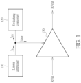
- FIG. 1 is a diagram illustrating a supply modulator and a power amplifier 130 according to one embodiment of the present invention, wherein the supply voltage comprises a linear amplifier 110 and a switching converter 120.
- the power amplifier 130 is configured to receive a radio frequency input signal RFin to generate a radio frequency output signal RFout, and a supply voltage of the power amplifier 130 is generated by the linear amplifier 110 and the switching converter 120.
- the switching converter 120 is configured to provide low-frequency current I SW with high efficiency
- the linear amplifier configured to provide high-frequency current I L with middle efficiency, and a summation of the current I SW and the current I L form an output current lout flowing into the power amplifier 130.
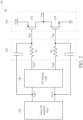
- FIG. 2 is a diagram illustrating the linear amplifier 110 according to one embodiment of the present invention.
- the linear amplifier 110 comprises an amplifier stage (a class-AB amplifier stage 210 in this embodiment), a DC-shifting stage 220, a compensation network 230 and a power stage 240.
- the compensation network 230 comprises capacitors C1, C2 and resistors R1 and R2, and the power stage 240 comprises a P-type Metal-Oxide-Semiconductor (PMOS) 242 and an N-type Metal-Oxide-Semiconductor (NMOS) 244 connected between a supply voltage VDD and a ground voltage, wherein the capacitor C1 is coupled between a first output terminal of the class-AB amplifier stage 210 and a gate electrode of the PMOS 242, the capacitor C2 is coupled between a second output terminal of the class-AB amplifier stage 210 and a gate electrode of the NMOS 244, the resistor R1 is coupled between a first output terminal of the DC-shifting stage 220 and the gate electrode of the PMOS 242, and the resistor R2 is coupled between a second output terminal of the DC-shifting stage 220 and the gate electrode of the NMOS 244.
- PMOS Metal-Oxide-Semiconductor
- NMOS N-type Metal-Oxide-Semic
- the power stage 240 shown in FIG. 2 is for illustrative, not a limitation of the present invention.
- one or more transistors/components may be positioned between the PMOS 242 and the supply voltage, and/or one or more transistors/components may be positioned between the PMOS 242 and the NMOS 244, and/or one or more transistors/components may be positioned between the NMOS 244 and the ground voltage.
- the class-AB amplifier stage 210 In the operation of the linear amplifier 110, the class-AB amplifier stage 210 generates a first signal Vgp1 and a second signal Vgn1, wherein each of the first signal Vgp1 and the second signal Vgn1 has a DC part (DC voltage) and an AC part (AC signal). Then, the DC-shifting stage 220 adjusts a DC voltage of the first signal Vgp1 to generate an adjusted first signal Vgp1', wherein a DC voltage of the adjusted first signal Vgp1' is different from the DC voltage of the first signal Vgp1, and in this embodiment, the DC voltage of the adjusted first signal Vgp1' is higher than the DC voltage of the first signal Vgp1.
- the DC-shifting stage 220 further adjusts the DC voltage of the second signal Vgn1 to generate an adjusted second signal Vgn1', wherein a DC voltage of the adjusted second signal Vgn1' is different from the DC voltage of the second signal Vgn1, and in this embodiment, the DC voltage of the adjusted second signal Vgn1' is lower than the DC voltage of the second signal Vgn1.
- the compensation network 230 receives the first signal Vgp1 and the adjusted first signal Vgp1' to generate a first driving signal Vgp, wherein a DC voltage of the first driving signal Vgp is from the adjusted first signal Vgp1' , and an AC signal of the adjusted first signal Vgp1' is from the first signal Vgp1.
- the resistor R1 and the capacitor C1 form a low-pass filter so that signal components below a -3dB corner frequency of the resistor R1 and the capacitor C1 passes through the resistor R1; and for the first signal Vgp1, the capacitor C1 and the resistor R1 form a high-pass filter so that the signal components above the -3dB corner frequency of the resistor R1 and the capacitor C1 passes through the capacitor C1; and the first driving signal Vgp is generated by combining a high-pass filtering result of the first signal Vgp1 and a low-pass filtering result of the adjusted first signal Vgp1'.
- the compensation network 230 receives the second signal Vgn1 and the adjusted second signal Vgn1' to generate a second driving signal Vgn, wherein a DC voltage of the second driving signal Vgn is from the adjusted second signal Vgn1', and an AC signal of the adjusted second signal Vgn1' is from the second signal Vgn1.
- the resistor R2 and the capacitor C2 form a low-pass filter so that signal components below a -3dB corner frequency of the resistor R2 and the capacitor C2 passes through the resistor R2; and for the second signal Vgn1, the capacitor C2 and the resistor R2 form a high-pass filter so that the signal components above the -3dB corner frequency of the resistor R2 and the capacitor C2 passes through the capacitor C2; and the second driving signal Vgn is generated by combining a high-pass filtering result of the second signal Vgn1 and a low-pass filtering result of the adjusted second signal Vgn1'.
- the PMOS 242 and the NMOS 244 of the power stage 240 receives the first driving signal Vgp and the second driving signal Vgn, respectively, to generate an output signal Vout.
- the detailed circuits within the compensation network 230 are for illustrative, not a limitation of the present invention. As long as the compensation network 230 performs a high-pass filtering operation on the first signal Vgp1, performs a low-pass filtering operation on the adjusted first signal Vgp1', and combines a high-pass filtering result of the first signal Vgp1 and a low-pass filtering result of the adjusted first signal Vgp1' to generate the first driving signal Vgp; and/or compensation network 230 performs a high-pass filtering operation on the second signal Vgn1, performs a low-pass filtering operation on the adjusted second signal Vgn1' , and combines a high-pass filtering result of the second signal Vgn1 and a low-pass filtering result of the adjusted second signal Vgn1' to generate the second driving signal Vgn, the compensation network 230 can have different circuit design.
- the first driving signal Vgp or the second driving signal Vgn can have appropriate DC voltage with enough AC swing.
- the first driving signal Vgp has a higher DC voltage and/or the second driving signal Vgn has a lower DC voltage
- the PMOS 242 and/or the NMOS 244 will have the smaller gate-source voltage (Vgs) so that the power stage 240 has smaller quiescent current.
- the linearity of the class-AB amplifier stage can have good linearity, and the swings of the first signal Vgp1 and the second signal Vgn1 are not worsened.
- FIG. 3 is a diagram illustrating the DC-shifting stage 220 according to one embodiment of the present invention.
- the DC-shifting stage 220 is implemented by using source followers.
- the DC-shifting stage 220 comprises a current source 302, a P-type transistor M1, an N-type transistor M2 and a current source 304, wherein the current source 302 is coupled between a supply voltage and a source electrode of the P-type transistor M1, a drain electrode of the P-type transistor M1 is coupled to a bias voltage Vbp, a drain electrode of the N-type transistor M2 is coupled to a bias voltage Vbn, and the current source 304 is coupled between the ground voltage and a source electrode of the N-type transistor M2.
- the P-type transistor M1 serves as a source follower to receive the first signal Vgp1 at the gate electrode to generate the adjusted first signal Vgp1'
- the N-type transistor M2 serves as a source follower to receive the second signal Vgn1 at the gate electrode to generate the adjusted second signal Vgn1'.
- FIG. 4 is a diagram illustrating the DC-shifting stage 220 according to one embodiment of the present invention.
- the DC-shifting stage 220 is implemented by using common source amplifiers.
- the DC-shifting stage 220 comprises a first common source amplifier and a second common source amplifier, wherein the first common source amplifier is implemented by using transistors M3 - M6, and the second common source amplifier is implemented by using transistors M7 - M10.
- the first common source amplifier receives the first signal Vgp1 at a gate electrode of the transistor M3 to generate the adjusted first signal Vgp1' at a drain electrode of the transistor M4, and the second common source amplifier receives the second signal Vgn1 at a gate electrode of the transistor M9 to generate the adjusted second signal Vgn1' at a drain electrode of the transistor M10.
- the DC-shifting stage 220 shown in FIG. 3 and FIG. 4 is for illustrative, not a limitation of the present invention. As long as the DC-shifting stage 220 can adjust the voltage levels of the first signal Vgp1 and the second signal Vgn1 to generate the adjusted first signal Vgp1' and the adjusted second signal Vgn1', respectively, the DC-shifting stage 220 can have any suitable design.
- the linear amplifier of the present invention by using the DC-shifting stage to de-couple the power stage and the amplifier stage, and using the compensation network to apply AC-coupled feedforward to preserve the AC signal, the first driving signal or the second driving signal inputted into the power stage can have appropriate DC voltage with enough AC swing. Therefore, the linear amplifier can have good linearity with low quiescent current.
Landscapes
- Engineering & Computer Science (AREA)
- Power Engineering (AREA)
- Microelectronics & Electronic Packaging (AREA)
- Amplifiers (AREA)
Abstract
Description
- This application claims the benefit of
U.S. Provisional Application No. 63/243, 765, filed on September 14th, 2021 - In a conventional linear amplifier used in a power modulator, an amplifier output stage within the linear amplifier is directly coupled to a power stage for generating a supply voltage. In the design of the power stage, a quiescent current is determined based on a gate-source voltage (Vgs) of the transistor within the power stage, that is, the power stage has lower quiescent current if the transistors have small gate-source voltages, and the power stage has larger quiescent current if the transistors have large gate-source voltages. However, because the transistors of the power stage receive output signals of the amplifier stage, if the transistors of the power transistor stage are designed to have small gate-source voltages to lower the quiescent current, the linearity of the amplifier stage will be worsened and the swings of output signals become smaller. Therefore, the linear amplifier has a trade-off between the quiescent current of the power stage and the linearity of the amplifier stage.
- It is therefore an objective of the present invention to provide a linear amplifier using a DC-shifting stage to de-couple the amplifier stage, to solve the above-mentioned problems.
- According to one embodiment of the present invention, a linear amplifier comprising an amplifier stage, a DC-shifting stage, a compensation network and a power stage. The amplifier stage is configured to generate a first signal and a second signal. The DC-shifting stage is configured to adjust a DC voltage of the first signal and a DC voltage of the second signal to generate an adjusted first signal and an adjusted second signal. The compensation network is configured to generate a first driving signal and a second driving signal according to the first signal, the second signal, the adjusted first signal and the adjusted second signal. The power stage is configured to generate an output signal according to the first driving signal and the second driving signal.
- These and other objectives of the present invention will no doubt become obvious to those of ordinary skill in the art after reading the following detailed description of the preferred embodiment that is illustrated in the various figures and drawings.
-
-
FIG. 1 is a diagram illustrating a supply modulator and a power amplifier according to one embodiment of the present invention. -
FIG. 2 is a diagram illustrating the linear amplifier according to one embodiment of the present invention. -
FIG. 3 is a diagram illustrating the DC-shifting stage according to one embodiment of the present invention. -
FIG. 4 is a diagram illustrating the DC-shifting stage according to one embodiment of the present invention. - Certain terms are used throughout the following description and claims to refer to particular system components. As one skilled in the art will appreciate, manufacturers may refer to a component by different names. This document does not intend to distinguish between components that differ in name but not function. In the following discussion and in the claims, the terms "including" and "comprising" are used in an open-ended fashion, and thus should be interpreted to mean "including, but not limited to ...". The terms "couple" and "couples" are intended to mean either an indirect or a direct electrical connection. Thus, if a first device couples to a second device, that connection may be through a direct electrical connection, or through an indirect electrical connection via other devices and connections.
-
FIG. 1 is a diagram illustrating a supply modulator and apower amplifier 130 according to one embodiment of the present invention, wherein the supply voltage comprises alinear amplifier 110 and aswitching converter 120. As shown inFIG. 1 , thepower amplifier 130 is configured to receive a radio frequency input signal RFin to generate a radio frequency output signal RFout, and a supply voltage of thepower amplifier 130 is generated by thelinear amplifier 110 and theswitching converter 120. Specifically, theswitching converter 120 is configured to provide low-frequency current ISW with high efficiency, and the linear amplifier configured to provide high-frequency current IL with middle efficiency, and a summation of the current ISW and the current IL form an output current lout flowing into thepower amplifier 130. -
FIG. 2 is a diagram illustrating thelinear amplifier 110 according to one embodiment of the present invention. As shown inFIG. 2 , thelinear amplifier 110 comprises an amplifier stage (a class-AB amplifier stage 210 in this embodiment), a DC-shiftingstage 220, acompensation network 230 and apower stage 240. Thecompensation network 230 comprises capacitors C1, C2 and resistors R1 and R2, and thepower stage 240 comprises a P-type Metal-Oxide-Semiconductor (PMOS) 242 and an N-type Metal-Oxide-Semiconductor (NMOS) 244 connected between a supply voltage VDD and a ground voltage, wherein the capacitor C1 is coupled between a first output terminal of the class-AB amplifier stage 210 and a gate electrode of thePMOS 242, the capacitor C2 is coupled between a second output terminal of the class-AB amplifier stage 210 and a gate electrode of theNMOS 244, the resistor R1 is coupled between a first output terminal of the DC-shifting stage 220 and the gate electrode of thePMOS 242, and the resistor R2 is coupled between a second output terminal of the DC-shiftingstage 220 and the gate electrode of theNMOS 244. - It is noted that the
power stage 240 shown inFIG. 2 is for illustrative, not a limitation of the present invention. In other embodiments, one or more transistors/components may be positioned between thePMOS 242 and the supply voltage, and/or one or more transistors/components may be positioned between thePMOS 242 and theNMOS 244, and/or one or more transistors/components may be positioned between theNMOS 244 and the ground voltage. - In the operation of the
linear amplifier 110, the class-AB amplifier stage 210 generates a first signal Vgp1 and a second signal Vgn1, wherein each of the first signal Vgp1 and the second signal Vgn1 has a DC part (DC voltage) and an AC part (AC signal). Then, the DC-shifting stage 220 adjusts a DC voltage of the first signal Vgp1 to generate an adjusted first signal Vgp1', wherein a DC voltage of the adjusted first signal Vgp1' is different from the DC voltage of the first signal Vgp1, and in this embodiment, the DC voltage of the adjusted first signal Vgp1' is higher than the DC voltage of the first signal Vgp1. The DC-shifting stage 220 further adjusts the DC voltage of the second signal Vgn1 to generate an adjusted second signal Vgn1', wherein a DC voltage of the adjusted second signal Vgn1' is different from the DC voltage of the second signal Vgn1, and in this embodiment, the DC voltage of the adjusted second signal Vgn1' is lower than the DC voltage of the second signal Vgn1. - Then, the
compensation network 230 receives the first signal Vgp1 and the adjusted first signal Vgp1' to generate a first driving signal Vgp, wherein a DC voltage of the first driving signal Vgp is from the adjusted first signal Vgp1' , and an AC signal of the adjusted first signal Vgp1' is from the first signal Vgp1. Specifically, for the adjusted first signal Vgp1', the resistor R1 and the capacitor C1 form a low-pass filter so that signal components below a -3dB corner frequency of the resistor R1 and the capacitor C1 passes through the resistor R1; and for the first signal Vgp1, the capacitor C1 and the resistor R1 form a high-pass filter so that the signal components above the -3dB corner frequency of the resistor R1 and the capacitor C1 passes through the capacitor C1; and the first driving signal Vgp is generated by combining a high-pass filtering result of the first signal Vgp1 and a low-pass filtering result of the adjusted first signal Vgp1'. Similarly, thecompensation network 230 receives the second signal Vgn1 and the adjusted second signal Vgn1' to generate a second driving signal Vgn, wherein a DC voltage of the second driving signal Vgn is from the adjusted second signal Vgn1', and an AC signal of the adjusted second signal Vgn1' is from the second signal Vgn1. Specifically, for the adjusted second signal Vgn1', the resistor R2 and the capacitor C2 form a low-pass filter so that signal components below a -3dB corner frequency of the resistor R2 and the capacitor C2 passes through the resistor R2; and for the second signal Vgn1, the capacitor C2 and the resistor R2 form a high-pass filter so that the signal components above the -3dB corner frequency of the resistor R2 and the capacitor C2 passes through the capacitor C2; and the second driving signal Vgn is generated by combining a high-pass filtering result of the second signal Vgn1 and a low-pass filtering result of the adjusted second signal Vgn1'. - Then, the PMOS 242 and the NMOS 244 of the
power stage 240 receives the first driving signal Vgp and the second driving signal Vgn, respectively, to generate an output signal Vout. - It is noted that the detailed circuits within the
compensation network 230 are for illustrative, not a limitation of the present invention. As long as thecompensation network 230 performs a high-pass filtering operation on the first signal Vgp1, performs a low-pass filtering operation on the adjusted first signal Vgp1', and combines a high-pass filtering result of the first signal Vgp1 and a low-pass filtering result of the adjusted first signal Vgp1' to generate the first driving signal Vgp; and/orcompensation network 230 performs a high-pass filtering operation on the second signal Vgn1, performs a low-pass filtering operation on the adjusted second signal Vgn1' , and combines a high-pass filtering result of the second signal Vgn1 and a low-pass filtering result of the adjusted second signal Vgn1' to generate the second driving signal Vgn, thecompensation network 230 can have different circuit design. - In the above embodiment, by using the DC-shifting stage to de-couple the power stage and the class-AB amplifier stage, and using feedforward paths (i.e., R1/C1/R2/C2 in the compensation network 230) to apply AC-coupled feedforward to preserve the AC signal (i.e., class-AB signal), the first driving signal Vgp or the second driving signal Vgn can have appropriate DC voltage with enough AC swing. Specifically, in this embodiment, because the first driving signal Vgp has a higher DC voltage and/or the second driving signal Vgn has a lower DC voltage, the
PMOS 242 and/or theNMOS 244 will have the smaller gate-source voltage (Vgs) so that thepower stage 240 has smaller quiescent current. In addition, because the DC voltage the first signal Vgp1 can be lower than the DC voltage the adjusted first signal Vgp1', and/or the DC voltage the second signal Vgn1 can be higher than the DC voltage the adjusted second signal Vgn1', the linearity of the class-AB amplifier stage can have good linearity, and the swings of the first signal Vgp1 and the second signal Vgn1 are not worsened. -
FIG. 3 is a diagram illustrating the DC-shiftingstage 220 according to one embodiment of the present invention. As shown inFIG. 3 , the DC-shiftingstage 220 is implemented by using source followers. Specifically, the DC-shiftingstage 220 comprises acurrent source 302, a P-type transistor M1, an N-type transistor M2 and acurrent source 304, wherein thecurrent source 302 is coupled between a supply voltage and a source electrode of the P-type transistor M1, a drain electrode of the P-type transistor M1 is coupled to a bias voltage Vbp, a drain electrode of the N-type transistor M2 is coupled to a bias voltage Vbn, and thecurrent source 304 is coupled between the ground voltage and a source electrode of the N-type transistor M2. In the operation of the DC-shiftingstage 220, the P-type transistor M1 serves as a source follower to receive the first signal Vgp1 at the gate electrode to generate the adjusted first signal Vgp1', and the N-type transistor M2 serves as a source follower to receive the second signal Vgn1 at the gate electrode to generate the adjusted second signal Vgn1'. -
FIG. 4 is a diagram illustrating the DC-shiftingstage 220 according to one embodiment of the present invention. As shown inFIG. 4 , the DC-shiftingstage 220 is implemented by using common source amplifiers. Specifically, the DC-shiftingstage 220 comprises a first common source amplifier and a second common source amplifier, wherein the first common source amplifier is implemented by using transistors M3 - M6, and the second common source amplifier is implemented by using transistors M7 - M10. In the operation of the DC-shifting stage, the first common source amplifier receives the first signal Vgp1 at a gate electrode of the transistor M3 to generate the adjusted first signal Vgp1' at a drain electrode of the transistor M4, and the second common source amplifier receives the second signal Vgn1 at a gate electrode of the transistor M9 to generate the adjusted second signal Vgn1' at a drain electrode of the transistor M10. - It is noted that the DC-shifting
stage 220 shown inFIG. 3 andFIG. 4 is for illustrative, not a limitation of the present invention. As long as the DC-shiftingstage 220 can adjust the voltage levels of the first signal Vgp1 and the second signal Vgn1 to generate the adjusted first signal Vgp1' and the adjusted second signal Vgn1', respectively, the DC-shiftingstage 220 can have any suitable design. - Briefly summarized, in the linear amplifier of the present invention, by using the DC-shifting stage to de-couple the power stage and the amplifier stage, and using the compensation network to apply AC-coupled feedforward to preserve the AC signal, the first driving signal or the second driving signal inputted into the power stage can have appropriate DC voltage with enough AC swing. Therefore, the linear amplifier can have good linearity with low quiescent current.
- Those skilled in the art will readily observe that numerous modifications and alterations of the device and method may be made while retaining the teachings of the invention. Accordingly, the above disclosure should be construed as limited only by the metes and bounds of the appended claims.
Claims (11)
- A linear amplifier (110), comprising:an amplifier stage, configured to generate a first signal (Vgp1) and a second signal (Vgn1);a DC-shifting stage (220), configured to adjust a DC voltage of the first signal (Vgp1) and a DC voltage of the second signal (Vgn1) to generate an adjusted first signal (Vgp1') and an adjusted second signal (Vgn1');a compensation network (230), configured to generate a first driving signal (Vgp) and a second driving signal (Vgn) according to the first signal (Vgp1), the second signal (Vgn1), the adjusted first signal (Vgp1') and the adjusted second signal (Vgn1'); anda power stage (240), configured to generate an output signal according to the first driving signal (Vgp) and the second driving signal (Vgn).
- The linear amplifier (110) of claim 1, wherein a DC voltage of the adjusted first signal (Vgp1' ) is different from the DC voltage of the first signal (Vgp1), and a DC voltage of the adjusted second signal (Vgn1') is different from the DC voltage of the second signal (Vgn1).
- The linear amplifier (110) of claim 2, wherein the DC voltage of the adjusted first signal (Vgp1') is higher than the DC voltage of the first signal (Vgp1), and the DC voltage of the adjusted second signal (Vgn1') is lower than the DC voltage of the second signal (Vgn1).
- The linear amplifier (110) of claim 3, wherein the compensation network (230) generates the first driving signal (Vgp) according to the first signal (Vgp1) and the adjusted first signal (Vgp1'), and generates the second driving signal (Vgn) according to the second signal (Vgn1) and the adjusted second signal (Vgn1'); the power stage (240) comprises a P-type transistor (M1) and an N-type transistor (M2) connected in series, and a gate electrode of the P-type transistor (M1) receives the first driving signal (Vgp) and a gate electrode of the N-type transistor (M2) receives the second driving signal (Vgn) to generate the output signal.
- The linear amplifier (110) of claim 1, wherein the compensation network (230) comprises a first feedforward path to preserve an AC component of the first signal (Vgp1) in the first driving signal (Vgp), and the compensation network (230) comprises a second feedforward path to preserve an AC component of the second signal (Vgn1) in the second driving signal(Vgn).
- The linear amplifier (110) of claim 1, wherein the compensation network (230) performs a high-pass filtering operation on the first signal (Vgp1), performs a low-pass filtering operation on the adjusted first signal (Vgp1'), and combines a high-pass filtering result of the first signal (Vgp1) and a low-pass filtering result of the adjusted first signal (Vgp1') to generate the first driving signal (Vgp).
- The linear amplifier (110) of claim 1, wherein the compensation network (230) performs a high-pass filtering operation on the second signal (Vgn1), performs a low-pass filtering operation on the adjusted second signal (Vgn1'), and combines a high-pass filtering result of the second signal (Vgn1) and a low-pass filtering result of the adjusted second signal (Vgn1') to generate the second driving signal(Vgn).
- The linear amplifier (110) of claim 1, wherein the compensation network (230) comprises a first capacitor (C1) and a first resistor (R1), a first node of the first capacitor (C1) is used to receive the first signal (Vgp1), a first node of the first resistor (R1) is used to receive the adjusted first signal (Vgp1'), and a second node of the first capacitor (C1) is coupled to a second node of the first resistor (R1) ; and the first driving signal (Vgp) is generated at the second node of the first capacitor (C1) or the second node of the first resistor (R1).
- The linear amplifier (110) of claim 1, wherein the compensation network (230) comprises a second capacitor (C2) and a second resistor (R2), a first node of the second capacitor (C2) is used to receive the second signal (Vgn1), a first node of the second resistor (R2) is used to receive the adjusted second signal (Vgn1'), and a second node of the second capacitor (C2) is coupled to a second node of the second resistor (R2) ; and the second driving signal (Vgn) is generated at the second node of the second capacitor (C2) or the second node of the second resistor (R2).
- The linear amplifier (110) of claim 1, wherein the amplifier stage is a class-AB amplifier stage (210).
- The linear amplifier (110) of claim 1, wherein the linear amplifier (110) is used in a supply modulator.
Priority Applications (1)
| Application Number | Priority Date | Filing Date | Title |
|---|---|---|---|
| EP25204447.4A EP4645692A3 (en) | 2021-09-14 | 2022-08-18 | Amplifier output stage with dc-shifting circuit for high-speed supply modulator |
Applications Claiming Priority (2)
| Application Number | Priority Date | Filing Date | Title |
|---|---|---|---|
| US202163243765P | 2021-09-14 | 2021-09-14 | |
| US17/884,589 US12407305B2 (en) | 2021-09-14 | 2022-08-10 | Amplifier output stage with DC-shifting circuit for high-speed supply modulator |
Related Child Applications (2)
| Application Number | Title | Priority Date | Filing Date |
|---|---|---|---|
| EP25204447.4A Division-Into EP4645692A3 (en) | 2021-09-14 | 2022-08-18 | Amplifier output stage with dc-shifting circuit for high-speed supply modulator |
| EP25204447.4A Division EP4645692A3 (en) | 2021-09-14 | 2022-08-18 | Amplifier output stage with dc-shifting circuit for high-speed supply modulator |
Publications (2)
| Publication Number | Publication Date |
|---|---|
| EP4148992A1 true EP4148992A1 (en) | 2023-03-15 |
| EP4148992B1 EP4148992B1 (en) | 2025-12-24 |
Family
ID=82942535
Family Applications (2)
| Application Number | Title | Priority Date | Filing Date |
|---|---|---|---|
| EP25204447.4A Pending EP4645692A3 (en) | 2021-09-14 | 2022-08-18 | Amplifier output stage with dc-shifting circuit for high-speed supply modulator |
| EP22190915.3A Active EP4148992B1 (en) | 2021-09-14 | 2022-08-18 | Amplifier output stage with dc-shifting circuit for high-speed supply modulator |
Family Applications Before (1)
| Application Number | Title | Priority Date | Filing Date |
|---|---|---|---|
| EP25204447.4A Pending EP4645692A3 (en) | 2021-09-14 | 2022-08-18 | Amplifier output stage with dc-shifting circuit for high-speed supply modulator |
Country Status (4)
| Country | Link |
|---|---|
| US (1) | US12407305B2 (en) |
| EP (2) | EP4645692A3 (en) |
| CN (1) | CN115811281A (en) |
| TW (1) | TWI833350B (en) |
Citations (4)
| Publication number | Priority date | Publication date | Assignee | Title |
|---|---|---|---|---|
| US4864249A (en) * | 1988-02-29 | 1989-09-05 | Reiffin Martin G | Nonslewing amplifier |
| US8008975B1 (en) * | 2009-03-31 | 2011-08-30 | Cirrus Logic, Inc. | Gate-boosted, variable voltage supply rail amplifier |
| CN110311636A (en) * | 2019-06-29 | 2019-10-08 | 复旦大学 | High Bandwidth and High Swing Linear Amplifier for Envelope Tracking Power Supply Modulator |
| EP3367564B1 (en) * | 2017-02-23 | 2021-03-31 | MediaTek Inc. | Linear amplifier having higher efficiency for envelope tracking modulator |
Family Cites Families (12)
| Publication number | Priority date | Publication date | Assignee | Title |
|---|---|---|---|---|
| US5512859A (en) * | 1994-11-16 | 1996-04-30 | National Semiconductor Corporation | Amplifier stage having compensation for NPN, PNP beta mismatch and improved slew rate |
| US7161422B2 (en) | 2003-01-03 | 2007-01-09 | Junghyun Kim | Multiple power mode amplifier with bias modulation option and without bypass switches |
| US7378903B2 (en) * | 2004-06-07 | 2008-05-27 | Sonos, Inc. | System and method for minimizing DC offset in outputs of audio power amplifiers |
| US8427235B2 (en) | 2007-04-13 | 2013-04-23 | Advanced Analogic Technologies, Inc. | Power-MOSFETs with improved efficiency for multi-channel class-D audio amplifiers and packaging thereof |
| CN101471633B (en) * | 2007-12-29 | 2013-01-30 | 瑞昱半导体股份有限公司 | Output stage bias circuit and operational amplifier using the same |
| CN101339443B (en) * | 2008-08-08 | 2011-02-16 | 武汉大学 | Broad output current scope low pressure difference linear manostat |
| CN102449903B (en) | 2009-02-25 | 2016-03-09 | Thx有限公司 | Low dissipation amplifier |
| US10289140B2 (en) | 2016-10-27 | 2019-05-14 | Stmicroelectronics Design And Application S.R.O. | Voltage regulator having bias current boosting |
| US10574193B2 (en) * | 2017-01-25 | 2020-02-25 | Mediatek Inc. | Class AB amplifier having cascode stage with filter for improving linearity |
| EP3425795B1 (en) | 2017-07-03 | 2021-09-01 | Infineon Technologies Austria AG | Class d audio amplifier with overload protection circuit |
| KR102069634B1 (en) * | 2018-07-05 | 2020-01-23 | 삼성전기주식회사 | Multi stage power amplifier having linearity compensating function |
| US11099589B1 (en) | 2020-03-16 | 2021-08-24 | Alpha And Omega Semiconductor (Cayman) Ltd. | Digitally programmable, fully differential error amplifier |
-
2022
- 2022-08-10 US US17/884,589 patent/US12407305B2/en active Active
- 2022-08-18 EP EP25204447.4A patent/EP4645692A3/en active Pending
- 2022-08-18 EP EP22190915.3A patent/EP4148992B1/en active Active
- 2022-08-19 CN CN202211001303.6A patent/CN115811281A/en active Pending
- 2022-09-13 TW TW111134447A patent/TWI833350B/en active
Patent Citations (4)
| Publication number | Priority date | Publication date | Assignee | Title |
|---|---|---|---|---|
| US4864249A (en) * | 1988-02-29 | 1989-09-05 | Reiffin Martin G | Nonslewing amplifier |
| US8008975B1 (en) * | 2009-03-31 | 2011-08-30 | Cirrus Logic, Inc. | Gate-boosted, variable voltage supply rail amplifier |
| EP3367564B1 (en) * | 2017-02-23 | 2021-03-31 | MediaTek Inc. | Linear amplifier having higher efficiency for envelope tracking modulator |
| CN110311636A (en) * | 2019-06-29 | 2019-10-08 | 复旦大学 | High Bandwidth and High Swing Linear Amplifier for Envelope Tracking Power Supply Modulator |
Non-Patent Citations (2)
| Title |
|---|
| BRITTON JR C L ET AL: "A FOUR-CHANNEL BIPOLAR MONOLITHIC PREAMPLIFIER FOR RHIC DIMUON PAD READOUT", PROCEEDINGS OF THE NUCLEAR SCIENCE SYMPOSIUM AND MEDICAL IMAGING CONFERENCE. SANTA FE, NOV. 2 - 9, 1991; [PROCEEDINGS OF THE NUCLEAR SCIENCE SYMPOSIUM AND MEDICAL IMAGING CONFERENCE], NEW YORK, IEEE, US, vol. 1 OF 03, 2 November 1991 (1991-11-02), pages 639 - 643, XP000347920, ISBN: 978-0-7803-0513-7, DOI: 10.1109/NSSMIC.1991.259016 * |
| MAHMOUDIDARYAN PARISA ET AL: "Wideband Hybrid Envelope Tracking Modulator With Hysteretic-Controlled Three-Level Switching Converter and Slew-Rate Enhanced Linear Amplifier", IEEE JOURNAL OF SOLID-STATE CIRCUITS, IEEE, USA, vol. 54, no. 12, 2 December 2019 (2019-12-02), pages 3336 - 3347, XP011752832, ISSN: 0018-9200, [retrieved on 20191121], DOI: 10.1109/JSSC.2019.2941014 * |
Also Published As
| Publication number | Publication date |
|---|---|
| CN115811281A (en) | 2023-03-17 |
| TWI833350B (en) | 2024-02-21 |
| TW202312657A (en) | 2023-03-16 |
| US20230078955A1 (en) | 2023-03-16 |
| US12407305B2 (en) | 2025-09-02 |
| EP4148992B1 (en) | 2025-12-24 |
| EP4645692A2 (en) | 2025-11-05 |
| EP4645692A3 (en) | 2025-12-03 |
Similar Documents
| Publication | Publication Date | Title |
|---|---|---|
| US8149055B2 (en) | Semiconductor integrated circuit device | |
| US5177450A (en) | Cmos power amplifier | |
| US8067958B2 (en) | Mitigating side effects of impedance transformation circuits | |
| US8294518B2 (en) | Class-AB/B amplifier and quiescent control circuit for implementation with same | |
| US7948294B2 (en) | Mixer with high linearity | |
| US7271663B2 (en) | Operational amplifier output stage and method | |
| US11664774B2 (en) | Operational amplifier using single-stage amplifier with slew-rate enhancement and associated method | |
| US6833760B1 (en) | Low power differential amplifier powered by multiple unequal power supply voltages | |
| US20040108897A1 (en) | Audio amplifier | |
| US10566933B2 (en) | Low voltage amplifier with gain boost circuit | |
| US12407305B2 (en) | Amplifier output stage with DC-shifting circuit for high-speed supply modulator | |
| US12388420B2 (en) | Noise filter circuit with controllable transistor off-resistance and associated noise filtering method | |
| US7193468B2 (en) | Active load circuit for low-voltage CMOS voltage gain amplifier with wide bandwidth and high gain characteristic | |
| US10574193B2 (en) | Class AB amplifier having cascode stage with filter for improving linearity | |
| US20170324387A1 (en) | Input feed-forward technique for class ab amplifier | |
| JP2010273284A (en) | High frequency amplifier | |
| GB2593279A (en) | Dual bootstrapping for an open-loop pulse width modulation driver | |
| US12395136B2 (en) | High-efficiency amplifier architecture with de-gain stage | |
| EP4312366A1 (en) | Circuit with a pseudo class-ab structure | |
| US20260066896A1 (en) | Source follower circuit with feedback loop and self-biased diode-connected metal-oxide-semiconductor load | |
| US11190168B2 (en) | Dual bootstrapping for an open-loop pulse width modulation driver | |
| CN108259012B (en) | Power amplifier of broadband power line |
Legal Events
| Date | Code | Title | Description |
|---|---|---|---|
| PUAI | Public reference made under article 153(3) epc to a published international application that has entered the european phase |
Free format text: ORIGINAL CODE: 0009012 |
|
| STAA | Information on the status of an ep patent application or granted ep patent |
Free format text: STATUS: THE APPLICATION HAS BEEN PUBLISHED |
|
| AK | Designated contracting states |
Kind code of ref document: A1 Designated state(s): AL AT BE BG CH CY CZ DE DK EE ES FI FR GB GR HR HU IE IS IT LI LT LU LV MC MK MT NL NO PL PT RO RS SE SI SK SM TR |
|
| P01 | Opt-out of the competence of the unified patent court (upc) registered |
Effective date: 20230607 |
|
| STAA | Information on the status of an ep patent application or granted ep patent |
Free format text: STATUS: REQUEST FOR EXAMINATION WAS MADE |
|
| 17P | Request for examination filed |
Effective date: 20230830 |
|
| RBV | Designated contracting states (corrected) |
Designated state(s): AL AT BE BG CH CY CZ DE DK EE ES FI FR GB GR HR HU IE IS IT LI LT LU LV MC MK MT NL NO PL PT RO RS SE SI SK SM TR |
|
| RIC1 | Information provided on ipc code assigned before grant |
Ipc: H03F 3/21 20060101AFI20250612BHEP Ipc: H03F 3/26 20060101ALI20250612BHEP Ipc: H03F 1/02 20060101ALI20250612BHEP Ipc: H03F 3/213 20060101ALI20250612BHEP Ipc: H03F 3/30 20060101ALI20250612BHEP Ipc: H03F 3/19 20060101ALI20250612BHEP |
|
| GRAP | Despatch of communication of intention to grant a patent |
Free format text: ORIGINAL CODE: EPIDOSNIGR1 |
|
| STAA | Information on the status of an ep patent application or granted ep patent |
Free format text: STATUS: GRANT OF PATENT IS INTENDED |
|
| INTG | Intention to grant announced |
Effective date: 20250718 |
|
| GRAS | Grant fee paid |
Free format text: ORIGINAL CODE: EPIDOSNIGR3 |
|
| GRAA | (expected) grant |
Free format text: ORIGINAL CODE: 0009210 |
|
| STAA | Information on the status of an ep patent application or granted ep patent |
Free format text: STATUS: THE PATENT HAS BEEN GRANTED |
|
| AK | Designated contracting states |
Kind code of ref document: B1 Designated state(s): AL AT BE BG CH CY CZ DE DK EE ES FI FR GB GR HR HU IE IS IT LI LT LU LV MC MK MT NL NO PL PT RO RS SE SI SK SM TR |
|
| REG | Reference to a national code |
Ref country code: CH Ref legal event code: F10 Free format text: ST27 STATUS EVENT CODE: U-0-0-F10-F00 (AS PROVIDED BY THE NATIONAL OFFICE) Effective date: 20251224 Ref country code: GB Ref legal event code: FG4D |
|
| REG | Reference to a national code |
Ref country code: DE Ref legal event code: R096 Ref document number: 602022027310 Country of ref document: DE |
|
| REG | Reference to a national code |
Ref country code: LT Ref legal event code: MG9D |
|
| PG25 | Lapsed in a contracting state [announced via postgrant information from national office to epo] |
Ref country code: NO Free format text: LAPSE BECAUSE OF FAILURE TO SUBMIT A TRANSLATION OF THE DESCRIPTION OR TO PAY THE FEE WITHIN THE PRESCRIBED TIME-LIMIT Effective date: 20260324 |
|
| PG25 | Lapsed in a contracting state [announced via postgrant information from national office to epo] |
Ref country code: FI Free format text: LAPSE BECAUSE OF FAILURE TO SUBMIT A TRANSLATION OF THE DESCRIPTION OR TO PAY THE FEE WITHIN THE PRESCRIBED TIME-LIMIT Effective date: 20251224 Ref country code: HR Free format text: LAPSE BECAUSE OF FAILURE TO SUBMIT A TRANSLATION OF THE DESCRIPTION OR TO PAY THE FEE WITHIN THE PRESCRIBED TIME-LIMIT Effective date: 20251224 |
|
| PG25 | Lapsed in a contracting state [announced via postgrant information from national office to epo] |
Ref country code: RS Free format text: LAPSE BECAUSE OF FAILURE TO SUBMIT A TRANSLATION OF THE DESCRIPTION OR TO PAY THE FEE WITHIN THE PRESCRIBED TIME-LIMIT Effective date: 20260324 |
|
| PG25 | Lapsed in a contracting state [announced via postgrant information from national office to epo] |
Ref country code: LV Free format text: LAPSE BECAUSE OF FAILURE TO SUBMIT A TRANSLATION OF THE DESCRIPTION OR TO PAY THE FEE WITHIN THE PRESCRIBED TIME-LIMIT Effective date: 20251224 |
|
| REG | Reference to a national code |
Ref country code: NL Ref legal event code: MP Effective date: 20251224 |
|
| PG25 | Lapsed in a contracting state [announced via postgrant information from national office to epo] |
Ref country code: BG Free format text: LAPSE BECAUSE OF FAILURE TO SUBMIT A TRANSLATION OF THE DESCRIPTION OR TO PAY THE FEE WITHIN THE PRESCRIBED TIME-LIMIT Effective date: 20251224 |
|
| REG | Reference to a national code |
Ref country code: AT Ref legal event code: MK05 Ref document number: 1871753 Country of ref document: AT Kind code of ref document: T Effective date: 20251224 |
|
| PG25 | Lapsed in a contracting state [announced via postgrant information from national office to epo] |
Ref country code: NL Free format text: LAPSE BECAUSE OF FAILURE TO SUBMIT A TRANSLATION OF THE DESCRIPTION OR TO PAY THE FEE WITHIN THE PRESCRIBED TIME-LIMIT Effective date: 20251224 |
|
| PG25 | Lapsed in a contracting state [announced via postgrant information from national office to epo] |
Ref country code: LT Free format text: LAPSE BECAUSE OF FAILURE TO SUBMIT A TRANSLATION OF THE DESCRIPTION OR TO PAY THE FEE WITHIN THE PRESCRIBED TIME-LIMIT Effective date: 20251224 |
|
| PG25 | Lapsed in a contracting state [announced via postgrant information from national office to epo] |
Ref country code: SM Free format text: LAPSE BECAUSE OF FAILURE TO SUBMIT A TRANSLATION OF THE DESCRIPTION OR TO PAY THE FEE WITHIN THE PRESCRIBED TIME-LIMIT Effective date: 20251224 |
|
| PG25 | Lapsed in a contracting state [announced via postgrant information from national office to epo] |
Ref country code: ES Free format text: LAPSE BECAUSE OF FAILURE TO SUBMIT A TRANSLATION OF THE DESCRIPTION OR TO PAY THE FEE WITHIN THE PRESCRIBED TIME-LIMIT Effective date: 20251224 |
|
| PG25 | Lapsed in a contracting state [announced via postgrant information from national office to epo] |
Ref country code: PL Free format text: LAPSE BECAUSE OF FAILURE TO SUBMIT A TRANSLATION OF THE DESCRIPTION OR TO PAY THE FEE WITHIN THE PRESCRIBED TIME-LIMIT Effective date: 20251224 |
|
| PGFP | Annual fee paid to national office [announced via postgrant information from national office to epo] |
Ref country code: GB Payment date: 20260630 Year of fee payment: 5 |
|
| PG25 | Lapsed in a contracting state [announced via postgrant information from national office to epo] |
Ref country code: IT Free format text: LAPSE BECAUSE OF FAILURE TO SUBMIT A TRANSLATION OF THE DESCRIPTION OR TO PAY THE FEE WITHIN THE PRESCRIBED TIME-LIMIT Effective date: 20251224 |
|
| PG25 | Lapsed in a contracting state [announced via postgrant information from national office to epo] |
Ref country code: AT Free format text: LAPSE BECAUSE OF FAILURE TO SUBMIT A TRANSLATION OF THE DESCRIPTION OR TO PAY THE FEE WITHIN THE PRESCRIBED TIME-LIMIT Effective date: 20251224 |
|
| PG25 | Lapsed in a contracting state [announced via postgrant information from national office to epo] |
Ref country code: EE Free format text: LAPSE BECAUSE OF FAILURE TO SUBMIT A TRANSLATION OF THE DESCRIPTION OR TO PAY THE FEE WITHIN THE PRESCRIBED TIME-LIMIT Effective date: 20251224 |
|
| PG25 | Lapsed in a contracting state [announced via postgrant information from national office to epo] |
Ref country code: IS Free format text: LAPSE BECAUSE OF FAILURE TO SUBMIT A TRANSLATION OF THE DESCRIPTION OR TO PAY THE FEE WITHIN THE PRESCRIBED TIME-LIMIT Effective date: 20260424 Ref country code: PT Free format text: LAPSE BECAUSE OF FAILURE TO SUBMIT A TRANSLATION OF THE DESCRIPTION OR TO PAY THE FEE WITHIN THE PRESCRIBED TIME-LIMIT Effective date: 20260424 |
|
| PG25 | Lapsed in a contracting state [announced via postgrant information from national office to epo] |
Ref country code: CZ Free format text: LAPSE BECAUSE OF FAILURE TO SUBMIT A TRANSLATION OF THE DESCRIPTION OR TO PAY THE FEE WITHIN THE PRESCRIBED TIME-LIMIT Effective date: 20251224 |
|
| PGFP | Annual fee paid to national office [announced via postgrant information from national office to epo] |
Ref country code: FR Payment date: 20260608 Year of fee payment: 5 |
|
| PG25 | Lapsed in a contracting state [announced via postgrant information from national office to epo] |
Ref country code: SK Free format text: LAPSE BECAUSE OF FAILURE TO SUBMIT A TRANSLATION OF THE DESCRIPTION OR TO PAY THE FEE WITHIN THE PRESCRIBED TIME-LIMIT Effective date: 20251224 |
|
| PG25 | Lapsed in a contracting state [announced via postgrant information from national office to epo] |
Ref country code: SE Free format text: LAPSE BECAUSE OF FAILURE TO SUBMIT A TRANSLATION OF THE DESCRIPTION OR TO PAY THE FEE WITHIN THE PRESCRIBED TIME-LIMIT Effective date: 20251224 |