EP4148809A1 - Solar cell, method for preparing same and solar cell module - Google Patents
Solar cell, method for preparing same and solar cell module Download PDFInfo
- Publication number
- EP4148809A1 EP4148809A1 EP21202789.0A EP21202789A EP4148809A1 EP 4148809 A1 EP4148809 A1 EP 4148809A1 EP 21202789 A EP21202789 A EP 21202789A EP 4148809 A1 EP4148809 A1 EP 4148809A1
- Authority
- EP
- European Patent Office
- Prior art keywords
- passivation layer
- layer
- substrate
- range
- solar cell
- Prior art date
- Legal status (The legal status is an assumption and is not a legal conclusion. Google has not performed a legal analysis and makes no representation as to the accuracy of the status listed.)
- Granted
Links
Images




Classifications
-
- H—ELECTRICITY
- H10—SEMICONDUCTOR DEVICES; ELECTRIC SOLID-STATE DEVICES NOT OTHERWISE PROVIDED FOR
- H10F—INORGANIC SEMICONDUCTOR DEVICES SENSITIVE TO INFRARED RADIATION, LIGHT, ELECTROMAGNETIC RADIATION OF SHORTER WAVELENGTH OR CORPUSCULAR RADIATION
- H10F19/00—Integrated devices, or assemblies of multiple devices, comprising at least one photovoltaic cell covered by group H10F10/00, e.g. photovoltaic modules
- H10F19/80—Encapsulations or containers for integrated devices, or assemblies of multiple devices, having photovoltaic cells
-
- H—ELECTRICITY
- H10—SEMICONDUCTOR DEVICES; ELECTRIC SOLID-STATE DEVICES NOT OTHERWISE PROVIDED FOR
- H10F—INORGANIC SEMICONDUCTOR DEVICES SENSITIVE TO INFRARED RADIATION, LIGHT, ELECTROMAGNETIC RADIATION OF SHORTER WAVELENGTH OR CORPUSCULAR RADIATION
- H10F19/00—Integrated devices, or assemblies of multiple devices, comprising at least one photovoltaic cell covered by group H10F10/00, e.g. photovoltaic modules
- H10F19/90—Structures for connecting between photovoltaic cells, e.g. interconnections or insulating spacers
- H10F19/902—Structures for connecting between photovoltaic cells, e.g. interconnections or insulating spacers for series or parallel connection of photovoltaic cells
-
- H—ELECTRICITY
- H10—SEMICONDUCTOR DEVICES; ELECTRIC SOLID-STATE DEVICES NOT OTHERWISE PROVIDED FOR
- H10F—INORGANIC SEMICONDUCTOR DEVICES SENSITIVE TO INFRARED RADIATION, LIGHT, ELECTROMAGNETIC RADIATION OF SHORTER WAVELENGTH OR CORPUSCULAR RADIATION
- H10F71/00—Manufacture or treatment of devices covered by this subclass
- H10F71/128—Annealing
-
- H—ELECTRICITY
- H10—SEMICONDUCTOR DEVICES; ELECTRIC SOLID-STATE DEVICES NOT OTHERWISE PROVIDED FOR
- H10F—INORGANIC SEMICONDUCTOR DEVICES SENSITIVE TO INFRARED RADIATION, LIGHT, ELECTROMAGNETIC RADIATION OF SHORTER WAVELENGTH OR CORPUSCULAR RADIATION
- H10F71/00—Manufacture or treatment of devices covered by this subclass
- H10F71/129—Passivating
-
- H—ELECTRICITY
- H10—SEMICONDUCTOR DEVICES; ELECTRIC SOLID-STATE DEVICES NOT OTHERWISE PROVIDED FOR
- H10F—INORGANIC SEMICONDUCTOR DEVICES SENSITIVE TO INFRARED RADIATION, LIGHT, ELECTROMAGNETIC RADIATION OF SHORTER WAVELENGTH OR CORPUSCULAR RADIATION
- H10F77/00—Constructional details of devices covered by this subclass
- H10F77/30—Coatings
- H10F77/306—Coatings for devices having potential barriers
- H10F77/311—Coatings for devices having potential barriers for photovoltaic cells
-
- H—ELECTRICITY
- H10—SEMICONDUCTOR DEVICES; ELECTRIC SOLID-STATE DEVICES NOT OTHERWISE PROVIDED FOR
- H10F—INORGANIC SEMICONDUCTOR DEVICES SENSITIVE TO INFRARED RADIATION, LIGHT, ELECTROMAGNETIC RADIATION OF SHORTER WAVELENGTH OR CORPUSCULAR RADIATION
- H10F77/00—Constructional details of devices covered by this subclass
- H10F77/30—Coatings
- H10F77/306—Coatings for devices having potential barriers
- H10F77/311—Coatings for devices having potential barriers for photovoltaic cells
- H10F77/315—Coatings for devices having potential barriers for photovoltaic cells the coatings being antireflective or having enhancing optical properties
-
- H—ELECTRICITY
- H10—SEMICONDUCTOR DEVICES; ELECTRIC SOLID-STATE DEVICES NOT OTHERWISE PROVIDED FOR
- H10F—INORGANIC SEMICONDUCTOR DEVICES SENSITIVE TO INFRARED RADIATION, LIGHT, ELECTROMAGNETIC RADIATION OF SHORTER WAVELENGTH OR CORPUSCULAR RADIATION
- H10F77/00—Constructional details of devices covered by this subclass
- H10F77/70—Surface textures, e.g. pyramid structures
- H10F77/707—Surface textures, e.g. pyramid structures of the substrates or of layers on substrates, e.g. textured ITO layer on a glass substrate
Definitions
- Embodiments of the present disclosure relate to a photovoltaic technology, in particular to a solar cell, a method for preparing a solar cell and a solar cell module.
- a solar cell can be used widely due to a good photoelectric conversion capacity.
- the solar cell generally has a passivation structure on a surface of the solar cell in order to inhibit a recombination of carriers on the surface.
- the passivation structure on the surface of the solar cell has a relatively high refractive index and relatively good passivation effect, so that as much incident light as possible can be absorbed by the solar cell, and a carrier concentration of the solar cell can be increased.
- the existing solar cell with the passivation layer still has relatively high reflectivity for the incident light, so that the existing solar cell has a relatively low open circuit voltage, a low short-circuit current and a low filling factor, resulting in a relatively low photoelectric conversion rate of the solar cell.
- some embodiments of the present disclosure provide a solar cell, including: a substrate having a front surface and a back surface opposite to the front surface; a first passivation layer, a second passivation layer and a third passivation layer sequentially formed on the front surface of the substrate and in a direction away from the substrate; the first passivation layer includes a dielectric material; the second passivation layer includes a first Si u N v material, and a value of v/u is in a range of 1.3 to 1.7; and the third passivation layer includes a Si r O s material, and a value of s/r is in a range of 1.9 to 3.2; and a tunneling oxide layer and a doped conductive layer sequentially formed on the back surface of the substrate and in a direction away from the back surface, the doped conductive layer and the substrate are doped to have a same conductivity type.
- a refractive index of the third passivation layer is smaller than a refractive index of the second passivation layer.
- the third passivation layer has a refractive index in a range of 1.4 to 1.6, and the second passivation layer has a refractive index in a range of 1.8 to 2.
- the third passivation layer includes a first silicon oxide sub-layer and a second silicon oxide sub-layer stacked in the direction away from the substrate, the value of s/r of the Si r O s material of the first silicon oxide sub-layer is in a range of 1.9 to 2.2; the value of s/r of the Si r O s material of the second silicon oxide sub-layer is in a range of 2.2 to 3.2, and a refractive index of the first silicon oxide sub-layer is greater than a refractive index of the second silicon oxide sub-layer.
- the dielectric material includes at least one of aluminum oxide, titanium oxide, gallium oxide and hafnium oxide.
- the dielectric material is an Al x O y material, and a value of y/x is in a range of 1.4 to 1.6.
- the third passivation layer has a thickness in a range of 60 nm to 90 nm in a direction perpendicular to the front surface.
- the second passivation layer has a thickness in a range of 35 nm to 55 nm in a direction perpendicular to the front surface.
- the first passivation layer has a thickness in a range of 2 nm to 8 nm in a direction perpendicular to the front surface.
- the first passivation layer has a refractive index in a range of 1.6 to 1.8.
- the solar cell further includes: a fourth passivation layer formed on a side of the doped conductive layer facing away from the substrate; the fourth passivation layer includes a second Si m N n material, and a value of n/m is in a range of 1.2 to 1.6.
- the fourth passivation layer has a refractive index in a range of 1.9 to 2.1, and the fourth passivation layer has a thickness in a range of 80 nm to 100 nm in a direction perpendicular to the back surface.
- the substrate is an N-type semiconductor substrate;
- the doped conductive layer is at least one of an N-type doped polycrystalline silicon layer, an N-type doped microcrystalline silicon layer and an N-type doped amorphous silicon layer.
- some embodiments of the present disclosure further provide a solar cell module, including: at least one cell string formed by connecting a plurality of the above solar cells; a packaging layer configured to cover a surface of the at least one cell string; and a cover plate configured to cover a surface of the packaging layer away from the at least one cell string.
- some embodiments of the present disclosure further provide a method for preparing a solar cell, including: providing a substrate having a front surface and a back surface opposite to the front surface; forming a tunneling oxide layer and a doped conductive layer sequentially on the back surface of the substrate in a direction away from the back surface, the doped conductive layer and the substrate are doped to have a same conductivity type; and forming a first passivation layer, a second passivation layer and a third passivation layer sequentially on the front surface of the substrate and in a direction away from the substrate; the first passivation layer includes a dielectric material; the second passivation layer includes a first Si u N v material, and a value of v/u is in a range of 1.3 to 1.7; and the third passivation layer includes a Si r O s material, and a value of s/r is in a range of 1.9 to 3.2.
- the forming the third passivation layer is performed by a plasma-enhanced chemical vapor deposition process, and includes: introducing silane and nitrous oxide into a reaction chamber; and ionizing the silane and the nitrous oxide; a pulse power per unit area is in a range of 140mW/cm 2 to 170mW/cm 2 , a pressure of the reaction chamber is in a range of 1600 mTorr to 2000 mTorr, a flow ratio of the silane to the nitrous oxide is in a range of 1:15 to 1:20; and a reaction time is in a range of 3s to 22s.
- the forming the second passivation layer is performed by a plasma-enhanced chemical vapor deposition process, and includes: introducing silane and ammonia gas into a reaction chamber; and ionizing the silane and the ammonia gas; a pulse power per unit area is in a range of 140mW/cm 2 to 180mW/cm 2 ; a pressure of the reaction chamber is in a range of 1600 mTorr to 2000 mTorr; a flow ratio of the silane to the ammonia gas is in a range of 1:3 to 1:16; and a reaction time is in a range of 3s to 31s.
- the forming the first passivation layer is performed by an atomic layer deposition process, and includes: introducing trimethyl aluminum and water into a reaction chamber, a ratio of the trimethyl aluminum to the water is in a range of 1:2 to 1:3, and a temperature is in a range of 200°C to 300°C.
- the method further includes: performing an annealing process on the first passivation layer in a nitrogen atmosphere, an annealing temperature is in a range of 450°C to 550°C, and an annealing duration is in a range of 10 min to 13 min.
- a silicon nitride material is generally used for a passivation layer on a surface of the solar cell; the silicon nitride material has a good passivation effect, but a relatively high refractive index, which results in certain light absorption loss. That is, a silicon nitride passivation layer may have a relatively low anti-reflectivity, resulting in a relatively weak light absorption capacity of the solar cell to the incident light.
- Some embodiments of the present disclosure provide a solar cell, including: a first passivation layer, a second passivation layer and a third passivation layer sequentially formed on a front surface of a substrate and in a direction away from the substrate.
- the first passivation layer includes a dielectric material.
- the second passivation layer includes a first Si u N v material, and a value of v/u is 1.3 ⁇ v/u ⁇ 1.7.
- the second passivation layer has a relatively high refractive index by adjusting an atomic ratio in the first Si u N v material, so that the second passivation layer has relatively strong light absorption capacity for long-wave light (e.g., an infrared light or near infrared light).
- the third passivation layer includes a Si r O s material, and a value of s/r is 1.9 ⁇ s/r ⁇ 3.2.
- the Si r O s material has relatively strong light absorption capacity for short-wave light by adjusting an atomic ratio in the Si r O s material. In this way, the third passivation layer having relatively strong light absorption capacity for short-wave light, together with the second passivation layer having relatively strong light absorption capacity for short-wave light, allows the whole solar cell have relatively strong light absorption capacity for incident light, and thus the solar cell surface can have a relatively large anti-reflectivity.
- the first Si u N v material and the Si r O s material have a good passivation effect, thereby improving an open-circuit voltage, a short-circuit current and a filling factor of the solar cell and increasing a photoelectric conversion rate of the solar cell.
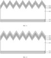
- FIG. 1 shows a schematic structural diagram of a solar cell according to some embodiments of the present disclosure.
- the solar cell includes: a substrate 100 having a front surface and a back surface opposite to the front surface; a first passivation layer 120, a second passivation layer 130 and a third passivation layer 140 sequentially formed on the front surface of the substrate 100 and in a direction away from the substrate 100; and a tunneling oxide layer 150 and a doped conductive layer 160 sequentially formed on the back surface of the substrate 100 and in a direction away from the back surface.
- the first passivation layer 120 includes a dielectric material.
- the second passivation layer 130 includes a first Si u N v material, and a value of v/u is 1.3 ⁇ v/u ⁇ 1.7.
- the third passivation layer 140 includes a Si r O s material, and a value of s/r is 1.9 ⁇ s/r ⁇ 3.2.
- the doped conductive layer 160 and the substrate 100 are doped to have a same conductivity type.
- the substrate 100 is used to receive incident light and generate photo-generated carriers.
- the substrate 100 may be a silicon substrate 100, and the material of the silicon substrate 100 may include at least one of monocrystalline silicon, polycrystalline silicon, amorphous silicon and microcrystalline silicon.
- the material of the substrate 100 may be a carbon simple substance, an organic material or a multi-component compound, and the multi-component compound includes gallium arsenide, cadmium telluride, copper indium selenium, etc.
- the solar cell is configured as a tunnel oxide passivated contact (TOPCON) solar cell.
- TOPCON tunnel oxide passivated contact
- the front surface and/or back surface of the substrate 100 can be used to receive the incident light.
- the front surface of the solar call may be designated as a main light-receiving surface that faces a light source (e.g., the sun).
- the front surface of the substrate 100 may be set as a pyramid textured surface, so that the front surface of the substrate 100 can have a relatively small reflectivity to the incident light, as well as a relatively large light absorption and utilization rate.
- the back surface of the substrate 100 may be set as a non-pyramid textured surface, such as a stacked and stepped morphology, to ensure that the tunneling oxide layer 150 on the back surface has relatively high density and uniformity, and accordingly the tunneling oxide layer 150 can have a good passivation effect on the back surface of the substrate 100.
- the substrate 100 is an N-type semiconductor substrate 100, that is, the substrate 100 is doped with N-type dopants (or doping elements), and the N-type dopants may include at least one of phosphorus, arsenic or antimony.
- the front surface of the substrate 100 is provided with an emitter 110.
- the emitter 110 may be a P-type doped layer doped with P-type dopants.
- the substrate 100 and the emitter 110 form a PN junction.
- the emitter 110 may be formed by doping and diffusing P-type dopants at a surface layer of the substrate 100, and a doped part of the substrate 100 severs as the emitter 110.
- the P-type dopants may be boron.
- a value of s/r is 1.9 ⁇ s/r ⁇ 3.2, where s represents the number of oxygen atoms (i.e., O atoms) and r represents the number of silicon atoms (i.e., Si atoms).
- s represents the number of oxygen atoms (i.e., O atoms)
- r represents the number of silicon atoms (i.e., Si atoms).
- the refractive index of the third passivation layer 140 is adjusted to match a refractive index of the second passivation layer 130, so that light reflection loss caused by poor refractive index matching between the third passivation layer 140 and the second passivation layer 130 can be reduced.
- a thickness of the third passivation layer 140 is adjusted to match with a wavelength of the incident light and the refractive index.
- the passivation layer can have better light transmission capacity, relatively strong light absorption capacity for the incident light, as well as better passivation effect.
- the wavelength of the incident light may be set to 632 nm.
- the third passivation layer 140 has relatively strong light absorption capacity for short-wave light.
- the third passivation layer 140 together with the second passivation layer 130 having the relatively strong light absorption capacity for long-wave light, allows the whole solar cell to have relatively strong light absorption capacity for the incident light (including short-wave light and long-wave light).
- a carrier concentration of the front surface of the substrate 100 of the solar cell can be increased, thus increasing an open-circuit voltage, a short-circuit current, and a filling factor of the solar cell, and improving the photoelectric conversion rate of the solar cell.
- the existing solar cells are generally blue, due to that the reflectivity of the passivation layer to the short-wave light is relatively high in the existing solar cells.
- the third passivation layer 140 since the third passivation layer 140 has relatively strong light absorption capacity for the short-wave light, a solar cell module including the solar cells may be grayish blue or even black, which is beneficial for preparing dark-colored solar cell modules.
- the refractive index of the third passivation layer 140 is lower than the refractive index of the second passivation layer 130. This may be achieved by adjusting the atomic ratio of the O atoms to the Si atoms in the Si r O s material of the third passivation layer 140.
- the third passivation layer 140 is an optically thinner medium
- the second passivation layer 130 is an optically denser medium. In a case that the incident light enters the optically denser medium from the optically thinner medium, an angle between the incident light and a normal line of the optically denser medium is relatively small because the refractive index of the optically denser medium is relatively large, so that the incident light may enter the substrate 100 at an angle close to vertical incidence.
- the refractive index of the Si r O s material in the third passivation layer 140 is lower than a refractive index of the first Si u N v material in the second passivation layer 130 intrinsically, the refractive index of the Si r O s material may be further decreased as compared with the refractive index of the first Si u N v material, by further adjusting the atomic ratio of the O atoms to the Si atoms in Si r O s material.
- the incident light may enter the second passivation layer 130 from the third passivation layer 140 at a more vertical angle, thereby further reducing the reflectivity of the solar cell to the incident light, increasing the carrier concentration on the front surface of the substrate 100 and improving the photoelectric conversion rate of the solar cell.
- the refractive index of the third passivation layer 140 is 1.4 ⁇ 1.6. Within this range, the refractive index of the Si r O s material is smaller than the refractive index of the first Si u N v material, and thus the refractive index of the third passivation layer 140 is smaller than the refractive index of the second passivation layer 130, thereby the solar cell can have relatively high light absorption and utilization rate for the incident light.
- the refractive index of the third passivation layer 140 is 1.4 ⁇ 1.6, the problem that the refractive index of the Si r O s material being too small may be avoided, so that the third passivation layer 140 can have a relatively strong anti-reflection effect on the incident light, and further improve the utilization rate of the incident light.
- the thickness of the third passivation layer 140 may be determined according to the incident light and the refractive index, by adjusting the atomic ratio of the O atoms to the Si atoms in the Si r O s material, so as to achieve better passivation effect and light transmission capacity of the solar cell.
- the thickness of the third passivation layer 140 is enabled to match the thickness of the second passivation layer 130, so that the front surface of the substrate 100 of the solar cell can have a relatively good overall passivation effect.
- the third passivation layer 140 has a thickness of 60 nm ⁇ 90 nm in a direction perpendicular to the front surface. In this way, the third passivation layer 140 has good light transmission capacity and is capable for absorbing more short-wave light. In addition, the third passivation layer 140 within this thickness range also has a good passivation effect, which not only allows a relatively high carrier concentration on the front surface of the substrate 100 of the solar cell, but also inhibits the recombination of carriers on the front surface of the substrate 100, thereby increasing the open-circuit voltage and short-circuit current of the solar cell and further increasing the photoelectric conversion rate of the solar cell.
- the atomic ratio of the O atoms to the Si atoms may be 1.9 ⁇ s/r ⁇ 2.2.
- the third passivation layer 140 may have a refractive index of 1.51-1.6, and a thickness of 60 nm ⁇ 67 nm.
- the atomic ratio of the O atoms to the Si atoms may be 2.2 ⁇ s/r ⁇ 2.5.
- the third passivation layer 140 may have a refractive index of 1.47 ⁇ 1.51, and a thickness of 67 nm ⁇ 74 nm.
- the atomic ratio of the O atoms to the Si atoms may also be 2.5 ⁇ s/r ⁇ 2.7.
- the third passivation layer 140 may have a refractive index of 1.45 ⁇ 1.47, and a thickness of 74 nm ⁇ 79 nm.
- the atomic ratio of the O atoms to the Si atoms may be 2.7 ⁇ s/r ⁇ 3.2.
- the third passivation layer 140 may have a refractive index of 1.4 ⁇ 1.45, and a thickness of 79 nm ⁇ 90 nm.
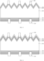
- the third passivation layer 140 may have a double-layer structure, including a first silicon oxide sub-layer 141 and a second silicon oxide sub-layer 142 stacked in the direction away from the substrate 100. Both the first silicon oxide sub-layer 141 and the second silicon oxide sub-layer 142 include the Si r O s material.
- the value of s/r of the Si r O s material in the first silicon oxide sub-layer 141 is 1.9 ⁇ s/r ⁇ 2.2; the value of s/r of Si r O s material in the second silicon oxide sub-layer 142 is 2.2 ⁇ s/r ⁇ 3.2, and a refractive index of the first silicon oxide sub-layer 141 is greater than a refractive index of the second silicon oxide sub-layer 142.
- the first silicon oxide sub-layer 141 and the second silicon oxide sub-layer 142 are provided, and the refractive index of the first silicon oxide sub-layer 141 is greater than the refractive index of the second silicon oxide sub-layer 142, so that reflection times and interference times of the incident light in the third passivation layer 140 may be increased, and absorption of the incident light by the third passivation layer 140 may be increased to a greater extent, thus achieving a good anti-reflection effect of the third passivation layer 140.
- Both the first silicon oxide sub-layer 141 and the second silicon oxide sub-layer 142 include the Si r O s material.
- the refractive indices of the first silicon oxide sub-layer 141 and the second silicon oxide sub-layer 142 are adjusted by adjusting the atomic ratio of the O atoms to the Si atoms in the Si r O s material, so that the refractive index of the first silicon oxide sub-layer 141 is larger than the refractive index of the second silicon oxide sub-layer 142.
- the thickness of the first silicon oxide sub-layer 141 is set to match the refractive index of the first silicon oxide sub-layer 141
- the thickness of the second silicon oxide sub-layer 142 is set to match the refractive index of the second silicon oxide sub-layer 142; so that both the first silicon oxide sub-layer 141 and the second silicon oxide sub-layer 142 can have good passivation effect.
- the first silicon oxide sub-layer 141 may have a refractive index of 1.51-1.6, such as 1.53 ⁇ 1.6. Accordingly, for the Si r O s material of the first silicon oxide sub-layer 141, the atomic ratio of the O atoms to the Si atoms may be 1.9 ⁇ s/r ⁇ 2.1, and the thickness of the first silicon oxide sub-layer 141 may be 30 nm ⁇ 40 nm.
- the second silicon oxide sub-layer 142 may have a refractive index of 1.4 ⁇ 1.51, such as 1.4 ⁇ 1.47.
- the atomic ratio of the O atoms to the Si atoms may be 2.4 ⁇ s/r ⁇ 3.2, and the thickness of the second silicon oxide sub-layer 142 may be 30 nm ⁇ 50 nm.
- the third passivation layer 140 may have a three-layer structure, including a first silicon oxide sub-layer 141, a second silicon oxide sub-layer 142 and a third silicon oxide sub-layer 143 stacked in the direction away from the substrate 100.
- the first silicon oxide sub-layer 141, the second silicon oxide sub-layer 142 and the third silicon oxide sub-layer 143 all include the Si r O s material. Refractive indices of the first silicon oxide sub-layer 141, the second silicon oxide sub-layer 142, and the third silicon oxide sub-layer 143 gradually decrease.
- the atomic ratio of the O atoms to the Si atoms may be 1.9 ⁇ s/r ⁇ 2.2, such as 1.9 ⁇ s/r ⁇ 2.1.
- the first silicon oxide sub-layer 141 may have a refractive index of 1.51 ⁇ 1.6, such as 1.53 ⁇ 1.6, and a thickness of 10 nm ⁇ 20 nm.
- the Si r O s material of the second silicon oxide sub-layer 142 the atomic ratio of the O atoms to the Si atoms may be 2.2 ⁇ s/r ⁇ 2.7, such as 2.2 ⁇ s/r ⁇ 2.5.
- the second silicon oxide sub-layer 142 may have a refractive index of 1.45 ⁇ 1.51, such as 1.46 ⁇ 1.51, and a thickness of 20 nm ⁇ 30 nm.
- the atomic ratio of the O atoms to the Si atoms may be 2.7 ⁇ s/r ⁇ 3.2, such as 2.9 ⁇ s/r ⁇ 3.2.
- the third silicon oxide sub-layer 143 may have a refractive index of 1.4 ⁇ 1.45, such as 1.4 ⁇ 1.43, and a thickness of 30 nm ⁇ 40 nm.
- the overall refractive index of the third passivation layer 140 is in the range of 1.4-1.6, regardless of whether the third passivation layer 140 is a single-layer structure or a multi-layer structure, so that the refractive index of the third passivation layer 140 matches the refractive index of the second passivation layer 130, and thus the substrate 100 can have relatively strong light absorption capacity for the incident light. It can be understood that under the condition that the overall refractive index of the third passivation layer 140 is in the range of 1.4-1.6, the overall thickness of the third passivation layer 140 is in the range of 60 nm ⁇ 90 nm regardless of whether the third passivation layer 140 is the single-layer structure or the multi-layer structure.
- the first Si u N v material of the second passivation layer 130 has a relatively high refractive index, so a Si-H bond density in the first Si u N v material is relatively high, which makes the first Si u N v material have a good passivation effect.
- the second passivation layer 130 may bring certain light absorption loss due to the relatively high refractive index of the first Si u N v material, that is, the second passivation layer 130 may have poor anti-reflection capacity to the incident light.
- the third passivation layer 140 is provided on a side of the second passivation layer 130 away from the substrate 100, and the Si r O s material of the third passivation layer 140 has a relatively small refractive index.
- the relatively high refractive index of the second passivation layer 130 optically matches the relatively low refractive index of the third passivation layer 140, so as to improve the light absorption capacity of the substrate 100 to the incident light.
- the second passivation layer 130 mainly absorbs long-wave light
- the third passivation layer 140 mainly absorbs short-wave light, so that the solar cell can have good light absorption capacity for the incident light in different wave bands.
- a value of v/u is 1.3 ⁇ v/u ⁇ 1.7, where the v represents the number of nitrogen atoms (i.e., N atoms) and the u represents the number of Si atoms.
- the refractive index of the second passivation layer 130 is adjusted to be greater than the refractive index of the third passivation layer 140. In this way, the incident light may be incident from the third passivation layer 140 to the second passivation layer 130 at a nearly vertical angle, so as to improve the utilization of the incident light.
- the second passivation layer 130 may have a single-layer structure, and the second passivation layer 130 may have a refractive index of 1.8 ⁇ 2.
- An optical matching performance between the refractive index of the second passivation layer 130 and the refractive index of the third passivation layer 140 is good within this refractive index range, so that the substrate 100 can have relatively strong light absorption capacity for the incident light, thereby reducing the reflectivity of the solar cell for the incident light.
- the refractive index of the second passivation layer 130 may not be too low within this refractive index range, so that reflected light or emitting light from the first passivation layer 120 may re-enter the substrate 100 due to the second passivation layer 130.
- the second passivation layer 130 within this refractive index range may have good passivation effect, and decreased interface state defects on the front surface of the substrate 100, thereby inhibiting the recombination of carriers on the front surface of the substrate 100 and improving the photoelectric conversion rate of the solar cell.
- the thickness of the second passivation layer 130 is set to match the refractive index of the second passivation layer 130, so that the second passivation layer 130 can have good light absorption capacity of incident light and good passivation effect.
- the thickness of the second passivation layer 130 is also set to adapt to the overall thickness of the solar cell. The overall thickness of the solar cell is prevented from being too thin, which may lead to breakage. The overall thickness of the solar cell is also prevented from being too thick, which may lead to difficulty in packaging.
- the thickness of the second passivation layer 130 may be adjusted by adjusting the atomic ratio of the Si atoms to the N atoms of the first Si u N v material of the second passivation layer 130.
- the second passivation layer 130 has a thickness of 35 nm ⁇ 55 nm in a direction perpendicular to the front surface. Within this thickness range, the thickness of the second passivation layer 130 is not too thin, so that the second passivation layer 130 can have a good refraction effect on the incident light, thus avoiding the problem that the incident light may be emitted through other passivation layers or emitted out of the substrate 100 before being absorbed by the substrate 100 due to the second passivation layer 130 being too thin. On the other hand, the number of positive charges in the second passivation layer 130 can achieve the hydrogen passivation effect within this thickness range, thereby further inhibiting the recombination of carriers on the front surface of the substrate 100.
- the atomic ratio of the N atoms to the Si atoms may be 1.3 ⁇ v/u ⁇ 1.4.
- the second passivation layer 130 may have a refractive index of 1.93 ⁇ 2, and a thickness of 35 nm ⁇ 40 nm.
- the atomic ratio of the N atoms to the Si atoms may be 1.4 ⁇ v/u ⁇ 1.55.
- the second passivation layer 130 may have a refractive index of 1.87 ⁇ 1.93, and a thickness of 40 nm ⁇ 48 nm.
- the atomic ratio of the N atoms to the Si atoms is 1.55 ⁇ v/u ⁇ 1.65.
- the second passivation layer 130 may have a refractive index of 1.84 ⁇ 1.87, and a thickness of 48 nm ⁇ 53 nm.
- the atomic ratio of the N atoms to the Si atoms may be 1.65 ⁇ v/u ⁇ 1.7.
- the second passivation layer 130 may have a refractive index of 1.8 ⁇ 1.84, and a thickness of 53 nm ⁇ 55 nm.
- the second passivation layer 130 may have a three-layer structure, including a first silicon nitride sub-layer 131, a second silicon nitride sub-layer 132 and a third silicon nitride sub-layer 133 stacked in the direction away from the substrate 100.
- the refractive indices of the first silicon nitride sub-layer 131, the second silicon nitride sub-layer 132 and the third silicon nitride sub-layer 133 gradually decrease.
- the first silicon nitride sub-layer 131, the second silicon nitride sub-layer 132 and the third silicon nitride sub-layer 133 all include the first Si u N v material.
- long-wave photons in the long-wave light may be reflected and interfered many times in the second passivation layer 130.
- the utilization ratio of the long-wave photons can be increased to a greater extent, and the long-wave response can be improved, so that more long-wave light can be absorbed in the solar cell.
- the refractive indices and thicknesses of the first silicon nitride sub-layer 131, the second silicon nitride sub-layer 132 and the third silicon nitride sub-layer 133 are adjusted by adjusting the atomic ratio of the N atoms to the Si atoms in the first Si u N v material of the first silicon nitride sub-layer 131, the second silicon nitride sub-layer 132 and the third silicon nitride sub-layer 133 respectively.
- the atomic ratio of the N atoms to the Si atoms of the first Si u N v material of the first silicon nitride sub-layer 131 may be adjusted to be 1.3 ⁇ v/u ⁇ 1.4.
- the atomic ratio of the N atoms to the Si atoms in the first Si u N v material of the second silicon nitride sub-layer 132 may be adjusted to be 1.4 ⁇ v/u ⁇ 1.55.
- the atomic ratio of the N atoms to the Si atoms of the first Si u N v material of the third silicon nitride sub-layer 133 may be adjusted to be 1.55 ⁇ v/u ⁇ 1.7.
- the first silicon nitride sub-layer 131 may have a refractive index of 1.93 ⁇ 2 and a thickness of 8 nm ⁇ 15 nm.
- the second silicon nitride sub-layer 132 may have a refractive index of 1. 87 ⁇ 1.93, such as 1.88 ⁇ 1.9. Accordingly, for the second silicon nitride layer 132, the atomic ratio of the N atoms to the Si atoms of the first Si u N v material may be 1.43 ⁇ v/u ⁇ 1.52, and the thickness may be 10 nm ⁇ 15 nm.
- the third silicon nitride sub-layer 133 may have a refractive index of 1.8 ⁇ 1.87, such as 1.8 ⁇ 1.84.
- the atomic ratio of the N atoms to the Si atoms of the first Si u N v material may be 1.59 ⁇ v/u ⁇ 1.7, and the thickness may be 17 nm ⁇ 25 nm.
- the second passivation layer 130 may have a four-layer structure, including a first silicon nitride sub-layer 131, a second silicon nitride sub-layer 132, a third silicon nitride sub-layer 133 and a fourth silicon nitride sub-layer stacked in the direction away from the substrate 100.
- the first silicon nitride sub-layer 131, the second silicon nitride sub-layer 132, the third silicon nitride sub-layer 133 and the fourth silicon nitride sub-layer all include the first Si u N v material.
- the refractive indices of the first silicon nitride sub-layer 131, the second silicon nitride sub-layer 132, the third silicon nitride sub-layer 133, and the fourth silicon nitride sub-layer gradually decrease.
- the atomic ratio of the N atoms to the Si atoms may be 1.3 ⁇ v/u ⁇ 1.4, such as 1.3 ⁇ v/u ⁇ 1.36.
- the first silicon nitride sub-layer 131 may have a refractive index of 1.93 ⁇ 2, such as 1.96 ⁇ 2, and a thickness of 8 nm ⁇ 13 nm.
- the atomic ratio of the N atoms to the Si atoms may be 1.4 ⁇ v/u ⁇ 1.55, such as 1.43 ⁇ v/u ⁇ 1.52.
- the second silicon nitride sub-layer 132 may have a refractive index of 1. 87 ⁇ 1.93, such as 1.89 ⁇ 1.92, and a thickness of 8 nm ⁇ 13 nm.
- the atomic ratio of the N atoms to the Si atoms may be 1.55 ⁇ v/u ⁇ 1.65, such as 1.57 ⁇ v/u ⁇ 1.63.
- the third silicon nitride sub-layer 133 may have a refractive index of 1.84 ⁇ 1.87, such as 1.85 ⁇ 1.86, and a thickness of 9 nm ⁇ 14 nm.
- the atomic ratio of the N atoms to the Si atoms may be 1.65 ⁇ v/u ⁇ 1.7, such as 1.67 ⁇ v/u ⁇ 1.7.
- the fourth silicon nitride sub-layer may have a refractive index of 1.8 ⁇ 1.84, such as 1.8 ⁇ 1.83, and a thickness of 10 nm ⁇ 15 nm.
- the refractive index of the second passivation layer 130 is in the range of 1.8 ⁇ 2, regardless of whether the second passivation layer 130 has the single-layer structure or the multi-layer structure. In this way, the refractive index of the second passivation layer 130 optically matches the refractive index of the third passivation layer 140, so that the reflectivity of the front surface of the substrate 100 to the incident light is relatively low, and the light absorption capacity of the substrate to the incident light is relatively strong.
- the overall thickness of the second passivation layer 130 is in the range of 35 nm ⁇ 55 nm regardless of whether the second passivation layer 130 has the single-layer structure or the multi-layer structure.
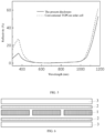
- the solar cell provided by the embodiments of the present disclosure has a lower reflectivity in the short-wave range (e.g., an ultraviolet light or near ultraviolet light) than a conventional TOPCON solar cell.
- the conventional TOPCON solar cell generally uses an aluminum oxide/silicon nitride stacked layer as a front passivation layer. Taking light at a wavelength of 360 nm as an example, a reflectivity of the conventional TOPCON solar cell is about 27%, and a reflectivity of the solar cell provided by the embodiments of the present disclosure is about 11.2%, which is reduced by about 58%.
- the solar cell provided by the embodiments of the present disclosure may be grayish blue, since the reflectivity of light is relatively low in the short-wave range, which is beneficial for preparing a dark-colored solar cell module.
- the solar cell provided by the embodiments of the present disclosure also has a greatly lower average reflectivity for the light at a wavelength range of 380 nm ⁇ 1050 nm.
- the average reflectivity of the conventional TOPCON solar cell for the light at the wavelength range of 380 nm ⁇ 1050 nm is 2.2%, while the average reflectivity of the solar cell provided by the embodiments of the present disclosure is 1.3%, which is reduced by about 41%.
- a TOPCON solar cell including the first passivation layer 120, the second passivation layer 130, and the third passivation layer 140 in the present embodiments has a short-circuit current increased by more than 70mA
- the first passivation layer 120 is required to have a good passivation effect.
- the dielectric material of the first passivation layer 120 may include at least one of aluminum oxide, titanium oxide, gallium oxide and hafnium oxide. It is worth noting that the aluminum oxide, the titanium oxide, the gallium oxide and the hafnium oxide are field passivation materials, which have a field passivation effect on the front surface of the substrate 100.
- a field passivation refers to forming a built-in electric field at an interface of the substrate 100 to reduce the concentration of electrons or holes at the interface of the substrate 100, thus achieving the surface passivation effect. This built-in electric field may generally be obtained by providing fixed electrical charges at the interface of the substrate 100.
- the dielectric material may be Al x O y material, and a value of y/x is 1.4 ⁇ y/x ⁇ 1.6, where y represents the number of O atoms and x represents the number of aluminum atoms (i.e., Al atoms).
- the Al x O y material has a good field passivation effect, because the Al x O y material may provide a sufficient number of fixed negative electrical charges.
- the built-in electric field may be formed at the front surface of the substrate 100, so as to reduce a minority carrier concentration at the front surface of the substrate 100 and inhibit the recombination of carriers, thereby improving the open-circuit voltage and short-circuit current of the solar cell.
- the Al x O y material further has a certain chemical passivation effect, that is, the recombination rate of carriers can be suppressed by reducing the number of defects on the front surface of the substrate 100.
- the refractive index and thickness of the first passivation layer 120 are adjusted by adjusting the atomic ratio of the O atoms to the Al atoms, so that the refractive index and thickness of the first passivation layer 120 are optimized and the first passivation layer 120 has a good passivation effect.
- the first passivation layer 120 has a refractive index of 1.6 ⁇ 1.8. In this refractive index range, the refractive index of the first passivation layer 120 matches the refractive index of the second passivation layer 130, thus reducing the light reflection loss caused by poor refractive index matching between the first passivation layer 120 and the second passivation layer 130, so that the first passivation layer 120 can have good light absorption capacity for the incident light.
- a thickness of the first passivation layer 120 may be determined to enable the thickness of the first passivation layer 120 to match the refractive index, so that the first passivation layer 120 can have good passivation effect.
- the first passivation layer 120 has a thickness of 2 nm ⁇ 8 nm in the direction perpendicular to the front surface. In this case, the first passivation layer 120 has relatively strong electronegativity, so that a selective transmission of carriers can be realized.
- the thickness of the first passivation layer 120 is related to the field passivation effect.
- the thickness of the first passivation layer 120 is adjusted within this ratio range, which can not only make the first passivation layer 120 have good field passivation effect, but also avoid the problem that the substrate 100 is damaged by stress due to excessive thickness.
- the atomic ratio of the O atoms to the Al atoms may be 1.4 ⁇ y/x ⁇ 1.42.
- the first passivation layer 120 may have a refractive index of 1.78 ⁇ 1.8, and a thickness of 2 nm ⁇ 2.6 nm.
- the atomic ratio of the O atoms to the Al atoms may be 1.42 ⁇ y/x ⁇ 1.48.
- the first passivation layer 120 may have a refractive index of 1.72 ⁇ 1.78, and a thickness of 2.6 nm ⁇ 4.4 nm.
- the atomic ratio of the O atoms to the Al atoms may be 1.48 ⁇ y/x ⁇ 1.55.
- the first passivation layer 120 may have a refractive index of 1.65 ⁇ 1.72, and a thickness of 4.4 nm ⁇ 6.5 nm.
- the atomic ratio of the O atoms to the Al atoms may be 4 ⁇ y/x ⁇ 7.
- the first passivation layer 120 may have a refractive index of 1.6 ⁇ 1.65, and a thickness of 6.5nm ⁇ 8nm.
- the tunneling oxide layer 150 and the doped conductive layer 160 are formed on the back surface of the substrate 100 as a passivation contact structure, and the tunneling oxide layer 150 is used to achieve interface passivation on the back surface.
- the material of the tunneling oxide layer 150 may be a dielectric material, such as silicon oxide.
- the doped conductive layer 160 is used to achieve field passivation.
- the doped conductive layer 160 and the substrate 100 are doped to have a same conductivity type.
- the doped conductive layer 160 and the substrate 100 may be doped with same dopants (or doping elements) or different dopants.
- the doped conductive layer 160 may be at least one of an N-type doped polycrystalline silicon layer, an N-type doped microcrystalline silicon layer and an N-type doped amorphous silicon layer.
- the doped conductive layer 160 includes N-type dopants, such as at least one of phosphorus, arsenic or antimony.
- the doped conductive layer 160 is a doped polycrystalline silicon layer.
- the doped conductive layer 160 has a thickness of 60nm ⁇ 150 nm in the direction perpendicular to the back surface, such as 60 nm, 80 nm or 120 nm.
- the solar cell includes a fourth passivation layer 170, which is disposed on a side of the doped conductive layer 160 facing away from the substrate 100.
- the fourth passivation layer 170 includes a second Si m N n material, and a value of n/m is 1.2 ⁇ y/x ⁇ 1.6.
- the fourth passivation layer 170 is used to enhance the reflection effect of the incident light on the back of the solar cell, and further to enhance the passivation effect of the passivation contact structure on the back surface of the substrate 100.
- n represents the number of N atoms
- m represents the number of Si atoms.
- a refractive index and thickness of the fourth passivation layer 170 may be adjusted by adjusting the value of n/m.
- the fourth passivation layer 170 has a single-layer structure.
- the fourth passivation layer 170 may have a refractive index of 1.9 ⁇ 2.1, and a thickness of 80 nm ⁇ 100 nm.
- the fourth passivation layer 170 may have a multi-layer structure.
- the refractive index of each sub-layer of the fourth passivation layer 170 gradually decreases in a direction from the back surface of the substrate 100 toward the doped conductive layer 160, so that it is beneficial to enhance the reflection effect of the incident light on a back of the solar cell by internal reflection.
- the solar cell further includes a first electrode 180 and a second electrode 190.
- the first electrode 180 is disposed on the front surface of the substrate 100 and is electrically connected with the emitter 110 by penetrating through the third passivation layer 140, the second passivation layer 130 and the first passivation layer 120.
- the second electrode 190 is disposed on the back surface of the substrate 100 and is electrically connected with the doped conductive layer by penetrating through the fourth passivation layer 170.
- the solar cell includes the first passivation layer 120, the second passivation layer 130 and the third passivation layer 140 sequentially formed on the front surface of the substrate 100 and in the direction away from the substrate 100.
- the first passivation layer 120 includes the dielectric material.
- the second passivation layer 130 includes the first Si u N v material, and the value of v/u is 1.3 ⁇ v/u ⁇ 1.7.
- the second passivation layer has relatively high refractive index by adjusting the atomic ratio in the first Si u N v material, so that the second passivation layer can have relatively strong light absorption capacity for long-wave light.
- the third passivation layer 140 includes the Si r O s material, and the value of s/r is 1.9 ⁇ s/r ⁇ 3.2.
- the Si r O s material can have relatively strong light absorption capacity for short-wave light by adjusting the atomic ratio in the Si r O s material.
- the third passivation layer 140 together with the second passivation layer, allows the whole solar cell have relatively strong light absorption capacity for the incident light (including short-wave light and long-wave light), and thus the anti-reflectivity of the solar cell surface can be relatively large.
- the first Si u N v material and the Si r O s material have a good passivation effect, thereby increasing improving the open-circuit voltage, the short-circuit current and the filling factor of the solar cell and improving the photoelectric conversion rate of the solar cell.
- some embodiments of the present disclosure further provide a solar cell module, including: at least one cell string formed by connecting a plurality of the solar cells 1 provided by the above embodiments; a packaging layer 2 configured to cover a surface of the at least one cell string; and a cover plate 3 configured to cover a surface of the packaging layer 2 away from the at least one cell string.
- the solar cells are electrically connected in a form of a whole piece or multiple pieces (for example, 1/2 equal pieces, 1/3 equal pieces, 1/4 equal pieces and other multiple pieces) to form a plurality of cell strings, and the plurality of cell strings are electrically connected in series and/or parallel.
- the plurality of cell strings may be electrically connected through conductive ribbons.
- the packaging layer 2 covers the front surface and the back surface of the solar cell.
- the packaging layer 2 on the back surface of the solar cell may be white. In this way, in a case that incident light incident from the front surface of the solar cell is irradiated to the back of the solar cell from a gap between two adjacent solar cell, the incident light may be reflected to the cover plate 3 on the front surface of the solar cells through the white packaging layer 2, and then reflected to the front surface of the solar cell once again, thus increasing the light absorption capacity of the incident light.
- the packaging layer 2 may be made of organic materials such as ethylene-vinyl acetate copolymer (EVA), polyolefin thermoplastic elastomer (POE) or polyethylene glycol terephthalate (PET).
- EVA ethylene-vinyl acetate copolymer
- POE polyolefin thermoplastic elastomer
- PET polyethylene glycol terephthalate
- the cover plate 3 may be a cover plate with a light-transmitting function, such as a glass cover plate, a plastic cover plate, and the like.
- a surface of the cover plate facing the packaging layer 2 may be a concave-convex surface, thereby increasing the utilization rate of the incident light.
- the solar cell of the present solar cell module includes a first passivation layer 120, a second passivation layer 130 and a third passivation layer 140 sequentially formed on the front surface.
- the second passivation layer 130 mainly absorbs long-wave light and the third passivation layer 140 mainly absorbs short-wave light, so that the solar cell has relatively strong light absorption capacity for incident light of different wave bands, thereby reducing a reflectivity of a front surface of a substrate 100 of the solar cell to light. Therefore, after the solar cells are packaged to form the solar cell module, the solar cell module is grayish blue or even black, which is beneficial for preparing a dark-colored solar cell module.
- some embodiments of the present disclosure further provide a method for preparing a solar cell, to prepare the solar cell provided in the above embodiments.
- the method will be described in detail with reference to the accompanying drawings.
- FIGs. 7 to 13 show schematic structural diagrams corresponding to each step of the method for preparing the solar cell according to some embodiments of the present disclosure.
- a substrate 100 having a front surface and a back surface opposite to the front surface is provided.
- the substrate 100 is used to receive incident light and generate photo-generated carriers.
- the substrate 100 may be a silicon substrate 100, and the materials of the silicon substrate 100 may include at least one of monocrystalline silicon, polycrystalline silicon, amorphous silicon and microcrystalline silicon.
- the material of the substrate 100 may be a carbon simple substance, an organic material or a multi-component compound.
- the multi-component compound includes gallium arsenide, cadmium telluride, copper indium selenium, etc.
- the solar cell is a tunnel oxide passivated contact (TOPCON) solar cell, and both the front surface and back surface of the substrate 100 are used to receive the incident light.
- TOPCON tunnel oxide passivated contact
- the front surface of the substrate 100 may be set as a pyramid textured surface, so that a reflectivity of the front surface of the substrate 100 to the incident light is relatively small, and thus the light absorption and utilization rate of the front surface of the substrate 100 is relatively large.
- the substrate 100 is an N-type semiconductor substrate, that is, the substrate 100 is doped with N-type dopants, and the N-type dopants may be any one of phosphorus, arsenic, or antimony.
- an emitter 110 is formed.
- the substrate 100 is the N-type semiconductor substrate, and the emitter 110 is a P-type emitter.
- a specific process method for forming the emitter 110 may be as follows. The front surface of the substrate 100 is subjected to a boron diffusion treatment to form the emitter 110. The emitter 110 and the N-type substrate 100 form a PN junction. It is worth noting that after the emitter 110 is formed, borosilicate glass formed by the boron diffusion treatment is required to be removed, so that when a first passivation layer 120 is subsequently formed on the emitter 110, the first passivation layer 120 has a uniform thickness, which is beneficial to improving the light absorption capacity of the front surface of the substrate 100 to the incident light.
- a boron source used in the boron diffusion treatment includes liquid boron tribromide.
- a tunneling oxide layer 150 and a doped conductive layer 160 are sequentially formed on the back surface of a substrate 100 in a direction away from the back surface.
- the doped conductive layer 160 and the substrate 100 are doped to have a same conductivity type.
- the tunneling oxide layer 150 is deposited on the back surface of the substrate 100 by using a temperature-variable process and a chemical vapor deposition process.
- the heating rate is controlled to be 0.5°C /min ⁇ 3°C /min, such as 1.0°C /min, 1.5°C /min, 2.0°C /min or 2.5°C /min, etc.
- the deposition temperature is 560°C ⁇ 620°C, such as 570°C, 590°C or 610°C, etc.
- the deposition time is 3 min ⁇ 10 min, such as 4 min, 6 min or 8 min, etc.
- the tunneling oxide layer 150 may be formed by an in-situ generation process, such as a thermal oxidation process or a nitric acid passivation process.
- the tunneling oxide layer 150 may have a thickness of 1 nm ⁇ 2 nm, such as 1.2 nm, 1.4 nm, 1.6 nm or 1.8 nm.
- a deposition process may be adopted to form the doped conductive layer 160 on a surface of the tunneling oxide layer 150.
- the deposition process may be adopted to deposit intrinsic polycrystalline silicon on the surface of the tunneling oxide layer 150 to form a polycrystalline silicon layer.
- phosphorus is doped to the polycrystalline silicon layer by an ion implantation and a source diffusion process to form an N-type doped polycrystalline silicon layer.
- the doped polycrystalline silicon layer serves as the doped conductive layer 160.
- the doped conductive layer 160 may have a thickness of 60 nm ⁇ 150 nm, such as 60 nm, 80 nm or 120 nm, in a direction perpendicular to the back surface of the substrate 100.
- the first passivation layer 120, a second passivation layer 130 and a third passivation layer 140 are sequentially formed on the front surface of a substrate 100 in a direction away from the substrate 100.
- the first passivation layer 120 includes a dielectric material.
- the second passivation layer 130 includes a first Si u N v material, and a value of v/u is 1.3 ⁇ v/u ⁇ 1.7.
- the third passivation layer 140 includes a Si r O s material, and a value of s/r is 1.9 ⁇ s/r ⁇ 3.2.
- the first passivation layer 120 is formed on the surface of the emitter 110.
- the first passivation layer 120 includes an Al x O y material.
- the first passivation layer 120 may be formed by an atomic layer deposition process.
- a method for forming the first passivation layer 120 includes introducing trimethyl aluminum and water into a reaction chamber, where a ratio of the trimethyl aluminum to the water is 1: 2 ⁇ 1: 3, and a temperature is 200°C ⁇ 300°C.
- the atomic ratio of O atoms to Al atoms of the Al x O y material is 1.4 ⁇ y/x ⁇ 1.6.
- the first passivation layer 120 has a refractive index of 1.6 ⁇ 1.8, and a thickness of 2 nm ⁇ 8 nm.
- the method further includes: performing an annealing process on the first passivation layer 120 in a nitrogen atmosphere, where an annealing temperature is 500°C ⁇ 600°C, and an annealing duration is 10 mim ⁇ 13 min. In this way, residual water molecules and organic functional groups can be removed.
- the second passivation layer 130 is formed on a surface of the first passivation layer 120, and the second passivation layer 130 includes the first Si u N v material.
- the second passivation layer 130 may be formed by a plasma-enhanced chemical vapor deposition process.
- a method for forming the second passivation layer includes: introducing silane and ammonia gas into a reaction chamber and ionizing the silane and the ammonia gas.
- a pulse power per unit area is 140mW/cm 2 ⁇ 180mW/cm 2 .
- a pressure of the reaction chamber is 1600 mTorr ⁇ 2000 mTorr.
- a flow ratio of the silane to the ammonia gas is 1:3 ⁇ 1:16, and a reaction time is 3s ⁇ 31s.
- the second passivation layer 130 may have a three-layer structure, and may include a first silicon nitride sub-layer 131 (refer to FIG. 4 ), a second silicon nitride sub-layer 132 (refer to FIG. 4 ), and a third silicon nitride sub-layer 133 (refer to FIG. 4 ) stacked in the direction away from the substrate 100.
- the process method for forming the second passivation layer 130 is as follows. The silane and the ammonia gas are introduced into a reaction chamber and ionized to form the first silicon nitride sub-layer 131 on the surface of the first passivation layer 120.
- the pulse power per unit area is 140mW/cm 2 ⁇ 170mW/cm 2 .
- the pressure of the reaction chamber is 1600 mTorrr ⁇ 2000 mTorr.
- the gas flow ratio of the silane to the ammonia gas may be 1:3 ⁇ 1:5, and the reaction time may be 4s ⁇ 6s.
- the silane and the ammonia gas are continuously introduced into the reaction chamber and ionized to form the second silicon nitride sub-layer 132 on a surface of the first silicon nitride sub-layer 131.
- the pulse power per unit area is 150mW/cm 2 ⁇ 180mW/cm 2 .
- the pressure of the reaction chamber is 1600 mTorrr ⁇ 2000 mTorr.
- the gas flow ratio of the silane to the ammonia gas may be 1:5 ⁇ 1:9, and the reaction time may be 5s ⁇ 8s.
- the silane and the ammonia gas are continuously introduced into the reaction chamber and ionized to form the third silicon nitride sub-layer 133 on a surface of the second silicon nitride sub-layer 132.
- the pulse power per unit area is 150mW/cm 2 ⁇ 180mW/cm 2 .
- the pressure of the reaction chamber is 1600 mTorrr ⁇ 2000 mTorr.
- the gas flow ratio of the silane to the ammonia gas may be 1:9 ⁇ 1:16, and the reaction time may be 10s ⁇ 14s.
- an atomic ratio of N atoms to Si atoms in the first silicon nitride sub-layer 131 is 1.3 ⁇ s/r ⁇ 1.4.
- the first silicon nitride sub-layer 131 has a refractive index of 1.93 ⁇ 2.0, and a thickness of 8 nm ⁇ 15 nm.
- the atomic ratio of the N atoms to the Si atoms in the second silicon nitride sub-layer 132 is 1.4 ⁇ s/r ⁇ 1.55.
- the second silicon nitride sub-layer 132 has a refractive index of 1. 87 ⁇ 1.93, and a thickness of 10 nm ⁇ 15 nm.
- the atomic ratio of the N atoms to the Si atoms in the third silicon nitride sub-layer 133 is 1.55 ⁇ s/r ⁇ 1.7.
- the third silicon nitride sub-layer 133 has a refractive index of 1.8 ⁇ 1.87, and a thickness of 17 nm ⁇ 25 nm.
- the second passivation layer 130 may have a four-layer structure, including the first silicon nitride sub-layer 131, the second silicon nitride sub-layer 132, the third silicon nitride sub-layer 133 and a fourth silicon nitride sub-layer stacked in the direction away from the substrate 100.
- the process method for forming the second passivation layer 130 is as follows. The silane and the ammonia gas are introduced into the reaction chamber and ionized to form the first silicon nitride sub-layer 131 on the surface of the first passivation layer 120.
- the pulse power per unit area is 140mW/cm 2 ⁇ 170mW/cm 2 .
- the pressure of the reaction chamber is 1600 mTorrr ⁇ 2000 mTorr.
- the gas flow ratio of the silane to the ammonia gas may be 1:3 ⁇ 1:5, and the reaction time may be 3s ⁇ 5s.
- the silane and the ammonia gas are continuously introduced into the reaction chamber and ionized to form the second silicon nitride sub-layer 132 on the surface of the first silicon nitride sub-layer 131.
- the pulse power per unit area is 150mW/cm 2 ⁇ 180mW/cm 2 .
- the pressure of the reaction chamber is 1600 mTorrr ⁇ 2000 mTorr.
- the gas flow ratio of the silane to the ammonia gas may be 1:5 ⁇ 1:7, and the reaction time may be 4s ⁇ 6s.
- the silane and the ammonia gas are continuously introduced into the reaction chamber and ionized to form the third silicon nitride sub-layer 133 on the surface of the second silicon nitride sub-layer 132.
- the pulse power per unit area is 150mW/cm 2 ⁇ 180mW/cm 2 .
- the pressure of the reaction chamber is 1600 mTorrr ⁇ 2000 mTorr.
- the gas flow ratio of the silane to the ammonia gas may be 1:7 ⁇ 1:10, and the reaction time may be 4s ⁇ 6s.
- the silane and the ammonia gas are continuously introduced into the reaction chamber and ionized to form the fourth silicon nitride sub-layer on a surface of the third silicon nitride sub-layer 133.
- the pulse power per unit area is 150mW/cm 2 ⁇ 180mW/cm 2 .
- the pressure of the reaction chamber is 1600 mTorrr ⁇ 2000 mTorr.
- the gas flow ratio of the silane to the ammonia gas may be 1:10 ⁇ 1:16, and the reaction time may be 10s ⁇ 14s.
- the third passivation layer 140 is formed on the surface of the second passivation layer 130, and the third passivation layer 140 includes the SirOs material.
- the third passivation layer 140 may be formed by the plasma-enhanced chemical vapor deposition process.
- a method for forming the third passivation layer 140 includes: introducing the silane and nitrous oxide into the reaction chamber and ionizing the silane and the nitrous oxide.
- the pulse power per unit area is 140mW/cm 2 ⁇ 170mW/cm 2 .
- the pressure of the reaction chamber is 1600 mTorr ⁇ 2000 mTorr.
- a flow ratio of the silane to the nitrous oxide is 1:15 ⁇ 1:20, and the reaction time is 3s ⁇ 22s.
- the third passivation layer 140 may have a two-layer structure, and may include a first silicon oxide sub-layer 141 (refer to FIG. 2 ) and a second silicon oxide sub-layer 142 (refer to FIG. 2 ) stacked in the direction away from the substrate 100.
- the process method for forming the third passivation layer 140 is as follows. The silane and the nitrous oxide are introduced into the reaction chamber and ionized to form the first silicon oxide sub-layer 141 on the surface of the second passivation layer 130.
- the pulse power per unit area is 140mW/cm 2 ⁇ 170mW/cm 2 .
- the pressure of the reaction chamber is 1600 mTorrr ⁇ 2000 mTorr.
- the gas flow ratio of the silane to the nitrous oxide may be 1:15 ⁇ 1:17, and the reaction time may be 6s ⁇ 8s.
- the silane and the nitrous oxide are continuously introduced into the reaction chamber and ionized to form the second silicon oxide sub-layer 142 on a surface of the first silicon oxide sub-layer 141.
- the pulse power per unit area is 140mW/cm 2 ⁇ 170mW/cm 2 .
- the pressure of the reaction chamber is 1600 mTorrr ⁇ 2000 mTorr.
- the gas flow ratio of the silane to the nitrous oxide may be 1:17 ⁇ 1:20, and the reaction time may be 6s ⁇ 10s.
- an atomic ratio of O atoms to Si atoms in the first silicon oxide sub-layer 141 is 1.9 ⁇ s/r ⁇ 2.2.
- the first silicon oxide sub-layer 141 has a refractive index of 1.51 ⁇ 1.6, and a thickness of 30 nm ⁇ 40 nm.
- the atomic ratio of the O atoms to the Si atoms in the second silicon oxide sub-layer 142 is 2.2 ⁇ s/r ⁇ 3.2.
- the second silicon oxide sub-layer 142 has a refractive index of 1.4 ⁇ 1.51, and a thickness of 30nm ⁇ 50nm.
- the third passivation layer 140 may have a three-layer structure, and may include the first silicon oxide sub-layer 141 (refer to FIG. 3 ), the second silicon oxide sub-layer 142 (refer to FIG. 3 ), and a third silicon oxide sub-layer 143 (refer to FIG. 3 ) stacked in the direction away from the substrate 100.
- the process method for forming the third passivation layer 140 is as follows. The silane and the nitrous oxide are introduced into the reaction chamber and ionized to form the first silicon oxide sub-layer 141 on the surface of the second passivation layer 130.
- the pulse power per unit area is 140mW/cm 2 ⁇ 170mW/cm 2 .
- the pressure of the reaction chamber is 1600 mTorrr ⁇ 2000 mTorr.
- the gas flow ratio of the silane to the nitrous oxide may be 1:15 ⁇ 1:16.5, and the reaction time may be 3s ⁇ 6s.
- the silane and the nitrous oxide are continuously introduced into the reaction chamber and ionized to form the second silicon oxide sub-layer 142 on the surface of the first silicon oxide sub-layer 141.
- the pulse power per unit area is 140mW/cm 2 ⁇ 170mW/cm 2 .
- the pressure of the reaction chamber is 1600 mTorrr ⁇ 2000 mTorr.
- the gas flow ratio of the silane to the nitrous oxide may be 1:16.5 ⁇ 1:18, and the reaction time may be 3s ⁇ 6s.
- the silane and the nitrous oxide are continuously introduced into the reaction chamber and ionized to form the third silicon oxide sub-layer 143 on a surface of the second silicon oxide sub-layer 141.
- the pulse power per unit area is 140mW/cm 2 ⁇ 170mW/cm 2 .
- the pressure of the reaction chamber is 1600 mTorrr ⁇ 2000 mTorr.
- the gas flow ratio of the silane to the nitrous oxide may be 1:18 ⁇ 1:20, and the reaction time may be 6s ⁇ 10s.
- the atomic ratio of the O atoms to the Si atoms in the first silicon oxide sub-layer 141 is 1.9 ⁇ s/r ⁇ 2.2.
- the first silicon oxide sub-layer 141 has a refractive index of 1.51 ⁇ 1.6, and a thickness of 10 nm ⁇ 20 nm.
- the atomic ratio of the O atoms to the Si atoms in the second silicon oxide sub-layer 142 is 2.2 ⁇ s/r ⁇ 2.7.
- the second silicon oxide sub-layer 142 has a refractive index of 1.45 ⁇ 1.51, and a thickness of 20 nm ⁇ 30 nm.
- the atomic ratio of the O atoms to the Si atoms in the third silicon oxide sub-layer 143 is 2.7 ⁇ s/r ⁇ 3.2.
- the third silicon oxide sub-layer 143 has a refractive index of 1.4 ⁇ 1.45, and a thickness of 30 nm ⁇ 40 nm.
- a fourth passivation layer 170 is formed on the doped conductive layer 160, and a first electrode 180 and a second electrode 190 are formed.
- the fourth passivation layer 170 includes a second Si m N n material.
- the fourth passivation layer 170 may be formed on a surface of the doped conductive layer 160 by using the plasma-enhanced chemical vapor deposition process.
- the fourth passivation layer 170 may have a single-layer structure.
- the fourth passivation layer 170 may have a multi-layer structure, and the refractive index of each layer gradually decreases in a direction from the back surface of the substrate 100 toward the doped conductive layer 160.
- a metallization treatment is performed on the surfaces of the third passivation layer 140 on the front surface of the substrate 100 and the fourth passivation layer 170 on the back surface of the substrate 100,.
- the metallization treatment includes a screen printing process and a high-temperature sintering process, so as to form the first electrode 180 electrically connected with the emitter 110 on the front surface of the substrate 100 and the second electrode 190 electrically connected with the doped conductive layer 160 on the back surface of the substrate 100.
- the first electrode 180 penetrates through the third passivation layer 140, the second passivation layer 130 and the first passivation layer 120 on the front surface of the substrate 100.
- the formed second electrode 190 penetrates through the fourth passivation layer 170.
- the first passivation layer 120, the second passivation layer 130 and the third passivation layer 140 are formed sequentially on the front surface of the substrate 100 and in the direction away from the substrate 100.
- the first passivation layer 120 includes the dielectric material.
- the second passivation layer 130 includes the first Si u N v material, and the value of v/u is 1.3 ⁇ v/u ⁇ 1.7.
- the second passivation layer has relatively high refractive index by adjusting the atomic ratio in the first Si u N v material, so that the second passivation layer has relatively strong light absorption capacity for long-wave light.
- the first Si u N v material in the second passivation layer 130 has good hydrogen passivation effect.
- the third passivation layer 140 includes the Si r O s material, and the value of s/r is 1.9 ⁇ s/r ⁇ 3.2.
- the Si r O s material can have relatively strong light absorption capacity for short-wave light by adjusting the atomic ratio in the Si r O s material. In this way, the third passivation layer 140, together with the relatively strong light, allows the whole solar cell have relatively strong light absorption capacity for the incident light (including short-wave light and long-wave light), and thus the anti-reflectivity of the solar cell surface can be relatively large.
- the first Si u N v material and the Si r O s material have a good passivation effect, thereby improving an open-circuit voltage, a short-circuit current and a filling factor of the solar cell and increasing the photoelectric conversion rate of the solar cell.
- the first comparative example provides a solar cell, as shown in FIG. 13 , including: a substrate 200 having a front surface and a back surface opposite to the front surface; a front passivation layer 220 formed on a front surface of the substrate 200.
- the front passivation layer includes a Si a N b material.
- the first comparative example differs from the embodiments of the present disclosure in that: a single-layered front passivation layer 220 is formed on the front surface of the substrate 200 in the first comparative example, and the material of the front passivation layer 220 is the Si a N b material.
- the solar cell includes the first passivation layer 120, the second passivation layer 130 and the third passivation layer 140 sequentially formed on the front surface of the substrate 100 in the direction away from the substrate 100.
- the first passivation layer 120 includes the dielectric material
- the second passivation layer 130 includes the first Si u N v material
- the third passivation layer 140 includes the Si r O s material. It is found through comparative experiments that the parameter comparison between the embodiments of the present disclosure and the first comparative example is shown in Table 1.
- Table 1 Reflectivity % Open-circuit voltage mV Short-circuit current A Filling factor % Conversion efficiency % Embodiments of the present disclosure 1.45 702 10.904 84.63 24.23 First comparative example 2.07 685 10.760 84.73 23.35
- the solar cell in the embodiments of the present disclosure has relatively lower reflectivity to incident light, and has relatively larger open-circuit voltage, short-circuit current and parallel resistance, so that the solar cell in the embodiments of the present disclosure has higher conversion efficiency.
- the reflectivity of the solar cell to the incident light is 0.62% lower than the reflectivity of the solar cell in the first comparative example, and the conversion efficiency of the solar cell is 0.88% higher than the conversion efficiency of the solar cell in the first comparative example.
- the front passivation layer 220 is the Si a N b material and is in a single-layered structure.
- the Si a N b material has a relatively high refractive index, which may bring certain light absorption loss and poor light absorption capacity for the incident light.
- the second passivation layer 130 is the first Si u N v material, for mainly absorbing long-wave light
- the third passivation layer is the Si r O s material, for mainly absorbing short-wave light, so that the solar cell has good light absorption capacity for the incident light in different wave bands, thus making the solar cell have relatively high utilization rate of the incident light, thereby increasing the carrier concentration on the front surface of the substrate 100 and improving the conversion efficiency of the solar cell.
- the second comparative example provides a solar cell, as shown in FIG. 14 , including: a substrate 300 having a front surface and a back surface opposite to the front surface; a first passivation layer 320 and a second passivation layer 330 sequentially formed on the front surface of the substrate 300 and in a direction away from the substrate 300.
- the first passivation layer 320 includes an A j O k material
- the second passivation layer 330 includes a Si p N q material.
- the second comparative example differs from the embodiments of the present disclosure in that: two passivation layers are formed on the front surface of the substrate 300 in the second comparative example.
- the solar cell includes the first passivation layer 120, the second passivation layer 130 and the third passivation layer 140 sequentially formed on the front surface of the substrate 100 in the direction away from the substrate 100.
- the first passivation layer 120 includes the dielectric material
- the second passivation layer 130 includes the first Si u N v material
- the third passivation layer 140 includes the Si r O s material.
- the solar cell in the embodiments of the present disclosure has relatively lower reflectivity to incident light, and has relatively larger open-circuit voltage, short-circuit current, filling factor and parallel resistance, so that the solar cell in the embodiments of the present disclosure has higher conversion efficiency.
- the reflectivity of the solar cell to the incident light is 0.68% lower than the reflectivity of the solar cell in the second comparative example, and the conversion efficiency of the solar cell is 0.25% higher than the conversion efficiency of the solar cell in the second comparative example.
- the second passivation layer 330 is the Si p N q material, so the solar cell in the second comparative example may merely have good absorption effect on long-wave light.
- the third passivation layer is the Si r O s material, for mainly absorbing short-wave light.
- the refractive index of the third passivation layer 140 is set to be lower than the refractive index of the second passivation layer 130, so that the incident light enters the optically denser medium from the optically thinner medium and enters the substrate 100 at a nearly vertical angle. Therefore, the utilization rate of the incident light is relatively high, thereby increasing the carrier concentration on the front surface of the substrate 100 and improving the conversion efficiency of the solar cell.
Landscapes
- Photovoltaic Devices (AREA)
- Life Sciences & Earth Sciences (AREA)
- Engineering & Computer Science (AREA)
- Sustainable Development (AREA)
- Sustainable Energy (AREA)
- Surface Treatment Of Optical Elements (AREA)
Abstract
Description
- Embodiments of the present disclosure relate to a photovoltaic technology, in particular to a solar cell, a method for preparing a solar cell and a solar cell module.
- A solar cell can be used widely due to a good photoelectric conversion capacity. The solar cell generally has a passivation structure on a surface of the solar cell in order to inhibit a recombination of carriers on the surface. The passivation structure on the surface of the solar cell has a relatively high refractive index and relatively good passivation effect, so that as much incident light as possible can be absorbed by the solar cell, and a carrier concentration of the solar cell can be increased.
- However, the existing solar cell with the passivation layer still has relatively high reflectivity for the incident light, so that the existing solar cell has a relatively low open circuit voltage, a low short-circuit current and a low filling factor, resulting in a relatively low photoelectric conversion rate of the solar cell.
- As one aspect, some embodiments of the present disclosure provide a solar cell, including: a substrate having a front surface and a back surface opposite to the front surface; a first passivation layer, a second passivation layer and a third passivation layer sequentially formed on the front surface of the substrate and in a direction away from the substrate; the first passivation layer includes a dielectric material; the second passivation layer includes a first SiuNv material, and a value of v/u is in a range of 1.3 to 1.7; and the third passivation layer includes a SirOs material, and a value of s/r is in a range of 1.9 to 3.2; and a tunneling oxide layer and a doped conductive layer sequentially formed on the back surface of the substrate and in a direction away from the back surface, the doped conductive layer and the substrate are doped to have a same conductivity type.
- In some examples, a refractive index of the third passivation layer is smaller than a refractive index of the second passivation layer.
- In some examples, the third passivation layer has a refractive index in a range of 1.4 to 1.6, and the second passivation layer has a refractive index in a range of 1.8 to 2.
- In some examples, the third passivation layer includes a first silicon oxide sub-layer and a second silicon oxide sub-layer stacked in the direction away from the substrate, the value of s/r of the SirOs material of the first silicon oxide sub-layer is in a range of 1.9 to 2.2; the value of s/r of the SirOs material of the second silicon oxide sub-layer is in a range of 2.2 to 3.2, and a refractive index of the first silicon oxide sub-layer is greater than a refractive index of the second silicon oxide sub-layer.
- In some examples, the dielectric material includes at least one of aluminum oxide, titanium oxide, gallium oxide and hafnium oxide.
- In some examples, the dielectric material is an AlxOy material, and a value of y/x is in a range of 1.4 to 1.6.
- In some examples, the third passivation layer has a thickness in a range of 60 nm to 90 nm in a direction perpendicular to the front surface.
- In some examples, the second passivation layer has a thickness in a range of 35 nm to 55 nm in a direction perpendicular to the front surface.
- In some examples, the first passivation layer has a thickness in a range of 2 nm to 8 nm in a direction perpendicular to the front surface.
- In some examples, the first passivation layer has a refractive index in a range of 1.6 to 1.8.
- In some examples, the solar cell further includes: a fourth passivation layer formed on a side of the doped conductive layer facing away from the substrate; the fourth passivation layer includes a second SimNn material, and a value of n/m is in a range of 1.2 to 1.6.
- In some examples, the fourth passivation layer has a refractive index in a range of 1.9 to 2.1, and the fourth passivation layer has a thickness in a range of 80 nm to 100 nm in a direction perpendicular to the back surface.
- In some examples, the substrate is an N-type semiconductor substrate; the doped conductive layer is at least one of an N-type doped polycrystalline silicon layer, an N-type doped microcrystalline silicon layer and an N-type doped amorphous silicon layer.
- As a second aspect, some embodiments of the present disclosure further provide a solar cell module, including: at least one cell string formed by connecting a plurality of the above solar cells; a packaging layer configured to cover a surface of the at least one cell string; and a cover plate configured to cover a surface of the packaging layer away from the at least one cell string.
- As a third aspect, some embodiments of the present disclosure further provide a method for preparing a solar cell, including: providing a substrate having a front surface and a back surface opposite to the front surface; forming a tunneling oxide layer and a doped conductive layer sequentially on the back surface of the substrate in a direction away from the back surface, the doped conductive layer and the substrate are doped to have a same conductivity type; and forming a first passivation layer, a second passivation layer and a third passivation layer sequentially on the front surface of the substrate and in a direction away from the substrate; the first passivation layer includes a dielectric material; the second passivation layer includes a first SiuNv material, and a value of v/u is in a range of 1.3 to 1.7; and the third passivation layer includes a SirOs material, and a value of s/r is in a range of 1.9 to 3.2.
- In some examples, the forming the third passivation layer is performed by a plasma-enhanced chemical vapor deposition process, and includes: introducing silane and nitrous oxide into a reaction chamber; and ionizing the silane and the nitrous oxide; a pulse power per unit area is in a range of 140mW/cm2 to 170mW/cm2, a pressure of the reaction chamber is in a range of 1600 mTorr to 2000 mTorr, a flow ratio of the silane to the nitrous oxide is in a range of 1:15 to 1:20; and a reaction time is in a range of 3s to 22s.
- In some examples, the forming the second passivation layer is performed by a plasma-enhanced chemical vapor deposition process, and includes: introducing silane and ammonia gas into a reaction chamber; and ionizing the silane and the ammonia gas; a pulse power per unit area is in a range of 140mW/cm2 to 180mW/cm2; a pressure of the reaction chamber is in a range of 1600 mTorr to 2000 mTorr; a flow ratio of the silane to the ammonia gas is in a range of 1:3 to 1:16; and a reaction time is in a range of 3s to 31s.
- In some examples, the forming the first passivation layer is performed by an atomic layer deposition process, and includes: introducing trimethyl aluminum and water into a reaction chamber, a ratio of the trimethyl aluminum to the water is in a range of 1:2 to 1:3, and a temperature is in a range of 200°C to 300°C.
- In some examples, after the first passivation layer is formed, the method further includes: performing an annealing process on the first passivation layer in a nitrogen atmosphere, an annealing temperature is in a range of 450°C to 550°C, and an annealing duration is in a range of 10 min to 13 min.
- One or more embodiments are described as examples with reference to the corresponding figures in the accompanying drawings, and the examples do not constitute a limitation to the embodiments. The figures in the accompanying drawings do not constitute a proportion limitation unless otherwise stated.
-
FIG. 1 shows a schematic structural diagram of a solar cell according to some embodiments of the present disclosure; -
FIG. 2 shows a schematic structural diagram of another solar cell according to some embodiments of the present disclosure; -
FIG. 3 shows a schematic structural diagram of yet another solar cell according to some embodiments of the present disclosure; -
FIG. 4 shows a schematic structural diagram of still another solar cell according to some embodiments of the present disclosure; -
FIG. 5 shows a wavelength-reflectivity comparison diagram according to some embodiments of the present disclosure; -
FIG. 6 shows a schematic structural diagram of a solar cell module according to some embodiments of the present disclosure; -
FIG. 7 to FIG. 12 show schematic structural diagrams corresponding to each step of a method for preparing a solar cell according to some embodiments of the present disclosure; -
FIG. 13 shows a schematic structural diagram of a solar cell according to a first comparative example of the present disclosure; -
FIG. 14 shows a schematic structural diagram of a solar cell according to a second comparative example of the present disclosure. - It can be known from the background technology that there exists a problem that a reflectivity of a solar cell to incident light is relatively high.
- It is found that one reason for the relatively high reflectivity of the solar cell to the incident light may be that: a silicon nitride material is generally used for a passivation layer on a surface of the solar cell; the silicon nitride material has a good passivation effect, but a relatively high refractive index, which results in certain light absorption loss. That is, a silicon nitride passivation layer may have a relatively low anti-reflectivity, resulting in a relatively weak light absorption capacity of the solar cell to the incident light.
- Some embodiments of the present disclosure provide a solar cell, including: a first passivation layer, a second passivation layer and a third passivation layer sequentially formed on a front surface of a substrate and in a direction away from the substrate. The first passivation layer includes a dielectric material. The second passivation layer includes a first SiuNv material, and a value of v/u is 1.3≤v/u≤1.7. The second passivation layer has a relatively high refractive index by adjusting an atomic ratio in the first SiuNv material, so that the second passivation layer has relatively strong light absorption capacity for long-wave light (e.g., an infrared light or near infrared light). The third passivation layer includes a SirOs material, and a value of s/r is 1.9≤s/r≤3.2. The SirOs material has relatively strong light absorption capacity for short-wave light by adjusting an atomic ratio in the SirOs material. In this way, the third passivation layer having relatively strong light absorption capacity for short-wave light, together with the second passivation layer having relatively strong light absorption capacity for short-wave light, allows the whole solar cell have relatively strong light absorption capacity for incident light, and thus the solar cell surface can have a relatively large anti-reflectivity. Further, the first SiuNv material and the SirOs material have a good passivation effect, thereby improving an open-circuit voltage, a short-circuit current and a filling factor of the solar cell and increasing a photoelectric conversion rate of the solar cell.
- Embodiments of the present disclosure will be described in detail below with reference to the accompanying drawings. However, those skilled in the art may appreciate that, in the various embodiments of the present disclosure, numerous technical details are set forth in order to provide the reader with a better understanding of the present disclosure. However, the technical solutions claimed in the present disclosure may be implemented without these technical details and various changes and modifications based on the following embodiments.
-
FIG. 1 shows a schematic structural diagram of a solar cell according to some embodiments of the present disclosure. - As shown in
FIG. 1 , the solar cell includes: asubstrate 100 having a front surface and a back surface opposite to the front surface; afirst passivation layer 120, asecond passivation layer 130 and athird passivation layer 140 sequentially formed on the front surface of thesubstrate 100 and in a direction away from thesubstrate 100; and atunneling oxide layer 150 and a dopedconductive layer 160 sequentially formed on the back surface of thesubstrate 100 and in a direction away from the back surface. Thefirst passivation layer 120 includes a dielectric material. Thesecond passivation layer 130 includes a first SiuNv material, and a value of v/u is 1.3≤v/u≤1.7. Thethird passivation layer 140 includes a SirOs material, and a value of s/r is 1.9≤s/r≤3.2. The dopedconductive layer 160 and thesubstrate 100 are doped to have a same conductivity type. - The
substrate 100 is used to receive incident light and generate photo-generated carriers. In some examples, thesubstrate 100 may be asilicon substrate 100, and the material of thesilicon substrate 100 may include at least one of monocrystalline silicon, polycrystalline silicon, amorphous silicon and microcrystalline silicon. In some examples, the material of thesubstrate 100 may be a carbon simple substance, an organic material or a multi-component compound, and the multi-component compound includes gallium arsenide, cadmium telluride, copper indium selenium, etc. In some examples, the solar cell is configured as a tunnel oxide passivated contact (TOPCON) solar cell. In some embodiments, the front surface and/or back surface of thesubstrate 100 can be used to receive the incident light. Generally, the front surface of the solar call may be designated as a main light-receiving surface that faces a light source (e.g., the sun). In some examples, the front surface of thesubstrate 100 may be set as a pyramid textured surface, so that the front surface of thesubstrate 100 can have a relatively small reflectivity to the incident light, as well as a relatively large light absorption and utilization rate. The back surface of thesubstrate 100 may be set as a non-pyramid textured surface, such as a stacked and stepped morphology, to ensure that thetunneling oxide layer 150 on the back surface has relatively high density and uniformity, and accordingly thetunneling oxide layer 150 can have a good passivation effect on the back surface of thesubstrate 100. - In some examples, the
substrate 100 is an N-type semiconductor substrate 100, that is, thesubstrate 100 is doped with N-type dopants (or doping elements), and the N-type dopants may include at least one of phosphorus, arsenic or antimony. The front surface of thesubstrate 100 is provided with anemitter 110. Theemitter 110 may be a P-type doped layer doped with P-type dopants. Thesubstrate 100 and theemitter 110 form a PN junction. In some examples, theemitter 110 may be formed by doping and diffusing P-type dopants at a surface layer of thesubstrate 100, and a doped part of thesubstrate 100 severs as theemitter 110. In some examples, the P-type dopants may be boron. - For the SirOs material of the
third passivation layer 140, a value of s/r is 1.9≤s/r≤3.2, where s represents the number of oxygen atoms (i.e., O atoms) and r represents the number of silicon atoms (i.e., Si atoms). By adjusting the atomic ratio of the O atoms to the Si atoms in the SirOs material, a refractive index of the SirOs material may be adjusted. In this way, the refractive index of thethird passivation layer 140 is adjusted to match a refractive index of thesecond passivation layer 130, so that light reflection loss caused by poor refractive index matching between thethird passivation layer 140 and thesecond passivation layer 130 can be reduced. On the other hand, a thickness of thethird passivation layer 140 is adjusted to match with a wavelength of the incident light and the refractive index. The thickness of the passivation layer, the refractive index of the passivation layer and the wavelength of the incident light shall satisfy a following formula: a wavelength of incident light = 4× thickness × refractive index. In this way, the passivation layer can have better light transmission capacity, relatively strong light absorption capacity for the incident light, as well as better passivation effect. In some examples, the wavelength of the incident light may be set to 632 nm. - In addition, by adjusting the atomic ratio of the O atoms to the Si atoms in the SirOs material, the
third passivation layer 140 has relatively strong light absorption capacity for short-wave light. Thethird passivation layer 140, together with thesecond passivation layer 130 having the relatively strong light absorption capacity for long-wave light, allows the whole solar cell to have relatively strong light absorption capacity for the incident light (including short-wave light and long-wave light). In this way, a carrier concentration of the front surface of thesubstrate 100 of the solar cell can be increased, thus increasing an open-circuit voltage, a short-circuit current, and a filling factor of the solar cell, and improving the photoelectric conversion rate of the solar cell. It is worth noting that the existing solar cells are generally blue, due to that the reflectivity of the passivation layer to the short-wave light is relatively high in the existing solar cells. However, in the present embodiments, since thethird passivation layer 140 has relatively strong light absorption capacity for the short-wave light, a solar cell module including the solar cells may be grayish blue or even black, which is beneficial for preparing dark-colored solar cell modules. - In some examples, the refractive index of the
third passivation layer 140 is lower than the refractive index of thesecond passivation layer 130. This may be achieved by adjusting the atomic ratio of the O atoms to the Si atoms in the SirOs material of thethird passivation layer 140. In this case, thethird passivation layer 140 is an optically thinner medium, and thesecond passivation layer 130 is an optically denser medium. In a case that the incident light enters the optically denser medium from the optically thinner medium, an angle between the incident light and a normal line of the optically denser medium is relatively small because the refractive index of the optically denser medium is relatively large, so that the incident light may enter thesubstrate 100 at an angle close to vertical incidence. In this way, more light may enter thesubstrate 100, and the reflectivity of the solar cell to the incident light may be relatively small. It is worth noting that although a refractive index of the SirOs material in thethird passivation layer 140 is lower than a refractive index of the first SiuNv material in thesecond passivation layer 130 intrinsically, the refractive index of the SirOs material may be further decreased as compared with the refractive index of the first SiuNv material, by further adjusting the atomic ratio of the O atoms to the Si atoms in SirOs material. As such, the incident light may enter thesecond passivation layer 130 from thethird passivation layer 140 at a more vertical angle, thereby further reducing the reflectivity of the solar cell to the incident light, increasing the carrier concentration on the front surface of thesubstrate 100 and improving the photoelectric conversion rate of the solar cell. - In some examples, the refractive index of the
third passivation layer 140 is 1.4~1.6. Within this range, the refractive index of the SirOs material is smaller than the refractive index of the first SiuNv material, and thus the refractive index of thethird passivation layer 140 is smaller than the refractive index of thesecond passivation layer 130, thereby the solar cell can have relatively high light absorption and utilization rate for the incident light. Moreover, since the refractive index of thethird passivation layer 140 is 1.4~1.6, the problem that the refractive index of the SirOs material being too small may be avoided, so that thethird passivation layer 140 can have a relatively strong anti-reflection effect on the incident light, and further improve the utilization rate of the incident light. - It can be understood that when the wavelength of the incident light and the refractive index of the
third passivation layer 140 are provided, the thickness of thethird passivation layer 140 may be determined according to the incident light and the refractive index, by adjusting the atomic ratio of the O atoms to the Si atoms in the SirOs material, so as to achieve better passivation effect and light transmission capacity of the solar cell. In addition, the thickness of thethird passivation layer 140 is enabled to match the thickness of thesecond passivation layer 130, so that the front surface of thesubstrate 100 of the solar cell can have a relatively good overall passivation effect. - In some examples, the
third passivation layer 140 has a thickness of 60 nm~90 nm in a direction perpendicular to the front surface. In this way, thethird passivation layer 140 has good light transmission capacity and is capable for absorbing more short-wave light. In addition, thethird passivation layer 140 within this thickness range also has a good passivation effect, which not only allows a relatively high carrier concentration on the front surface of thesubstrate 100 of the solar cell, but also inhibits the recombination of carriers on the front surface of thesubstrate 100, thereby increasing the open-circuit voltage and short-circuit current of the solar cell and further increasing the photoelectric conversion rate of the solar cell. - In some examples, for the SirOs material of the
third passivation layer 140, the atomic ratio of the O atoms to the Si atoms may be 1.9≤s/r≤2.2. Thethird passivation layer 140 may have a refractive index of 1.51-1.6, and a thickness of 60 nm~67 nm. In some examples, for the SirOs material of thethird passivation layer 140, the atomic ratio of the O atoms to the Si atoms may be 2.2≤s/r≤2.5. Thethird passivation layer 140 may have a refractive index of 1.47∼1.51, and a thickness of 67 nm~74 nm. In some examples, for the SirOs material of thethird passivation layer 140, the atomic ratio of the O atoms to the Si atoms may also be 2.5≤s/r≤2.7. Thethird passivation layer 140 may have a refractive index of 1.45~1.47, and a thickness of 74 nm~79 nm. In some examples, for the SirOs material of thethird passivation layer 140, the atomic ratio of the O atoms to the Si atoms may be 2.7≤s/r≤3.2. Thethird passivation layer 140 may have a refractive index of 1.4~1.45, and a thickness of 79 nm~90 nm. - As shown in
FIG. 2 , in some examples, thethird passivation layer 140 may have a double-layer structure, including a firstsilicon oxide sub-layer 141 and a second silicon oxide sub-layer 142 stacked in the direction away from thesubstrate 100. Both the firstsilicon oxide sub-layer 141 and the second silicon oxide sub-layer 142 include the SirOs material. Herein, the value of s/r of the SirOs material in the firstsilicon oxide sub-layer 141 is 1.9≤s/r≤2.2; the value of s/r of SirOs material in the second silicon oxide sub-layer 142 is 2.2≤s/r≤3.2, and a refractive index of the firstsilicon oxide sub-layer 141 is greater than a refractive index of the second silicon oxide sub-layer 142. - Compared with the
third passivation layer 140 having a single-layer structure, in the exemplary solar cell as show inFIG. 2 , the firstsilicon oxide sub-layer 141 and the second silicon oxide sub-layer 142 are provided, and the refractive index of the firstsilicon oxide sub-layer 141 is greater than the refractive index of the second silicon oxide sub-layer 142, so that reflection times and interference times of the incident light in thethird passivation layer 140 may be increased, and absorption of the incident light by thethird passivation layer 140 may be increased to a greater extent, thus achieving a good anti-reflection effect of thethird passivation layer 140. - Both the first
silicon oxide sub-layer 141 and the second silicon oxide sub-layer 142 include the SirOs material. The refractive indices of the firstsilicon oxide sub-layer 141 and the second silicon oxide sub-layer 142 are adjusted by adjusting the atomic ratio of the O atoms to the Si atoms in the SirOs material, so that the refractive index of the firstsilicon oxide sub-layer 141 is larger than the refractive index of the second silicon oxide sub-layer 142. The thickness of the firstsilicon oxide sub-layer 141 is set to match the refractive index of the firstsilicon oxide sub-layer 141, and the thickness of the second silicon oxide sub-layer 142 is set to match the refractive index of the second silicon oxide sub-layer 142; so that both the firstsilicon oxide sub-layer 141 and the second silicon oxide sub-layer 142 can have good passivation effect. - In some examples, the first
silicon oxide sub-layer 141 may have a refractive index of 1.51-1.6, such as 1.53~1.6. Accordingly, for the SirOs material of the firstsilicon oxide sub-layer 141, the atomic ratio of the O atoms to the Si atoms may be 1.9≤s/r≤2.1, and the thickness of the firstsilicon oxide sub-layer 141 may be 30 nm~40 nm. The second silicon oxide sub-layer 142 may have a refractive index of 1.4∼1.51, such as 1.4~1.47. Accordingly, for the SirOs material of the second silicon oxide sub-layer 142, the atomic ratio of the O atoms to the Si atoms may be 2.4≤s/r≤3.2, and the thickness of the second silicon oxide sub-layer 142 may be 30 nm~50 nm. - As shown in
FIG. 3 , in other examples, thethird passivation layer 140 may have a three-layer structure, including a firstsilicon oxide sub-layer 141, a second silicon oxide sub-layer 142 and a third silicon oxide sub-layer 143 stacked in the direction away from thesubstrate 100. The firstsilicon oxide sub-layer 141, the second silicon oxide sub-layer 142 and the third silicon oxide sub-layer 143 all include the SirOs material. Refractive indices of the firstsilicon oxide sub-layer 141, the second silicon oxide sub-layer 142, and the third silicon oxide sub-layer 143 gradually decrease. In some examples, for the SirOs material of the firstsilicon oxide sub-layer 141, the atomic ratio of the O atoms to the Si atoms may be 1.9≤s/r≤2.2, such as 1.9≤s/r≤2.1. The firstsilicon oxide sub-layer 141 may have a refractive index of 1.51~1.6, such as 1.53~1.6, and a thickness of 10 nm~20 nm. For the SirOs material of the second silicon oxide sub-layer 142, the atomic ratio of the O atoms to the Si atoms may be 2.2≤s/r≤2.7, such as 2.2≤s/r≤2.5. The second silicon oxide sub-layer 142 may have a refractive index of 1.45∼1.51, such as 1.46∼1.51, and a thickness of 20 nm~30 nm. For the SirOs material of the third silicon oxide sub-layer 143, the atomic ratio of the O atoms to the Si atoms may be 2.7≤s/r≤3.2, such as 2.9≤s/r≤3.2. The third silicon oxide sub-layer 143 may have a refractive index of 1.4~1.45, such as 1.4~1.43, and a thickness of 30 nm~40 nm. - It is worth noting that the overall refractive index of the
third passivation layer 140 is in the range of 1.4-1.6, regardless of whether thethird passivation layer 140 is a single-layer structure or a multi-layer structure, so that the refractive index of thethird passivation layer 140 matches the refractive index of thesecond passivation layer 130, and thus thesubstrate 100 can have relatively strong light absorption capacity for the incident light. It can be understood that under the condition that the overall refractive index of thethird passivation layer 140 is in the range of 1.4-1.6, the overall thickness of thethird passivation layer 140 is in the range of 60 nm~90 nm regardless of whether thethird passivation layer 140 is the single-layer structure or the multi-layer structure. - With continued reference to
FIG. 1 , the first SiuNv material of thesecond passivation layer 130 has a relatively high refractive index, so a Si-H bond density in the first SiuNv material is relatively high, which makes the first SiuNv material have a good passivation effect. However, thesecond passivation layer 130 may bring certain light absorption loss due to the relatively high refractive index of the first SiuNv material, that is, thesecond passivation layer 130 may have poor anti-reflection capacity to the incident light. In the present embodiments, thethird passivation layer 140 is provided on a side of thesecond passivation layer 130 away from thesubstrate 100, and the SirOs material of thethird passivation layer 140 has a relatively small refractive index. As such, the relatively high refractive index of thesecond passivation layer 130 optically matches the relatively low refractive index of thethird passivation layer 140, so as to improve the light absorption capacity of thesubstrate 100 to the incident light. In addition, thesecond passivation layer 130 mainly absorbs long-wave light, and thethird passivation layer 140 mainly absorbs short-wave light, so that the solar cell can have good light absorption capacity for the incident light in different wave bands. - For the first SiuNv material of the
second passivation layer 130, a value of v/u is 1.3≤v/u≤1.7, where the v represents the number of nitrogen atoms (i.e., N atoms) and the u represents the number of Si atoms. By adjusting the atomic ratio of the N atoms to the Si atoms, the refractive index of thesecond passivation layer 130 is adjusted to be greater than the refractive index of thethird passivation layer 140. In this way, the incident light may be incident from thethird passivation layer 140 to thesecond passivation layer 130 at a nearly vertical angle, so as to improve the utilization of the incident light. - In some examples, the
second passivation layer 130 may have a single-layer structure, and thesecond passivation layer 130 may have a refractive index of 1.8~2. An optical matching performance between the refractive index of thesecond passivation layer 130 and the refractive index of thethird passivation layer 140 is good within this refractive index range, so that thesubstrate 100 can have relatively strong light absorption capacity for the incident light, thereby reducing the reflectivity of the solar cell for the incident light. In addition, the refractive index of thesecond passivation layer 130 may not be too low within this refractive index range, so that reflected light or emitting light from thefirst passivation layer 120 may re-enter thesubstrate 100 due to thesecond passivation layer 130. In addition, thesecond passivation layer 130 within this refractive index range may have good passivation effect, and decreased interface state defects on the front surface of thesubstrate 100, thereby inhibiting the recombination of carriers on the front surface of thesubstrate 100 and improving the photoelectric conversion rate of the solar cell. - According to the wavelength of the incident light and the refractive index of the
second passivation layer 130, the thickness of thesecond passivation layer 130 is set to match the refractive index of thesecond passivation layer 130, so that thesecond passivation layer 130 can have good light absorption capacity of incident light and good passivation effect. In addition, the thickness of thesecond passivation layer 130 is also set to adapt to the overall thickness of the solar cell. The overall thickness of the solar cell is prevented from being too thin, which may lead to breakage. The overall thickness of the solar cell is also prevented from being too thick, which may lead to difficulty in packaging. The thickness of thesecond passivation layer 130 may be adjusted by adjusting the atomic ratio of the Si atoms to the N atoms of the first SiuNv material of thesecond passivation layer 130. - In some examples, the
second passivation layer 130 has a thickness of 35 nm~55 nm in a direction perpendicular to the front surface. Within this thickness range, the thickness of thesecond passivation layer 130 is not too thin, so that thesecond passivation layer 130 can have a good refraction effect on the incident light, thus avoiding the problem that the incident light may be emitted through other passivation layers or emitted out of thesubstrate 100 before being absorbed by thesubstrate 100 due to thesecond passivation layer 130 being too thin. On the other hand, the number of positive charges in thesecond passivation layer 130 can achieve the hydrogen passivation effect within this thickness range, thereby further inhibiting the recombination of carriers on the front surface of thesubstrate 100. - In some examples, for the first SiuNv material of the
second passivation layer 130, the atomic ratio of the N atoms to the Si atoms may be 1.3≤v/u≤1.4. Thesecond passivation layer 130 may have a refractive index of 1.93~2, and a thickness of 35 nm~40 nm. In some examples, for the first SiuNv material of thesecond passivation layer 130, the atomic ratio of the N atoms to the Si atoms may be 1.4≤v/u≤1.55. Thesecond passivation layer 130 may have a refractive index of 1.87~1.93, and a thickness of 40 nm~48 nm. In some examples, for the first SiuNv material of thesecond passivation layer 130, the atomic ratio of the N atoms to the Si atoms is 1.55≤v/u≤1.65. Thesecond passivation layer 130 may have a refractive index of 1.84~1.87, and a thickness of 48 nm~53 nm. In some examples, for the first SiuNv material of thesecond passivation layer 130, the atomic ratio of the N atoms to the Si atoms may be 1.65≤v/u≤1.7. Thesecond passivation layer 130 may have a refractive index of 1.8∼1.84, and a thickness of 53 nm~55 nm. - As shown in
FIG. 4 , in some examples, thesecond passivation layer 130 may have a three-layer structure, including a first silicon nitride sub-layer 131, a second silicon nitride sub-layer 132 and a third silicon nitride sub-layer 133 stacked in the direction away from thesubstrate 100. The refractive indices of the first silicon nitride sub-layer 131, the second silicon nitride sub-layer 132 and the third silicon nitride sub-layer 133 gradually decrease. The first silicon nitride sub-layer 131, the second silicon nitride sub-layer 132 and the third silicon nitride sub-layer 133 all include the first SiuNv material. In this way, long-wave photons in the long-wave light may be reflected and interfered many times in thesecond passivation layer 130. Compared with a single-layered silicon nitride layer, the utilization ratio of the long-wave photons can be increased to a greater extent, and the long-wave response can be improved, so that more long-wave light can be absorbed in the solar cell. - The refractive indices and thicknesses of the first silicon nitride sub-layer 131, the second silicon nitride sub-layer 132 and the third silicon nitride sub-layer 133 are adjusted by adjusting the atomic ratio of the N atoms to the Si atoms in the first SiuNv material of the first silicon nitride sub-layer 131, the second silicon nitride sub-layer 132 and the third silicon nitride sub-layer 133 respectively. In some examples, the atomic ratio of the N atoms to the Si atoms of the first SiuNv material of the first silicon nitride sub-layer 131 may be adjusted to be 1.3≤v/u≤1.4. The atomic ratio of the N atoms to the Si atoms in the first SiuNv material of the second silicon nitride sub-layer 132 may be adjusted to be 1.4≤v/u≤1.55. The atomic ratio of the N atoms to the Si atoms of the first SiuNv material of the third silicon nitride sub-layer 133 may be adjusted to be 1.55≤v/u≤1.7.
- Accordingly, the first silicon nitride sub-layer 131 may have a refractive index of 1.93~2 and a thickness of 8 nm~15 nm. The second silicon nitride sub-layer 132 may have a refractive index of 1. 87~1.93, such as 1.88∼1.9. Accordingly, for the second silicon nitride layer 132, the atomic ratio of the N atoms to the Si atoms of the first SiuNv material may be 1.43≤v/u≤1.52, and the thickness may be 10 nm~15 nm. The third silicon nitride sub-layer 133 may have a refractive index of 1.8∼1.87, such as 1.8∼1.84. Accordingly, for the third silicon nitride layer 133, the atomic ratio of the N atoms to the Si atoms of the first SiuNv material may be 1.59≤v/u≤1.7, and the thickness may be 17 nm~25 nm.
- In some examples, the
second passivation layer 130 may have a four-layer structure, including a first silicon nitride sub-layer 131, a second silicon nitride sub-layer 132, a third silicon nitride sub-layer 133 and a fourth silicon nitride sub-layer stacked in the direction away from thesubstrate 100. The first silicon nitride sub-layer 131, the second silicon nitride sub-layer 132, the third silicon nitride sub-layer 133 and the fourth silicon nitride sub-layer all include the first SiuNv material. The refractive indices of the first silicon nitride sub-layer 131, the second silicon nitride sub-layer 132, the third silicon nitride sub-layer 133, and the fourth silicon nitride sub-layer gradually decrease. In some examples, for the first SiuNv material of the first silicon nitride sub-layer 131, the atomic ratio of the N atoms to the Si atoms may be 1.3≤v/u≤1.4, such as 1.3≤v/u≤1.36. The first silicon nitride sub-layer 131 may have a refractive index of 1.93~2, such as 1.96∼2, and a thickness of 8 nm~13 nm. For the first SiuNv material of the second silicon nitride sub-layer 132, the atomic ratio of the N atoms to the Si atoms may be 1.4≤v/u≤1.55, such as 1.43≤v/u≤1.52. The second silicon nitride sub-layer 132 may have a refractive index of 1. 87~1.93, such as 1.89~1.92, and a thickness of 8 nm~13 nm. For the first SiuNv material of the third silicon nitride sub-layer 133, the atomic ratio of the N atoms to the Si atoms may be 1.55≤v/u≤1.65, such as 1.57≤v/u≤1.63. The third silicon nitride sub-layer 133 may have a refractive index of 1.84~1.87, such as 1.85~1.86, and a thickness of 9 nm~14 nm. For the first SiuNv material of the fourth silicon nitride sub-layer, the atomic ratio of the N atoms to the Si atoms may be 1.65≤v/u≤1.7, such as 1.67≤v/u≤1.7. The fourth silicon nitride sub-layer may have a refractive index of 1.8∼1.84, such as 1.8∼1.83, and a thickness of 10 nm~15 nm. - It is worth noting that the refractive index of the
second passivation layer 130 is in the range of 1.8~2, regardless of whether thesecond passivation layer 130 has the single-layer structure or the multi-layer structure. In this way, the refractive index of thesecond passivation layer 130 optically matches the refractive index of thethird passivation layer 140, so that the reflectivity of the front surface of thesubstrate 100 to the incident light is relatively low, and the light absorption capacity of the substrate to the incident light is relatively strong. It can be understood that under the condition that the overall refractive index of thesecond passivation layer 130 is in the range of 1.8~2, the overall thickness of thesecond passivation layer 130 is in the range of 35 nm~55 nm regardless of whether thesecond passivation layer 130 has the single-layer structure or the multi-layer structure. - As shown in
FIG. 5 , the solar cell provided by the embodiments of the present disclosure has a lower reflectivity in the short-wave range (e.g., an ultraviolet light or near ultraviolet light) than a conventional TOPCON solar cell. The conventional TOPCON solar cell generally uses an aluminum oxide/silicon nitride stacked layer as a front passivation layer. Taking light at a wavelength of 360 nm as an example, a reflectivity of the conventional TOPCON solar cell is about 27%, and a reflectivity of the solar cell provided by the embodiments of the present disclosure is about 11.2%, which is reduced by about 58%. In addition, compared with the conventional solar cell which is blue, the solar cell provided by the embodiments of the present disclosure may be grayish blue, since the reflectivity of light is relatively low in the short-wave range, which is beneficial for preparing a dark-colored solar cell module. - The solar cell provided by the embodiments of the present disclosure also has a greatly lower average reflectivity for the light at a wavelength range of 380 nm~1050 nm. Generally, the average reflectivity of the conventional TOPCON solar cell for the light at the wavelength range of 380 nm~1050 nm is 2.2%, while the average reflectivity of the solar cell provided by the embodiments of the present disclosure is 1.3%, which is reduced by about 41%. In addition, a TOPCON solar cell including the
first passivation layer 120, thesecond passivation layer 130, and thethird passivation layer 140 in the present embodiments, has a short-circuit current increased by more than 70mA - As a passivation layer disposed close to the
substrate 100, thefirst passivation layer 120 is required to have a good passivation effect. In some examples, the dielectric material of thefirst passivation layer 120 may include at least one of aluminum oxide, titanium oxide, gallium oxide and hafnium oxide. It is worth noting that the aluminum oxide, the titanium oxide, the gallium oxide and the hafnium oxide are field passivation materials, which have a field passivation effect on the front surface of thesubstrate 100. A field passivation refers to forming a built-in electric field at an interface of thesubstrate 100 to reduce the concentration of electrons or holes at the interface of thesubstrate 100, thus achieving the surface passivation effect. This built-in electric field may generally be obtained by providing fixed electrical charges at the interface of thesubstrate 100. - In some examples, the dielectric material may be AlxOy material, and a value of y/x is 1.4≤y/x≤1.6, where y represents the number of O atoms and x represents the number of aluminum atoms (i.e., Al atoms). The AlxOy material has a good field passivation effect, because the AlxOy material may provide a sufficient number of fixed negative electrical charges. As such, the built-in electric field may be formed at the front surface of the
substrate 100, so as to reduce a minority carrier concentration at the front surface of thesubstrate 100 and inhibit the recombination of carriers, thereby improving the open-circuit voltage and short-circuit current of the solar cell. In addition, the AlxOy material further has a certain chemical passivation effect, that is, the recombination rate of carriers can be suppressed by reducing the number of defects on the front surface of thesubstrate 100. The refractive index and thickness of thefirst passivation layer 120 are adjusted by adjusting the atomic ratio of the O atoms to the Al atoms, so that the refractive index and thickness of thefirst passivation layer 120 are optimized and thefirst passivation layer 120 has a good passivation effect. - In some examples, the
first passivation layer 120 has a refractive index of 1.6~1.8. In this refractive index range, the refractive index of thefirst passivation layer 120 matches the refractive index of thesecond passivation layer 130, thus reducing the light reflection loss caused by poor refractive index matching between thefirst passivation layer 120 and thesecond passivation layer 130, so that thefirst passivation layer 120 can have good light absorption capacity for the incident light. - Under the condition that the wavelength of the incident light and the refractive index of the
first passivation layer 120 are determined, a thickness of thefirst passivation layer 120 may be determined to enable the thickness of thefirst passivation layer 120 to match the refractive index, so that thefirst passivation layer 120 can have good passivation effect. In some examples, thefirst passivation layer 120 has a thickness of 2 nm~8 nm in the direction perpendicular to the front surface. In this case, thefirst passivation layer 120 has relatively strong electronegativity, so that a selective transmission of carriers can be realized. In addition, the thickness of thefirst passivation layer 120 is related to the field passivation effect. The greater the thickness of thefirst passivation layer 120, the better the field passivation effect of thefirst passivation layer 120. The thickness of thefirst passivation layer 120 is adjusted within this ratio range, which can not only make thefirst passivation layer 120 have good field passivation effect, but also avoid the problem that thesubstrate 100 is damaged by stress due to excessive thickness. - In some examples, for the AlxOy material of the
first passivation layer 120, the atomic ratio of the O atoms to the Al atoms may be 1.4≤y/x≤1.42. Thefirst passivation layer 120 may have a refractive index of 1.78~1.8, and a thickness of 2 nm~2.6 nm. In some examples, for the AlxOy material of thefirst passivation layer 120, the atomic ratio of the O atoms to the Al atoms may be 1.42≤y/x≤1.48. Thefirst passivation layer 120 may have a refractive index of 1.72~1.78, and a thickness of 2.6 nm~4.4 nm. In some examples, for the AlxOy material of thefirst passivation layer 120, the atomic ratio of the O atoms to the Al atoms may be 1.48≤y/x≤1.55. Thefirst passivation layer 120 may have a refractive index of 1.65~1.72, and a thickness of 4.4 nm~6.5 nm. In some examples, for the AlxOy material of thefirst passivation layer 120, the atomic ratio of the O atoms to the Al atoms may be 4≤y/x≤7. Thefirst passivation layer 120 may have a refractive index of 1.6~1.65, and a thickness of 6.5nm~8nm. - The
tunneling oxide layer 150 and the dopedconductive layer 160 are formed on the back surface of thesubstrate 100 as a passivation contact structure, and thetunneling oxide layer 150 is used to achieve interface passivation on the back surface. In some examples, the material of thetunneling oxide layer 150 may be a dielectric material, such as silicon oxide. The dopedconductive layer 160 is used to achieve field passivation. The dopedconductive layer 160 and thesubstrate 100 are doped to have a same conductivity type. The dopedconductive layer 160 and thesubstrate 100 may be doped with same dopants (or doping elements) or different dopants. In some examples, the dopedconductive layer 160 may be at least one of an N-type doped polycrystalline silicon layer, an N-type doped microcrystalline silicon layer and an N-type doped amorphous silicon layer. The dopedconductive layer 160 includes N-type dopants, such as at least one of phosphorus, arsenic or antimony. - In some examples, the doped
conductive layer 160 is a doped polycrystalline silicon layer. The dopedconductive layer 160 has a thickness of 60nm~150 nm in the direction perpendicular to the back surface, such as 60 nm, 80 nm or 120 nm. - In some examples, the solar cell includes a
fourth passivation layer 170, which is disposed on a side of the dopedconductive layer 160 facing away from thesubstrate 100. Thefourth passivation layer 170 includes a second SimNn material, and a value of n/m is 1.2≤y/x≤1.6. Thefourth passivation layer 170 is used to enhance the reflection effect of the incident light on the back of the solar cell, and further to enhance the passivation effect of the passivation contact structure on the back surface of thesubstrate 100. In the second SimNn material, n represents the number of N atoms and m represents the number of Si atoms. A refractive index and thickness of thefourth passivation layer 170 may be adjusted by adjusting the value of n/m. In some examples, thefourth passivation layer 170 has a single-layer structure. Thefourth passivation layer 170 may have a refractive index of 1.9~2.1, and a thickness of 80 nm~100 nm. In some examples, thefourth passivation layer 170 may have a multi-layer structure. The refractive index of each sub-layer of thefourth passivation layer 170 gradually decreases in a direction from the back surface of thesubstrate 100 toward the dopedconductive layer 160, so that it is beneficial to enhance the reflection effect of the incident light on a back of the solar cell by internal reflection. - The solar cell further includes a
first electrode 180 and asecond electrode 190. Thefirst electrode 180 is disposed on the front surface of thesubstrate 100 and is electrically connected with theemitter 110 by penetrating through thethird passivation layer 140, thesecond passivation layer 130 and thefirst passivation layer 120. Thesecond electrode 190 is disposed on the back surface of thesubstrate 100 and is electrically connected with the doped conductive layer by penetrating through thefourth passivation layer 170. - In the above embodiments, the solar cell includes the
first passivation layer 120, thesecond passivation layer 130 and thethird passivation layer 140 sequentially formed on the front surface of thesubstrate 100 and in the direction away from thesubstrate 100. Thefirst passivation layer 120 includes the dielectric material. Thesecond passivation layer 130 includes the first SiuNv material, and the value of v/u is 1.3≤v/u≤1.7. The second passivation layer has relatively high refractive index by adjusting the atomic ratio in the first SiuNv material, so that the second passivation layer can have relatively strong light absorption capacity for long-wave light. Thethird passivation layer 140 includes the SirOs material, and the value of s/r is 1.9≤s/r≤3.2. The SirOs material can have relatively strong light absorption capacity for short-wave light by adjusting the atomic ratio in the SirOs material. In this way, thethird passivation layer 140, together with the second passivation layer, allows the whole solar cell have relatively strong light absorption capacity for the incident light (including short-wave light and long-wave light), and thus the anti-reflectivity of the solar cell surface can be relatively large. Moreover, the first SiuNv material and the SirOs material have a good passivation effect, thereby increasing improving the open-circuit voltage, the short-circuit current and the filling factor of the solar cell and improving the photoelectric conversion rate of the solar cell. - Correspondingly, as shown in
FIG. 6 , some embodiments of the present disclosure further provide a solar cell module, including: at least one cell string formed by connecting a plurality of thesolar cells 1 provided by the above embodiments; apackaging layer 2 configured to cover a surface of the at least one cell string; and acover plate 3 configured to cover a surface of thepackaging layer 2 away from the at least one cell string. The solar cells are electrically connected in a form of a whole piece or multiple pieces (for example, 1/2 equal pieces, 1/3 equal pieces, 1/4 equal pieces and other multiple pieces) to form a plurality of cell strings, and the plurality of cell strings are electrically connected in series and/or parallel. In some examples, the plurality of cell strings may be electrically connected through conductive ribbons. Thepackaging layer 2 covers the front surface and the back surface of the solar cell. In some examples, thepackaging layer 2 on the back surface of the solar cell may be white. In this way, in a case that incident light incident from the front surface of the solar cell is irradiated to the back of the solar cell from a gap between two adjacent solar cell, the incident light may be reflected to thecover plate 3 on the front surface of the solar cells through thewhite packaging layer 2, and then reflected to the front surface of the solar cell once again, thus increasing the light absorption capacity of the incident light. In some examples, thepackaging layer 2 may be made of organic materials such as ethylene-vinyl acetate copolymer (EVA), polyolefin thermoplastic elastomer (POE) or polyethylene glycol terephthalate (PET). In some examples, thecover plate 3 may be a cover plate with a light-transmitting function, such as a glass cover plate, a plastic cover plate, and the like. A surface of the cover plate facing thepackaging layer 2 may be a concave-convex surface, thereby increasing the utilization rate of the incident light. The solar cell of the present solar cell module includes afirst passivation layer 120, asecond passivation layer 130 and athird passivation layer 140 sequentially formed on the front surface. Thesecond passivation layer 130 mainly absorbs long-wave light and thethird passivation layer 140 mainly absorbs short-wave light, so that the solar cell has relatively strong light absorption capacity for incident light of different wave bands, thereby reducing a reflectivity of a front surface of asubstrate 100 of the solar cell to light. Therefore, after the solar cells are packaged to form the solar cell module, the solar cell module is grayish blue or even black, which is beneficial for preparing a dark-colored solar cell module. - Correspondingly, some embodiments of the present disclosure further provide a method for preparing a solar cell, to prepare the solar cell provided in the above embodiments. The method will be described in detail with reference to the accompanying drawings.
-
FIGs. 7 to 13 show schematic structural diagrams corresponding to each step of the method for preparing the solar cell according to some embodiments of the present disclosure. - As shown in
FIG. 7 , asubstrate 100 having a front surface and a back surface opposite to the front surface is provided. - The
substrate 100 is used to receive incident light and generate photo-generated carriers. In some examples, thesubstrate 100 may be asilicon substrate 100, and the materials of thesilicon substrate 100 may include at least one of monocrystalline silicon, polycrystalline silicon, amorphous silicon and microcrystalline silicon. In some examples, the material of thesubstrate 100 may be a carbon simple substance, an organic material or a multi-component compound. The multi-component compound includes gallium arsenide, cadmium telluride, copper indium selenium, etc. In some examples, the solar cell is a tunnel oxide passivated contact (TOPCON) solar cell, and both the front surface and back surface of thesubstrate 100 are used to receive the incident light. In some examples, the front surface of thesubstrate 100 may be set as a pyramid textured surface, so that a reflectivity of the front surface of thesubstrate 100 to the incident light is relatively small, and thus the light absorption and utilization rate of the front surface of thesubstrate 100 is relatively large. In some examples, thesubstrate 100 is an N-type semiconductor substrate, that is, thesubstrate 100 is doped with N-type dopants, and the N-type dopants may be any one of phosphorus, arsenic, or antimony. - As shown in
FIG. 8 , anemitter 110 is formed. - In some examples, the
substrate 100 is the N-type semiconductor substrate, and theemitter 110 is a P-type emitter. A specific process method for forming theemitter 110 may be as follows. The front surface of thesubstrate 100 is subjected to a boron diffusion treatment to form theemitter 110. Theemitter 110 and the N-type substrate 100 form a PN junction. It is worth noting that after theemitter 110 is formed, borosilicate glass formed by the boron diffusion treatment is required to be removed, so that when afirst passivation layer 120 is subsequently formed on theemitter 110, thefirst passivation layer 120 has a uniform thickness, which is beneficial to improving the light absorption capacity of the front surface of thesubstrate 100 to the incident light. In some examples, a boron source used in the boron diffusion treatment includes liquid boron tribromide. - As shown in
FIG. 9 , atunneling oxide layer 150 and a dopedconductive layer 160 are sequentially formed on the back surface of asubstrate 100 in a direction away from the back surface. The dopedconductive layer 160 and thesubstrate 100 are doped to have a same conductivity type. - In some examples, the
tunneling oxide layer 150 is deposited on the back surface of thesubstrate 100 by using a temperature-variable process and a chemical vapor deposition process. During the deposition, the heating rate is controlled to be 0.5°C /min~3°C /min, such as 1.0°C /min, 1.5°C /min, 2.0°C /min or 2.5°C /min, etc.; the deposition temperature is 560°C ~620°C, such as 570°C, 590°C or 610°C, etc.; and the deposition time is 3 min~10 min, such as 4 min, 6 min or 8 min, etc. In some examples, thetunneling oxide layer 150 may be formed by an in-situ generation process, such as a thermal oxidation process or a nitric acid passivation process. - In some examples, the
tunneling oxide layer 150 may have a thickness of 1 nm~2 nm, such as 1.2 nm, 1.4 nm, 1.6 nm or 1.8 nm. - In some examples, after forming the
tunneling oxide layer 150, a deposition process may be adopted to form the dopedconductive layer 160 on a surface of thetunneling oxide layer 150. The deposition process may be adopted to deposit intrinsic polycrystalline silicon on the surface of thetunneling oxide layer 150 to form a polycrystalline silicon layer. Then, phosphorus is doped to the polycrystalline silicon layer by an ion implantation and a source diffusion process to form an N-type doped polycrystalline silicon layer. The doped polycrystalline silicon layer serves as the dopedconductive layer 160. - In some examples, the doped
conductive layer 160 may have a thickness of 60 nm~150 nm, such as 60 nm, 80 nm or 120 nm, in a direction perpendicular to the back surface of thesubstrate 100. - As shown in
FIGs. 10 to 13 , thefirst passivation layer 120, asecond passivation layer 130 and athird passivation layer 140 are sequentially formed on the front surface of asubstrate 100 in a direction away from thesubstrate 100. Thefirst passivation layer 120 includes a dielectric material. Thesecond passivation layer 130 includes a first SiuNv material, and a value of v/u is 1.3≤v/u≤1.7. Thethird passivation layer 140 includes a SirOs material, and a value of s/r is 1.9≤s/r≤3.2. - As shown in
FIG. 10 , thefirst passivation layer 120 is formed on the surface of theemitter 110. Thefirst passivation layer 120 includes an AlxOy material. In some examples, thefirst passivation layer 120 may be formed by an atomic layer deposition process. A method for forming thefirst passivation layer 120 includes introducing trimethyl aluminum and water into a reaction chamber, where a ratio of the trimethyl aluminum to the water is 1: 2~1: 3, and a temperature is 200°C ~300°C. In thefirst passivation layer 120, the atomic ratio of O atoms to Al atoms of the AlxOy material is 1.4≤y/x≤1.6. Thefirst passivation layer 120 has a refractive index of 1.6~1.8, and a thickness of 2 nm~8 nm. - In some examples, after the
first passivation layer 120 is formed, the method further includes: performing an annealing process on thefirst passivation layer 120 in a nitrogen atmosphere, where an annealing temperature is 500°C~600°C, and an annealing duration is 10 mim~13 min. In this way, residual water molecules and organic functional groups can be removed. - As shown in
FIG. 11 , thesecond passivation layer 130 is formed on a surface of thefirst passivation layer 120, and thesecond passivation layer 130 includes the first SiuNv material. In some examples, thesecond passivation layer 130 may be formed by a plasma-enhanced chemical vapor deposition process. A method for forming the second passivation layer includes: introducing silane and ammonia gas into a reaction chamber and ionizing the silane and the ammonia gas. A pulse power per unit area is 140mW/cm2~180mW/cm2. A pressure of the reaction chamber is 1600 mTorr~2000 mTorr. A flow ratio of the silane to the ammonia gas is 1:3~1:16, and a reaction time is 3s~31s. - In some examples, the
second passivation layer 130 may have a three-layer structure, and may include a first silicon nitride sub-layer 131 (refer toFIG. 4 ), a second silicon nitride sub-layer 132 (refer toFIG. 4 ), and a third silicon nitride sub-layer 133 (refer toFIG. 4 ) stacked in the direction away from thesubstrate 100. The process method for forming thesecond passivation layer 130 is as follows. The silane and the ammonia gas are introduced into a reaction chamber and ionized to form the first silicon nitride sub-layer 131 on the surface of thefirst passivation layer 120. The pulse power per unit area is 140mW/cm2~170mW/cm2. The pressure of the reaction chamber is 1600 mTorrr~2000 mTorr. The gas flow ratio of the silane to the ammonia gas may be 1:3~1:5, and the reaction time may be 4s~6s. The silane and the ammonia gas are continuously introduced into the reaction chamber and ionized to form the second silicon nitride sub-layer 132 on a surface of the first silicon nitride sub-layer 131. The pulse power per unit area is 150mW/cm2~180mW/cm2. The pressure of the reaction chamber is 1600 mTorrr~2000 mTorr. The gas flow ratio of the silane to the ammonia gas may be 1:5~1:9, and the reaction time may be 5s~8s. The silane and the ammonia gas are continuously introduced into the reaction chamber and ionized to form the third silicon nitride sub-layer 133 on a surface of the second silicon nitride sub-layer 132. The pulse power per unit area is 150mW/cm2~180mW/cm2. The pressure of the reaction chamber is 1600 mTorrr~2000 mTorr. The gas flow ratio of the silane to the ammonia gas may be 1:9~1:16, and the reaction time may be 10s~14s. - Based on the preparation process, an atomic ratio of N atoms to Si atoms in the first silicon nitride sub-layer 131 is 1.3≤s/r≤1.4. The first silicon nitride sub-layer 131 has a refractive index of 1.93~2.0, and a thickness of 8 nm~15 nm. The atomic ratio of the N atoms to the Si atoms in the second silicon nitride sub-layer 132 is 1.4≤s/r≤1.55. The second silicon nitride sub-layer 132 has a refractive index of 1. 87~1.93, and a thickness of 10 nm~15 nm. The atomic ratio of the N atoms to the Si atoms in the third silicon nitride sub-layer 133 is 1.55≤s/r≤1.7. The third silicon nitride sub-layer 133 has a refractive index of 1.8~1.87, and a thickness of 17 nm~25 nm.
- In some examples, the
second passivation layer 130 may have a four-layer structure, including the first silicon nitride sub-layer 131, the second silicon nitride sub-layer 132, the third silicon nitride sub-layer 133 and a fourth silicon nitride sub-layer stacked in the direction away from thesubstrate 100. The process method for forming thesecond passivation layer 130 is as follows. The silane and the ammonia gas are introduced into the reaction chamber and ionized to form the first silicon nitride sub-layer 131 on the surface of thefirst passivation layer 120. The pulse power per unit area is 140mW/cm2~170mW/cm2. The pressure of the reaction chamber is 1600 mTorrr~2000 mTorr. The gas flow ratio of the silane to the ammonia gas may be 1:3~1:5, and the reaction time may be 3s~5s. The silane and the ammonia gas are continuously introduced into the reaction chamber and ionized to form the second silicon nitride sub-layer 132 on the surface of the first silicon nitride sub-layer 131. The pulse power per unit area is 150mW/cm2~180mW/cm2. The pressure of the reaction chamber is 1600 mTorrr~2000 mTorr. The gas flow ratio of the silane to the ammonia gas may be 1:5~1:7, and the reaction time may be 4s~6s. The silane and the ammonia gas are continuously introduced into the reaction chamber and ionized to form the third silicon nitride sub-layer 133 on the surface of the second silicon nitride sub-layer 132. The pulse power per unit area is 150mW/cm2~180mW/cm2. The pressure of the reaction chamber is 1600 mTorrr~2000 mTorr. The gas flow ratio of the silane to the ammonia gas may be 1:7~1:10, and the reaction time may be 4s~6s. The silane and the ammonia gas are continuously introduced into the reaction chamber and ionized to form the fourth silicon nitride sub-layer on a surface of the third silicon nitride sub-layer 133. The pulse power per unit area is 150mW/cm2~180mW/cm2. The pressure of the reaction chamber is 1600 mTorrr~2000 mTorr. The gas flow ratio of the silane to the ammonia gas may be 1:10∼1:16, and the reaction time may be 10s~14s. - As shown in
FIG. 12 , thethird passivation layer 140 is formed on the surface of thesecond passivation layer 130, and thethird passivation layer 140 includes the SirOs material. In some examples, thethird passivation layer 140 may be formed by the plasma-enhanced chemical vapor deposition process. A method for forming thethird passivation layer 140 includes: introducing the silane and nitrous oxide into the reaction chamber and ionizing the silane and the nitrous oxide. The pulse power per unit area is 140mW/cm2~170mW/cm2. The pressure of the reaction chamber is 1600 mTorr~2000 mTorr. A flow ratio of the silane to the nitrous oxide is 1:15∼1:20, and the reaction time is 3s~22s. - In some examples, the
third passivation layer 140 may have a two-layer structure, and may include a first silicon oxide sub-layer 141 (refer toFIG. 2 ) and a second silicon oxide sub-layer 142 (refer toFIG. 2 ) stacked in the direction away from thesubstrate 100. The process method for forming thethird passivation layer 140 is as follows. The silane and the nitrous oxide are introduced into the reaction chamber and ionized to form the firstsilicon oxide sub-layer 141 on the surface of thesecond passivation layer 130. The pulse power per unit area is 140mW/cm2~170mW/cm2. The pressure of the reaction chamber is 1600 mTorrr~2000 mTorr. The gas flow ratio of the silane to the nitrous oxide may be 1:15∼1:17, and the reaction time may be 6s~8s. The silane and the nitrous oxide are continuously introduced into the reaction chamber and ionized to form the second silicon oxide sub-layer 142 on a surface of the firstsilicon oxide sub-layer 141. The pulse power per unit area is 140mW/cm2~170mW/cm2. The pressure of the reaction chamber is 1600 mTorrr~2000 mTorr. The gas flow ratio of the silane to the nitrous oxide may be 1:17∼1:20, and the reaction time may be 6s~10s. - Based on the preparation process, an atomic ratio of O atoms to Si atoms in the first
silicon oxide sub-layer 141 is 1.9≤s/r≤2.2. The firstsilicon oxide sub-layer 141 has a refractive index of 1.51~1.6, and a thickness of 30 nm~40 nm. The atomic ratio of the O atoms to the Si atoms in the second silicon oxide sub-layer 142 is 2.2≤s/r≤3.2. The second silicon oxide sub-layer 142 has a refractive index of 1.4∼1.51, and a thickness of 30nm~50nm. - In some examples, the
third passivation layer 140 may have a three-layer structure, and may include the first silicon oxide sub-layer 141 (refer toFIG. 3 ), the second silicon oxide sub-layer 142 (refer toFIG. 3 ), and a third silicon oxide sub-layer 143 (refer toFIG. 3 ) stacked in the direction away from thesubstrate 100. The process method for forming thethird passivation layer 140 is as follows. The silane and the nitrous oxide are introduced into the reaction chamber and ionized to form the firstsilicon oxide sub-layer 141 on the surface of thesecond passivation layer 130. The pulse power per unit area is 140mW/cm2~170mW/cm2. The pressure of the reaction chamber is 1600 mTorrr~2000 mTorr. The gas flow ratio of the silane to the nitrous oxide may be 1:15∼1:16.5, and the reaction time may be 3s~6s. The silane and the nitrous oxide are continuously introduced into the reaction chamber and ionized to form the second silicon oxide sub-layer 142 on the surface of the firstsilicon oxide sub-layer 141. The pulse power per unit area is 140mW/cm2~170mW/cm2. The pressure of the reaction chamber is 1600 mTorrr~2000 mTorr. The gas flow ratio of the silane to the nitrous oxide may be 1:16.5∼1:18, and the reaction time may be 3s~6s. The silane and the nitrous oxide are continuously introduced into the reaction chamber and ionized to form the third silicon oxide sub-layer 143 on a surface of the secondsilicon oxide sub-layer 141. The pulse power per unit area is 140mW/cm2~170mW/cm2. The pressure of the reaction chamber is 1600 mTorrr~2000 mTorr. The gas flow ratio of the silane to the nitrous oxide may be 1:18∼1:20, and the reaction time may be 6s~10s. - Based on the preparation process, the atomic ratio of the O atoms to the Si atoms in the first
silicon oxide sub-layer 141 is 1.9≤s/r≤2.2. The firstsilicon oxide sub-layer 141 has a refractive index of 1.51~1.6, and a thickness of 10 nm~20 nm. The atomic ratio of the O atoms to the Si atoms in the second silicon oxide sub-layer 142 is 2.2≤s/r≤2.7. The second silicon oxide sub-layer 142 has a refractive index of 1.45∼1.51, and a thickness of 20 nm~30 nm. The atomic ratio of the O atoms to the Si atoms in the third silicon oxide sub-layer 143 is 2.7≤s/r≤3.2. The third silicon oxide sub-layer 143 has a refractive index of 1.4~1.45, and a thickness of 30 nm~40 nm. - As shown in
FIG. 1 , afourth passivation layer 170 is formed on the dopedconductive layer 160, and afirst electrode 180 and asecond electrode 190 are formed. - In some examples, the
fourth passivation layer 170 includes a second SimNn material. Thefourth passivation layer 170 may be formed on a surface of the dopedconductive layer 160 by using the plasma-enhanced chemical vapor deposition process. In some examples, thefourth passivation layer 170 may have a single-layer structure. In some examples, thefourth passivation layer 170 may have a multi-layer structure, and the refractive index of each layer gradually decreases in a direction from the back surface of thesubstrate 100 toward the dopedconductive layer 160. - After the
fourth passivation layer 170 is formed, a metallization treatment is performed on the surfaces of thethird passivation layer 140 on the front surface of thesubstrate 100 and thefourth passivation layer 170 on the back surface of thesubstrate 100,. The metallization treatment includes a screen printing process and a high-temperature sintering process, so as to form thefirst electrode 180 electrically connected with theemitter 110 on the front surface of thesubstrate 100 and thesecond electrode 190 electrically connected with the dopedconductive layer 160 on the back surface of thesubstrate 100. Thefirst electrode 180 penetrates through thethird passivation layer 140, thesecond passivation layer 130 and thefirst passivation layer 120 on the front surface of thesubstrate 100. The formedsecond electrode 190 penetrates through thefourth passivation layer 170. - In the above method for preparing the solar cell, the
first passivation layer 120, thesecond passivation layer 130 and thethird passivation layer 140 are formed sequentially on the front surface of thesubstrate 100 and in the direction away from thesubstrate 100. Thefirst passivation layer 120 includes the dielectric material. Thesecond passivation layer 130 includes the first SiuNv material, and the value of v/u is 1.3≤v/u≤1.7. The second passivation layer has relatively high refractive index by adjusting the atomic ratio in the first SiuNv material, so that the second passivation layer has relatively strong light absorption capacity for long-wave light. Besides, the first SiuNv material in thesecond passivation layer 130 has good hydrogen passivation effect. Thethird passivation layer 140 includes the SirOs material, and the value of s/r is 1.9≤s/r≤3.2. The SirOs material can have relatively strong light absorption capacity for short-wave light by adjusting the atomic ratio in the SirOs material. In this way, thethird passivation layer 140, together with the relatively strong light, allows the whole solar cell have relatively strong light absorption capacity for the incident light (including short-wave light and long-wave light), and thus the anti-reflectivity of the solar cell surface can be relatively large. Moreover, the first SiuNv material and the SirOs material have a good passivation effect, thereby improving an open-circuit voltage, a short-circuit current and a filling factor of the solar cell and increasing the photoelectric conversion rate of the solar cell. - The first comparative example provides a solar cell, as shown in
FIG. 13 , including: asubstrate 200 having a front surface and a back surface opposite to the front surface; afront passivation layer 220 formed on a front surface of thesubstrate 200. The front passivation layer includes a SiaNb material. - With reference to the structure of the solar cell according to some embodiments of the present disclosure shown in
FIG. 1 , the first comparative example differs from the embodiments of the present disclosure in that: a single-layeredfront passivation layer 220 is formed on the front surface of thesubstrate 200 in the first comparative example, and the material of thefront passivation layer 220 is the SiaNb material. In the embodiments of the present disclosure, the solar cell includes thefirst passivation layer 120, thesecond passivation layer 130 and thethird passivation layer 140 sequentially formed on the front surface of thesubstrate 100 in the direction away from thesubstrate 100. Herein, thefirst passivation layer 120 includes the dielectric material, thesecond passivation layer 130 includes the first SiuNv material, and thethird passivation layer 140 includes the SirOs material. It is found through comparative experiments that the parameter comparison between the embodiments of the present disclosure and the first comparative example is shown in Table 1.Table 1 Reflectivity % Open-circuit voltage mV Short-circuit current A Filling factor % Conversion efficiency % Embodiments of the present disclosure 1.45 702 10.904 84.63 24.23 First comparative example 2.07 685 10.760 84.73 23.35 - It can be seen from Table 1 that, compared with the first comparative example, the solar cell in the embodiments of the present disclosure has relatively lower reflectivity to incident light, and has relatively larger open-circuit voltage, short-circuit current and parallel resistance, so that the solar cell in the embodiments of the present disclosure has higher conversion efficiency. Herein, the reflectivity of the solar cell to the incident light is 0.62% lower than the reflectivity of the solar cell in the first comparative example, and the conversion efficiency of the solar cell is 0.88% higher than the conversion efficiency of the solar cell in the first comparative example. This is because in the first comparative example, the
front passivation layer 220 is the SiaNb material and is in a single-layered structure. The SiaNb material has a relatively high refractive index, which may bring certain light absorption loss and poor light absorption capacity for the incident light. In the embodiments of the present disclosure, thesecond passivation layer 130 is the first SiuNv material, for mainly absorbing long-wave light, and the third passivation layer is the SirOs material, for mainly absorbing short-wave light, so that the solar cell has good light absorption capacity for the incident light in different wave bands, thus making the solar cell have relatively high utilization rate of the incident light, thereby increasing the carrier concentration on the front surface of thesubstrate 100 and improving the conversion efficiency of the solar cell. - The second comparative example provides a solar cell, as shown in
FIG. 14 , including: asubstrate 300 having a front surface and a back surface opposite to the front surface; afirst passivation layer 320 and asecond passivation layer 330 sequentially formed on the front surface of thesubstrate 300 and in a direction away from thesubstrate 300. Thefirst passivation layer 320 includes an AjOk material, and thesecond passivation layer 330 includes a SipNq material. - With reference to the structure of the solar cell according to some embodiments of the present disclosure shown in
FIG. 1 , the second comparative example differs from the embodiments of the present disclosure in that: two passivation layers are formed on the front surface of thesubstrate 300 in the second comparative example. In the embodiments of the present disclosure, the solar cell includes thefirst passivation layer 120, thesecond passivation layer 130 and thethird passivation layer 140 sequentially formed on the front surface of thesubstrate 100 in the direction away from thesubstrate 100. Herein, thefirst passivation layer 120 includes the dielectric material, thesecond passivation layer 130 includes the first SiuNv material, and thethird passivation layer 140 includes the SirOs material. It is found through comparative experiments that the parameter comparison between the embodiments of the present disclosure and the second comparative example is shown in Table 2.Table 2 Reflectivity % Open-circuit voltage mV Short-circuit current A Filling factor % Conversion efficiency % Embodiments of the present disclosure 1.45 702 10.904 84.63 24.23 Second comparative example 2.13 701 10.810 84.61 23.98 - It can be can be seen from Table 2 that, compared with the second comparative example, the solar cell in the embodiments of the present disclosure has relatively lower reflectivity to incident light, and has relatively larger open-circuit voltage, short-circuit current, filling factor and parallel resistance, so that the solar cell in the embodiments of the present disclosure has higher conversion efficiency. Herein, the reflectivity of the solar cell to the incident light is 0.68% lower than the reflectivity of the solar cell in the second comparative example, and the conversion efficiency of the solar cell is 0.25% higher than the conversion efficiency of the solar cell in the second comparative example. This is because in the second comparative example, the
second passivation layer 330 is the SipNq material, so the solar cell in the second comparative example may merely have good absorption effect on long-wave light. In the embodiments of the present disclosure, the third passivation layer is the SirOs material, for mainly absorbing short-wave light. The SirOs material of the third passivation layer, together with the first SiuNv material of thesecond passivation layer 130, allows the solar cell have good light absorption capacity for the incident light in different wave bands. Further, in the embodiments of the present disclosure, the refractive index of thethird passivation layer 140 is set to be lower than the refractive index of thesecond passivation layer 130, so that the incident light enters the optically denser medium from the optically thinner medium and enters thesubstrate 100 at a nearly vertical angle. Therefore, the utilization rate of the incident light is relatively high, thereby increasing the carrier concentration on the front surface of thesubstrate 100 and improving the conversion efficiency of the solar cell. - Although the present disclosure has been disclosed above in terms of preferred embodiments, the preferred embodiments are not intended to limit the claims. Any person skilled in the art may make some possible changes and modifications without departing from the concept of the present disclosure, so the protection scope of the present disclosure shall be subject to the scope defined by the claims.
- Those skilled in the art shall appreciate that the aforementioned embodiments are specific embodiments for implementing the present disclosure. In practice, however, various changes may be made in the forms and details of the specific embodiments without departing from the scope of the present disclosure. Any person skilled in the art may make their own changes and modifications without departing from the scope of the present disclosure, so the protection scope of the present disclosure shall be subject to the scope defined by the claims.
Claims (15)
- A solar cell, comprising:a substrate (100) having a front surface and a back surface opposite to the front surface;a first passivation layer (120), a second passivation layer (130) and a third passivation layer (140) sequentially formed on the front surface of the substrate (100) and in a direction away from the substrate (100); wherein the first passivation layer (120) includes a dielectric material; the second passivation layer (130) includes a first SiuNv material, and a value of v/u is in a range of 1.3 to 1.7; and the third passivation layer (140) includes a SirOs material, and a value of s/r is in a range of 1.9 to 3.2; anda tunneling oxide layer (150) and a doped conductive layer (160) sequentially formed on the back surface of the substrate (100) and in a direction away from the back surface, wherein the doped conductive layer (160) and the substrate (100) are doped to have a same conductivity type.
- The solar cell according to claim 1, wherein a refractive index of the third passivation layer (140) is smaller than a refractive index of the second passivation layer (130).
- The solar cell according to claim 2, wherein the third passivation layer (140) has a refractive index in a range of 1.4 to 1.6, and the second passivation layer (130) has a refractive index in a range of 1.8 to 2.
- The solar cell according to claim 1, wherein the third passivation layer (140) includes a first silicon oxide sub-layer (141) and a second silicon oxide sub-layer (142) stacked in the direction away from the substrate (100), wherein the value of s/r of the SirOs material of the first silicon oxide sub-layer is in a range of 1.9 to 2.2; the value of s/r of the SirOs material of the second silicon oxide sub-layer is in a range of 2.2 to 3.2, and a refractive index of the first silicon oxide sub-layer is greater than a refractive index of the second silicon oxide sub-layer.
- The solar cell according to any one of claims 1 to 4, wherein the dielectric material includes at least one of aluminum oxide, titanium oxide, gallium oxide and hafnium oxide;
preferably, the dielectric material is an AlxOy material, and a value of y/x is in a range of 1.4 to 1.6. - The solar cell according to any one of claims 1 to 5, wherein the third passivation layer (140) has a thickness in a range of 60 nm to 90 nm in a direction perpendicular to the front surface;alternately, the second passivation layer (130) has a thickness in a range of 35 nm to 55 nm in a direction perpendicular to the front surface;alternately, the first passivation layer (120) has a thickness in a range of 2 nm to 8 nm in a direction perpendicular to the front surface.
- The solar cell according to any one of claims 1 to 6, wherein the first passivation layer has a refractive index in a range of 1.6 to 1.8.
- The solar cell according to any one of claims 1 to 7, further comprising: a fourth passivation layer (170) formed on a side of the doped conductive layer (160) facing away from the substrate (100); wherein the fourth passivation layer (170) includes a second SimNn material, and a value of n/m is in a range of 1.2 to 1.6.
- The solar cell according to claim 8, wherein the fourth passivation layer (170) has a refractive index in a range of 1.9 to 2.1, and the fourth passivation layer (170) has a thickness in a range of 80 nm to 100 nm in a direction perpendicular to the back surface.
- The solar cell according to any one of claims 1 to 9, wherein the substrate (100) is an N-type semiconductor substrate (100); the doped conductive layer (160) is at least one of an N-type doped polycrystalline silicon layer, an N-type doped microcrystalline silicon layer and an N-type doped amorphous silicon layer.
- A solar cell module, comprising:at least one cell string formed by connecting a plurality of the solar cells according to any one of claims 1 to 10;a packaging layer configured to cover a surface of the at least one cell string; anda cover plate configured to cover a surface of the packaging layer away from the at least one cell string.
- A method for preparing a solar cell, comprising:providing a substrate (100) having a front surface and a back surface opposite to the front surface;forming a tunneling oxide layer (150) and a doped conductive layer (160) sequentially on the back surface of the substrate (100) in a direction away from the back surface, wherein the doped conductive layer (160) and the substrate (100) are doped to have a same conductivity type; andforming a first passivation layer (120), a second passivation layer (130) and a third passivation layer (140) sequentially on the front surface of the substrate (100) and in a direction away from the substrate (100); wherein the first passivation layer (120) includes a dielectric material; the second passivation layer (130) includes a first SiuNv material, and a value of v/u is in a range of 1.3 to 1.7; and the third passivation layer (140) includes a SirOs material, and a value of s/r is in a range of 1.9 to 3.2.
- The method according to claim 12, wherein the forming the third passivation layer (140) is performed by a plasma-enhanced chemical vapor deposition process, and includes:introducing silane and nitrous oxide into a reaction chamber; andionizing the silane and the nitrous oxide;wherein a pulse power per unit area is in a range of 140mW/cm2 to 170mW/cm2, a pressure of the reaction chamber is in a range of 1600 mTorr to 2000 mTorr, a flow ratio of the silane to the nitrous oxide is in a range of 1:15 to 1:20; and a reaction time is in a range of 3s to 22s.
- The method according to claim 12 or 13, wherein the forming the second passivation layer (130) is performed by a plasma-enhanced chemical vapor deposition process, and includes:introducing silane and ammonia gas into a reaction chamber; andionizing the silane and the ammonia gas;wherein a pulse power per unit area is in a range of 140mW/cm2 to 180mW/cm2; a pressure of the reaction chamber is in a range of 1600 mTorr to 2000 mTorr; a flow ratio of the silane to the ammonia gas is in a range of 1:3 to 1:16; and a reaction time is in a range of 3s to 31s.
- The method according to any one of claims 12 to 14, wherein the forming the first passivation layer (120) is performed by an atomic layer deposition process, and includes:introducing trimethyl aluminum and water into a reaction chamber, wherein a ratio of the trimethyl aluminum to the water is in a range of 1:2 to 1:3, and a temperature is in a range of 200°C to 300°C;alternately, after the first passivation layer (120) is formed, the method further comprises:
performing an annealing process on the first passivation layer (120) in a nitrogen atmosphere, wherein an annealing temperature is in a range of 450°C to 550°C, and an annealing duration is in a range of 10 min to 13 min.
Priority Applications (1)
| Application Number | Priority Date | Filing Date | Title |
|---|---|---|---|
| EP23186067.7A EP4254518B1 (en) | 2021-09-10 | 2021-10-15 | Solar cell, method for preparing same and solar cell module |
Applications Claiming Priority (1)
| Application Number | Priority Date | Filing Date | Title |
|---|---|---|---|
| CN202111064317.8A CN115188834B (en) | 2021-09-10 | 2021-09-10 | Solar cells and preparation methods thereof, photovoltaic modules |
Related Child Applications (2)
| Application Number | Title | Priority Date | Filing Date |
|---|---|---|---|
| EP23186067.7A Division-Into EP4254518B1 (en) | 2021-09-10 | 2021-10-15 | Solar cell, method for preparing same and solar cell module |
| EP23186067.7A Division EP4254518B1 (en) | 2021-09-10 | 2021-10-15 | Solar cell, method for preparing same and solar cell module |
Publications (2)
| Publication Number | Publication Date |
|---|---|
| EP4148809A1 true EP4148809A1 (en) | 2023-03-15 |
| EP4148809B1 EP4148809B1 (en) | 2023-09-20 |
Family
ID=78212020
Family Applications (2)
| Application Number | Title | Priority Date | Filing Date |
|---|---|---|---|
| EP21202789.0A Active EP4148809B1 (en) | 2021-09-10 | 2021-10-15 | Solar cell, method for preparing same and solar cell module |
| EP23186067.7A Active EP4254518B1 (en) | 2021-09-10 | 2021-10-15 | Solar cell, method for preparing same and solar cell module |
Family Applications After (1)
| Application Number | Title | Priority Date | Filing Date |
|---|---|---|---|
| EP23186067.7A Active EP4254518B1 (en) | 2021-09-10 | 2021-10-15 | Solar cell, method for preparing same and solar cell module |
Country Status (7)
| Country | Link |
|---|---|
| US (2) | US11784266B2 (en) |
| EP (2) | EP4148809B1 (en) |
| JP (2) | JP7170817B1 (en) |
| CN (2) | CN116705865A (en) |
| AU (2) | AU2021250916B1 (en) |
| ES (1) | ES2961141T3 (en) |
| PL (1) | PL4148809T3 (en) |
Families Citing this family (7)
| Publication number | Priority date | Publication date | Assignee | Title |
|---|---|---|---|---|
| US20230395732A1 (en) * | 2022-06-01 | 2023-12-07 | Tamura Corporation | Schottky barrier diode |
| CN117153899A (en) | 2023-09-22 | 2023-12-01 | 晶科能源(海宁)有限公司 | Solar cells and photovoltaic modules |
| CN118073430A (en) * | 2024-01-12 | 2024-05-24 | 中科研和(宁波)科技有限公司 | A transparent laminated passivation film structure and its preparation method and application |
| CN118448490B (en) * | 2024-04-28 | 2025-10-21 | 隆基绿能科技股份有限公司 | A solar cell and its preparation method and photovoltaic module |
| CN118156323B (en) * | 2024-05-11 | 2024-08-20 | 金阳(泉州)新能源科技有限公司 | A combined passivation back contact cell and its manufacturing method and photovoltaic module |
| CN119789603A (en) * | 2024-12-19 | 2025-04-08 | 天合光能股份有限公司 | Solar cell and preparation method thereof |
| CN120358848A (en) * | 2025-06-20 | 2025-07-22 | 浙江晶科能源有限公司 | Solar cell, preparation method thereof and photovoltaic module |
Citations (5)
| Publication number | Priority date | Publication date | Assignee | Title |
|---|---|---|---|---|
| CN110061072A (en) * | 2019-04-08 | 2019-07-26 | 国家电投集团西安太阳能电力有限公司 | TBC solar cell structure and preparation method thereof |
| CN110739367A (en) * | 2019-10-23 | 2020-01-31 | 泰州中来光电科技有限公司 | A kind of preparation method of N-type TOPCon solar cell |
| CN111952414A (en) * | 2020-08-21 | 2020-11-17 | 晶科绿能(上海)管理有限公司 | Post-cut passivation method for silicon-based semiconductor device and silicon-based semiconductor device |
| CN112331742A (en) * | 2020-11-10 | 2021-02-05 | 帝尔激光科技(无锡)有限公司 | Selective emitter passivation contact solar cell and preparation method thereof |
| CN109786476B (en) * | 2018-12-27 | 2021-05-28 | 中国科学院宁波材料技术与工程研究所 | A passivation contact structure and its application in silicon solar cells |
Family Cites Families (39)
| Publication number | Priority date | Publication date | Assignee | Title |
|---|---|---|---|---|
| JPS57184918A (en) | 1981-05-08 | 1982-11-13 | Natl Aerospace Lab | Measurement of fine displacement |
| JPH05129277A (en) | 1991-10-31 | 1993-05-25 | Iwasaki Electric Co Ltd | Multilayer reflection preventive film |
| JPH07235684A (en) | 1994-02-23 | 1995-09-05 | Hitachi Cable Ltd | Solar cell |
| JP2005277181A (en) | 2004-03-25 | 2005-10-06 | Sharp Corp | Manufacturing method of semiconductor device |
| EP2087527A1 (en) | 2006-12-01 | 2009-08-12 | Sharp Kabushiki Kaisha | Solar cell and method for manufacturing the same |
| JP5124189B2 (en) | 2007-07-11 | 2013-01-23 | シャープ株式会社 | Method for manufacturing photoelectric conversion element |
| FR2928461B1 (en) * | 2008-03-10 | 2011-04-01 | Saint Gobain | TRANSPARENT SUBSTRATE HAVING ANTIREFLECTION COATING |
| KR101072204B1 (en) * | 2009-03-31 | 2011-10-11 | 엘지이노텍 주식회사 | Solar cell and method of fabricating the same |
| MX2013003007A (en) | 2010-09-16 | 2013-09-26 | Specmat Inc | METHOD, PROCESS AND MANUFACTURING TECHNOLOGY FOR SOLAR CELLS OF CRYSTAL SILICON OF LOW COST OF HIGH EFFICIENCY. |
| CN102403369A (en) * | 2011-10-31 | 2012-04-04 | 晶澳(扬州)太阳能科技有限公司 | Passivation dielectric film for solar cell |
| KR101918737B1 (en) | 2012-03-19 | 2019-02-08 | 엘지전자 주식회사 | Solar cell |
| CN109599450A (en) | 2013-04-03 | 2019-04-09 | Lg电子株式会社 | Solar cell |
| JP5735093B1 (en) | 2013-12-24 | 2015-06-17 | 株式会社マテリアル・コンセプト | Solar cell and manufacturing method thereof |
| KR102298674B1 (en) * | 2014-01-28 | 2021-09-03 | 엘지전자 주식회사 | Solar cell module and photovoltaic power generation system including the same |
| CN104393059A (en) | 2014-11-21 | 2015-03-04 | 广西智通节能环保科技有限公司 | Solar battery |
| EP3041055A3 (en) * | 2014-12-31 | 2016-11-09 | LG Electronics Inc. | Solar cell module and method for manufacturing the same |
| TWI539613B (en) | 2015-07-16 | 2016-06-21 | 有成精密股份有限公司 | High power solar module |
| JP6559326B2 (en) | 2016-03-14 | 2019-08-14 | 三菱電機株式会社 | Manufacturing method of solar cell |
| US12046687B2 (en) | 2016-10-25 | 2024-07-23 | Shin-Etsu Chemical Co., Ltd. | Solar cell with high photoelectric conversion efficiency and method for manufacturing solar cell with high photoelectric conversion efficiency |
| CN106876490B (en) * | 2017-02-24 | 2018-09-11 | 天合光能股份有限公司 | N-type crystalline silicon bifacial battery with high conversion efficiency and anti-PID and preparation method thereof |
| CN107256894B (en) | 2017-05-18 | 2018-08-10 | 广东爱旭科技股份有限公司 | Tubular type PERC single side solar cells and preparation method thereof and special equipment |
| JP2019129274A (en) | 2018-01-26 | 2019-08-01 | セイコーエプソン株式会社 | Photoelectric conversion element, photoelectric conversion module, and electronic apparatus |
| CN108441837B (en) * | 2018-06-13 | 2024-04-16 | 天津南玻节能玻璃有限公司 | Anti-reflection coating structure |
| WO2019242761A1 (en) * | 2018-06-22 | 2019-12-26 | 晶澳太阳能有限公司 | Crystalline silicon solar cell and preparation method therefor, and photovoltaic assembly |
| DE102018123397A1 (en) | 2018-09-24 | 2020-03-26 | Fraunhofer-Gesellschaft zur Förderung der angewandten Forschung e.V. | Process for the production of a photovoltaic solar cell with a heterojunction and a diffused emitter region |
| KR102735357B1 (en) | 2019-04-25 | 2024-11-28 | 진가오 솔라 컴퍼니 리미티드 | Solar cell and manufacturing method thereof |
| CN111916523A (en) | 2019-05-07 | 2020-11-10 | 君泰创新(北京)科技有限公司 | Heterojunction solar cell, component thereof, and preparation method |
| CN110112243A (en) | 2019-06-02 | 2019-08-09 | 苏州腾晖光伏技术有限公司 | Passivation structure on back of solar battery and preparation method thereof |
| CN210778613U (en) | 2019-07-02 | 2020-06-16 | 天津爱旭太阳能科技有限公司 | A multi-layer anti-reflection graded film for solar cells |
| CN210200741U (en) | 2019-08-09 | 2020-03-27 | 江苏晶旺新能源科技有限公司 | P-type PERC battery structure with three-layer membrane structure |
| CN111668318B (en) | 2020-05-29 | 2021-09-24 | 晶科绿能(上海)管理有限公司 | Photovoltaic module, solar cell and preparation method thereof |
| CN111599898A (en) * | 2020-06-19 | 2020-08-28 | 通威太阳能(眉山)有限公司 | Method for manufacturing crystalline silicon solar cell sheet and crystalline silicon solar cell sheet |
| CN212625596U (en) * | 2020-07-30 | 2021-02-26 | 嘉兴阿特斯光伏技术有限公司 | Solar cell |
| CN112259615A (en) | 2020-09-24 | 2021-01-22 | 华南理工大学 | GaAs solar cell laminated antireflection film for space and preparation method and application thereof |
| CN114843349B (en) | 2020-10-30 | 2023-06-23 | 浙江晶科能源有限公司 | Solar battery |
| CN112531035B (en) | 2020-12-03 | 2022-04-29 | 通威太阳能(成都)有限公司 | Solar cell and preparation method thereof, and multilayer composite passivation film on the back of solar cell |
| CN112768534A (en) * | 2020-12-31 | 2021-05-07 | 江苏润阳世纪光伏科技有限公司 | Silicon oxide passivated PERC double-sided battery and preparation method thereof |
| CN116314356A (en) * | 2021-02-23 | 2023-06-23 | 浙江晶科能源有限公司 | Solar cell and manufacturing method thereof, solar module |
| CN113097346A (en) * | 2021-04-20 | 2021-07-09 | 山西潞安太阳能科技有限责任公司 | Laminated film passivation structure suitable for back of silicon battery |
-
2021
- 2021-09-10 CN CN202310899147.8A patent/CN116705865A/en not_active Withdrawn
- 2021-09-10 CN CN202111064317.8A patent/CN115188834B/en active Active
- 2021-10-14 AU AU2021250916A patent/AU2021250916B1/en active Active
- 2021-10-15 ES ES21202789T patent/ES2961141T3/en active Active
- 2021-10-15 EP EP21202789.0A patent/EP4148809B1/en active Active
- 2021-10-15 EP EP23186067.7A patent/EP4254518B1/en active Active
- 2021-10-15 PL PL21202789.0T patent/PL4148809T3/en unknown
- 2021-10-18 US US17/504,498 patent/US11784266B2/en active Active
- 2021-10-19 JP JP2021171256A patent/JP7170817B1/en active Active
-
2022
- 2022-11-01 JP JP2022175706A patent/JP7431303B2/en active Active
- 2022-12-22 AU AU2022291584A patent/AU2022291584B2/en active Active
-
2023
- 2023-08-11 US US18/448,847 patent/US12364024B2/en active Active
Patent Citations (5)
| Publication number | Priority date | Publication date | Assignee | Title |
|---|---|---|---|---|
| CN109786476B (en) * | 2018-12-27 | 2021-05-28 | 中国科学院宁波材料技术与工程研究所 | A passivation contact structure and its application in silicon solar cells |
| CN110061072A (en) * | 2019-04-08 | 2019-07-26 | 国家电投集团西安太阳能电力有限公司 | TBC solar cell structure and preparation method thereof |
| CN110739367A (en) * | 2019-10-23 | 2020-01-31 | 泰州中来光电科技有限公司 | A kind of preparation method of N-type TOPCon solar cell |
| CN111952414A (en) * | 2020-08-21 | 2020-11-17 | 晶科绿能(上海)管理有限公司 | Post-cut passivation method for silicon-based semiconductor device and silicon-based semiconductor device |
| CN112331742A (en) * | 2020-11-10 | 2021-02-05 | 帝尔激光科技(无锡)有限公司 | Selective emitter passivation contact solar cell and preparation method thereof |
Also Published As
| Publication number | Publication date |
|---|---|
| JP7431303B2 (en) | 2024-02-14 |
| US20230078580A1 (en) | 2023-03-16 |
| PL4148809T3 (en) | 2024-01-03 |
| AU2021250916B1 (en) | 2022-12-15 |
| JP2023040981A (en) | 2023-03-23 |
| US12364024B2 (en) | 2025-07-15 |
| AU2022291584B2 (en) | 2024-02-01 |
| EP4148809B1 (en) | 2023-09-20 |
| EP4254518A2 (en) | 2023-10-04 |
| US20230420589A1 (en) | 2023-12-28 |
| CN115188834B (en) | 2023-09-22 |
| JP2023041057A (en) | 2023-03-23 |
| EP4254518B1 (en) | 2024-12-18 |
| CN116705865A (en) | 2023-09-05 |
| ES2961141T3 (en) | 2024-03-08 |
| AU2022291584A1 (en) | 2023-02-02 |
| CN115188834A (en) | 2022-10-14 |
| EP4254518A3 (en) | 2023-10-18 |
| US11784266B2 (en) | 2023-10-10 |
| JP7170817B1 (en) | 2022-11-14 |
Similar Documents
| Publication | Publication Date | Title |
|---|---|---|
| EP4148809B1 (en) | Solar cell, method for preparing same and solar cell module | |
| US12342656B1 (en) | Solar cell and solar cell module | |
| US12568708B2 (en) | Solar cell, method for manufacturing the same, and photovoltaic module | |
| JP2023124756A (en) | SOLAR CELL AND MANUFACTURING METHOD THEREOF, PHOTOVOLTAIC MODULE | |
| EP4224533B1 (en) | Photovoltaic cell, method for manufacturing same, and photovoltaic module | |
| JP2022128577A (en) | Solar cell, manufacturing method thereof, and solar cell module | |
| CN115472701B (en) | Solar cells and photovoltaic modules | |
| US20250107273A1 (en) | Solar cell and photovoltaic module | |
| CN115706173A (en) | Solar cell and its preparation method, photovoltaic module | |
| CN218769547U (en) | Photovoltaic cells and photovoltaic modules | |
| CN115036374A (en) | Solar cell, manufacturing method thereof and photovoltaic module |
Legal Events
| Date | Code | Title | Description |
|---|---|---|---|
| PUAI | Public reference made under article 153(3) epc to a published international application that has entered the european phase |
Free format text: ORIGINAL CODE: 0009012 |
|
| STAA | Information on the status of an ep patent application or granted ep patent |
Free format text: STATUS: REQUEST FOR EXAMINATION WAS MADE |
|
| 17P | Request for examination filed |
Effective date: 20211015 |
|
| AK | Designated contracting states |
Kind code of ref document: A1 Designated state(s): AL AT BE BG CH CY CZ DE DK EE ES FI FR GB GR HR HU IE IS IT LI LT LU LV MC MK MT NL NO PL PT RO RS SE SI SK SM TR |
|
| GRAP | Despatch of communication of intention to grant a patent |
Free format text: ORIGINAL CODE: EPIDOSNIGR1 |
|
| STAA | Information on the status of an ep patent application or granted ep patent |
Free format text: STATUS: GRANT OF PATENT IS INTENDED |
|
| INTG | Intention to grant announced |
Effective date: 20230622 |
|
| RIN1 | Information on inventor provided before grant (corrected) |
Inventor name: JIN, HAO Inventor name: ZHANG, XINYU Inventor name: XU, MENGLEI Inventor name: YANG, JIE Inventor name: ZHENG, PEITING Inventor name: LI, WENQI |
|
| GRAS | Grant fee paid |
Free format text: ORIGINAL CODE: EPIDOSNIGR3 |
|
| GRAA | (expected) grant |
Free format text: ORIGINAL CODE: 0009210 |
|
| STAA | Information on the status of an ep patent application or granted ep patent |
Free format text: STATUS: THE PATENT HAS BEEN GRANTED |
|
| AK | Designated contracting states |
Kind code of ref document: B1 Designated state(s): AL AT BE BG CH CY CZ DE DK EE ES FI FR GB GR HR HU IE IS IT LI LT LU LV MC MK MT NL NO PL PT RO RS SE SI SK SM TR |
|
| REG | Reference to a national code |
Ref country code: GB Ref legal event code: FG4D |
|
| REG | Reference to a national code |
Ref country code: CH Ref legal event code: EP |
|
| REG | Reference to a national code |
Ref country code: DE Ref legal event code: R096 Ref document number: 602021005256 Country of ref document: DE |
|
| REG | Reference to a national code |
Ref country code: IE Ref legal event code: FG4D |
|
| P01 | Opt-out of the competence of the unified patent court (upc) registered |
Effective date: 20230920 |
|
| REG | Reference to a national code |
Ref country code: NL Ref legal event code: FP |
|
| REG | Reference to a national code |
Ref country code: GR Ref legal event code: EP Ref document number: 20230401919 Country of ref document: GR Effective date: 20231211 |
|
| REG | Reference to a national code |
Ref country code: LT Ref legal event code: MG9D |
|
| PG25 | Lapsed in a contracting state [announced via postgrant information from national office to epo] |
Ref country code: SE Free format text: LAPSE BECAUSE OF FAILURE TO SUBMIT A TRANSLATION OF THE DESCRIPTION OR TO PAY THE FEE WITHIN THE PRESCRIBED TIME-LIMIT Effective date: 20230920 Ref country code: RS Free format text: LAPSE BECAUSE OF FAILURE TO SUBMIT A TRANSLATION OF THE DESCRIPTION OR TO PAY THE FEE WITHIN THE PRESCRIBED TIME-LIMIT Effective date: 20230920 Ref country code: NO Free format text: LAPSE BECAUSE OF FAILURE TO SUBMIT A TRANSLATION OF THE DESCRIPTION OR TO PAY THE FEE WITHIN THE PRESCRIBED TIME-LIMIT Effective date: 20231220 Ref country code: LV Free format text: LAPSE BECAUSE OF FAILURE TO SUBMIT A TRANSLATION OF THE DESCRIPTION OR TO PAY THE FEE WITHIN THE PRESCRIBED TIME-LIMIT Effective date: 20230920 Ref country code: LT Free format text: LAPSE BECAUSE OF FAILURE TO SUBMIT A TRANSLATION OF THE DESCRIPTION OR TO PAY THE FEE WITHIN THE PRESCRIBED TIME-LIMIT Effective date: 20230920 Ref country code: HR Free format text: LAPSE BECAUSE OF FAILURE TO SUBMIT A TRANSLATION OF THE DESCRIPTION OR TO PAY THE FEE WITHIN THE PRESCRIBED TIME-LIMIT Effective date: 20230920 Ref country code: FI Free format text: LAPSE BECAUSE OF FAILURE TO SUBMIT A TRANSLATION OF THE DESCRIPTION OR TO PAY THE FEE WITHIN THE PRESCRIBED TIME-LIMIT Effective date: 20230920 |
|
| REG | Reference to a national code |
Ref country code: AT Ref legal event code: MK05 Ref document number: 1614102 Country of ref document: AT Kind code of ref document: T Effective date: 20230920 |
|
| REG | Reference to a national code |
Ref country code: ES Ref legal event code: FG2A Ref document number: 2961141 Country of ref document: ES Kind code of ref document: T3 Effective date: 20240308 |
|
| PG25 | Lapsed in a contracting state [announced via postgrant information from national office to epo] |
Ref country code: IS Free format text: LAPSE BECAUSE OF FAILURE TO SUBMIT A TRANSLATION OF THE DESCRIPTION OR TO PAY THE FEE WITHIN THE PRESCRIBED TIME-LIMIT Effective date: 20240120 |
|
| PG25 | Lapsed in a contracting state [announced via postgrant information from national office to epo] |
Ref country code: AT Free format text: LAPSE BECAUSE OF FAILURE TO SUBMIT A TRANSLATION OF THE DESCRIPTION OR TO PAY THE FEE WITHIN THE PRESCRIBED TIME-LIMIT Effective date: 20230920 |
|
| PG25 | Lapsed in a contracting state [announced via postgrant information from national office to epo] |
Ref country code: SM Free format text: LAPSE BECAUSE OF FAILURE TO SUBMIT A TRANSLATION OF THE DESCRIPTION OR TO PAY THE FEE WITHIN THE PRESCRIBED TIME-LIMIT Effective date: 20230920 Ref country code: RO Free format text: LAPSE BECAUSE OF FAILURE TO SUBMIT A TRANSLATION OF THE DESCRIPTION OR TO PAY THE FEE WITHIN THE PRESCRIBED TIME-LIMIT Effective date: 20230920 Ref country code: IS Free format text: LAPSE BECAUSE OF FAILURE TO SUBMIT A TRANSLATION OF THE DESCRIPTION OR TO PAY THE FEE WITHIN THE PRESCRIBED TIME-LIMIT Effective date: 20240120 Ref country code: EE Free format text: LAPSE BECAUSE OF FAILURE TO SUBMIT A TRANSLATION OF THE DESCRIPTION OR TO PAY THE FEE WITHIN THE PRESCRIBED TIME-LIMIT Effective date: 20230920 Ref country code: CZ Free format text: LAPSE BECAUSE OF FAILURE TO SUBMIT A TRANSLATION OF THE DESCRIPTION OR TO PAY THE FEE WITHIN THE PRESCRIBED TIME-LIMIT Effective date: 20230920 Ref country code: AT Free format text: LAPSE BECAUSE OF FAILURE TO SUBMIT A TRANSLATION OF THE DESCRIPTION OR TO PAY THE FEE WITHIN THE PRESCRIBED TIME-LIMIT Effective date: 20230920 Ref country code: SK Free format text: LAPSE BECAUSE OF FAILURE TO SUBMIT A TRANSLATION OF THE DESCRIPTION OR TO PAY THE FEE WITHIN THE PRESCRIBED TIME-LIMIT Effective date: 20230920 Ref country code: PT Free format text: LAPSE BECAUSE OF FAILURE TO SUBMIT A TRANSLATION OF THE DESCRIPTION OR TO PAY THE FEE WITHIN THE PRESCRIBED TIME-LIMIT Effective date: 20240122 |
|
| REG | Reference to a national code |
Ref country code: BE Ref legal event code: MM Effective date: 20231031 |
|
| PG25 | Lapsed in a contracting state [announced via postgrant information from national office to epo] |
Ref country code: LU Free format text: LAPSE BECAUSE OF NON-PAYMENT OF DUE FEES Effective date: 20231015 |
|
| REG | Reference to a national code |
Ref country code: DE Ref legal event code: R097 Ref document number: 602021005256 Country of ref document: DE |
|
| PG25 | Lapsed in a contracting state [announced via postgrant information from national office to epo] |
Ref country code: LU Free format text: LAPSE BECAUSE OF NON-PAYMENT OF DUE FEES Effective date: 20231015 |
|
| PG25 | Lapsed in a contracting state [announced via postgrant information from national office to epo] |
Ref country code: MC Free format text: LAPSE BECAUSE OF FAILURE TO SUBMIT A TRANSLATION OF THE DESCRIPTION OR TO PAY THE FEE WITHIN THE PRESCRIBED TIME-LIMIT Effective date: 20230920 |
|
| PG25 | Lapsed in a contracting state [announced via postgrant information from national office to epo] |
Ref country code: DK Free format text: LAPSE BECAUSE OF FAILURE TO SUBMIT A TRANSLATION OF THE DESCRIPTION OR TO PAY THE FEE WITHIN THE PRESCRIBED TIME-LIMIT Effective date: 20230920 |
|
| PLBE | No opposition filed within time limit |
Free format text: ORIGINAL CODE: 0009261 |
|
| STAA | Information on the status of an ep patent application or granted ep patent |
Free format text: STATUS: NO OPPOSITION FILED WITHIN TIME LIMIT |
|
| PG25 | Lapsed in a contracting state [announced via postgrant information from national office to epo] |
Ref country code: MC Free format text: LAPSE BECAUSE OF FAILURE TO SUBMIT A TRANSLATION OF THE DESCRIPTION OR TO PAY THE FEE WITHIN THE PRESCRIBED TIME-LIMIT Effective date: 20230920 Ref country code: DK Free format text: LAPSE BECAUSE OF FAILURE TO SUBMIT A TRANSLATION OF THE DESCRIPTION OR TO PAY THE FEE WITHIN THE PRESCRIBED TIME-LIMIT Effective date: 20230920 |
|
| 26N | No opposition filed |
Effective date: 20240621 |
|
| PG25 | Lapsed in a contracting state [announced via postgrant information from national office to epo] |
Ref country code: BE Free format text: LAPSE BECAUSE OF NON-PAYMENT OF DUE FEES Effective date: 20231031 |
|
| PG25 | Lapsed in a contracting state [announced via postgrant information from national office to epo] |
Ref country code: IE Free format text: LAPSE BECAUSE OF NON-PAYMENT OF DUE FEES Effective date: 20231015 |
|
| PG25 | Lapsed in a contracting state [announced via postgrant information from national office to epo] |
Ref country code: SI Free format text: LAPSE BECAUSE OF FAILURE TO SUBMIT A TRANSLATION OF THE DESCRIPTION OR TO PAY THE FEE WITHIN THE PRESCRIBED TIME-LIMIT Effective date: 20230920 |
|
| PG25 | Lapsed in a contracting state [announced via postgrant information from national office to epo] |
Ref country code: SI Free format text: LAPSE BECAUSE OF FAILURE TO SUBMIT A TRANSLATION OF THE DESCRIPTION OR TO PAY THE FEE WITHIN THE PRESCRIBED TIME-LIMIT Effective date: 20230920 Ref country code: IE Free format text: LAPSE BECAUSE OF NON-PAYMENT OF DUE FEES Effective date: 20231015 |
|
| REG | Reference to a national code |
Ref country code: DE Ref legal event code: R079 Ref document number: 602021005256 Country of ref document: DE Free format text: PREVIOUS MAIN CLASS: H01L0031021600 Ipc: H10F0077300000 |
|
| REG | Reference to a national code |
Ref country code: CH Ref legal event code: PL |
|
| PG25 | Lapsed in a contracting state [announced via postgrant information from national office to epo] |
Ref country code: CH Free format text: LAPSE BECAUSE OF NON-PAYMENT OF DUE FEES Effective date: 20241031 |
|
| PG25 | Lapsed in a contracting state [announced via postgrant information from national office to epo] |
Ref country code: CY Free format text: LAPSE BECAUSE OF FAILURE TO SUBMIT A TRANSLATION OF THE DESCRIPTION OR TO PAY THE FEE WITHIN THE PRESCRIBED TIME-LIMIT; INVALID AB INITIO Effective date: 20211015 |
|
| PGFP | Annual fee paid to national office [announced via postgrant information from national office to epo] |
Ref country code: PL Payment date: 20250922 Year of fee payment: 5 |
|
| PGFP | Annual fee paid to national office [announced via postgrant information from national office to epo] |
Ref country code: NL Payment date: 20251021 Year of fee payment: 5 |
|
| PGFP | Annual fee paid to national office [announced via postgrant information from national office to epo] |
Ref country code: DE Payment date: 20251021 Year of fee payment: 5 |
|
| PGFP | Annual fee paid to national office [announced via postgrant information from national office to epo] |
Ref country code: GB Payment date: 20251022 Year of fee payment: 5 |
|
| PGFP | Annual fee paid to national office [announced via postgrant information from national office to epo] |
Ref country code: IT Payment date: 20251024 Year of fee payment: 5 |
|
| PGFP | Annual fee paid to national office [announced via postgrant information from national office to epo] |
Ref country code: FR Payment date: 20251030 Year of fee payment: 5 |
|
| PGFP | Annual fee paid to national office [announced via postgrant information from national office to epo] |
Ref country code: TR Payment date: 20251007 Year of fee payment: 5 Ref country code: GR Payment date: 20251022 Year of fee payment: 5 |
|
| PGFP | Annual fee paid to national office [announced via postgrant information from national office to epo] |
Ref country code: BG Payment date: 20251023 Year of fee payment: 5 |
|
| PGFP | Annual fee paid to national office [announced via postgrant information from national office to epo] |
Ref country code: ES Payment date: 20251216 Year of fee payment: 5 |
|
| PG25 | Lapsed in a contracting state [announced via postgrant information from national office to epo] |
Ref country code: HU Free format text: LAPSE BECAUSE OF FAILURE TO SUBMIT A TRANSLATION OF THE DESCRIPTION OR TO PAY THE FEE WITHIN THE PRESCRIBED TIME-LIMIT; INVALID AB INITIO Effective date: 20211015 |