EP4148763A2 - Surface mount fuse with solder link and de-wetting substrate - Google Patents
Surface mount fuse with solder link and de-wetting substrate Download PDFInfo
- Publication number
- EP4148763A2 EP4148763A2 EP22185051.4A EP22185051A EP4148763A2 EP 4148763 A2 EP4148763 A2 EP 4148763A2 EP 22185051 A EP22185051 A EP 22185051A EP 4148763 A2 EP4148763 A2 EP 4148763A2
- Authority
- EP
- European Patent Office
- Prior art keywords
- fusible element
- chip fuse
- dielectric substrate
- surface mount
- mount device
- Prior art date
- Legal status (The legal status is an assumption and is not a legal conclusion. Google has not performed a legal analysis and makes no representation as to the accuracy of the status listed.)
- Pending
Links
Images


Classifications
-
- H—ELECTRICITY
- H01—ELECTRIC ELEMENTS
- H01H—ELECTRIC SWITCHES; RELAYS; SELECTORS; EMERGENCY PROTECTIVE DEVICES
- H01H85/00—Protective devices in which the current flows through a part of fusible material and this current is interrupted by displacement of the fusible material when this current becomes excessive
- H01H85/02—Details
- H01H85/04—Fuses, i.e. expendable parts of the protective device, e.g. cartridges
- H01H85/041—Fuses, i.e. expendable parts of the protective device, e.g. cartridges characterised by the type
- H01H85/0411—Miniature fuses
-
- H—ELECTRICITY
- H01—ELECTRIC ELEMENTS
- H01H—ELECTRIC SWITCHES; RELAYS; SELECTORS; EMERGENCY PROTECTIVE DEVICES
- H01H69/00—Apparatus or processes for the manufacture of emergency protective devices
- H01H69/02—Manufacture of fuses
-
- H—ELECTRICITY
- H01—ELECTRIC ELEMENTS
- H01H—ELECTRIC SWITCHES; RELAYS; SELECTORS; EMERGENCY PROTECTIVE DEVICES
- H01H85/00—Protective devices in which the current flows through a part of fusible material and this current is interrupted by displacement of the fusible material when this current becomes excessive
- H01H85/02—Details
- H01H85/04—Fuses, i.e. expendable parts of the protective device, e.g. cartridges
- H01H85/041—Fuses, i.e. expendable parts of the protective device, e.g. cartridges characterised by the type
- H01H85/0411—Miniature fuses
- H01H2085/0414—Surface mounted fuses
-
- H—ELECTRICITY
- H01—ELECTRIC ELEMENTS
- H01H—ELECTRIC SWITCHES; RELAYS; SELECTORS; EMERGENCY PROTECTIVE DEVICES
- H01H69/00—Apparatus or processes for the manufacture of emergency protective devices
- H01H69/02—Manufacture of fuses
- H01H69/022—Manufacture of fuses of printed circuit fuses
-
- H—ELECTRICITY
- H01—ELECTRIC ELEMENTS
- H01H—ELECTRIC SWITCHES; RELAYS; SELECTORS; EMERGENCY PROTECTIVE DEVICES
- H01H85/00—Protective devices in which the current flows through a part of fusible material and this current is interrupted by displacement of the fusible material when this current becomes excessive
- H01H85/02—Details
- H01H85/04—Fuses, i.e. expendable parts of the protective device, e.g. cartridges
- H01H85/041—Fuses, i.e. expendable parts of the protective device, e.g. cartridges characterised by the type
- H01H85/046—Fuses formed as printed circuits
Definitions
- the present disclosure relates generally to the field of circuit protection devices. More specifically, the present disclosure relates to a surface mount device chip fuse including a fusible element formed of solder disposed on a de-wetting substrate.
- Fuses are commonly used as circuit protection devices and are typically installed between a source of electrical power and a component in an electrical circuit that is to be protected.
- a conventional surface mount device (SMD) chip fuse includes a fusible element disposed on a an electrically insulating substrate. The fusible element may extend between electrically conductive terminals located at opposing ends of the substrate. Upon the occurrence of a fault condition, such as an overcurrent condition, the fusible element melts or otherwise separates to interrupt the flow of electrical current through the fuse.
- a fault condition such as an overcurrent condition
- a surface mount device chip fuse in accordance with an exemplary embodiment of the present disclosure may include a dielectric substrate, electrically conductive first and second upper terminals disposed on a top surface of the dielectric substate and defining a gap therebetween, a fusible element formed of solder disposed on the top surface of the dielectric substate, within the gap, bridging the first and second upper terminals, and electrically conductive first and second lower terminals disposed on a bottom surface of the dielectric substate and electrically connected to the first and second upper terminals, respectively, wherein a material of the dielectric substrate exhibits a de-wetting characteristic relative to the solder from which the fusible element is formed.
- SMD chip fuse may, however, be embodied in many different forms and should not be construed as being limited to the embodiments set forth herein. Rather, these embodiments are provided so that this disclosure will convey certain exemplary aspects of the SMD chip fuse to those skilled in the art.
- the SMD chip fuse 10 may generally include a dielectric substrate 12, electrically conductive first and second upper terminals 14a, 14b, electrically conductive first and second lower terminals 16a, 16b, and a fusible element 18.
- the dielectric substrate 12 may be a substantially planar, rectangular chip formed of a low surface energy, electrically insulating, thermally resistant material. Examples of such materials include, but are not limited to, glass, ceramic, FR-4, perfluoroalkoxy (PFA), ethylene tetrafluoroethylene (ETFE), or polyvinylidene fluoride (PVDF).
- PFA perfluoroalkoxy
- ETFE ethylene tetrafluoroethylene
- PVDF polyvinylidene fluoride
- the longitudinal edges of the dielectric substrate 12 may have semicircular castellations 20a, 20b formed therein. The present disclosure is not limited in this regard.
- the upper terminals 14a, 14b and lower terminals 16a, 16b may be disposed on top and bottom surfaces of the dielectric substrate 12, respectively, and may be formed of any suitable electrically conductive material, including, but not limited to, copper, gold, silver, nickel, tin, etc.
- the upper terminals 14a, 14b may extend from respective longitudinal edges of the dielectric substrate 12 toward one another and may terminate short of the longitudinal center of the top surface to define a gap 22 therebetween.
- the castellations 20a, 20b may be plated or otherwise coated with electrically conductive material (e.g., the same conductive material from which the terminals 14a, 14b and lower terminals 16a, 16b are formed) to provide electrical connections between the upper terminal 14a and the lower terminal 16a and between the upper terminal 14b and the lower terminal 16b, respectively.
- electrically conductive material e.g., the same conductive material from which the terminals 14a, 14b and lower terminals 16a, 16b are formed
- the castellations 20a, 20b may be omitted, and the substantially planer longitudinal edges 21a, 21b of the dielectric substrate 12 may be plated or otherwise coated with electrically conductive material to provide electrical connections between the upper terminal 14a and the lower terminal 16a and between the upper terminal 14b and the lower terminal 16b, respectively.
- electrically conductive vias 25a, 25b may extend through the dielectric substrate 12, between the upper terminal 14a and the lower terminal 16a and between the upper terminal 14b and the lower terminal 16b, respectively, for providing respective electrical connections therebetween.
- the present disclosure is not limited in this regard.
- the fusible element 18 may be formed of a quantity of solder that is disposed on the top surface of the dielectric substrate 12 within the gap 22, bridging the upper terminals 14a, 14b to provide an electrical connection therebetween.
- the solder from which the fusible element 18 is formed may be selected such that, when the solder is in a melted or semi-melted state, the solder may have an aversion to, or a tendency to draw away from, the surface of the dielectric substrate 12. That is, the material of the dielectric substrate 12 may exhibit a significant "de-wetting" characteristic relative to the solder from which the fusible element 18 is formed.
- the dielectric substrate 12 may be formed of PFA and the solder may be SAC305 solder.
- the dielectric substrate 12 may be formed of ETFE and the solder may be eutectic solder.
- the dielectric substrate 12 may be formed of FR-4, PI (polyimide) and the solder may be a high melt solder (i.e., solder with a melting temperature above 260 degrees Celsius). The present disclosure is not limited in this regard.
- the SMD chip fuse 10 may be connected in a circuit (e.g., the lower terminals 16a, 16b may be soldered to respective contacts on a printed circuit board) and current may flow through the lower terminals 16a, 16b, the upper terminals 14a, 14b, and the fusible element 18.
- the fusible element 18 may melt or otherwise separate. The current flowing through the SMD chip fuse 10 is thereby arrested to prevent or mitigate damage to connected and surrounding circuit components.
- the separated portions of the fusible element 18 may draw away from one another and away from the surface of the dielectric substrate 12 and may accumulate on the confronting edges/portions of the upper terminals 14a, 14b, thereby ensuring galvanic opening in the SMD chip fuse 10 in response to an overcurrent condition. Electrical arcing between the separated portions of the fusible element 18 is thereby prevented or mitigated.
- an alternative embodiment of the SMD chip fuse 10 is contemplated in which the fusible element 18 and adjacent portions of the upper terminals 14a, 14b may be covered with a dielectric passivation layer 26 for shielding the fusible element 18 from external contaminants and preventing short-circuiting with external circuit components.
- the passivation layer 26 may be formed of epoxy, polyimide, glass, ceramic, or other material that may exhibit a "de-wetting" characteristic relative to the solder from which the fusible element 18 is formed.
- the aversive, "de-wetting" characteristic of the passivation layer 26 relative to the melted or semi-melted solder of the fusible element 18 may repel the separated portions of the fusible element 18 to further assist in galvanic separation therebetween.
- FIG. 5 another alternative embodiment of the SMD chip fuse 10 is provided wherein top surfaces of the confronting portions of the upper terminals 14a, 14b are coated or plated with collection pads 31a, 31b formed of flux or a wetting agent that exhibits a significant affinity or "wetting" characteristic relative to the solder from which the fusible element 18 is formed.
- examples of such materials include, but are not limited to, flux compounds made of rosin and/or polyglycol ether.
- the SMD chip fuse 10 includes a "non-contact" cover 30 disposed on the fusible element 18 and adjacent portions of the upper terminals 14a, 14b for shielding the fusible element 18 from external contaminants and preventing short-circuiting with external circuit components.
- the cover 30 may be substantially identical to the dielectric substrate 12 (e.g., formed from the same material and having the same size and shape as the dielectric substrate 12), but may include a cavity 32 formed in a bottom surface thereof. When the cover 30 is stacked atop the dielectric substrate 12 as shown, the fusible element 18 and adjacent portions of the upper terminals 14a, 14b may be disposed within the cavity 32.
- FIG. 7 another alternative embodiment of the SMD chip fuse 10 is provided that includes electrically isolated metal pads 34a, 34b disposed atop the dielectric substrate 12 and extending into the gap 22, below the fusible element 18.
- the metal pads 34a, 34b may provide additional surface area for collecting the melted solder of the fusible element 18 to clear the gap 22 and provide galvanic separation between the upper terminals 14a, 14b.
- the metal pads 34a, 34b may thus facilitate a high fuse rating and low electrical resistance in a small fuse package while also providing high insulation resistance after galvanic opening.
- FIG. 8 another alternative embodiment of the SMD chip fuse 10 is provided that includes a pocket or trench 36 formed in the dielectric substrate 12 below the fusible element 18.
- the trench 36 may provide a space for collecting the melted solder of the fusible element 18 to clear the gap 22 and provide galvanic separation between the upper terminals 14a, 14b.
- the trench 36 may thus facilitate a high fuse rating and low electrical resistance in a small fuse package.
Landscapes
- Engineering & Computer Science (AREA)
- Manufacturing & Machinery (AREA)
- Fuses (AREA)
Abstract
Description
- The present disclosure relates generally to the field of circuit protection devices. More specifically, the present disclosure relates to a surface mount device chip fuse including a fusible element formed of solder disposed on a de-wetting substrate.
- Fuses are commonly used as circuit protection devices and are typically installed between a source of electrical power and a component in an electrical circuit that is to be protected. A conventional surface mount device (SMD) chip fuse includes a fusible element disposed on a an electrically insulating substrate. The fusible element may extend between electrically conductive terminals located at opposing ends of the substrate. Upon the occurrence of a fault condition, such as an overcurrent condition, the fusible element melts or otherwise separates to interrupt the flow of electrical current through the fuse.
- When the fusible element of a fuse separates as a result of an overcurrent condition, it is sometimes possible for an electrical arc to propagate through the air between the separated portions of the fusible element (e.g., through vaporized particulate of the melted fusible element). If not extinguished, this electrical arc may allow significant follow-on currents to flow to from a source of electrical power to a protected component in a circuit, resulting in damage to the protected component despite the physical opening of the fusible element.
- It is with respect to these and other considerations that the present improvements may be useful.
- This Summary is provided to introduce a selection of concepts in a simplified form that are further described below in the Detailed Description. This Summary is not intended to identify key features or essential features of the claimed subject matter, nor is it intended as an aid in determining the scope of the claimed subject matter.
- A surface mount device chip fuse in accordance with an exemplary embodiment of the present disclosure may include a dielectric substrate, electrically conductive first and second upper terminals disposed on a top surface of the dielectric substate and defining a gap therebetween, a fusible element formed of solder disposed on the top surface of the dielectric substate, within the gap, bridging the first and second upper terminals, and electrically conductive first and second lower terminals disposed on a bottom surface of the dielectric substate and electrically connected to the first and second upper terminals, respectively, wherein a material of the dielectric substrate exhibits a de-wetting characteristic relative to the solder from which the fusible element is formed.
-
-
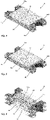
FIG. 1 is a perspective view illustrating a surface mount device chip fuse in accordance with an exemplary embodiment of the present disclosure; -
FIG. 2 is a perspective view illustrating a surface mount device chip fuse in accordance with another exemplary embodiment of the present disclosure; -
FIG. 3 is a perspective view illustrating a surface mount device chip fuse in accordance with another exemplary embodiment of the present disclosure; -
FIG. 4 is a perspective view illustrating a surface mount device chip fuse in accordance with another exemplary embodiment of the present disclosure; -
FIG. 5 is a perspective view illustrating a surface mount device chip fuse in accordance with another exemplary embodiment of the present disclosure; -
FIG. 6 is a perspective view illustrating a surface mount device chip fuse in accordance with another exemplary embodiment of the present disclosure; -
FIG. 7 is a perspective view illustrating a surface mount device chip fuse in accordance with another exemplary embodiment of the present disclosure; -
FIG. 8 is a perspective view illustrating a surface mount device chip fuse in accordance with another exemplary embodiment of the present disclosure. - Exemplary embodiments of a surface mount device (SMD) chip fuse in accordance with the present disclosure will now be described more fully hereinafter with reference to the accompanying drawings. The SMD chip fuse may, however, be embodied in many different forms and should not be construed as being limited to the embodiments set forth herein. Rather, these embodiments are provided so that this disclosure will convey certain exemplary aspects of the SMD chip fuse to those skilled in the art.
- Referring to
FIG. 1 , a perspective view illustrating aSMD chip fuse 10 in accordance with an exemplary embodiment of the present disclosure is shown. TheSMD chip fuse 10 may generally include adielectric substrate 12, electrically conductive first and secondupper terminals lower terminals fusible element 18. Thedielectric substrate 12 may be a substantially planar, rectangular chip formed of a low surface energy, electrically insulating, thermally resistant material. Examples of such materials include, but are not limited to, glass, ceramic, FR-4, perfluoroalkoxy (PFA), ethylene tetrafluoroethylene (ETFE), or polyvinylidene fluoride (PVDF). The longitudinal edges of thedielectric substrate 12 may havesemicircular castellations - The
upper terminals lower terminals dielectric substrate 12, respectively, and may be formed of any suitable electrically conductive material, including, but not limited to, copper, gold, silver, nickel, tin, etc. Theupper terminals dielectric substrate 12 toward one another and may terminate short of the longitudinal center of the top surface to define agap 22 therebetween. Thecastellations terminals lower terminals upper terminal 14a and thelower terminal 16a and between theupper terminal 14b and thelower terminal 16b, respectively. In an alternative embodiment of theSMD chip fuse 10 shown inFIG. 2 , thecastellations longitudinal edges dielectric substrate 12 may be plated or otherwise coated with electrically conductive material to provide electrical connections between theupper terminal 14a and thelower terminal 16a and between theupper terminal 14b and thelower terminal 16b, respectively. In another alternative embodiment of theSMD chip fuse 10 shown inFIG. 3 , electricallyconductive vias dielectric substrate 12, between theupper terminal 14a and thelower terminal 16a and between theupper terminal 14b and thelower terminal 16b, respectively, for providing respective electrical connections therebetween. The present disclosure is not limited in this regard. - Referring back to
FIG. 1 , thefusible element 18 may be formed of a quantity of solder that is disposed on the top surface of thedielectric substrate 12 within thegap 22, bridging theupper terminals fusible element 18 is formed may be selected such that, when the solder is in a melted or semi-melted state, the solder may have an aversion to, or a tendency to draw away from, the surface of thedielectric substrate 12. That is, the material of thedielectric substrate 12 may exhibit a significant "de-wetting" characteristic relative to the solder from which thefusible element 18 is formed. In one example, thedielectric substrate 12 may be formed of PFA and the solder may be SAC305 solder. In another example, thedielectric substrate 12 may be formed of ETFE and the solder may be eutectic solder. In another example, thedielectric substrate 12 may be formed of FR-4, PI (polyimide) and the solder may be a high melt solder (i.e., solder with a melting temperature above 260 degrees Celsius). The present disclosure is not limited in this regard. - During normal operation, the
SMD chip fuse 10 may be connected in a circuit (e.g., thelower terminals lower terminals upper terminals fusible element 18. Upon the occurrence of an overcurrent condition, wherein current flowing through theSMD chip fuse 10 exceeds a current rating of theSMD chip fuse 10, thefusible element 18 may melt or otherwise separate. The current flowing through theSMD chip fuse 10 is thereby arrested to prevent or mitigate damage to connected and surrounding circuit components. - Additionally, owning to the low surface energy and aversive, "de-wetting" characteristic of the
dielectric substrate 12 relative to the melted or semi-melted solder of the fusible element 18 (described above), the separated portions of thefusible element 18 may draw away from one another and away from the surface of thedielectric substrate 12 and may accumulate on the confronting edges/portions of theupper terminals SMD chip fuse 10 in response to an overcurrent condition. Electrical arcing between the separated portions of thefusible element 18 is thereby prevented or mitigated. - Referring to
FIG. 4 , an alternative embodiment of theSMD chip fuse 10 is contemplated in which thefusible element 18 and adjacent portions of theupper terminals dielectric passivation layer 26 for shielding thefusible element 18 from external contaminants and preventing short-circuiting with external circuit components. Thepassivation layer 26 may be formed of epoxy, polyimide, glass, ceramic, or other material that may exhibit a "de-wetting" characteristic relative to the solder from which thefusible element 18 is formed. Thus, when thefusible element 18 melts during an overcurrent condition in theSMD chip fuse 10, the aversive, "de-wetting" characteristic of thepassivation layer 26 relative to the melted or semi-melted solder of thefusible element 18 may repel the separated portions of thefusible element 18 to further assist in galvanic separation therebetween. - Referring to
FIG. 5 , another alternative embodiment of theSMD chip fuse 10 is provided wherein top surfaces of the confronting portions of theupper terminals collection pads 31a, 31b formed of flux or a wetting agent that exhibits a significant affinity or "wetting" characteristic relative to the solder from which thefusible element 18 is formed. Examples of such materials include, but are not limited to, flux compounds made of rosin and/or polyglycol ether. Thus, when thefusible element 18 melts during an overcurrent condition in theSMD chip fuse 10, the melted, separated portions of thefusible element 18 may be drawn to, and may accumulate on, thecollection pads 31a, 31b to further assist in galvanic separation between theupper terminals - Referring to
FIG. 6 , another alternative embodiment of theSMD chip fuse 10 is provided that includes a "non-contact"cover 30 disposed on thefusible element 18 and adjacent portions of theupper terminals fusible element 18 from external contaminants and preventing short-circuiting with external circuit components. Thecover 30 may be substantially identical to the dielectric substrate 12 (e.g., formed from the same material and having the same size and shape as the dielectric substrate 12), but may include acavity 32 formed in a bottom surface thereof. When thecover 30 is stacked atop thedielectric substrate 12 as shown, thefusible element 18 and adjacent portions of theupper terminals cavity 32. - Referring to
FIG. 7 , another alternative embodiment of theSMD chip fuse 10 is provided that includes electrically isolatedmetal pads dielectric substrate 12 and extending into thegap 22, below thefusible element 18. When thefusible element 18 melts during an overcurrent condition in theSMD chip fuse 10, themetal pads fusible element 18 to clear thegap 22 and provide galvanic separation between theupper terminals metal pads - Referring to
FIG. 8 , another alternative embodiment of theSMD chip fuse 10 is provided that includes a pocket ortrench 36 formed in thedielectric substrate 12 below thefusible element 18. When thefusible element 18 melts during an overcurrent condition in theSMD chip fuse 10, thetrench 36 may provide a space for collecting the melted solder of thefusible element 18 to clear thegap 22 and provide galvanic separation between theupper terminals trench 36 may thus facilitate a high fuse rating and low electrical resistance in a small fuse package. - As used herein, an element or step recited in the singular and proceeded with the word "a" or "an" should be understood as not excluding plural elements or steps, unless such exclusion is explicitly recited. Furthermore, references to "one embodiment" of the present disclosure are not intended to be interpreted as excluding the existence of additional embodiments that also incorporate the recited features.
- While the present disclosure makes reference to certain embodiments, numerous modifications, alterations and changes to the described embodiments are possible without departing from the sphere and scope of the present disclosure, as defined in the appended claim(s). Accordingly, it is intended that the present disclosure not be limited to the described embodiments, but that it has the full scope defined by the language of the following claims, and equivalents thereof.
Claims (9)
- A surface mount device chip fuse comprising:a dielectric substrate;electrically conductive first and second upper terminals disposed on a top surface of the dielectric substate and defining a gap therebetween;a fusible element formed of solder disposed on the top surface of the dielectric substate, within the gap, bridging the first and second upper terminals; andelectrically conductive first and second lower terminals disposed on a bottom surface of the dielectric substate and electrically connected to the first and second upper terminals, respectively;wherein a material of the dielectric substrate exhibits a de-wetting characteristic relative to the solder from which the fusible element is formed.
- The surface mount device chip fuse of claim 1, wherein edges of the dielectric substrate include electrically conductive material disposed thereon for providing electrical connections between the first upper terminal and the first lower terminal and between the second upper terminal and the second lower terminal.
- The surface mount device chip fuse of claim 2, wherein edges of the dielectric substrate are castellated.
- The surface mount device chip fuse of claim 1, further comprising electrically conductive vias extending through the dielectric substrate and providing electrical connections between the first upper terminal and the first lower terminal and between the second upper terminal and the second lower terminal.
- The surface mount device chip fuse of claim 1, further comprising a passivation layer disposed on the fusible element and adjacent portions of the first and second upper terminals.
- The surface mount device chip fuse of claim 1, further comprising collection pads disposed on confronting portions of the first and second upper terminals, the collection pads formed of a wetting agent that exhibits a significant wetting characteristic relative to the solder from which the fusible element is formed.
- The surface mount device chip fuse of claim 1, further comprising a non-contact cover disposed on the top surface of the dielectric substrate, the non-contact cover bring formed of a dielectric material and having a cavity formed in a bottom surface thereof, the fusible element being disposed within the cavity.
- The surface mount device chip fuse of claim 1, further comprising electrically isolated metal pads disposed on the top surface of the dielectric substrate and extending into the gap, below the fusible element.
- The surface mount device chip fuse of claim 1, further comprising a trench formed in the top surface of the dielectric substrate, below the fusible element.
Applications Claiming Priority (1)
| Application Number | Priority Date | Filing Date | Title |
|---|---|---|---|
| US17/395,749 US11437212B1 (en) | 2021-08-06 | 2021-08-06 | Surface mount fuse with solder link and de-wetting substrate |
Publications (2)
| Publication Number | Publication Date |
|---|---|
| EP4148763A2 true EP4148763A2 (en) | 2023-03-15 |
| EP4148763A3 EP4148763A3 (en) | 2023-05-03 |
Family
ID=82608458
Family Applications (1)
| Application Number | Title | Priority Date | Filing Date |
|---|---|---|---|
| EP22185051.4A Pending EP4148763A3 (en) | 2021-08-06 | 2022-07-14 | Surface mount fuse with solder link and de-wetting substrate |
Country Status (6)
| Country | Link |
|---|---|
| US (1) | US11437212B1 (en) |
| EP (1) | EP4148763A3 (en) |
| JP (1) | JP7848433B2 (en) |
| KR (1) | KR20230022131A (en) |
| CN (1) | CN115705983A (en) |
| TW (1) | TW202315042A (en) |
Families Citing this family (2)
| Publication number | Priority date | Publication date | Assignee | Title |
|---|---|---|---|---|
| JP1701718S (en) * | 2021-01-18 | 2021-12-06 | ||
| JP1716066S (en) * | 2021-09-01 | 2022-05-27 | fuse |
Family Cites Families (18)
| Publication number | Priority date | Publication date | Assignee | Title |
|---|---|---|---|---|
| US4608548A (en) * | 1985-01-04 | 1986-08-26 | Littelfuse, Inc. | Miniature fuse |
| US5726621A (en) * | 1994-09-12 | 1998-03-10 | Cooper Industries, Inc. | Ceramic chip fuses with multiple current carrying elements and a method for making the same |
| JP3754724B2 (en) * | 1995-06-30 | 2006-03-15 | 内橋エステック株式会社 | Flat temperature fuse |
| US5777540A (en) * | 1996-01-29 | 1998-07-07 | Cts Corporation | Encapsulated fuse having a conductive polymer and non-cured deoxidant |
| JPH11213852A (en) * | 1998-01-28 | 1999-08-06 | Nec Kansai Ltd | Current fuse |
| JP4207686B2 (en) * | 2003-07-01 | 2009-01-14 | パナソニック株式会社 | Fuse, battery pack and fuse manufacturing method using the same |
| DE112006002655T5 (en) * | 2005-10-03 | 2008-08-14 | Littelfuse, Inc., Des Plaines | Fuse with cavity forming housing |
| TWI323906B (en) * | 2007-02-14 | 2010-04-21 | Besdon Technology Corp | Chip-type fuse and method of manufacturing the same |
| JP5489777B2 (en) * | 2010-02-25 | 2014-05-14 | 京セラ株式会社 | Resistance thermal fuse package and resistance thermal fuse |
| JP2014022050A (en) * | 2012-07-12 | 2014-02-03 | Dexerials Corp | Protection element |
| US20140266565A1 (en) * | 2013-03-14 | 2014-09-18 | Littelfuse, Inc. | Laminated electrical fuse |
| US20150009007A1 (en) * | 2013-03-14 | 2015-01-08 | Littelfuse, Inc. | Laminated electrical fuse |
| US10566164B2 (en) * | 2017-04-27 | 2020-02-18 | Manufacturing Networks Incorporated (MNI) | Temperature-triggered fuse device and method of production thereof |
| US11729906B2 (en) * | 2018-12-12 | 2023-08-15 | Eaton Intelligent Power Limited | Printed circuit board with integrated fusing and arc suppression |
| JP7433783B2 (en) * | 2019-06-19 | 2024-02-20 | デクセリアルズ株式会社 | Fuse elements, fuse elements and protection elements |
| JP7433811B2 (en) * | 2019-08-23 | 2024-02-20 | デクセリアルズ株式会社 | Fuse elements, fuse elements and protection elements |
| WO2021101800A1 (en) * | 2019-11-21 | 2021-05-27 | Littelfuse, Inc. | Circuit protection device with ptc device and backup fuse |
| KR102095225B1 (en) * | 2019-12-02 | 2020-03-31 | 장병철 | Chip type fuse using hybrid intergrated circuit technology |
-
2021
- 2021-08-06 US US17/395,749 patent/US11437212B1/en active Active
-
2022
- 2022-07-14 EP EP22185051.4A patent/EP4148763A3/en active Pending
- 2022-07-14 JP JP2022112833A patent/JP7848433B2/en active Active
- 2022-08-01 TW TW111128816A patent/TW202315042A/en unknown
- 2022-08-05 CN CN202210937981.7A patent/CN115705983A/en active Pending
- 2022-08-05 KR KR1020220097667A patent/KR20230022131A/en active Pending
Also Published As
| Publication number | Publication date |
|---|---|
| TW202315042A (en) | 2023-04-01 |
| EP4148763A3 (en) | 2023-05-03 |
| US11437212B1 (en) | 2022-09-06 |
| KR20230022131A (en) | 2023-02-14 |
| CN115705983A (en) | 2023-02-17 |
| JP7848433B2 (en) | 2026-04-21 |
| JP2023024303A (en) | 2023-02-16 |
Similar Documents
| Publication | Publication Date | Title |
|---|---|---|
| TWI398894B (en) | Protection element | |
| US20200176210A1 (en) | Fuse element and fuse device | |
| US8767368B2 (en) | Protective element and method for producing the same | |
| US11145480B2 (en) | Fuse device | |
| US12288660B2 (en) | Protective element | |
| CN113711328B (en) | Protective components and battery packs | |
| EP4062439B1 (en) | Circuit protection device with ptc device and backup fuse | |
| US11437212B1 (en) | Surface mount fuse with solder link and de-wetting substrate | |
| CN106663574A (en) | Chip fuse and fuse element | |
| WO2018159283A1 (en) | Fuse element | |
| TW201805984A (en) | Protection element | |
| US20250079104A1 (en) | Protection device | |
| WO2019026904A1 (en) | Protection element | |
| CN115428112A (en) | Protection element and battery pack | |
| US10446345B2 (en) | Reflowable thermal fuse | |
| US10895609B2 (en) | Circuit protection device with PTC element and secondary fuse | |
| US11501942B2 (en) | PTC device with integrated fuses for high current operation | |
| US20250201505A1 (en) | Chip-type fuse | |
| US20250157774A1 (en) | Chip fuse with floating leads | |
| JP2025130833A (en) | Protection Elements |
Legal Events
| Date | Code | Title | Description |
|---|---|---|---|
| PUAI | Public reference made under article 153(3) epc to a published international application that has entered the european phase |
Free format text: ORIGINAL CODE: 0009012 |
|
| STAA | Information on the status of an ep patent application or granted ep patent |
Free format text: STATUS: THE APPLICATION HAS BEEN PUBLISHED |
|
| AK | Designated contracting states |
Kind code of ref document: A2 Designated state(s): AL AT BE BG CH CY CZ DE DK EE ES FI FR GB GR HR HU IE IS IT LI LT LU LV MC MK MT NL NO PL PT RO RS SE SI SK SM TR |
|
| PUAL | Search report despatched |
Free format text: ORIGINAL CODE: 0009013 |
|
| AK | Designated contracting states |
Kind code of ref document: A3 Designated state(s): AL AT BE BG CH CY CZ DE DK EE ES FI FR GB GR HR HU IE IS IT LI LT LU LV MC MK MT NL NO PL PT RO RS SE SI SK SM TR |
|
| RIC1 | Information provided on ipc code assigned before grant |
Ipc: H01H 69/02 20060101ALI20230328BHEP Ipc: H01H 85/041 20060101AFI20230328BHEP |
|
| STAA | Information on the status of an ep patent application or granted ep patent |
Free format text: STATUS: REQUEST FOR EXAMINATION WAS MADE |
|
| 17P | Request for examination filed |
Effective date: 20231031 |
|
| RBV | Designated contracting states (corrected) |
Designated state(s): AL AT BE BG CH CY CZ DE DK EE ES FI FR GB GR HR HU IE IS IT LI LT LU LV MC MK MT NL NO PL PT RO RS SE SI SK SM TR |
|
| STAA | Information on the status of an ep patent application or granted ep patent |
Free format text: STATUS: EXAMINATION IS IN PROGRESS |
|
| 17Q | First examination report despatched |
Effective date: 20240312 |