EP4148531A1 - Clock configuration system and method - Google Patents
Clock configuration system and method Download PDFInfo
- Publication number
- EP4148531A1 EP4148531A1 EP21828796.9A EP21828796A EP4148531A1 EP 4148531 A1 EP4148531 A1 EP 4148531A1 EP 21828796 A EP21828796 A EP 21828796A EP 4148531 A1 EP4148531 A1 EP 4148531A1
- Authority
- EP
- European Patent Office
- Prior art keywords
- receive
- transmit
- data
- unit
- clock frequency
- Prior art date
- Legal status (The legal status is an assumption and is not a legal conclusion. Google has not performed a legal analysis and makes no representation as to the accuracy of the status listed.)
- Granted
Links
Images


Classifications
-
- G—PHYSICS
- G06—COMPUTING OR CALCULATING; COUNTING
- G06F—ELECTRIC DIGITAL DATA PROCESSING
- G06F1/00—Details not covered by groups G06F3/00 - G06F13/00 and G06F21/00
- G06F1/04—Generating or distributing clock signals or signals derived directly therefrom
-
- G—PHYSICS
- G06—COMPUTING OR CALCULATING; COUNTING
- G06F—ELECTRIC DIGITAL DATA PROCESSING
- G06F1/00—Details not covered by groups G06F3/00 - G06F13/00 and G06F21/00
- G06F1/04—Generating or distributing clock signals or signals derived directly therefrom
- G06F1/08—Clock generators with changeable or programmable clock frequency
Definitions
- Embodiments of the present application relate to the field of communication, and in particular, to a clock configuration system and method.
- a clock configuration system which includes: a clock generation circuit, and a communication module includes a configuration unit, a clock management unit, and a communication circuit; the clock generation circuit is connected to the clock management unit in the communication module; the clock management unit is connected to the communication circuit; and the communication circuit is connected to the configuration unit; the clock generation circuit is configured to provide a reference clock to the communication module; the configuration unit is configured to configure a line rate and a data bit width for data transmission in the communication circuit, determine a clock frequency division coefficient according to the line rate and the data bit width, and set the clock frequency division coefficient into the clock management unit; and the clock management unit is configured to determine an operating clock frequency according to the reference clock and the clock frequency division coefficient, and provide the operating clock frequency to the communication circuit.
- a clock configuration method is provided, which is performed by the clock configuration system according to an embodiment of the present application.
- the method includes: receiving a reference clock, and acquiring a configured line rate and a configured data bit width for data transmission; determining a clock frequency division coefficient according to the line rate and the data bit width; determining an operating clock frequency according to the clock frequency division coefficient and the reference clock; and providing the operating clock frequency to the communication module.
- module means, a suffix such as “module”, “component”, or “unit” used for representing an element is used only for describing the present application, and does not have any particular meanings. Therefore, “module”, “component” and “unit” are exchangeable.
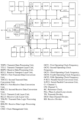
- FIG. 1 depicts a schematic diagram of a clock configuration system according to an embodiment of the present application.
- the system includes: a clock generation circuit 10, a communication module 20, and an AD/DA circuit 30.
- the communication module 20 includes a configuration unit 21, a clock management unit 22, and a communication circuit 23.
- the clock generation circuit 10 is connected to the clock management unit 22 in the communication module 20.
- the clock management unit 22 is connected to the communication circuit 23.
- the communication circuit 23 is connected to the configuration unit 21.
- the clock generation circuit 10 is configured to provide a reference clock to the communication module 20 and the AD/DA circuit 30.
- the configuration unit 21 is configured to configure a line rate and a data bit width of data transmission in the communication circuit 23, determine a clock frequency division coefficient according to the line rate and the data bit width, and configure the clock frequency division coefficient in the clock management unit 22.
- the clock management unit 22 is configured to determine an operating clock frequency according to the reference clock and the clock frequency division coefficient, and provide the operating clock frequency to the communication circuit 23.
- the configuration unit can be understood as a general command center of the system, and configure, according to different application scenarios, various units in a certain order to schedule the operation of the system.
- a look-up table may be pre-generated for configurations of various scenarios, and corresponding configuration information in the table is selected for configuration according to different scenarios. For example, it is assumed that, during scenario switching, first configuration information in the table is selected for Scenario 1, and second configuration information in the table is selected when Scenario 2 is switched to.
- the clock configuration system in the embodiment may be applied to JESD204B/C protocol different-rate clock configuration.
- the clock management unit includes a Phase Locked Loop (PLL) circuit, a transmit divider, and a data channel divider.
- the communication circuit includes a transmit data processing unit, a transmit transport layer unit, a plurality of transmit channels, and a plurality of parallel-serial conversion units, where the transmit channels are in one-to-one correspondence to the parallel-serial conversion units.
- the PLL circuit is connected to the clock generation circuit, the transmit divider, and the data channel divider, respectively.
- the transmit divider is connected to the transmit data processing unit and the transmit transport layer unit, respectively.
- the data channel divider is connected to the plurality of transmit channels. Each transmit channel is connected to a corresponding parallel-serial conversion unit.
- the configuration unit is configured to configure line rates and data bit widths for the transmit channels, determine a first frequency division coefficient according to a total line rate and a total data bit width of the transmit channels, and configure the first frequency division coefficient in the transmit divider.
- the configuration unit is further configured to determine a second frequency division coefficient, and set the second frequency division coefficient into the data channel divider.
- the PLL circuit is configured to transmit the reference clock to the transmit divider and the data channel divider.
- the transmit divider is configured to determine a first operating clock frequency according to the reference clock and the first frequency division coefficient, and provide the first operating clock frequency to the transmit data processing unit and the transmit transport layer unit.
- the data channel divider is configured to determine a second operating clock frequency according to the reference clock and the second frequency division coefficient, and provide the second operating clock frequency to the plurality of transmit channels.
- the plurality of parallel-serial conversion units are each connected to the clock generation circuit and configured to receive the reference clock, and generate, according to the reference clock, a third operating clock frequency required by the parallel-serial conversion units.
- the PLL circuit is configured to adjust the reference clock and transmit the adjusted reference clock to the transmit divider, the data channel divider, and the receive divider.
- the process of adjustment may be a process of frequency spreading of the reference clock.
- the frequency spreading may be understood as increasing the reference clock by an integral multiple. For example, in case that the reference clock is at 150 Hz, the reference clock is at 450 Hz after increasing by 3 times.
- the parallel-serial conversion unit is further configured to convert parallel transmit data to serial transmit data. If N parallel-serial conversion units are present, the clock generation circuit provides N reference clocks.
- the first frequency division coefficient may be determined according to the total line rate and the total data bit width of the transmit channels by: acquiring a first ratio of the total line rate to the total data bit width of the transmit channels; and determining the first frequency division coefficient according to the first ratio and the reference clock.
- the first ratio is a first operating clock frequency.
- the line rate configured for each transmit channel is R1(i) and the configured data bit width is Wl(i)
- the first frequency division coefficient is determined according to the calculated first clock frequency and the adjusted reference clock, and is configured in the transmit divider, so that the transmit divider generates the first operating clock frequency according to the first frequency division coefficient and the adjusted reference clock.
- the first frequency division coefficient may be a ratio of the first clock frequency to the adjusted reference clock.
- the system further includes: a plurality of first transmit data conversion units and a plurality of second transmit data conversion units.
- the first transmit data conversion units and the second transmit data conversion units are in one-to-one correspondence to the transmit channels.
- Each first transmit data conversion unit is connected between the transmit transport layer unit and a respective one of the transmit channels.
- Each second transmit data conversion unit is connected between a respective one of the transmit channels and a respective one of the parallel-serial conversion units.
- Each first transmit data conversion unit has a write end connected to the transmit divider and configured to receive the first operating clock frequency transmitted by the transmit divider.
- Each first transmit data conversion units has a read end connected to the data channel divider and configured to receive the second operating clock frequency transmitted by the data channel divider.
- Each first transmit data conversion unit is configured to convert an operating clock frequency of transmit data from the first operating clock frequency into the second operating clock frequency.
- Each second transmit data conversion unit has a write end connected to the data channel divider and configured to receive the second operating clock frequency transmitted by the data channel divider.
- Each second transmit data conversion unit has a read end connected to a parallel-serial conversion unit and configured to receive the third operating clock frequency transmitted by the parallel-serial conversion unit.
- Each second transmit data conversion unit is configured to convert a bit width of the transmit data, and/or convert the operating clock frequency of the transmit data from the second operating clock frequency into the third operating clock frequency.
- the transmit channel includes: a transmit link layer unit and a transmit data logic processing unit.
- the transmit link layer unit is connected between the first transmit data conversion unit and the transmit data logic processing unit.
- the transmit data logic processing unit is connected between the transmit link layer unit and the second transmit data conversion unit.
- the data channel divider is configured to provide the second operating clock frequency to the transmit link layer unit and the transmit data logic processing unit.
- the transmit link layer unit is configured to encode the transmit data.
- the transmit data logic processing unit is configured to frame and scramble the encoded transmit data.
- the encoding of transmit data may include 8B/10B encoding, 64b/66b encoding or the like.
- the scrambling process may involve: performing a logical operation (such as XOR operation) on a pseudo-random sequence generated by a pseudo-random code generator, and the transmit data, to change features of the transmit data, so as to change the transmit data into an unpredictable data flow.
- the framing may be performed in a manner such that a head and a tail are added to the front and the back of a piece of data to form a frame.
- the clock management unit further includes a receive divider.
- the communication circuit includes a receive data processing unit, a receive transport layer unit, a plurality of receive channels, and a plurality of serial-parallel conversion units.
- the receive channels are in one-to-one correspondence to the serial-parallel conversion units.
- the receive divider is connected to the PLL circuit, the receive data processing unit, and the receive transport layer unit.
- the data channel divider is connected to the plurality of receive channels.
- a receive channel is connected to a respective one of the serial-parallel conversion units.
- the configuration unit is configured to configure line rates and data bit widths of the receive channels, determine a third frequency division coefficient according to a total line rate and a total data bit width of the receive channels, and set the third frequency division coefficient into the receive divider.
- the PLL circuit is configured to transmit the reference clock to the receive divider.
- the receive divider is configured to determine a fourth operating clock frequency according to the reference clock and the third frequency division coefficient, and provide the fourth operating clock frequency to the receive data processing unit and the receive transport layer unit.
- the data channel divider is further configured to provide the second operating clock frequency to the plurality of transmit channels.
- the plurality of serial-parallel conversion units are connected to the clock generation circuit and configured to receive the reference clock, and generate, according to the reference clock, a fifth operating clock frequency required by the serial-parallel conversion units.
- the third frequency division coefficient may be determined according to the total line rate and the total data bit width of the receive channels by: acquiring a second ratio of the total line rate to the total data bit width of the receive channels; and determining the third frequency division coefficient according to the second ratio and the reference clock.
- the second ratio may be understood as the fourth operating clock frequency.
- the third frequency division coefficient is determined according to the calculated fourth clock frequency and the adjusted reference clock, and is set into the receive divider, so that the receive divider generates the fourth operating clock frequency according to the third frequency division coefficient and the adjusted reference clock.
- the third frequency division coefficient may be a ratio of the fourth operating clock frequency to the adjusted reference clock.
- the second frequency division coefficient may be determined by: acquiring a maximum value of the ratios of the line rates to the data bit widths of each of the transmit channels and/or each of the receive channels; and determining the second frequency division coefficient according to the maximum value and the reference clock.
- the second frequency division coefficient is determined according to the calculated second clock frequency and the adjusted reference clock, and is configured in the data channel divider, so that the data channel divider generates the second operating clock frequency according to the second frequency division coefficient and the adjusted reference clock.
- the above processing has the advantage of ensuring that the line rates of data in the transmit link layer unit, the transmit data logic processing unit, the receive link layer unit, and receive data logic processing unit are greater than the line rates of all channels.
- the second frequency division coefficient may be a ratio of the second clock frequency to the adjusted reference clock.
- the system further includes: a plurality of first receive data conversion units and a plurality of second receive data conversion units.
- the first receive data conversion units and the second receive data conversion units are respectively in one-to-one correspondence to the receive channels.
- Each first receive data conversion unit is connected between the receive transport layer unit and a respective one of the receive channels.
- Each second receive data conversion unit is connected between a respective one of the receive channels and a respective one of the parallel-serial conversion units.
- Each first receive data conversion unit has a read end connected to the receive divider and configured to receive the fourth operating clock frequency transmitted by the receive divider.
- Each first receive data conversion unit has a write end connected to the data channel divider and configured to receive the second operating clock frequency transmitted by the data channel divider.
- Each first receive data conversion unit is configured to convert an operating clock frequency of receive data from the second operating clock frequency into the fourth operating clock frequency.
- Each second receive data conversion unit has a read end connected to the data channel divider and configured to receive the second operating clock frequency transmitted by the data channel divider.
- Each second receive data conversion unit has a write end connected to a respective one of the serial-parallel conversion units and configured to receive the fifth operating clock frequency transmitted by the serial-parallel conversion unit.
- Each second receive data conversion unit is configured to convert a bit width of the receive data, and/or convert the operating clock frequency of the receive data from the fifth operating clock frequency into the second operating clock frequency.
- the receive channel includes: a receive link layer unit and a receive data logic processing unit.
- the receive link layer unit is connected between a first receive data conversion unit and a receive data logic processing unit.
- the receive data logic processing unit is connected between a receive link layer unit and a second receive data conversion unit.
- the data channel divider is configured to provide the second operating clock frequency to the receive link layer unit and the receive data logic processing unit.
- the receive link layer unit is configured to decode the receive data.
- the receive data logic processing unit is configured to deframe and descramble the encoded receive data.
- Descrambling is a reverse process of scrambling, and involves performing the same logical operation on the scrambled receive data by the same pseudo-random code as that of a transmitting end, and restoring data before scrambling.
- the deframing is a reverse process of framing, and involves identifying the start and end of a frame according to head and end tags of the receive data after a data flow is received.
- FIG. 2 depicts a schematic diagram of a clock configuration system according to an embodiment of the present application.
- the clock management unit 22 includes a PLL, a transmit divider, a data channel divider, and a receive divider.
- the communication circuit includes a communication circuit responsible for transmit data and a communication circuit responsible for receive data.
- the communication circuit responsible for transmit data includes: a transmit data processing unit, a transmit transport layer unit, a plurality of transmit channels, and a plurality of parallel-serial conversion units.
- Each transmit channel includes a transmit link layer unit and a transmit data logic processing unit.
- the communication circuit responsible for receive data includes: a receive data processing unit, a receive transport layer unit, a plurality of receive channels, and a plurality of serial-parallel conversion units.
- Each receive channel includes a receive link layer unit and a receive data logic processing unit.
- the transmit channels are in one-to-one correspondence to the parallel-serial conversion units.
- the receive channels are in one-to-one correspondence to the serial-parallel conversion units.
- the transmit divider is configured to provide the first operating clock frequency to the transmit data processing unit and the transmit transport layer unit.
- the data channel divider is configured to provide the second operating clock frequency to the transmit link layer unit, the transmit data logic processing unit, the receive link layer unit, and the receive data logic processing unit.
- the receive divider is configured to provide the fourth operating clock frequency to the receive data processing unit and the receive transport layer unit.
- the PLL circuit is connected to the clock generation circuit, the transmit divider, and the data channel divider, respectively.
- the transmit divider is connected to the transmit data processing unit and the transmit transport layer unit.
- the data channel divider is connected to the plurality of transmit channels. Each transmit channel is connected to a respective one of the parallel-serial conversion units.
- the configuration unit 21 is configured to configure line rates and data bit widths for each of the transmit channels, determine a first frequency division coefficient according to a total line rate and a total data bit width of the transmit channels, and set the first frequency division coefficient into the transmit divider; and the configuration unit is further configured to determine a second frequency division coefficient according to the line rate and data bit width of each of the transmit channels and/or the receive channels, and set the second frequency division coefficient into the data channel divider.
- the transmit divider provides the first operating clock frequency to the transmit data processing unit and the transmit transport layer unit.
- the data channel divider provides the second operating clock frequency to a plurality of transmit channels, that is, to the transmit link layer units and the transmit data logic processing units.
- each of the plurality of parallel-serial conversion units is connected to the clock generation circuit and configured to receive the reference clock, and generate, according to the reference clock, a third operating clock frequency required by the parallel-serial conversion units.
- the system further includes: a plurality of first transmit data conversion units and a plurality of second transmit data conversion units.
- the first transmit data conversion units and the second transmit data conversion units are both in one-to-one correspondence to the transmit channels.
- Each first transmit data conversion unit is connected between the transmit transport layer unit and a respective one of the transmit channels.
- Each second transmit data conversion unit is connected between a respective one of the transmit channels and a respective one of the parallel-serial conversion units.
- Each first transmit data conversion unit is configured to convert a clock domain of the transmit data.
- Each second transmit data conversion unit is configured to convert a bit width and/or a clock domain of the transmit data. Converting the clock domain may be understood as converting an operating clock frequency of the transmit data.
- Each first transmit data conversion unit has a write end connected to the transmit divider and configured to receive the first operating clock frequency transmitted by the transmit divider.
- Each first transmit data conversion unit has a read end connected to the data channel divider and configured to receive the second operating clock frequency transmitted by the data channel divider.
- Each first transmit data conversion unit is configured to convert an operating clock frequency of transmit data from the first operating clock frequency into the second operating clock frequency.
- each first transmit data conversion unit can be understood as the end of the first transmit data conversion unit to which data is inputted, and the read end can be understood as the end of the first transmit data conversion unit from which data is outputted.
- Each second transmit data conversion unit has a write end connected to the data channel divider and configured to receive the second operating clock frequency transmitted by the data channel divider.
- Each second transmit data conversion unit has a read end connected to a parallel-serial conversion unit and configured to receive the third operating clock frequency transmitted by the parallel-serial conversion unit.
- Each second transmit data conversion unis is configured to convert a bit width of the transmit data, and/or convert the operating clock frequency of the transmit data from the second operating clock frequency into the third operating clock frequency.
- each second transmit data conversion unit can be understood as the end of the second transmit data conversion unit to which data is inputted, and the read end can be understood as the end of the second transmit data conversion unit from which data is outputted.
- Each of the first transmit data conversion units and the second transmit data conversion units is implemented as a pingpong-RAM.
- the pingRAM and the pongRAM may each store one frame of data.
- data is written at a line rate of R1(i) at the write end, and data is read at a line rate of f2*W1(i) at the read end.
- data is written at a line rate of f2 ⁇ W1(i) at the write end, and data is read at a line rate of R1(i) at the read end.
- the transmit channel includes: a transmit link layer unit and a transmit data logic processing unit.
- Each transmit link layer unit is connected between a first transmit data conversion unit and a transmit data logic processing unit.
- Each transmit data logic processing unit is connected between a transmit link layer unit and a second transmit data conversion unit.
- the data channel divider is configured to provide the second operating clock frequency to the transmit link layer units and the transmit data logic processing units.
- Each transmit link layer unit is configured to encode the transmit data.
- Each transmit data logic processing unit is configured to frame and scramble the encoded transmit data.
- the encoding of the transmit link layer unit and the framing and scrambling of the transmit data logic processing unit are all configured by the configuration unit.
- the clock management unit further includes a receive divider.
- the communication circuit includes a receive data processing unit, a receive transport layer unit, a plurality of receive channels, and a plurality of serial-parallel conversion units.
- the receive channels are in one-to-one correspondence to the serial-parallel conversion units.
- the receive divider is connected to the PLL circuit, the receive data processing unit, and the receive transport layer unit.
- the data channel divider is connected to the plurality of receive channels. Each receive channel is connected to a respective one of the serial-parallel conversion units.
- the configuration unit 21 is configured to configure line rates and data bit widths of the receive channels, determine a third frequency division coefficient according to a total line rate and a total data bit width of the receive channels, and set the third frequency division coefficient into the receive divider.
- the PLL circuit is configured to transmit the adjusted reference clock to the receive divider.
- the receive divider is configured to provide the fourth operating clock frequency to the receive data processing units and the receive transport layer units.
- the data channel divider is further configured to provide the second operating clock frequency to the plurality of transmit channels.
- each of the plurality of serial-parallel conversion unit is connected to the clock generation circuit and configured to receive the reference clock, and generate, according to the reference clock, a fifth operating clock frequency required by the serial-parallel conversion units.
- Each serial-parallel conversion unit is further configured to convert serial receive data into parallel receive data. If N serial-parallel conversion units present, it is necessary for the clock generation circuit provide N reference clocks.
- the system further includes: a plurality of first receive data conversion units and a plurality of second receive data conversion units.
- the first receive data conversion units and the second receive data conversion units are both in one-to-one correspondence to the receive channels.
- Each first receive data conversion unit is connected between the receive transport layer unit and a respective one of the receive channels.
- Each second receive data conversion unit is connected between a respective one of the receive channels and a respective one of the parallel-serial conversion units.
- each first receive data conversion unit is configured to convert a clock domain of the receive data.
- Each second receive data conversion unit is configured to convert a bit width and/or a clock domain of the received data. Converting the clock domain may be understood as converting an operating clock frequency of the received data.
- each first receive data conversion unit has a read end connected to the receive divider and configured to receive the fourth operating clock frequency transmitted by the receive divider.
- Each first receive data conversion unit has a write end connected to the data channel divider and configured to receive the second operating clock frequency transmitted by the data channel divider.
- Each first receive data conversion unit is configured to convert an operating clock frequency of the received data from the second operating clock frequency into the fourth operating clock frequency.
- each first receive data conversion unit can be understood as the end of the first receive data conversion unit to which data is inputted, and the read end can be understood as the end of the first receive data conversion unit from which data is outputted.
- each second receive data conversion unit has a read end connected to the data channel divider and configured to receive the second operating clock frequency transmitted by the data channel divider.
- Each second receive data conversion unit has a write end connected to a serial-parallel conversion unit and configured to receive the fifth operating clock frequency transmitted by the serial-parallel conversion unit.
- Each second receive data conversion unit is configured to convert a bit width of the received data, and/or convert the operating clock frequency of the received data from the fifth operating clock frequency into the second operating clock frequency.
- each second receive data conversion unit can be understood as the end of the second receive data conversion unit to which data is inputted, and the read end can be understood as the end of the second receive data conversion unit from which data is outputted.
- Each of the first receive data conversion units and the second receive data conversion units is implemented as a pingpong-RAM.
- the pingRAM and the pongRAM may each store one frame of data.
- data is written at a line rate of f2*W2(i) at the write end, and data is read at a line rate of R2(i) at the read end.
- data is written at a line rate of R2(i) at the write end, and data is read at a line rate of f2*W2(i) at the read end.
- each receive channel includes: a receive link layer unit and a receive data logic processing unit.
- Each receive link layer unit is connected between a first receive data conversion unit and a receive data logic processing unit.
- Each receive data logic processing unit is connected between a receive link layer unit and a second receive data conversion unit.
- the data channel divider is configured to provide the second operating clock frequency to the receive link layer units and the receive data logic processing units.
- Each receive link layer unit is configured to decode the received data.
- Each receive data logic processing unit is configured to deframe and descramble the encoded received data.
- the decoding of the receive link layer unit and the deframing and descrambling of the receive data logic processing unit are all configured by the configuration unit.
- the transmit link layer units and the transmit data logic processing units in the plurality of transmit channels and the receive link layer units and the receive data logic processing units in the plurality of receive channels share a single second operating clock frequency, so that the number of clocks will not be increased due to an increase in the number of the transmit channels and the receive channels, simplifying the process of clock configuration.
- a clock generation circuit and a communication module are included.
- the communication module includes a configuration unit, a clock management unit, and a communication circuit.
- the clock generation circuit is configured to provide a reference clock to the communication module.
- the configuration unit is configured to configure a line rate and a data bit width of data transmission in the communication circuit, determine a clock frequency division coefficient according to the line rate and the data bit width, and set the clock frequency division coefficient into the clock management unit.
- the clock management unit is configured to determine an operating clock frequency according to the reference clock and the clock frequency division coefficient, and provide the operating clock frequency to the communication circuit. The operating clock frequency is determined according to the configured line rate and data bit width, so that the complexity of clock configuration in the communication module can be reduced.
- FIG. 3 depicts a flowchart of a clock configuration method according to an embodiment of the present application. As shown in FIG. 3 , the method includes S310 to S340.
- a reference clock is received, and a configured line rate and a configured data bit width for data transmission are acquired.
- a clock frequency division coefficient is determined according to the line rate and the data bit width.
- an operating clock frequency is determined according to the clock frequency division coefficient and the reference clock.
- the operating clock frequency is provided to the communication module.
- a reference clock is received, and a configured line rate and a configured data bit width for data transmission are acquired; a clock frequency division coefficient is determined according to the line rate and the data bit width; an operating clock frequency is determined according to the clock frequency division coefficient and the reference clock; and the operating clock frequency is provided to the communication module.
- the operating clock frequency is determined according to the configured line rate and the configured data bit width, so that the complexity of clock configuration in the communication module can be reduced.
- the system includes a clock generation circuit and a communication module.
- the communication module includes a configuration unit, a clock management unit, and a communication circuit.
- the clock generation circuit is configured to provide a reference clock to the communication module.
- the configuration unit is configured to configure a line rate and a data bit width of data transmission in the communication circuit, determine a clock frequency division coefficient according to the line rate and the data bit width, and set the clock frequency division coefficient into the clock management unit.
- the clock management unit is configured to determine an operating clock frequency according to the reference clock and the clock frequency division coefficient, and provide the operating clock frequency to the communication circuit. The operating clock frequency is determined according to the configured line rate and data bit width.
- the plurality of transmit channels and the plurality of receive channels in the communication circuit share one operating clock frequency, so that the number of clocks will not be increased due to an increase in the number of the transmit channels and the receive channels, thus simplifying the process of clock configuration is simplified, and reducing the complexity of clock configuration in the communication module.
- Embodiments of the present application may be implemented as computer program instructions executed by a data processor of a mobile apparatus, for example, in a processor entity, may be implemented as hardware, or may be implemented as a combination of software and hardware.
- the computer program instructions may be assembly instructions, instruction set architecture (ISA) instructions, machine instructions, machine-related instructions, microcodes, firmware instructions, status setting data, or source or object codes written in any combination of one or more programming languages.
- ISA instruction set architecture
Landscapes
- Engineering & Computer Science (AREA)
- Theoretical Computer Science (AREA)
- Physics & Mathematics (AREA)
- General Engineering & Computer Science (AREA)
- General Physics & Mathematics (AREA)
- Synchronisation In Digital Transmission Systems (AREA)
Abstract
Description
- This application is filed on the basis of the
Chinese patent application No. 202010576988.1 filed on June 22, 2020 - Embodiments of the present application relate to the field of communication, and in particular, to a clock configuration system and method.
- In increasingly complex communication systems, with a rapid increase in the amount of data transmission, various communication protocols support higher and higher rates, and the number of data transmission channels integrated into each communication module is increasing. In a single channel, line rates in transmitting and receiving directions are completely independent. The line rates in respective channels are independent, and sampling frequencies in the transmitting and receiving directions are completely independent. The above features bring the advantages of powerful data processing capability and flexible use. At the same time, due to increasing combinations of AD/DA sampling frequencies and transmission channel line rates, a design scale becomes larger and larger. In the case where a conventional clock design and configuration manner continues to be used, the complexity of the system will be increased, and clock configuration is also increasingly difficult.
- In view of the above, according to an embodiment of the present application, a clock configuration system is provided, which includes: a clock generation circuit, and a communication module includes a configuration unit, a clock management unit, and a communication circuit; the clock generation circuit is connected to the clock management unit in the communication module; the clock management unit is connected to the communication circuit; and the communication circuit is connected to the configuration unit; the clock generation circuit is configured to provide a reference clock to the communication module; the configuration unit is configured to configure a line rate and a data bit width for data transmission in the communication circuit, determine a clock frequency division coefficient according to the line rate and the data bit width, and set the clock frequency division coefficient into the clock management unit; and the clock management unit is configured to determine an operating clock frequency according to the reference clock and the clock frequency division coefficient, and provide the operating clock frequency to the communication circuit.
- According to an embodiment of the present application, a clock configuration method is provided, which is performed by the clock configuration system according to an embodiment of the present application. The method includes: receiving a reference clock, and acquiring a configured line rate and a configured data bit width for data transmission; determining a clock frequency division coefficient according to the line rate and the data bit width; determining an operating clock frequency according to the clock frequency division coefficient and the reference clock; and providing the operating clock frequency to the communication module.
-
-
FIG. 1 depicts a schematic diagram of a clock configuration system according to an embodiment of the present application; -
FIG. 2 depicts a schematic diagram of a clock configuration system according to an embodiment of the present application; and -
FIG. 3 depicts a flowchart of a clock configuration method according to an embodiment of the present application. - Objects, technical schemes and advantages of the present application will be clearer from a detailed description of embodiments of the present application in conjunction with the drawings. It is to be noted that if not in collision, the embodiments in the present application and features in the embodiments may be combined with each other.
- It is to be understood that specific embodiments described herein are intended only to explain and not to limit the present application.
- In subsequent descriptions, a suffix such as "module", "component", or "unit" used for representing an element is used only for describing the present application, and does not have any particular meanings. Therefore, "module", "component" and "unit" are exchangeable.
-
FIG. 1 depicts a schematic diagram of a clock configuration system according to an embodiment of the present application. As shown inFIG. 1 , the system includes: aclock generation circuit 10, acommunication module 20, and an AD/DA circuit 30. Thecommunication module 20 includes aconfiguration unit 21, aclock management unit 22, and acommunication circuit 23. - The
clock generation circuit 10 is connected to theclock management unit 22 in thecommunication module 20. Theclock management unit 22 is connected to thecommunication circuit 23. Thecommunication circuit 23 is connected to theconfiguration unit 21. - The
clock generation circuit 10 is configured to provide a reference clock to thecommunication module 20 and the AD/DA circuit 30. Theconfiguration unit 21 is configured to configure a line rate and a data bit width of data transmission in thecommunication circuit 23, determine a clock frequency division coefficient according to the line rate and the data bit width, and configure the clock frequency division coefficient in theclock management unit 22. Theclock management unit 22 is configured to determine an operating clock frequency according to the reference clock and the clock frequency division coefficient, and provide the operating clock frequency to thecommunication circuit 23. - The configuration unit can be understood as a general command center of the system, and configure, according to different application scenarios, various units in a certain order to schedule the operation of the system. A look-up table may be pre-generated for configurations of various scenarios, and corresponding configuration information in the table is selected for configuration according to different scenarios. For example, it is assumed that, during scenario switching, first configuration information in the table is selected for Scenario 1, and second configuration information in the table is selected when Scenario 2 is switched to.
- The clock configuration system in the embodiment may be applied to JESD204B/C protocol different-rate clock configuration.
- In an embodiment, the clock management unit includes a Phase Locked Loop (PLL) circuit, a transmit divider, and a data channel divider. The communication circuit includes a transmit data processing unit, a transmit transport layer unit, a plurality of transmit channels, and a plurality of parallel-serial conversion units, where the transmit channels are in one-to-one correspondence to the parallel-serial conversion units. The PLL circuit is connected to the clock generation circuit, the transmit divider, and the data channel divider, respectively. The transmit divider is connected to the transmit data processing unit and the transmit transport layer unit, respectively. The data channel divider is connected to the plurality of transmit channels. Each transmit channel is connected to a corresponding parallel-serial conversion unit. The configuration unit is configured to configure line rates and data bit widths for the transmit channels, determine a first frequency division coefficient according to a total line rate and a total data bit width of the transmit channels, and configure the first frequency division coefficient in the transmit divider. The configuration unit is further configured to determine a second frequency division coefficient, and set the second frequency division coefficient into the data channel divider. The PLL circuit is configured to transmit the reference clock to the transmit divider and the data channel divider. The transmit divider is configured to determine a first operating clock frequency according to the reference clock and the first frequency division coefficient, and provide the first operating clock frequency to the transmit data processing unit and the transmit transport layer unit. The data channel divider is configured to determine a second operating clock frequency according to the reference clock and the second frequency division coefficient, and provide the second operating clock frequency to the plurality of transmit channels. The plurality of parallel-serial conversion units are each connected to the clock generation circuit and configured to receive the reference clock, and generate, according to the reference clock, a third operating clock frequency required by the parallel-serial conversion units.
- The PLL circuit is configured to adjust the reference clock and transmit the adjusted reference clock to the transmit divider, the data channel divider, and the receive divider. The process of adjustment may be a process of frequency spreading of the reference clock. The frequency spreading may be understood as increasing the reference clock by an integral multiple. For example, in case that the reference clock is at 150 Hz, the reference clock is at 450 Hz after increasing by 3 times.
- The parallel-serial conversion unit is further configured to convert parallel transmit data to serial transmit data. If N parallel-serial conversion units are present, the clock generation circuit provides N reference clocks.
- In an embodiment, the first frequency division coefficient may be determined according to the total line rate and the total data bit width of the transmit channels by: acquiring a first ratio of the total line rate to the total data bit width of the transmit channels; and determining the first frequency division coefficient according to the first ratio and the reference clock.
- In particular, the first ratio is a first operating clock frequency. Provided that the line rate configured for each transmit channel is R1(i) and the configured data bit width is Wl(i), then the determined first operating clock frequency is

- In an embodiment, the system further includes: a plurality of first transmit data conversion units and a plurality of second transmit data conversion units. The first transmit data conversion units and the second transmit data conversion units are in one-to-one correspondence to the transmit channels. Each first transmit data conversion unit is connected between the transmit transport layer unit and a respective one of the transmit channels. Each second transmit data conversion unit is connected between a respective one of the transmit channels and a respective one of the parallel-serial conversion units.
- Each first transmit data conversion unit has a write end connected to the transmit divider and configured to receive the first operating clock frequency transmitted by the transmit divider. Each first transmit data conversion units has a read end connected to the data channel divider and configured to receive the second operating clock frequency transmitted by the data channel divider. Each first transmit data conversion unit is configured to convert an operating clock frequency of transmit data from the first operating clock frequency into the second operating clock frequency.
- Each second transmit data conversion unit has a write end connected to the data channel divider and configured to receive the second operating clock frequency transmitted by the data channel divider. Each second transmit data conversion unit has a read end connected to a parallel-serial conversion unit and configured to receive the third operating clock frequency transmitted by the parallel-serial conversion unit. Each second transmit data conversion unit is configured to convert a bit width of the transmit data, and/or convert the operating clock frequency of the transmit data from the second operating clock frequency into the third operating clock frequency.
- In an embodiment, the transmit channel includes: a transmit link layer unit and a transmit data logic processing unit. The transmit link layer unit is connected between the first transmit data conversion unit and the transmit data logic processing unit. The transmit data logic processing unit is connected between the transmit link layer unit and the second transmit data conversion unit. The data channel divider is configured to provide the second operating clock frequency to the transmit link layer unit and the transmit data logic processing unit.
- The transmit link layer unit is configured to encode the transmit data. The transmit data logic processing unit is configured to frame and scramble the encoded transmit data.
- The encoding of transmit data may include 8B/10B encoding, 64b/66b encoding or the like. The scrambling process may involve: performing a logical operation (such as XOR operation) on a pseudo-random sequence generated by a pseudo-random code generator, and the transmit data, to change features of the transmit data, so as to change the transmit data into an unpredictable data flow. The framing may be performed in a manner such that a head and a tail are added to the front and the back of a piece of data to form a frame.
- In an embodiment, the clock management unit further includes a receive divider. The communication circuit includes a receive data processing unit, a receive transport layer unit, a plurality of receive channels, and a plurality of serial-parallel conversion units. The receive channels are in one-to-one correspondence to the serial-parallel conversion units. The receive divider is connected to the PLL circuit, the receive data processing unit, and the receive transport layer unit. The data channel divider is connected to the plurality of receive channels. A receive channel is connected to a respective one of the serial-parallel conversion units.
- The configuration unit is configured to configure line rates and data bit widths of the receive channels, determine a third frequency division coefficient according to a total line rate and a total data bit width of the receive channels, and set the third frequency division coefficient into the receive divider. The PLL circuit is configured to transmit the reference clock to the receive divider.
- The receive divider is configured to determine a fourth operating clock frequency according to the reference clock and the third frequency division coefficient, and provide the fourth operating clock frequency to the receive data processing unit and the receive transport layer unit.
- The data channel divider is further configured to provide the second operating clock frequency to the plurality of transmit channels. The plurality of serial-parallel conversion units are connected to the clock generation circuit and configured to receive the reference clock, and generate, according to the reference clock, a fifth operating clock frequency required by the serial-parallel conversion units.
- The third frequency division coefficient may be determined according to the total line rate and the total data bit width of the receive channels by: acquiring a second ratio of the total line rate to the total data bit width of the receive channels; and determining the third frequency division coefficient according to the second ratio and the reference clock.
- The second ratio may be understood as the fourth operating clock frequency. Assuming that the line rate configured for each receive channel is R2(i) and the configured data bit width is W2(i), the determined fourth operating clock frequency is

- In an embodiment, the second frequency division coefficient may be determined by: acquiring a maximum value of the ratios of the line rates to the data bit widths of each of the transmit channels and/or each of the receive channels; and determining the second frequency division coefficient according to the maximum value and the reference clock.
- The determined second operating clock frequency is

- In an embodiment, the system further includes: a plurality of first receive data conversion units and a plurality of second receive data conversion units. The first receive data conversion units and the second receive data conversion units are respectively in one-to-one correspondence to the receive channels. Each first receive data conversion unit is connected between the receive transport layer unit and a respective one of the receive channels. Each second receive data conversion unit is connected between a respective one of the receive channels and a respective one of the parallel-serial conversion units.
- Each first receive data conversion unit has a read end connected to the receive divider and configured to receive the fourth operating clock frequency transmitted by the receive divider. Each first receive data conversion unit has a write end connected to the data channel divider and configured to receive the second operating clock frequency transmitted by the data channel divider. Each first receive data conversion unit is configured to convert an operating clock frequency of receive data from the second operating clock frequency into the fourth operating clock frequency.
- Each second receive data conversion unit has a read end connected to the data channel divider and configured to receive the second operating clock frequency transmitted by the data channel divider. Each second receive data conversion unit has a write end connected to a respective one of the serial-parallel conversion units and configured to receive the fifth operating clock frequency transmitted by the serial-parallel conversion unit. Each second receive data conversion unit is configured to convert a bit width of the receive data, and/or convert the operating clock frequency of the receive data from the fifth operating clock frequency into the second operating clock frequency.
- In an embodiment, the receive channel includes: a receive link layer unit and a receive data logic processing unit. The receive link layer unit is connected between a first receive data conversion unit and a receive data logic processing unit. The receive data logic processing unit is connected between a receive link layer unit and a second receive data conversion unit. The data channel divider is configured to provide the second operating clock frequency to the receive link layer unit and the receive data logic processing unit.
- The receive link layer unit is configured to decode the receive data. The receive data logic processing unit is configured to deframe and descramble the encoded receive data.
- Descrambling is a reverse process of scrambling, and involves performing the same logical operation on the scrambled receive data by the same pseudo-random code as that of a transmitting end, and restoring data before scrambling. The deframing is a reverse process of framing, and involves identifying the start and end of a frame according to head and end tags of the receive data after a data flow is received.
-
FIG. 2 depicts a schematic diagram of a clock configuration system according to an embodiment of the present application. As a further illustration of the above embodiment, as shown inFIG. 2 , theclock management unit 22 includes a PLL, a transmit divider, a data channel divider, and a receive divider. The communication circuit includes a communication circuit responsible for transmit data and a communication circuit responsible for receive data. The communication circuit responsible for transmit data includes: a transmit data processing unit, a transmit transport layer unit, a plurality of transmit channels, and a plurality of parallel-serial conversion units. Each transmit channel includes a transmit link layer unit and a transmit data logic processing unit. The communication circuit responsible for receive data includes: a receive data processing unit, a receive transport layer unit, a plurality of receive channels, and a plurality of serial-parallel conversion units. Each receive channel includes a receive link layer unit and a receive data logic processing unit. - The transmit channels are in one-to-one correspondence to the parallel-serial conversion units. The receive channels are in one-to-one correspondence to the serial-parallel conversion units.
- In an embodiment, the transmit divider is configured to provide the first operating clock frequency to the transmit data processing unit and the transmit transport layer unit. The data channel divider is configured to provide the second operating clock frequency to the transmit link layer unit, the transmit data logic processing unit, the receive link layer unit, and the receive data logic processing unit. The receive divider is configured to provide the fourth operating clock frequency to the receive data processing unit and the receive transport layer unit.
- In an embodiment, as shown in
FIG. 2 , the PLL circuit is connected to the clock generation circuit, the transmit divider, and the data channel divider, respectively. The transmit divider is connected to the transmit data processing unit and the transmit transport layer unit. The data channel divider is connected to the plurality of transmit channels. Each transmit channel is connected to a respective one of the parallel-serial conversion units. - In an embodiment, the
configuration unit 21 is configured to configure line rates and data bit widths for each of the transmit channels, determine a first frequency division coefficient according to a total line rate and a total data bit width of the transmit channels, and set the first frequency division coefficient into the transmit divider; and the configuration unit is further configured to determine a second frequency division coefficient according to the line rate and data bit width of each of the transmit channels and/or the receive channels, and set the second frequency division coefficient into the data channel divider. - In an embodiment, the transmit divider provides the first operating clock frequency to the transmit data processing unit and the transmit transport layer unit. The data channel divider provides the second operating clock frequency to a plurality of transmit channels, that is, to the transmit link layer units and the transmit data logic processing units.
- In an embodiment, each of the plurality of parallel-serial conversion units is connected to the clock generation circuit and configured to receive the reference clock, and generate, according to the reference clock, a third operating clock frequency required by the parallel-serial conversion units.
- In an embodiment, as shown in
FIG. 2 , the system further includes: a plurality of first transmit data conversion units and a plurality of second transmit data conversion units. The first transmit data conversion units and the second transmit data conversion units are both in one-to-one correspondence to the transmit channels. Each first transmit data conversion unit is connected between the transmit transport layer unit and a respective one of the transmit channels. Each second transmit data conversion unit is connected between a respective one of the transmit channels and a respective one of the parallel-serial conversion units. - Each first transmit data conversion unit is configured to convert a clock domain of the transmit data. Each second transmit data conversion unit is configured to convert a bit width and/or a clock domain of the transmit data. Converting the clock domain may be understood as converting an operating clock frequency of the transmit data.
- Each first transmit data conversion unit has a write end connected to the transmit divider and configured to receive the first operating clock frequency transmitted by the transmit divider. Each first transmit data conversion unit has a read end connected to the data channel divider and configured to receive the second operating clock frequency transmitted by the data channel divider. Each first transmit data conversion unit is configured to convert an operating clock frequency of transmit data from the first operating clock frequency into the second operating clock frequency.
- The write end of each first transmit data conversion unit can be understood as the end of the first transmit data conversion unit to which data is inputted, and the read end can be understood as the end of the first transmit data conversion unit from which data is outputted.
- Each second transmit data conversion unit has a write end connected to the data channel divider and configured to receive the second operating clock frequency transmitted by the data channel divider. Each second transmit data conversion unit has a read end connected to a parallel-serial conversion unit and configured to receive the third operating clock frequency transmitted by the parallel-serial conversion unit. Each second transmit data conversion unis is configured to convert a bit width of the transmit data, and/or convert the operating clock frequency of the transmit data from the second operating clock frequency into the third operating clock frequency.
- The write end of each second transmit data conversion unit can be understood as the end of the second transmit data conversion unit to which data is inputted, and the read end can be understood as the end of the second transmit data conversion unit from which data is outputted.
- Each of the first transmit data conversion units and the second transmit data conversion units is implemented as a pingpong-RAM. The pingRAM and the pongRAM may each store one frame of data. In each first transmit data conversion unit, data is written at a line rate of R1(i) at the write end, and data is read at a line rate of f2*W1(i) at the read end. In each second transmit data conversion unit, data is written at a line rate of f2∗W1(i) at the write end, and data is read at a line rate of R1(i) at the read end.
- In an embodiment, as shown in
FIG. 2 , the transmit channel includes: a transmit link layer unit and a transmit data logic processing unit. Each transmit link layer unit is connected between a first transmit data conversion unit and a transmit data logic processing unit. Each transmit data logic processing unit is connected between a transmit link layer unit and a second transmit data conversion unit. The data channel divider is configured to provide the second operating clock frequency to the transmit link layer units and the transmit data logic processing units. - Each transmit link layer unit is configured to encode the transmit data. Each transmit data logic processing unit is configured to frame and scramble the encoded transmit data. In this embodiment, the encoding of the transmit link layer unit and the framing and scrambling of the transmit data logic processing unit are all configured by the configuration unit.
- In an embodiment, as shown in
FIG. 2 , the clock management unit further includes a receive divider. The communication circuit includes a receive data processing unit, a receive transport layer unit, a plurality of receive channels, and a plurality of serial-parallel conversion units. The receive channels are in one-to-one correspondence to the serial-parallel conversion units. - In an embodiment, as shown in
FIG. 2 , the receive divider is connected to the PLL circuit, the receive data processing unit, and the receive transport layer unit. The data channel divider is connected to the plurality of receive channels. Each receive channel is connected to a respective one of the serial-parallel conversion units. - The
configuration unit 21 is configured to configure line rates and data bit widths of the receive channels, determine a third frequency division coefficient according to a total line rate and a total data bit width of the receive channels, and set the third frequency division coefficient into the receive divider. - The PLL circuit is configured to transmit the adjusted reference clock to the receive divider. The receive divider is configured to provide the fourth operating clock frequency to the receive data processing units and the receive transport layer units.
- In this embodiment, the data channel divider is further configured to provide the second operating clock frequency to the plurality of transmit channels.
- In an embodiment, each of the plurality of serial-parallel conversion unit is connected to the clock generation circuit and configured to receive the reference clock, and generate, according to the reference clock, a fifth operating clock frequency required by the serial-parallel conversion units.
- Each serial-parallel conversion unit is further configured to convert serial receive data into parallel receive data. If N serial-parallel conversion units present, it is necessary for the clock generation circuit provide N reference clocks.
- In an embodiment, the system further includes: a plurality of first receive data conversion units and a plurality of second receive data conversion units. The first receive data conversion units and the second receive data conversion units are both in one-to-one correspondence to the receive channels.
- Each first receive data conversion unit is connected between the receive transport layer unit and a respective one of the receive channels. Each second receive data conversion unit is connected between a respective one of the receive channels and a respective one of the parallel-serial conversion units.
- In this embodiment, each first receive data conversion unit is configured to convert a clock domain of the receive data. Each second receive data conversion unit is configured to convert a bit width and/or a clock domain of the received data. Converting the clock domain may be understood as converting an operating clock frequency of the received data.
- In an embodiment, each first receive data conversion unit has a read end connected to the receive divider and configured to receive the fourth operating clock frequency transmitted by the receive divider. Each first receive data conversion unit has a write end connected to the data channel divider and configured to receive the second operating clock frequency transmitted by the data channel divider. Each first receive data conversion unit is configured to convert an operating clock frequency of the received data from the second operating clock frequency into the fourth operating clock frequency.
- The write end of each first receive data conversion unit can be understood as the end of the first receive data conversion unit to which data is inputted, and the read end can be understood as the end of the first receive data conversion unit from which data is outputted.
- In an embodiment, each second receive data conversion unit has a read end connected to the data channel divider and configured to receive the second operating clock frequency transmitted by the data channel divider. Each second receive data conversion unit has a write end connected to a serial-parallel conversion unit and configured to receive the fifth operating clock frequency transmitted by the serial-parallel conversion unit. Each second receive data conversion unit is configured to convert a bit width of the received data, and/or convert the operating clock frequency of the received data from the fifth operating clock frequency into the second operating clock frequency.
- The write end of each second receive data conversion unit can be understood as the end of the second receive data conversion unit to which data is inputted, and the read end can be understood as the end of the second receive data conversion unit from which data is outputted.
- Each of the first receive data conversion units and the second receive data conversion units is implemented as a pingpong-RAM. The pingRAM and the pongRAM may each store one frame of data. In each first transmit data conversion unit, data is written at a line rate of f2*W2(i) at the write end, and data is read at a line rate of R2(i) at the read end. In each second transmit data conversion unit, data is written at a line rate of R2(i) at the write end, and data is read at a line rate of f2*W2(i) at the read end.
- In an embodiment, each receive channel includes: a receive link layer unit and a receive data logic processing unit. Each receive link layer unit is connected between a first receive data conversion unit and a receive data logic processing unit. Each receive data logic processing unit is connected between a receive link layer unit and a second receive data conversion unit. The data channel divider is configured to provide the second operating clock frequency to the receive link layer units and the receive data logic processing units.
- Each receive link layer unit is configured to decode the received data. Each receive data logic processing unit is configured to deframe and descramble the encoded received data. In this embodiment, the decoding of the receive link layer unit and the deframing and descrambling of the receive data logic processing unit are all configured by the configuration unit.
- In this embodiment, the transmit link layer units and the transmit data logic processing units in the plurality of transmit channels and the receive link layer units and the receive data logic processing units in the plurality of receive channels share a single second operating clock frequency, so that the number of clocks will not be increased due to an increase in the number of the transmit channels and the receive channels, simplifying the process of clock configuration.
- In the technical scheme of this embodiment, a clock generation circuit and a communication module are included. The communication module includes a configuration unit, a clock management unit, and a communication circuit. The clock generation circuit is configured to provide a reference clock to the communication module. The configuration unit is configured to configure a line rate and a data bit width of data transmission in the communication circuit, determine a clock frequency division coefficient according to the line rate and the data bit width, and set the clock frequency division coefficient into the clock management unit. The clock management unit is configured to determine an operating clock frequency according to the reference clock and the clock frequency division coefficient, and provide the operating clock frequency to the communication circuit. The operating clock frequency is determined according to the configured line rate and data bit width, so that the complexity of clock configuration in the communication module can be reduced.
-
FIG. 3 depicts a flowchart of a clock configuration method according to an embodiment of the present application. As shown inFIG. 3 , the method includes S310 to S340. - At S310, a reference clock is received, and a configured line rate and a configured data bit width for data transmission are acquired.
- At S320, a clock frequency division coefficient is determined according to the line rate and the data bit width.
- At S330, an operating clock frequency is determined according to the clock frequency division coefficient and the reference clock.
- At S340, the operating clock frequency is provided to the communication module.
- Please refer to the description in the above embodiments for the procedure of clock configuration, which is not repeated here.
- In this embodiment, a reference clock is received, and a configured line rate and a configured data bit width for data transmission are acquired; a clock frequency division coefficient is determined according to the line rate and the data bit width; an operating clock frequency is determined according to the clock frequency division coefficient and the reference clock; and the operating clock frequency is provided to the communication module. The operating clock frequency is determined according to the configured line rate and the configured data bit width, so that the complexity of clock configuration in the communication module can be reduced.
- Clock configuration system and method are provided in the embodiments of the present application, the system includes a clock generation circuit and a communication module. The communication module includes a configuration unit, a clock management unit, and a communication circuit. The clock generation circuit is configured to provide a reference clock to the communication module. The configuration unit is configured to configure a line rate and a data bit width of data transmission in the communication circuit, determine a clock frequency division coefficient according to the line rate and the data bit width, and set the clock frequency division coefficient into the clock management unit. The clock management unit is configured to determine an operating clock frequency according to the reference clock and the clock frequency division coefficient, and provide the operating clock frequency to the communication circuit. The operating clock frequency is determined according to the configured line rate and data bit width. The plurality of transmit channels and the plurality of receive channels in the communication circuit share one operating clock frequency, so that the number of clocks will not be increased due to an increase in the number of the transmit channels and the receive channels, thus simplifying the process of clock configuration is simplified, and reducing the complexity of clock configuration in the communication module.
- Some embodiments of the present application are described above and which are not intended to limit the protection scope of the present application.
- Embodiments of the present application may be implemented as computer program instructions executed by a data processor of a mobile apparatus, for example, in a processor entity, may be implemented as hardware, or may be implemented as a combination of software and hardware. The computer program instructions may be assembly instructions, instruction set architecture (ISA) instructions, machine instructions, machine-related instructions, microcodes, firmware instructions, status setting data, or source or object codes written in any combination of one or more programming languages.
- A detailed description of example embodiments of the present application has been provided above through demonstrative and non-restrictive examples. However, in consideration of the drawings and claims, various modifications and alternations to the above embodiments are obvious to those skilled in the art, without departing from the scope of the present application. Accordingly, the proper scope of the present application will be defined by the claims.
Claims (13)
- A clock configuration system, comprising: a clock generation circuit, and a communication module comprising a configuration unit, a clock management unit, and a communication circuit; wherein,the clock generation circuit is connected to the clock management unit in the communication module; the clock management unit is connected to the communication circuit, and the communication circuit is connected to the configuration unit;the clock generation circuit is configured to provide a reference clock to the communication module; the configuration unit is configured to configure a line rate and a data bit width for data transmission in the communication circuit, determine a clock frequency division coefficient according to the line rate and the data bit width, and set the clock frequency division coefficient into the clock management unit; andthe clock management unit is configured to determine an operating clock frequency according to the reference clock and the clock frequency division coefficient, and provide the operating clock frequency to the communication circuit.
- The system of claim 1, wherein the clock management unit comprises a Phase Locked Loop, PLL, circuit, a transmit divider, and a data channel divider; the communication circuit comprises a transmit data processing unit, a transmit transport layer unit, a plurality of transmit channels, and a plurality of parallel-serial conversion units; wherein each transmit channel corresponds to a respective one of the parallel-serial conversion units;the PLL circuit is connected to the clock generation circuit, the transmit divider, and the data channel divider; the transmit divider is connected to the transmit data processing unit and the transmit transport layer unit; the data channel divider is connected to each of the plurality of transmit channels, and each transmit channel is connected to a respective one of the parallel-serial conversion units;the configuration unit is configured to configure a line rate and a data bit width for each transmit channel, determine a first frequency division coefficient according to a total line rate and a total data bit width of the transmit channels, and set the first frequency division coefficient into the transmit divider; the configuration unit is further configured to determine a second frequency division coefficient, and set the second frequency division coefficient into the data channel divider;the PLL circuit is configured to transmit the reference clock to the transmit divider and the data channel divider;the transmit divider is configured to determine a first operating clock frequency according to the reference clock and the first frequency division coefficient, and provide the first operating clock frequency to the transmit data processing unit and the transmit transport layer unit;the data channel divider is configured to determine a second operating clock frequency according to the reference clock and the second frequency division coefficient, and provide the second operating clock frequency to each of the plurality of transmit channels; andeach of the plurality of parallel-serial conversion units is connected to the clock generation circuit and is configured to receive the reference clock, and generate, according to the reference clock, a third operating clock frequency for each parallel-serial conversion unit.
- The system of claim 2, wherein determination of the first frequency division coefficient according to the total line rate and the total data bit width of the transmit channels comprises:acquiring a first ratio of the total line rate to the total data bit width of the transmit channels; anddetermining the first frequency division coefficient according to the first ratio and the reference clock.
- The system of claim 2, further comprising: a plurality of first transmit data conversion units and a plurality of second transmit data conversion units, and each first transmit data conversion unit and each second transmit data conversion unit corresponding to a respective one of the transmit channels; wherein,each first transmit data conversion unit is connected between the transmit transport layer unit and a respective one of the transmit channels, and each second transmit data conversion unit is connected between a respective one of the transmit channels and a respective one of the parallel-serial conversion units;each first transmit data conversion unit has, a write end connected to the transmit divider and configured to receive the first operating clock frequency transmitted by the transmit divider, and a read end connected to the data channel divider and configured to receive the second operating clock frequency transmitted by the data channel divider; and each first transmit data conversion unit is configured to convert an operating clock frequency of transmit data from the first operating clock frequency into the second operating clock frequency; andeach second transmit data conversion unit has a write end connected to the data channel divider and configured to receive the second operating clock frequency transmitted by the data channel divider, and a read end connected to a respective one of the parallel-serial conversion units and configured to receive the third operating clock frequency transmitted by the respective one of the parallel-serial conversion units, and each second transmit data conversion unit is configured to convert a bit width of the transmit data, and/or convert an operating clock frequency of the transmit data from the second operating clock frequency into the third operating clock frequency.
- The system of claim 4, wherein each transmit channel comprises a transmit link layer unit and a transmit data logic processing unit;the transmit link layer unit is connected between a respective one of the first transmit data conversion units and a respective one of the transmit data logic processing units; and the transmit data logic processing unit is connected between the transmit link layer unit and a respective one of the second transmit data conversion units; andthe data channel divider is configured to provide the second operating clock frequency to the transmit link layer unit and the transmit data logic processing unit of each transmit channel.
- The system of claim 5, wherein the transmit link layer unit is configured to encode the transmit data, and the transmit data logic processing unit is configured to frame and scramble the encoded transmit data.
- The system of claim 2, wherein the clock management unit further comprises a receive divider; the communication circuit comprises a receive data processing unit, a receive transport layer unit, a plurality of receive channels, and a plurality of serial-parallel conversion units; wherein each receive channel corresponds to a respective one of the serial-parallel conversion units;the receive divider is connected to the PLL circuit, the receive data processing unit, and the receive transport layer unit; the data channel divider is connected to each of the plurality of receive channels; and each receive channel is connected to a respective one of the serial-parallel conversion units;the configuration unit is configured to configure a line rate and a data bit width for each receive channel, determine a third frequency division coefficient according to a total line rate and a total data bit width of the receive channels, and set the third frequency division coefficient into the receive divider;the PLL circuit is configured to transmit the reference clock to the receive divider;the receive divider is configured to determine a fourth operating clock frequency according to the reference clock and the third frequency division coefficient, and provide the fourth operating clock frequency to the receive data processing unit and the receive transport layer unit;the data channel divider is further configured to provide the second operating clock frequency to each of the plurality of transmit channels; andeach of the plurality of serial-parallel conversion units is connected to the clock generation circuit and is configured to receive the reference clock, and generate, according to the reference clock, a fifth operating clock frequency for each serial-parallel conversion unit.
- The system of claim 7, wherein determination of the third frequency division coefficient according to the total line rate and the total data bit width of the receive channels comprises:acquiring a second ratio of the total line rate to the total data bit width of the receive channels; anddetermining the third frequency division coefficient according to the second ratio and the reference clock.
- The system of claim 7, wherein determination of the second frequency division coefficient comprises:acquiring a maximum value of the ratio of the line rate to the data bit width among the transmit channels and/or among the receive channels; anddetermining the second frequency division coefficient according to the maximum value and the reference clock.
- The system of claim 7, further comprising: a plurality of first receive data conversion units and a plurality of second receive data conversion units; and each first receive data conversion unit and each second receive data conversion unit corresponding to a respective one of the receive channels; wherein,each first receive data conversion unit is connected between the receive transport layer unit and a respective one of the receive channels, and each second receive data conversion unit is connected between a respective one of the receive channels and a respective one of the parallel-serial conversion units;each first receive data conversion unit has, a read end connected to the receive divider and configured to receive the fourth operating clock frequency transmitted by the receive divider, and a write end connected to the data channel divider and configured to receive the second operating clock frequency transmitted by the data channel divider; and each first receive data conversion unit is configured to convert an operating clock frequency of receive data from the second operating clock frequency into the fourth operating clock frequency; andeach second receive data conversion unit has, a read end connected to the data channel divider and configured to receive the second operating clock frequency transmitted by the data channel divider, and a write end connected to a respective one of the serial-parallel conversion units and configured to receive the fifth operating clock frequency transmitted by the respective one of the serial-parallel conversion units; and each second receive data conversion unit is configured to convert a bit width of the receive data, and/or convert an operating clock frequency of the receive data from the fifth operating clock frequency into the second operating clock frequency.
- The system of claim 10, wherein each receive channel comprises a receive link layer unit and a receive data logic processing unit;the receive link layer unit is connected between a respective one of the first receive data conversion units and the receive data logic processing unit, and the receive data logic processing unit is connected between the receive link layer unit and a respective one of the second receive data conversion units; andthe data channel divider is configured to provide the second operating clock frequency to the receive link layer unit and the receive data logic processing unit of each receive channel.
- The system of claim 11, wherein the receive link layer unit is configured to decode the receive data; and the receive data logic processing unit is configured to deframe and descramble the encoded receive data.
- A clock generation method, performed by the system of any one of claims 1 to 12, comprising:receiving a reference clock, and acquiring a configured line rate and a configured data bit width for data transmission;determining a clock frequency division coefficient according to the line rate and the data bit width;determining an operating clock frequency according to the clock frequency division coefficient and the reference clock; andproviding the operating clock frequency to the communication module.
Applications Claiming Priority (2)
| Application Number | Priority Date | Filing Date | Title |
|---|---|---|---|
| CN202010576988.1A CN113900477B (en) | 2020-06-22 | 2020-06-22 | A clock configuration system and method |
| PCT/CN2021/095563 WO2021258956A1 (en) | 2020-06-22 | 2021-05-24 | Clock configuration system and method |
Publications (3)
| Publication Number | Publication Date |
|---|---|
| EP4148531A1 true EP4148531A1 (en) | 2023-03-15 |
| EP4148531A4 EP4148531A4 (en) | 2023-11-15 |
| EP4148531B1 EP4148531B1 (en) | 2026-02-25 |
Family
ID=79186556
Family Applications (1)
| Application Number | Title | Priority Date | Filing Date |
|---|---|---|---|
| EP21828796.9A Active EP4148531B1 (en) | 2020-06-22 | 2021-05-24 | Clock configuration system and method |
Country Status (3)
| Country | Link |
|---|---|
| EP (1) | EP4148531B1 (en) |
| CN (1) | CN113900477B (en) |
| WO (1) | WO2021258956A1 (en) |
Families Citing this family (1)
| Publication number | Priority date | Publication date | Assignee | Title |
|---|---|---|---|---|
| CN120597565B (en) * | 2025-08-05 | 2025-11-04 | 桔帧科技(江苏)有限公司 | Label chip and digital baseband clock configuration method thereof |
Family Cites Families (6)
| Publication number | Priority date | Publication date | Assignee | Title |
|---|---|---|---|---|
| CN101446845B (en) * | 2008-12-19 | 2010-06-02 | 锐迪科微电子(上海)有限公司 | Frequency-adjusting device |
| CN205563555U (en) * | 2016-04-07 | 2016-09-07 | 成都华日通讯技术有限公司 | Implementation system of self -defined variable bit wide SPI bus agreement based on FPGA |
| EP3343773B1 (en) * | 2016-12-29 | 2022-06-01 | Nxp B.V. | Chirp generator using a pll |
| CN107315448A (en) * | 2017-06-26 | 2017-11-03 | 北方电子研究院安徽有限公司 | A kind of Clock management architecture design method of low-Power Multicore SoC |
| CN109521834B (en) * | 2018-10-31 | 2021-04-06 | 武汉精立电子技术有限公司 | DP signal generating device and method |
| CN109361381B (en) * | 2018-12-10 | 2024-05-03 | 珠海一微半导体股份有限公司 | PWM generating circuit, processing circuit and chip |
-
2020
- 2020-06-22 CN CN202010576988.1A patent/CN113900477B/en active Active
-
2021
- 2021-05-24 EP EP21828796.9A patent/EP4148531B1/en active Active
- 2021-05-24 WO PCT/CN2021/095563 patent/WO2021258956A1/en not_active Ceased
Also Published As
| Publication number | Publication date |
|---|---|
| CN113900477A (en) | 2022-01-07 |
| WO2021258956A1 (en) | 2021-12-30 |
| CN113900477B (en) | 2026-03-06 |
| EP4148531B1 (en) | 2026-02-25 |
| EP4148531A4 (en) | 2023-11-15 |
Similar Documents
| Publication | Publication Date | Title |
|---|---|---|
| US5258999A (en) | Circuit and method for receiving and transmitting control and status information | |
| US8665856B2 (en) | Data processing apparatus, communication device, and data processing method | |
| RU2701192C2 (en) | Transmission device and method of transmitting an aggregated protocol physical layer data protocol unit | |
| US6618395B1 (en) | Physical coding sub-layer for transmission of data over multi-channel media | |
| JP5203699B2 (en) | Method and apparatus for minimizing co-channel interference | |
| JPH0786982A (en) | Synchronous pn code sequence generation circuit | |
| JPS6126739B2 (en) | ||
| EP4148531B1 (en) | Clock configuration system and method | |
| US8520789B2 (en) | Method and apparatus for implementing pulse synchronization | |
| US5629983A (en) | Parallel transmission through plurality of optical fibers | |
| WO1997028612A1 (en) | Code synchronization in multi-user spread-spectrum systems | |
| US7352301B2 (en) | Method for transmitting a data flow over an optical bus, corresponding system and computer program product | |
| US8824469B2 (en) | Packet communication device for communicating packet to be transferred through packet communication which is time-managed in constant cycle and packet communication method thereof | |
| CN115017084A (en) | Multifunctional serial interface communication device and serial data transmission control method | |
| EP1955470B1 (en) | Synchronized receiver | |
| TW202125486A (en) | Display driving device and display device including the same | |
| US11146292B2 (en) | Data decoding apparatus and method | |
| CN112188446B (en) | Synchronization signal sending method, terminal, device and storage medium | |
| CN113271567B (en) | Information sending and receiving method, device and terminal | |
| CN117910058B (en) | Data processing method and system based on data security protection between FPGA chips | |
| US12082136B2 (en) | Radio communication apparatus and radio communication method | |
| CN111464276A (en) | Signal sending and receiving method and device | |
| JP2019212945A (en) | Wireless transmission device, communication control method, communication control program, and wireless transmission system | |
| EP0535435A2 (en) | A circuit and method for receiving and transmitting control and status information | |
| JP2000354032A (en) | Pseudo-noise series containing pseudo noise series having various lengths and inserted at various positions |
Legal Events
| Date | Code | Title | Description |
|---|---|---|---|
| STAA | Information on the status of an ep patent application or granted ep patent |
Free format text: STATUS: THE INTERNATIONAL PUBLICATION HAS BEEN MADE |
|
| PUAI | Public reference made under article 153(3) epc to a published international application that has entered the european phase |
Free format text: ORIGINAL CODE: 0009012 |
|
| STAA | Information on the status of an ep patent application or granted ep patent |
Free format text: STATUS: REQUEST FOR EXAMINATION WAS MADE |
|
| 17P | Request for examination filed |
Effective date: 20221206 |
|
| AK | Designated contracting states |
Kind code of ref document: A1 Designated state(s): AL AT BE BG CH CY CZ DE DK EE ES FI FR GB GR HR HU IE IS IT LI LT LU LV MC MK MT NL NO PL PT RO RS SE SI SK SM TR |
|
| DAV | Request for validation of the european patent (deleted) | ||
| DAX | Request for extension of the european patent (deleted) | ||
| A4 | Supplementary search report drawn up and despatched |
Effective date: 20231016 |
|
| RIC1 | Information provided on ipc code assigned before grant |
Ipc: G06F 1/08 20060101AFI20231010BHEP |
|
| GRAP | Despatch of communication of intention to grant a patent |
Free format text: ORIGINAL CODE: EPIDOSNIGR1 |
|
| STAA | Information on the status of an ep patent application or granted ep patent |
Free format text: STATUS: GRANT OF PATENT IS INTENDED |
|
| INTG | Intention to grant announced |
Effective date: 20251126 |
|
| GRAS | Grant fee paid |
Free format text: ORIGINAL CODE: EPIDOSNIGR3 |
|
| GRAA | (expected) grant |
Free format text: ORIGINAL CODE: 0009210 |
|
| STAA | Information on the status of an ep patent application or granted ep patent |
Free format text: STATUS: THE PATENT HAS BEEN GRANTED |
|
| AK | Designated contracting states |
Kind code of ref document: B1 Designated state(s): AL AT BE BG CH CY CZ DE DK EE ES FI FR GB GR HR HU IE IS IT LI LT LU LV MC MK MT NL NO PL PT RO RS SE SI SK SM TR |
|
| REG | Reference to a national code |
Ref country code: CH Ref legal event code: F10 Free format text: ST27 STATUS EVENT CODE: U-0-0-F10-F00 (AS PROVIDED BY THE NATIONAL OFFICE) Effective date: 20260225 Ref country code: GB Ref legal event code: FG4D |
|
| REG | Reference to a national code |
Ref country code: DE Ref legal event code: R096 Ref document number: 602021048820 Country of ref document: DE |
|
| REG | Reference to a national code |
Ref country code: IE Ref legal event code: FG4D |
|
| PGFP | Annual fee paid to national office [announced via postgrant information from national office to epo] |
Ref country code: GB Payment date: 20260325 Year of fee payment: 6 |