EP4145137A1 - Testing chip and method for manufacturing same - Google Patents
Testing chip and method for manufacturing same Download PDFInfo
- Publication number
- EP4145137A1 EP4145137A1 EP21797891.5A EP21797891A EP4145137A1 EP 4145137 A1 EP4145137 A1 EP 4145137A1 EP 21797891 A EP21797891 A EP 21797891A EP 4145137 A1 EP4145137 A1 EP 4145137A1
- Authority
- EP
- European Patent Office
- Prior art keywords
- liquid
- layer
- section
- test
- test chip
- Prior art date
- Legal status (The legal status is an assumption and is not a legal conclusion. Google has not performed a legal analysis and makes no representation as to the accuracy of the status listed.)
- Granted
Links
Images





Classifications
-
- B—PERFORMING OPERATIONS; TRANSPORTING
- B01—PHYSICAL OR CHEMICAL PROCESSES OR APPARATUS IN GENERAL
- B01L—CHEMICAL OR PHYSICAL LABORATORY APPARATUS FOR GENERAL USE
- B01L3/00—Containers or dishes for laboratory use, e.g. laboratory glassware; Droppers
- B01L3/50—Containers for the purpose of retaining a material to be analysed, e.g. test tubes
- B01L3/502—Containers for the purpose of retaining a material to be analysed, e.g. test tubes with fluid transport, e.g. in multi-compartment structures
- B01L3/5023—Containers for the purpose of retaining a material to be analysed, e.g. test tubes with fluid transport, e.g. in multi-compartment structures with a sample being transported to, and subsequently stored in an absorbent for analysis
-
- G—PHYSICS
- G01—MEASURING; TESTING
- G01N—INVESTIGATING OR ANALYSING MATERIALS BY DETERMINING THEIR CHEMICAL OR PHYSICAL PROPERTIES
- G01N35/00—Automatic analysis not limited to methods or materials provided for in any single one of groups G01N1/00 - G01N33/00; Handling materials therefor
- G01N35/08—Automatic analysis not limited to methods or materials provided for in any single one of groups G01N1/00 - G01N33/00; Handling materials therefor using a stream of discrete samples flowing along a tube system, e.g. flow injection analysis
-
- B—PERFORMING OPERATIONS; TRANSPORTING
- B01—PHYSICAL OR CHEMICAL PROCESSES OR APPARATUS IN GENERAL
- B01L—CHEMICAL OR PHYSICAL LABORATORY APPARATUS FOR GENERAL USE
- B01L3/00—Containers or dishes for laboratory use, e.g. laboratory glassware; Droppers
- B01L3/50—Containers for the purpose of retaining a material to be analysed, e.g. test tubes
- B01L3/502—Containers for the purpose of retaining a material to be analysed, e.g. test tubes with fluid transport, e.g. in multi-compartment structures
-
- G—PHYSICS
- G01—MEASURING; TESTING
- G01N—INVESTIGATING OR ANALYSING MATERIALS BY DETERMINING THEIR CHEMICAL OR PHYSICAL PROPERTIES
- G01N1/00—Sampling; Preparing specimens for investigation
- G01N1/28—Preparing specimens for investigation including physical details of (bio-)chemical methods covered elsewhere, e.g. G01N33/50, C12Q
- G01N1/2813—Producing thin layers of samples on a substrate, e.g. smearing, spinning-on
-
- G—PHYSICS
- G01—MEASURING; TESTING
- G01N—INVESTIGATING OR ANALYSING MATERIALS BY DETERMINING THEIR CHEMICAL OR PHYSICAL PROPERTIES
- G01N1/00—Sampling; Preparing specimens for investigation
- G01N1/28—Preparing specimens for investigation including physical details of (bio-)chemical methods covered elsewhere, e.g. G01N33/50, C12Q
- G01N1/30—Staining; Impregnating ; Fixation; Dehydration; Multistep processes for preparing samples of tissue, cell or nucleic acid material and the like for analysis
- G01N1/31—Apparatus therefor
-
- G—PHYSICS
- G01—MEASURING; TESTING
- G01N—INVESTIGATING OR ANALYSING MATERIALS BY DETERMINING THEIR CHEMICAL OR PHYSICAL PROPERTIES
- G01N21/00—Investigating or analysing materials by the use of optical means, i.e. using sub-millimetre waves, infrared, visible or ultraviolet light
- G01N21/01—Arrangements or apparatus for facilitating the optical investigation
- G01N21/03—Cuvette constructions
- G01N21/05—Flow-through cuvettes
-
- G—PHYSICS
- G01—MEASURING; TESTING
- G01N—INVESTIGATING OR ANALYSING MATERIALS BY DETERMINING THEIR CHEMICAL OR PHYSICAL PROPERTIES
- G01N21/00—Investigating or analysing materials by the use of optical means, i.e. using sub-millimetre waves, infrared, visible or ultraviolet light
- G01N21/75—Systems in which material is subjected to a chemical reaction, the progress or the result of the reaction being investigated
- G01N21/77—Systems in which material is subjected to a chemical reaction, the progress or the result of the reaction being investigated by observing the effect on a chemical indicator
- G01N21/78—Systems in which material is subjected to a chemical reaction, the progress or the result of the reaction being investigated by observing the effect on a chemical indicator producing a change of colour
-
- G—PHYSICS
- G01—MEASURING; TESTING
- G01N—INVESTIGATING OR ANALYSING MATERIALS BY DETERMINING THEIR CHEMICAL OR PHYSICAL PROPERTIES
- G01N21/00—Investigating or analysing materials by the use of optical means, i.e. using sub-millimetre waves, infrared, visible or ultraviolet light
- G01N21/84—Systems specially adapted for particular applications
- G01N21/8483—Investigating reagent band
-
- G—PHYSICS
- G01—MEASURING; TESTING
- G01N—INVESTIGATING OR ANALYSING MATERIALS BY DETERMINING THEIR CHEMICAL OR PHYSICAL PROPERTIES
- G01N33/00—Investigating or analysing materials by specific methods not covered by groups G01N1/00 - G01N31/00
- G01N33/48—Biological material, e.g. blood, urine; Haemocytometers
- G01N33/50—Chemical analysis of biological material, e.g. blood, urine; Testing involving biospecific ligand binding methods; Immunological testing
- G01N33/53—Immunoassay; Biospecific binding assay; Materials therefor
- G01N33/543—Immunoassay; Biospecific binding assay; Materials therefor with an insoluble carrier for immobilising immunochemicals
- G01N33/54366—Apparatus specially adapted for solid-phase testing
- G01N33/54386—Analytical elements
-
- G—PHYSICS
- G01—MEASURING; TESTING
- G01N—INVESTIGATING OR ANALYSING MATERIALS BY DETERMINING THEIR CHEMICAL OR PHYSICAL PROPERTIES
- G01N33/00—Investigating or analysing materials by specific methods not covered by groups G01N1/00 - G01N31/00
- G01N33/48—Biological material, e.g. blood, urine; Haemocytometers
- G01N33/50—Chemical analysis of biological material, e.g. blood, urine; Testing involving biospecific ligand binding methods; Immunological testing
- G01N33/53—Immunoassay; Biospecific binding assay; Materials therefor
- G01N33/543—Immunoassay; Biospecific binding assay; Materials therefor with an insoluble carrier for immobilising immunochemicals
- G01N33/54366—Apparatus specially adapted for solid-phase testing
- G01N33/54386—Analytical elements
- G01N33/54387—Immunochromatographic test strips
- G01N33/54388—Immunochromatographic test strips based on lateral flow
-
- G—PHYSICS
- G01—MEASURING; TESTING
- G01N—INVESTIGATING OR ANALYSING MATERIALS BY DETERMINING THEIR CHEMICAL OR PHYSICAL PROPERTIES
- G01N37/00—Details not covered by any other group of this subclass
-
- B—PERFORMING OPERATIONS; TRANSPORTING
- B01—PHYSICAL OR CHEMICAL PROCESSES OR APPARATUS IN GENERAL
- B01L—CHEMICAL OR PHYSICAL LABORATORY APPARATUS FOR GENERAL USE
- B01L2200/00—Solutions for specific problems relating to chemical or physical laboratory apparatus
- B01L2200/16—Reagents, handling or storing thereof
-
- B—PERFORMING OPERATIONS; TRANSPORTING
- B01—PHYSICAL OR CHEMICAL PROCESSES OR APPARATUS IN GENERAL
- B01L—CHEMICAL OR PHYSICAL LABORATORY APPARATUS FOR GENERAL USE
- B01L2300/00—Additional constructional details
- B01L2300/06—Auxiliary integrated devices, integrated components
- B01L2300/0627—Sensor or part of a sensor is integrated
- B01L2300/0663—Whole sensors
-
- B—PERFORMING OPERATIONS; TRANSPORTING
- B01—PHYSICAL OR CHEMICAL PROCESSES OR APPARATUS IN GENERAL
- B01L—CHEMICAL OR PHYSICAL LABORATORY APPARATUS FOR GENERAL USE
- B01L2300/00—Additional constructional details
- B01L2300/06—Auxiliary integrated devices, integrated components
- B01L2300/069—Absorbents; Gels to retain a fluid
-
- B—PERFORMING OPERATIONS; TRANSPORTING
- B01—PHYSICAL OR CHEMICAL PROCESSES OR APPARATUS IN GENERAL
- B01L—CHEMICAL OR PHYSICAL LABORATORY APPARATUS FOR GENERAL USE
- B01L2300/00—Additional constructional details
- B01L2300/08—Geometry, shape and general structure
- B01L2300/0809—Geometry, shape and general structure rectangular shaped
- B01L2300/0825—Test strips
-
- B—PERFORMING OPERATIONS; TRANSPORTING
- B01—PHYSICAL OR CHEMICAL PROCESSES OR APPARATUS IN GENERAL
- B01L—CHEMICAL OR PHYSICAL LABORATORY APPARATUS FOR GENERAL USE
- B01L2300/00—Additional constructional details
- B01L2300/08—Geometry, shape and general structure
- B01L2300/0887—Laminated structure
-
- B—PERFORMING OPERATIONS; TRANSPORTING
- B01—PHYSICAL OR CHEMICAL PROCESSES OR APPARATUS IN GENERAL
- B01L—CHEMICAL OR PHYSICAL LABORATORY APPARATUS FOR GENERAL USE
- B01L2300/00—Additional constructional details
- B01L2300/12—Specific details about materials
- B01L2300/126—Paper
-
- B—PERFORMING OPERATIONS; TRANSPORTING
- B01—PHYSICAL OR CHEMICAL PROCESSES OR APPARATUS IN GENERAL
- B01L—CHEMICAL OR PHYSICAL LABORATORY APPARATUS FOR GENERAL USE
- B01L2300/00—Additional constructional details
- B01L2300/16—Surface properties and coatings
- B01L2300/161—Control and use of surface tension forces, e.g. hydrophobic, hydrophilic
-
- B—PERFORMING OPERATIONS; TRANSPORTING
- B01—PHYSICAL OR CHEMICAL PROCESSES OR APPARATUS IN GENERAL
- B01L—CHEMICAL OR PHYSICAL LABORATORY APPARATUS FOR GENERAL USE
- B01L2400/00—Moving or stopping fluids
- B01L2400/04—Moving fluids with specific forces or mechanical means
- B01L2400/0403—Moving fluids with specific forces or mechanical means specific forces
- B01L2400/0406—Moving fluids with specific forces or mechanical means specific forces capillary forces
-
- G—PHYSICS
- G01—MEASURING; TESTING
- G01N—INVESTIGATING OR ANALYSING MATERIALS BY DETERMINING THEIR CHEMICAL OR PHYSICAL PROPERTIES
- G01N21/00—Investigating or analysing materials by the use of optical means, i.e. using sub-millimetre waves, infrared, visible or ultraviolet light
- G01N21/01—Arrangements or apparatus for facilitating the optical investigation
- G01N21/03—Cuvette constructions
- G01N2021/0346—Capillary cells; Microcells
-
- G—PHYSICS
- G01—MEASURING; TESTING
- G01N—INVESTIGATING OR ANALYSING MATERIALS BY DETERMINING THEIR CHEMICAL OR PHYSICAL PROPERTIES
- G01N21/00—Investigating or analysing materials by the use of optical means, i.e. using sub-millimetre waves, infrared, visible or ultraviolet light
- G01N21/01—Arrangements or apparatus for facilitating the optical investigation
- G01N21/03—Cuvette constructions
- G01N21/05—Flow-through cuvettes
- G01N2021/056—Laminated construction
-
- G—PHYSICS
- G01—MEASURING; TESTING
- G01N—INVESTIGATING OR ANALYSING MATERIALS BY DETERMINING THEIR CHEMICAL OR PHYSICAL PROPERTIES
- G01N21/00—Investigating or analysing materials by the use of optical means, i.e. using sub-millimetre waves, infrared, visible or ultraviolet light
- G01N21/75—Systems in which material is subjected to a chemical reaction, the progress or the result of the reaction being investigated
- G01N21/77—Systems in which material is subjected to a chemical reaction, the progress or the result of the reaction being investigated by observing the effect on a chemical indicator
- G01N2021/7756—Sensor type
- G01N2021/7763—Sample through flow
Definitions
- This disclosure relates to a test chip and a method for manufacturing the same.
- test chips have been developed that enable practical analysis by providing a sheet-shaped substrate with micro-sized passages and reaction spots.
- test chip includes a mechanism wherein, when a test liquid containing a target substance such as antigen is introduced, the test liquid flows through a passage and reacts with a labeling medium, such as antibody that has been charged in advance, thereby allowing the presence of the target substance to be confirmed by means of color development (revelation).
- a labeling medium such as antibody that has been charged in advance
- ⁇ -PADs microfluidic paper-based analytical devices
- test tip can be manufactured easily and at low cost, by printing the outer edge of the passage or reaction spot as described above on a paper with ultraviolet curable ink, and curing the ink by irradiating with ultraviolet rays.
- NPL 1 Whiteside et al., Analytical Chemistry, Vol. 82, No. 1, January 1, 2010
- the conventional test chip including the technology disclosed in PTL 1 described above, unevenness in color development (color development) tends to occur and cause fluctuation in the inspection results (insufficient reproducibility). For example, as the color development occurs near the end of the detection area, there is a problem that visual observation is difficult. Such a problem may adversely affect the diagnosis of important diseases, etc. Thus, the conventional test chip has a room for improvement in terms of suppressing uneven color development.
- test chips such as ⁇ -PADs
- the task underlying the present disclosure is to solve the above-mentioned problems in the conventional device and to achieve the objects as follows. That is, it is an object of the present disclosure to provide a test chip wherein the target substance contained in the test liquid is reacted with the pre-charged labeling medium for confirming the presence of the target substance by the reaction between, and wherein uneven color development is significantly suppressed. It is another object of the present disclosure to provide a method for manufacturing the above-mentioned test chip, with which the test tip can be manufactured easily, high accurately and at low cost.
- the inventors found for the first time that the problem in the conventional test chip of the occurrence of color development near the end of the detection area is caused by the momentum of the liquid flow reaching the detection area.
- the inventors conducted extensive studies and found that color development could be induced near the center of the detection area if the liquid passage is optimized so that the liquid can reach the detection area from the thickness direction of the sheet, which led to the completion of the present disclosure.
- test chip wherein the target substance contained in the test liquid is reacted with the pre-charged labeling medium for confirming the presence of the target substance by the reaction between, and wherein uneven color development is significantly suppressed. Furthermore, according to the present disclosure, it is also possible to provide a method for manufacturing the above-mentioned test chip, with which the test tip can be manufactured easily, high accurately and at low cost.
- a sheet-shaped test chip which is basically characterized in that it includes
- test chip according to one embodiment of the present disclosure is further characterized in that, in addition to the basic features noted above, the liquid flow section D has an annular structure formed with a liquid non-flow section D' therein. The details of this feature will be described later.
- test chip according to another embodiment of the present disclosure is further characterized in that, in addition to the basic features noted above, the second layer is provided with a plurality of the liquid passages E. The details of this feature will be described later.
- test chip according to still another embodiment of the present disclosure is further characterized in that, in addition to the basic features noted above, the first layer is formed on one surface of a single sheet-like material, and the second layer is formed on the other surface of the sheet-like material. The details of this feature will be described later.
- the liquid receiving portion A is a portion where the test liquid is dropped.
- the detection confirmation section B is a portion where confirmation is made as to whether or not a target substance, such as an antigen, is present in the test liquid dropped on the liquid receiving section A, by means of the presence or absence of color development.
- the test chip 1 of the present disclosure may be provided with a medium that reacts with the substance to be detected and / or a labeling medium adapted to cause a color reaction due to the substance to be detected.
- the color development reaction due to the substance to be detected takes place in the detection confirmation section B.
- the aspects of the above-mentioned basic features common to the test chips of the present disclosure may include an aspect wherein the liquid receiving section A is provided in the first layer and the second layer has the liquid flow section C (first aspect), an aspect wherein the liquid receiving section A is provided in the first layer, and the first layer is further provided with a liquid passage F connected to the liquid receiving portion A (second aspect), and an aspect wherein the liquid receiving portion A is provided in the second layer (third aspect).
- FIGS. 1A and 1B are schematic perspective views of a test chip 1 according to the first aspect, respectively.
- the test chip 1 includes a first layer 10 on the front surface side, that is, the surface side on which an inspector visually recognizes the inspection results during use, and a second layer 20 on the back surface side thereof.
- FIG. 1A is a perspective view with the front surface of the test chip 1 on the upper side
- FIG. 1B is a perspective view with the back surface of the test chip 1 on the upper side.
- the test chip 1 is of a sheet shape.
- the first layer 10 and the second layer 20 of the test chip 1 do not have any intervening objects and are adjacent to each other.
- the shape of the test chip 1 in a plan view is not particularly limited and may be appropriately selected depending on the intended purpose; for example, it may be rectangular as illustrated in FIGS. 1A and 1B , or may be circular, oval or the like.
- FIG. 2 is a schematic plan view of the front surface and the back surface of the test chip 1, and the structure thereof corresponds to the test chip 1 illustrated in FIGS. 1A and 1B .
- the test chip 1 is provided with a liquid receiving section A and a detection confirmation section B on the first layer 10 that is arranged on the front surface side.
- the liquid receiving section A and the detection confirmation section B are spaced from each other in the first layer 10 of the test chip 1.
- the first layer 10 of the test chip 1 is provided with a liquid non-flow section X as a portion other than the liquid receiving section A and the detection confirmation section B.
- the liquid receiving section A and the detection confirmation section B are made, for example, of a material M that permits flow of the test liquid by capillary action.
- the liquid non-flow section X is made, for example, of a material M' that prohibits (does not permit) flow of the test liquid.
- the test chip 1 is provided with a liquid flow section C, a liquid flow section D, and a liquid passage E on the second layer 20 that is arranged on the back surface side.
- the liquid passage E is connected to the liquid flow section D and also to the liquid flow section C.
- the second layer 20 of the test chip 1 is provided with a liquid non-flow section Y, as a section other than the liquid flow section C, the liquid passage E, and the liquid flow section D.
- the liquid flow section C, the liquid passage E, and the liquid flow section D are made of a material M that permits flow of the test liquid by capillary action, as in the case of the liquid receiving section A and the detection confirmation section B described above.
- the liquid non-flow section Y is made of a material M' that prohibits flow of the test liquid, for example, as in the case of the liquid non-flow section X described above.
- FIG. 3 is a schematic cross-sectional view, with the test chip 1 of FIG. 2 being cut along the line a-a.
- the liquid receiving section A of the first layer 10 and the liquid flow section C of the second layer 20 are adjacent to each other, and the detection confirmation section B of the first layer 10 and the liquid flow section D of the second layer 20 are adjacent to each other. That is, in the test chip 1 according to the first aspect, the liquid receiving section A, the liquid flow section C, the liquid passage E, the liquid flow section D, and the detection confirmation section B are adjacent to each other or connected to each other in this order.
- test chip 1 according to the first aspect is configured so that, the test liquid dropped into the liquid receiving section A is caused to flow eventually to the detection confirmation section B by the capillary action, via the liquid receiving section A, the liquid flow section C, the liquid passage E and the liquid flow section D in this order.
- the liquid receiving section and the detection confirmation section are simply connected by a passage on the base material, when the test liquid is dropped into the liquid receiving section, there is a problem of unevenness of the color development such that the color development is distributed unevenly near the end of the detection area (particularly near the end that is remote from the liquid receiving section), due to the momentum of the liquid flow flowing along the surface direction of the material and reaching the detection area.
- the test tip 1 since the test chip 1 has the above-mentioned configuration, the test liquid dropped into the liquid receiving section A is flows eventually in the thickness direction of the test chip 1 (the direction from the liquid flow section D to the detection confirmation section), and reaches the detection confirmation section B.
- the color development site can be maintained near the center of the detection confirmation section B, thereby significantly suppressing unevenness of the color development.
- the liquid receiving section A and the detection confirmation section B in the first layer 10, and the liquid flow section C, the liquid flow section D, and the liquid passage E in the second layer 20 are made, for example, of the material M that permits flow of the test liquid due to the capillary action.
- the liquid non-flowing section X in the first layer 10 and the liquid non-flowing section Y in the second layer 20 are made, for example, of the material M' in which the material M is impregnated with a hydrophobic material, and flow of the test liquid is prohibited.
- FIG. 4 is a schematically exploded view of the test chip 1 of FIGS. 1A and 1B .
- the test chip 1 is comprised of the above material M, a pre-first layer 10' made of a hydrophobic material 50 having the pattern of the first layer 10, and a pre-second layer 20' made of a hydrophobic material 50 having a pattern of a second layer 20.
- the test chip 1 has a structure in which the pre-first layer 10'and the pre-second layer 20' are impregnated with the material M from both sides.
- the test chip 1 is comprised, for example, of the material M and the material M' in which the material M is impregnated with the hydrophobic material 50.
- the material M is not particularly limited as long as it causes a capillary action, and may include paper, such as filter paper, non-woven fabric, nitrocellulose, polypropylene, etc. Among these, from the viewpoint that a test chip can be produced more easily and at low cost, the material M is preferably a filter paper. Furthermore, the thickness and the basis weight (density) of the material M may be appropriately selected in consideration of the viscosity of the test liquid, etc.
- the hydrophobic material is not particularly limited as long as it can be impregnated into the material M and inhibits the capillary action in the material M, and examples thereof may include wax or a composition containing the same. Further, from the viewpoint of easy production, the hydrophobic material preferably has a melting point of 90°C, or lower.
- the material M' of the liquid non-flow section X on the front surface side is colored so that the inspector can easily observe the liquid receiving section A and the detection confirmation section B on the front surface side.
- the material M' of the liquid non-circulation portion Y on the back surface side of the test chip may be colored, white or transparent, or may not be colored.
- the coloring of the material M' may be carried out for example, by impregnating the material M with a colorant in addition to the hydrophobic material.
- a colorant is preferably hydrophobic, and examples thereof may include pigments such as carbon black (black pigment). Further, it is preferred to select a colorant that does not adversely affect the reagent used for the test chip.
- the shape of the liquid receiving portion A in a plan view is not particularly limited and may be appropriately selected depending on the intended purpose; for example, it may be circular as illustrated in FIG. 2 , or may be elliptical, rectangular, etc.
- the shape of the detection confirmation section B in a plan view is not particularly limited and may be appropriately selected depending on the intended purpose; it may be circular as illustrated in FIG. 2 , or may be elliptical, rectangular or, etc.
- the shape of the liquid flow section C in a plan view is not particularly limited and may be appropriately selected depending on the intended purpose; preferably, it is the same shape as the liquid receiving section A. Further, it is preferred that the liquid flow section C has a shape that substantially matches the liquid receiving section A in the plan view of the test chip.
- the shape of the liquid flow section D in a plan view is not particularly limited and may be appropriately selected depending on the intended purpose; preferably, it is the same shape as the detection confirmation section B. Further, it is preferred that the liquid flow section D has a shape that substantially matches the detection confirmation section B in the plan view of the test chip.
- the thickness of the test chip according to the present disclosure is not particularly limited, and may be 100 to 300 ⁇ m, for example.
- test chip of the present disclosure may have a plurality of sets of combination of the detection confirmation section B, the liquid flow section D, and the liquid passage E. In this case, the presence or absence of a plurality of substances to be detected can be confirmed at the same time, through a single inspection.
- FIG. 5 is a schematic plan view of the front surface and the back surface of the test chip 1 according to the second aspect.
- the test chip 1 is provided with a liquid receiving section A and a detection confirmation section B on the first layer 10 arranged on the front surface side.
- the liquid receiving section A and the detection confirmation section B are spaced from each other in a first layer 10 of the test chip 1.
- the test chip 1 has a liquid passage F connected to the liquid receiving portion A in the first layer 10 arranged on the front surface side.
- the first layer 10 of the test chip 1 is provided with a liquid non-flow section X, as a portion other than the liquid receiving section A, the detection confirmation section B, and the liquid passage F.
- the liquid receiving section A, the detection confirmation section B, and the liquid passage F are made, for example, of a material M that permits flow of the test liquid by the capillary action.
- the liquid non-flow section X is made, for example, of a material M' that prohibits flow of the test liquid.
- the test chip 1 is provided with a liquid flow section D and a liquid passage E in a second layer 20 arranged on the back surface side.
- the liquid passage E is connected to the liquid flow section D.
- the second layer 20 of the test chip 1 is provided with a liquid non-flow section Y, as a portion other than the liquid passage E and the liquid flow section D.
- the liquid passage E and the liquid passage D are made, for example, of the material M that permits flow of the test liquid is expressed by the capillary action, as in the liquid receiving section A, the detection confirmation section B, and the liquid passage F described above.
- the liquid non-flow section Y is made, for example, of a material M' that prohibits flow of the test liquid, as in the liquid non-flow section X described above.
- FIG. 6 is a schematic cross-sectional view, with the test chip 1 of FIG. 5 being cut along the line b-b'.
- the detection confirmation section B of the first layer 10 and the liquid flow section D of the second layer 20 are adjacent to each other, and the liquid passage F of the first layer 10 and the liquid passage E of the second layer 20 are connected with each other. That is, in the test chip 1 according to the second aspect, the liquid receiving section A, the liquid passage F, the liquid passage E, the liquid flow section D, and the detection confirmation section B are adjacent to each other or connected to each other in this order.
- the test chip 1 according to the second aspect is configured such that, when the test liquid is dropped on the liquid receiving portion A, the test liquid passes the liquid receiving portion A, the liquid passage F, and the liquid passage E, and the liquid flow section D in this order, due to the capillary action, and eventually flows to the detection confirmation section B.
- the test liquid dropped on the liquid receiving portion A is permitted to flow in the thickness direction of the test chip 1 (the direction from the liquid flow section D toward the detection confirmation section B) and to eventually reach the detection confirmation section B. Therefore, also in the test chip 1 according to the second aspect, the color development site can be maintained near the center of the detection confirmation section B, thereby significantly suppressing unevenness of the color development.
- the liquid receiving section A, the detection confirmation section B and the liquid passage F in the first layer 10, and the liquid flow section D and the liquid passage E in the second layer 20 are made, for example, of a material M that permits flow of the test liquid due to the capillary action.
- the liquid non-flow section X in the first layer 10 and the liquid non-flow section Y in the second layer 20 are made, for example, of the material M' in which the material M is impregnated with a hydrophobic material, which prohibits the flow of the test liquid.
- the material M' of the liquid non-flow section X on the front surface side is colored so that the inspector can easily observe the liquid receiving section A and the detection confirmation section B on the front surface side.
- the material M' of the liquid non-circulation portion Y on the back surface side of the test chip may be colored, white or transparent, or may not be colored.
- FIG. 7 is a schematic plan view of the front surface and the back surface of the test chip 1 according to the third aspect. As illustrated in FIG. 7 , the test chip 1 is provided with the detection confirmation section B that is arranged in the first layer 10 arranged on the front surface side, but is not provided with the liquid receiving section A.
- the first layer 10 of the test chip 1 is provided with a liquid non-flow section X as a portion other than the detection confirmation section B.
- the detection confirmation section B is made, for example, of a material M that permits flow of the test liquid by the capillary action.
- the liquid non-flow section X is made, for example, of a material M' that prohibits flow of the test liquid.
- the test chip 1 is provided with a liquid receiving section A, a liquid flow section D, and a liquid passage E on a second layer 20 arranged on the back surface side.
- the liquid passage E is connected to the liquid flow section D and is also connected to the liquid receiving section A.
- the second layer 20 of the test chip 1 is provided with a liquid non-flow section Y, as a portion other than the liquid receiving section A, the liquid passage E, and the liquid flow section D.
- the liquid receiving section A, the liquid passage E, and the liquid flowing section D are made, for example, of a material M that permits flow of the test liquid by the capillary action, as in the detection confirmation section B described above.
- the liquid non-flow section Y is made, for example, of a material M' that prohibits flow of the test liquid, as in the liquid non-flow section X described above.
- FIG. 8 is a schematic cross-sectional view, with the test chip 1 of FIG. 7 being cut along the line c-c.
- the detection confirmation section B of the first layer 10 and the liquid flow section D of the second layer 20 are adjacent to each other. That is, in the test chip 1 according to the third aspect, the liquid receiving section A, the liquid passage E, the liquid flow section D, and the detection confirmation section B are adjacent to each other or connected with each other in this order.
- the test chip 1 according to the third aspect is configured such that the test liquid dropped into the liquid receiving portion A is caused to flow by the capillary action through the liquid receiving portion A, the liquid passage E, and the liquid flow section D in this order, and to eventually reach the detection confirmation section B.
- the test liquid dropped on the liquid receiving portion A is permitted to flow in the thickness direction of the test chip 1 (the direction from the liquid flow section D toward the detection confirmation section B) and to eventually reach the detection confirmation section B. Therefore, also in the test chip 1 according to the third aspect, the color development site can be maintained near the center of the detection confirmation section B, thereby significantly suppressing unevenness of the color development.
- the detection confirmation section B and the liquid passage F in the first layer 10, and the liquid flow section D and the liquid passage E in the second layer 20 are made, for example, of a material M that permits flow of the test liquid due to the capillary action.
- the liquid non-flow section X in the first layer 10 and the liquid non-flow section Y in the second layer 20 are made, for example, of a material M' in which the material M is impregnated with a hydrophobic material, which prohibits flow of the test liquid.
- the material M' of the liquid non-flow section X on the front surface side and the liquid non-flow section Y on the back surface side is colored so that the inspector can easily observe the liquid receiving portion A and the detection confirmation portion B on the front surface side.
- test chip according to the third aspect is particularly useful, for example, when it is desired to arrange the liquid receiving section A and the detection confirmation section B on different surfaces from the viewpoint of fail-safe.
- test chip according to the present disclosure may appropriately include the features described below.
- the description will be made with reference to the features according to the first aspect as the basic feature, though any of the features may be applied to the case of the second aspect and the third aspect.
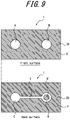
- FIG. 9 is a schematic plan view of the front surface and the back surface of the test chip 1 according to one embodiment.
- the test chip 1 illustrated in FIG. 9 is essentially same as that of FIG. 2 , except the features that the liquid flow section D provided in the second layer 20 on the back surface side has an annular structure, and formed therein with a liquid non-flow section D'.
- the test chip 1 due to the presence of the liquid non-flow section D', when the test liquid advances from the liquid flow section D toward the detection confirmation section B, there can be induced a liquid flow from the outside to the center in the detection confirmation section B. Therefore, the color development can be further effectively maintained near the center of the detection confirmation section B, so that unevenness of the color development can be suppressed even more significantly.
- the liquid flow section D having an annular structure may have any contour shape such as circle, ellipse, or rectangle, though it is preferred that the contour shape substantially matches the detection confirmation portion B in the plan view of the test chip. Further, it is preferred that the liquid non-flow section D' in the plan view of the test chip has a shape obtained by scale-reduction of the contour shape of the liquid flow section D. Further, it is preferred that the liquid non-flow section D' is colored in white, transparent, or uncolored so as not to disturb confirmation of the color development in the detection confirmation section B.
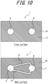
- FIG. 10 is a schematic plan view of the front surface and the back surface of the test chip 1 of another embodiment.
- the test chip 1 illustrated in FIG. 10 is generally the same as that of FIG. 2 , except that the second layer 20 arranged on the back surface side has a plurality of liquid passages E (two in FIG. 10 , i.e., E1 and E2).
- E1 and E2 a plurality of liquid passages E
- the momentum of the liquid flow from each liquid passage E is cancelled so as to promote the liquid flow in the thickness direction of the test chip 1. Therefore, the color development site can be further effectively maintained near the center of the detection confirmation section B, so as to even more significantly suppress the unevenness of the color development.
- a plurality of liquid passages F may be provided as many as the number of liquid passages E, and the plurality of liquid passages F of the first layer 10 and the plurality of liquid passages E of the second layer 20 may be connected to each other, respectively.
- FIG. 11 is a schematic plan view of the front surface and the back surface of the test chip 1 of another embodiment.
- the test chip 1 illustrated in FIG. 11 is a combination of the features illustrated in FIG. 9 and the features illustrated in FIG. 10 . With such a test chip 1 also, uneven color development can be suppressed even more significantly.
- FIG. 12 is a schematic plan view of the front surface and the back surface of the test chip 1 of another embodiment.
- the test chip 1 illustrated in FIG. 12 is generally the same as that of FIG. 11 , except that the second layer 20 arranged on the back surface side has three liquid passages E (E3 in addition to E1 and E2).
- the three liquid passages E are connected to the liquid flow section D so as to face each other. With such a test chip 1 also, uneven color development can be suppressed even more significantly.
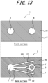
- FIG. 13 is a schematic plan view of the front surface and the back surface of the test chip 1 of another embodiment.
- the test chip 1 illustrated in FIG. 13 is substantially the same as FIG. 12 except that the liquid passage E3 is branched into two (E31 and E32) and is connected to the liquid flow section D. With such a test chip 1 also, uneven color development can be suppressed even more significantly.
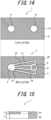
- FIG. 14 is a schematic plan view of the front surface and the back surface of the test chip 1 of another embodiment.
- the test chip 1 illustrated in FIG. 14 is substantially the same as FIG. 11 except that it has two liquid passages E (E3 and E4) in addition to the liquid passages E1 and the liquid passage E2.
- the four liquid passages E are connected to the liquid flow section D so as to face each other. With such a test chip 1 also, uneven color development can be suppressed even more significantly.
- the number of the liquid passages E (and the liquid passages F in the case of the second aspect) is preferably four or less, more preferably three or less, and further preferably two or less. Further, the number of connection(s) of the liquid passages E to the liquid flow section D is preferably four or less, more preferably three or less, and further preferably two or less.
- the test chip 1 as illustrated in FIGS. 10 to 14 , it is preferred that at least two of the plurality of liquid passages E are connected to the liquid flow section D so as to face each other.
- the test liquid advances from the liquid flow section D toward the detection confirmation section B, it is possible to concentrate the liquid flow from each liquid passage E near the center of the liquid flow section D, and to promote the flow of liquid in the thickness direction of the test chip 1. Therefore, the color development site can be further effectively maintained near the center of the detection confirmation section B to even more significantly suppress unevenness of the color development.
- the test chip 1 as described above as illustrated in FIGS. 10 to 14 , it is preferred that at least two of the plurality of liquid passages E have substantially the same shape. In this case, since the liquid flowing through the liquid passage E can reach the liquid flow section D and the detection confirmation section B almost simultaneously, it is possible to avoid the drift and further significantly suppress the unevenness of the color development.
- the material M the material that permits flow of the test liquid by capillary action
- the material M' the material in which the material M is impregnated with the hydrophobic material to prohibit flow of the test liquid
- the impregnation rate of the hydrophobic material into the material M is preferably in the range of 14% or more and 32% or less.
- test chip so that the impregnation rate is 32% or less, it is possible to sufficiently avoid the problem such as blockage when impregnating the material M with the hydrophobic material are sufficiently avoided, and more reliably obtain a test chip with a desired passage structure.
- the above-mentioned impregnation rate refers to the impregnation rate of the material M' in the region of the test chip 1 that is made of that material M' over the entire thickness direction.
- the impregnation rate may be regarded as 100% for the material M' which is obtained by immersing the material M in a hydrophobic material that is heated (e.g., heated to 120°C) to have a sufficiently low viscosity, and maintaining this temperature for a sufficient time (e.g., for 3 minutes). More specifically, the impregnation rate may be determined by the method described hereinafter with reference to the examples.
- the impregnation rate may be adjusted, for example, by regulating the amount of the hydrophobic material to be impregnated (the thickness of the hydrophobic film, etc.).
- the ratio of the thickness (t2) of the second layer 20 to the thickness (t1) of the first layer 10 i.e., the ratio t2/t1 is 0.56 or more and 2.2 or less.
- the ratio t2/t1 is preferably more than 1.0, i.e., the thickness t2 of the second layer 20 is larger than the thickness t1 of the first layer 10 as illustrated in FIG. 15 , more preferably 1.3 or more, and further preferably 1.8 or more. It is noted that the ratio t2/t1 is not particularly limited, and may be 3.0 or less.
- the above-mentioned test chip 1 may be manufactured, for example, by providing a predetermined portion (detection confirmation section B, etc.) on a sheet-shaped material to form the first layer 10, and a predetermined portion (liquid flow section D, etc.) on another sheet-shaped material to form the second layer 20, and then laminating these two sheet-like materials.
- the above-mentioned test chip 1 may also be manufactured by providing a predetermined portion on a part of a single sheet-like material to form the first layer 10, and a predetermined portion on another part of the single sheet-like material to form the second layer 20, and folding the single sheet-like material which positioning the first layer and the second layer.
- the test chip 1 according to of the present embodiment is manufactured by forming a first layer on one surface side of a single sheet-like material and forming a second layer on the other surface side.
- the test chip of the present embodiment in which the first layer and the second layer are formed on both sides of one sheet-like material, provides various advantages, such as (1) the labor and cost of lamination process (or folding process) can be saved; (2) the flow of the test liquid due to the capillary action between the first layer and the second layer is ensured; and (3) no jigs or the like for holding the laminated body (or the folded body) of the sheet-like material are required so that the disposal becomes easy.
- test chip 1 in which the first layer and the second layer are formed on both sides of a single sheet-like material may be manufactured, for example, by the method for manufacturing a test chip described below.
- a method for manufacturing a test chip as described above which is characterized in that the method comprises:
- a hydrophobic material is used to form a first hydrophobic film on a first substrate and a second hydrophobic film on a second substrate.
- a colorant may be added to the hydrophobic material.
- the hydrophobic material may be appropriately blended with a viscosity adjusting component (e.g., resin or the like), a dispersion aid, a filler, etc.
- a viscosity adjusting component e.g., resin or the like
- a dispersion aid e.g., a filler, etc.
- the hydrophobic material and the colorant are as described above with reference to the test chip.
- the above-mentioned hydrophobic material is preferably heated and melted in forming the films.
- the heating temperature may be appropriately set in consideration of the melting point of the hydrophobic material and the viscosity adjusting component.
- the viscosity of the hydrophobic material at the time of melting may be appropriately selected so that the sheet-like material can be impregnated as desired, in consideration of the thickness and basis weight (density) of the sheet-like material to be used later.
- the viscosity of the hydrophobic material is not particularly limited; however, from the viewpoint of sufficiently avoiding problems such as blockage during impregnation, the viscosity at 140°C and a shear rate of 3000 s-1 is preferably 100 mPa ⁇ s or less. , 50 mPa ⁇ s or less, more preferably 30 mPa ⁇ s or less.
- the first substrate and the second substrate are not the constituent members of the finally obtained test chip, but one of the members used for manufacturing the test chip.
- the first substrate and the second substrate for example, there may be used a film made of polyesters, such as polyethylene terephthalate (PET) and polyethylene naphthalate (PEN), as well as polyphenylene sulfide (PPS), cellophane or the like.
- PET polyethylene terephthalate
- PEN polyethylene naphthalate
- PPS polyphenylene sulfide
- the first substrate and the second substrate may have any shape such as a ribbon shape and a film shape. Further, the same substrate may be used as the first substrate and the second substrate.
- the hydrophobic film may be formed on the first substrate and the second substrate by applying the above-mentioned hydrophobic material. At the time of coating, it is preferred to heat and hold the first substrate and the second substrate in advance.
- the thickness of the first hydrophobic film and the second hydrophobic film to be formed may be appropriately selected, in consideration of the thickness of the sheet-like material to be used later.
- the ratio of the thickness of the second hydrophobic membrane (t2') to the thickness of the first hydrophobic membrane (t1') is preferably 0.56 or more and 2.2 or less.
- the t2'/t1' is more preferably more than 1.0, further preferably 1.3 or more, and even more preferably 1.8 or more.
- the ratio t2'/t1' is not particularly limited and may be 3.0 or less.
- the first hydrophobic film formed on the first substrate is used for carrying out printing on a first sacrificial substrate.
- the second hydrophobic film on the second substrate is used for carrying out printing on a second sacrificial substrate.
- the first sacrificial substrate and the second sacrificial substrate are not the constituent members of the finally obtained test chip, but one of the members used for manufacturing the test chip.
- the first sacrificial substrate and the second sacrificial substrate are preferably for general-purposes, with which printing may be carried out with high accuracy, and may be high-quality paper, coated paper, synthetic paper, etc.
- the first sacrificial substrate and the second sacrificial substrate may be comprised of the same base material.
- the printing on the first sacrificial substrate and the printing on the second sacrificial substrate are not particularly limited; for example, there may be preferably used a label writer widely used as office supplies.
- the first hydrophobic film on the first substrate is used to vary out printing on the first sacrificial substrate so as to have an inverted pattern of the first layer of the test chip.
- the second hydrophobic film on the second substrate is used to carry out printing on the second sacrificial substrate so as to have an inverted pattern of the second layer of the test chip.
- the pattern printed on the first sacrificial substrate is a pattern having a printed film corresponding to the liquid receiving section A and the detection confirmation section B.
- the pattern printed on the second sacrificial substrate is a pattern having a printed film corresponding to the liquid flow section C, the liquid flow section D, and the liquid passage E.
- the pattern to be printed may be generated in advance by, for example, a personal computer or the like, and the data may be imported to the printing device. Further, the first printing step and the second printing step may be carried out simultaneously.
- the first hydrophobic film after the first printing step is transferred to one surface of a single sheet-like material, and impregnated into the sheet-like material.
- the second hydrophobic film after the second printing step is transferred to the other surface of the single sheet-like material, and impregnated into the sheet-like material.
- a transfer device such as laminator, may be used for the transfer of the hydrophobic films. Further, in the transfer of the first hydrophobic film on the first substrate and the transfer of the second hydrophobic film on the second substrate, it is preferred that the respective transfer positions are appropriately adjusted according to the pattern of the desired test chip.
- the sheet-like material is as described above with respect to the material M.
- the impregnation of the hydrophobic membrane into the sheet-like material may be achieved, for example, by heating.
- a transfer device such as a heatable laminator
- the first transfer step and the second transfer step at least a part of the first hydrophobic film transferred from the first substrate and the second hydrophobic film transferred from the second substrate by means of the above-mentioned impregnation is made to contact in the material M.
- the hydrophobic films are impregnated over the entire thickness direction.
- the other surface is not impregnated.
- Such adjustment may be carried out, for example, by appropriately adjusting the viscosity of the above-mentioned hydrophobic material, the thickness of the sheet-like material, the thickness of the hydrophobic membrane, etc.
- the entirety of the transferred hydrophobic films may be impregnated in the sheet-like material.
- the thickness of the sheet-like material does not significantly change before and after the first transfer step and the second transfer step (there is however a possibility that the thickness may decrease due to the influence of compression by the laminator, or the like).
- the first transfer step may be carried out before the second transfer step or after the second transfer step.
- the first transfer step and the second transfer step may be carried out collectively and simultaneously.
- the sheet-like material may be sandwiched between the first substrate and the second substrate so that the hydrophobic films are brought into contact with the sheet-like material.
- the thicknesses ratio (t2/t1) of the first layer and the second layer formed after impregnation is maintained at the thickness ratio of each hydrophobic film before impregnation.
- the first substrate and the second substrate may be peeled off, as appropriate. In this way, it is possible to finally obtain the test chip of the present embodiment.
- test chips by carrying out the predetermined printing step and transfer step described above, even if a sheet-like material with a relatively rough surface such as a commercially available filter paper is used, transfer defects and voids are less likely to occur, and test chips can be manufactured with higher accuracy.
- the method for manufacturing a test chip according to the present embodiment since the first layer and the second layer having a desired pattern can be formed without using a mold or the like, on-demand manufacturing is made possible.
- test chip manufacturing method since the test chip are manufactured by forming the first layer and the second layer on both sides of one sheet-shaped material, various advantages can be achieved as compared, for example, to the case where the test chip is manufactured by using two sheet-shaped materials (or where a single sheet-shaped material is folded), such as (1) the labor and cost of lamination process (or folding process) can be saved; (2) the flow of the test liquid due to the capillary action between the first layer and the second layer of the obtained test chip is ensured; and (3) no jigs or the like for holding the laminated body (or the folded body) of the sheet-like material are required so that the disposal becomes easy.
- the inventors examined the effects of the pattern (passage structure) of the first layer and the second layer of the test chip on the color unevenness.
- Paraffin wax as a hydrophobic material (“Paraffin Wax - 155" manufactured by Nippon Seiki Co., Ltd.) 48 parts by mass, synthetic wax as a hydrophobic material (“Diacama ® 80" manufactured by Mitsubishi Chemical Corp.) 48 parts by mass, ethylenevinyl acetate copolymer resin ("Ultrasen ® 681” manufactured by Toso Corp.) 2 parts by mass, and carbon black as a coloring agent ("MA-100" manufactured by Mitsubishi Chemical Corp.) 2 parts by mass were blended and melt-mixed at 100°C. At that time, each component was dispersed using a sand mill. In this way, the hydrophobic material was been prepared.
- hydrophobic material and a substrate polyester film "Lumirror ® #5A-F531" manufactured by Toray Ind. Inc., with one side subjected to heat-resistant treatment
- a hot plate maintained at 120°C, with the non-heat-resistant side upside.
- the above-mentioned hydrophobic material was maintained in a molten state at 120°C and then applied onto the substrate with a Mayer bar to have a thickness of about 6 to 12 ⁇ m, so as to form ribbon-shaped hydrophobic films (the first hydrophobic film and the second hydrophobic film).
- the above-mentioned hydrophobic film was printed on a high-quality paper as the first sacrificial substrate so as to have a desired pattern prepared in advance on a personal computer.
- the above-mentioned hydrophobic film was printed on the high-quality paper as the second sacrificial substrate so as to have a desired pattern prepared in advance on a personal computer.
- the above two patterns printed on wood-free paper correspond to the inverted patterns of the front surface (first layer) and the back surface (second layer) of the finally obtained test chip, respectively.
- the high-quality paper after the printing is not for use in a subsequent process.
- the patterns on the front surface (the first layer) and the pattern on the back surface (the second layer) are as illustrated in FIG. 16 . That is, in Comparative Example 1, the liquid receiving section A and the detection confirmation section B are connected by a liquid passage on the front surface, and the patterns of the front surface and the back surface are substantially the same. Further, in Examples 1-1 to 1-7, the pattern of the front surface (first layer) and the pattern of the back surface (second layer) are as illustrated in FIGS. 2 , 9 , 10 , 11 , 12 , 13 and 14 , respectively.
- a filter paper (Whatman grade 41) as the sheet-shaped material M was sandwiched while carrying out appropriate positioning, and bringing the hydrophobic films into contact with the filter paper. Then, by using the laminator maintained at 90°C, the hydrophobic films were collectively transferred onto both sides of the filter paper. Each hydrophobic film was substantially completely impregnated into the filter paper from both sides, to make the portion of the filter paper directly underneath hydrophobic.
- the first layer having a predetermined pattern was formed on the front surface side of the filter paper, and the second layer having the predetermined pattern was formed on the back surface side of the filter paper.
- the hydrophobic films were impregnated over the entire thickness direction. Further, in the region where the hydrophobic film was transferred onto only one surface in the thickness direction, the impregnation did not reach the other surface. Then, the substrates on both sides were peeled off, to finally obtain a test chip. Since the first layer and the second layer in each example are derived from the same hydrophobic film, they had the same thickness.
- the front surface (the first layer) was placed on the upper side, and the center of the detection confirmation section B was marked with a water-based red highlight pen. Then, three drops of distilled water were dropped into the liquid receiving portion A with a dropper, and the change of the red mark due to the flow of water was observed.
- Comparative Example 1 As a result, in Comparative Example 1 ( FIG. 16 ), the red mark in the center of the detection confirmation section B moved toward the outer periphery of the detection confirmation section B (particularly, the side farther from the liquid receiving section A), and it was difficult to confirm the red color by visual observation. Thus, the test chip of Comparative Example 1 was recognized to have uneven color development, and is therefore unsuitable for quantitative analysis.
- Examples 1-1 to 1-7 ( FIGS. 2 , 9 to 14 ) the highlight mark in the center of the detection confirmation section B remained inside the outer periphery of the detection confirmation section B.
- Examples 1-2 to 1-7 ( FIGS. 9 to 14 ) the highlighter mark in the center of the detection confirmation section B stayed closer to the center of the detection confirmation section B. It is considered that this is because the liquid passage is optimized so that water can flow three-dimensionally in the filter paper, as compared with Comparative Example 1.
- the test chips of Examples 1-1 to 1-7 were recognized to significantly suppress the color unevenness and, therefore, quantitative analysis can be expected.
- the inventors examined the relationship between the thicknesses of the first layer and the second layer, which can ensure good liquid flowability.
- Hydrophobic materials were prepared according to the formulation as listed in Table 1.
- Table 1 Ink 1 Ink 2 Paraffin wax ⁇ 1 Parts by mass 72.0 72.0 Synthetic wax ⁇ 2 18.0 18.0 Carbon black ⁇ 3 1.8 1.8 Resin ⁇ 4 11.25 9.0 Viscosity (140°C,3000/s) mPa ⁇ s 23 17 Density g/cm 3 0.85 0.85 * 1 "Paraffin Wax -135" by Nippon Seiro Co., Ltd., * 2 Synthetic wax "Diacarna ® 30", by Mitsubishi Chemical Corp. * 3 Carbon black “MA-100” by Mitsubishi Chemical Corp. * 4 Resin " Ultrasen ® 722 " by Tosoh Corp.
- Test chips were obtained in essentially the same way as above, except that ink 1 or ink 2 was used as the hydrophobic material, Watman grade 41 (filter paper # 41) or Whatman grade 40 (filter paper # 40) was used as the filter paper (material M), and the temperature of the laminator was appropriately adjusted. At that time, the patterns of the first layer and the second layer were as illustrated in FIG. 11 . At that time, the thickness of the first hydrophobic film for forming the first layer and the thickness of the second hydrophobic film for forming the second layer (corresponding to the thickness ratio of the first layer and the second layer) were changed as appropriate.
- Each of the obtained test chips was placed, with the front surface (first layer) on the upper side.
- about 0.3 mL of a liquid obtained by dissolving aqueous fluorescent ink in distilled water was dropped into the liquid receiving section A with a dropper, to measure the time (flow time) from the start of the dropping until the liquid reaches the detection confirmation section B.
- the same measurement was carried out eight times, for calculating the average value and the standard deviation.
- Tables 2 to 5 for each combination of the hydrophobic material and the filter paper.
- Example 2 (By using ink 1 and filter paper #41) Example 2-1 Example 2-2 Example 2-3 Example 2-4 Example 2-5 Example 2-6 Example 2-7 Example 2-8 Example 2-9 Thickness of first hydrophobic film [ ⁇ m] 6 6 6 6 10.1 10.1 108 108 Thickness of second hydrophobic film [ ⁇ m] 6 10.1 10.8 11.8 12.6 6 10.1 6 108 Total thickness of hydrophobic films [ ⁇ m] 12 (min) 16.1 16.8 17.8 18.6 16.1 20.2 16.8 21.6 (max) Thickness of second hydrophobic film/ thickness of first hydrophobic film - 1.0 1.7 1.8 2.0 2.1 0.59 1.0 0.56 1.0 Average flow time [sec] 56.35 55.72 49.13 46.56 52.23 66.78 41.12 53.69 50.17 Standard deviation of flow time - 11.89 8.46 6.10 4.94 3.58 13.77 3.63 13.04 4.78 Table 3 (By using ink 2 and filter paper #41) Example 3-1 Example 3-2 Example 3-3 Example 3-4 Example 3-5 Example 3-6
- the inventors examined the impregnation rate of the hydrophobic material that can ensure good liquid flowability.
- the same filter paper (the filter paper # 41 or the filter paper # 40) as used in Experiment 2 was cut into a size of 5 cm ⁇ 2 cm, and dried at 120°C for 3 minutes, to measure the dry mass M0 (g). Then, the filter paper was immersed in the same hydrophobic material (ink 1 or ink 2) as that used in Experiment 2, and left at 120°C for 3 minutes. The filter paper after immersion was sandwiched between the same type of filter paper and slide glass, and left at 120 °C. for 1 minute under a load of 100 gf to remove excess hydrophobic material. The mass M1 (g) of the filter paper was then measured. The maximum impregnation amount Pmax (g/m 2 ) per unit section area was then calculated from (M1-M0) ⁇ 1000.
- the present disclosure provides a test chip wherein the target substance contained in the test liquid is reacted with the pre-charged labeling medium for confirming the presence of the target substance by the reaction between, and wherein uneven color development is significantly suppressed. Further, the present disclosure also provides a method for manufacturing a test chip, with which the above-mentioned test chip can be easily manufactured with high accuracy and at low cost.
Landscapes
- Health & Medical Sciences (AREA)
- Chemical & Material Sciences (AREA)
- Life Sciences & Earth Sciences (AREA)
- Immunology (AREA)
- Physics & Mathematics (AREA)
- Analytical Chemistry (AREA)
- General Health & Medical Sciences (AREA)
- General Physics & Mathematics (AREA)
- Biochemistry (AREA)
- Pathology (AREA)
- Engineering & Computer Science (AREA)
- Chemical Kinetics & Catalysis (AREA)
- Hematology (AREA)
- Molecular Biology (AREA)
- Biomedical Technology (AREA)
- Plasma & Fusion (AREA)
- Urology & Nephrology (AREA)
- Clinical Laboratory Science (AREA)
- Biotechnology (AREA)
- Microbiology (AREA)
- Food Science & Technology (AREA)
- Medicinal Chemistry (AREA)
- Cell Biology (AREA)
- Investigating Or Analysing Biological Materials (AREA)
- Investigating Or Analyzing Non-Biological Materials By The Use Of Chemical Means (AREA)
- Automatic Analysis And Handling Materials Therefor (AREA)
- Surface Acoustic Wave Elements And Circuit Networks Thereof (AREA)
- Ceramic Capacitors (AREA)
- Fixed Capacitors And Capacitor Manufacturing Machines (AREA)
Abstract
Description
- This disclosure relates to a test chip and a method for manufacturing the same.
- There is an idea that diagnosis carried out in the immediate vicinity of patients or the like (on-the-spot diagnosis) is highly important, and such an idea is being generally accepted in clinical practice. Based on such idea, test chips have been developed that enable practical analysis by providing a sheet-shaped substrate with micro-sized passages and reaction spots.
- One example of such test chip includes a mechanism wherein, when a test liquid containing a target substance such as antigen is introduced, the test liquid flows through a passage and reacts with a labeling medium, such as antibody that has been charged in advance, thereby allowing the presence of the target substance to be confirmed by means of color development (revelation). A typical example is pregnancy test drug.
- As the test chip described above, there has been reported a microfluidic device in which a paper is used as a base material and a passage or a reaction spot is formed on the paper using a wax printer or an inkjet printer (Whiteside et al., Analytical Chemistry, Vol. 82, No. 1, January 1, 2010 (NPL 1)). Such devices are also referred to as "µ-PADs (microfluidic paper-based analytical devices)" and have many advantages, such as (1) low cost, (2) pumpless, (3) no requirement for large-scale equipment, and (4) easy disposal. Research for improvement in such µ-PADs is being promoted globally.
- For example,
WO 2012/160857 A (PTL 1) discloses that the test tip can be manufactured easily and at low cost, by printing the outer edge of the passage or reaction spot as described above on a paper with ultraviolet curable ink, and curing the ink by irradiating with ultraviolet rays. - PTL 1:
WO 2012/160857 A - NPL 1: Whiteside et al., Analytical Chemistry, Vol. 82, No. 1, January 1, 2010
- However, in the conventional test chip including the technology disclosed in
PTL 1 described above, unevenness in color development (color development) tends to occur and cause fluctuation in the inspection results (insufficient reproducibility). For example, as the color development occurs near the end of the detection area, there is a problem that visual observation is difficult. Such a problem may adversely affect the diagnosis of important diseases, etc. Thus, the conventional test chip has a room for improvement in terms of suppressing uneven color development. - Further, for the above-mentioned test chips such as µ-PADs, in addition to confirmation of the presence or absence of the substance to be detected, it is desirable to realize the quantification thereof. In this regard, if it is unevenness of color development (color development) as described above can be suppressed, then it is possible to realize quantification by specifying the area of the color-developed part in the test chip and applying the pixel analysis technology. From this viewpoint also, it is desired to suppress uneven color development.
- The task underlying the present disclosure is to solve the above-mentioned problems in the conventional device and to achieve the objects as follows. That is, it is an object of the present disclosure to provide a test chip wherein the target substance contained in the test liquid is reacted with the pre-charged labeling medium for confirming the presence of the target substance by the reaction between, and wherein uneven color development is significantly suppressed. It is another object of the present disclosure to provide a method for manufacturing the above-mentioned test chip, with which the test tip can be manufactured easily, high accurately and at low cost.
- In the course of solving the above problem, the inventors found for the first time that the problem in the conventional test chip of the occurrence of color development near the end of the detection area is caused by the momentum of the liquid flow reaching the detection area.
- Further, the inventors conducted extensive studies and found that color development could be induced near the center of the detection area if the liquid passage is optimized so that the liquid can reach the detection area from the thickness direction of the sheet, which led to the completion of the present disclosure.
- The means for achieving the above object is summarized in the following clauses.
- <1> A sheet-shaped test chip comprising:
- a first layer on a front surface side and a second layer on a back surface side;
- wherein the first layer and the second layer are adjacent to each other;
- wherein one of the first layer and the second layer has a liquid receiving section A;
- wherein the first layer has at least a detection confirmation section B;
- wherein the second layer has at least a liquid flow section D adjacent to the detection confirmation section B, and a liquid passage E connected to the liquid flow section D;
- wherein, in case where the liquid receiving section A is provided in the first layer, the liquid receiving section A is spaced from the detection confirmation section B;
- wherein, when a sample test liquid is dropped into the liquid receiving section A, the test liquid passes through the liquid receiving section A, the liquid passage E, and the liquid flow section D in the stated order, by means of capillary action, and flows to the detection confirmation section B; and
- wherein the first layer is formed on one surface of a single sheet-like material, and the second layer is formed on the other surface of the sheet-like material.
- <2> A sheet-shaped test chip comprising:
- a first layer on a front surface side and a second layer on a back surface side;
- wherein the first layer and the second layer are adjacent to each other;
- wherein one of the first layer and the second layer has a liquid receiving section A;
- wherein the first layer has at least a detection confirmation section B;
- wherein the second layer has at least a liquid flow section D adjacent to the detection confirmation section B, and a liquid passage E connected to the liquid flow section D;
- wherein, in case where the liquid receiving section A is provided in the first layer, the liquid receiving section A is spaced from the detection confirmation section B;
- wherein, when a sample test liquid is dropped into the liquid receiving section A, the test liquid passes through the liquid receiving section A, the liquid passage E, and the liquid flow section D in the stated order, by means of capillary action, and flows to the detection confirmation section B; and
- wherein the liquid flow section D has an annular structure formed with a liquid non-flow section D' therein.
- <3> A sheet-shaped test chip comprising:
- a first layer on a front surface side and a second layer on a back surface side;
- wherein the first layer and the second layer are adjacent to each other;
- wherein one of the first layer and the second layer has a liquid receiving section A;
- wherein the first layer has at least a detection confirmation section B;
- wherein the second layer has at least a liquid flow section D adjacent to the detection confirmation section B, and a liquid passage E connected to the liquid flow section D;
- wherein, in case where the liquid receiving section A is provided in the first layer, the liquid receiving section A is spaced from the detection confirmation section B;
- wherein, when a sample test liquid is dropped into the liquid receiving section A, the test liquid passes through the liquid receiving section A, the liquid passage E, and the liquid flow section D in the stated order, by means of capillary action, and flows to the detection confirmation section B; and
- wherein the second layer is provided with a plurality of the liquid flow sections E.
- <4> The test chip according to <3>, wherein at least two of the liquid passages E are connected to the liquid flow section D so as to face each other.
- <5> The test chip according to <3> or <4>, wherein at least two of the liquid passages E have substantially the same shape.
- <6> The test chip according to any one of <1> to <5>, wherein:
- the first layer comprises the liquid receiving section A that is spaced from the detection confirmation section B, the second layer comprises the liquid flow section C adjacent to the liquid receiving section A; and
- the test tip is configured such that, when the sample test liquid is dropped into the liquid receiving section A, the test liquid passes through the liquid receiving section A, the liquid flow section C, the liquid passage E, and the liquid flow section D in this order, due to a capillary action and flows to the detection confirmation section B.
- <7> The test chip according to any one of <1> to <5>, wherein:
- the first layer comprises the liquid receiving section A that is spaced from the detection confirmation section B, and the liquid passage F that is connected to the liquid receiving section A; and
- the test tip is configured so that, when the test liquid is dropped into the liquid receiving section A, the test liquid passes through the liquid receiving portion A, the liquid passage F, the liquid passage E, and the liquid flow section D in this order, due to the capillary action.
- <8> The test chip according to any one of <1> to <5>, wherein the second layer comprises the liquid receiving portion A.
- <9> The test chip according to any one of <1> to <8>, wherein:
- the liquid receiving section A, any liquid flow section C, any liquid passage F, the liquid passage E, the liquid flow section D, and the detection confirmation section B, are made of a material M that permits flow of the test liquid by means of capillary action; and
- the part other than the material M is made of a material M' in which the material M is impregnated with the hydrophobic material that prohibits flow of the test liquid.
- <10> The test chip according to <9>, wherein the material M is a filter paper.
- <11> The test chip according to <9> or <10> wherein, in the material M', an impregnation rate of the hydrophobic material into the material M is 14% or more and 32% or less.
- <12> The test chip according to any one of <1> to <11>, wherein a ratio of the thickness of the second layer to the thickness of the first layer (thickness of the second layer / thickness of the first layer) is 0.56 or more and 2.2 or less.
- <13> The test chip according to any one of <1> to <12>, wherein a color development reaction due to a substance to be detected takes place in the detection confirmation section B.
- <14> A method for manufacturing a test chip of any one of <1> to <13>, comprising:
- a film formation step wherein a hydrophobic material is used for forming a first hydrophobic film on a first substrate, and a second hydrophobic film on a second substrate;
- a first printing step wherein the first hydrophobic film on the first substrate is used for carrying out printing on a first sacrificial substrate, so as to be of an inverted pattern of a first layer of the test chip;
- a second printing process wherein the second hydrophobic film on the second substrate is used for carrying out printing on a second sacrificial substrate, so as to be of an inverted pattern of the second layer of the test chip;
- a first transfer step wherein the first hydrophobic film after the first printing step is transferred onto one surface of a single sheet-like material and impregnated into the sheet-like material; and
- a second transfer step wherein the second hydrophobic film after the second printing step is transferred onto the other surface of the single sheet-like material and impregnated into the sheet-like material.
- <15> The method for manufacturing a test chip according to <14>, wherein a ratio of the thickness of the second hydrophobic membrane to the thickness of the first hydrophobic membrane (thickness of the second hydrophobic membrane / thickness of the first hydrophobic membrane) is 0.56 or more and 2.2 or less.
- According to the present disclosure, it is possible to provide a test chip wherein the target substance contained in the test liquid is reacted with the pre-charged labeling medium for confirming the presence of the target substance by the reaction between, and wherein uneven color development is significantly suppressed. Furthermore, according to the present disclosure, it is also possible to provide a method for manufacturing the above-mentioned test chip, with which the test tip can be manufactured easily, high accurately and at low cost.
-
-
FIG. 1A is a schematic perspective view of the test chip according to one embodiment of the present disclosure. -
FIG, 1B is a schematic perspective view of the test chip ofFIG. 1A . -
FIG. 2 is a schematic plan view of the front surface and the back surface of the test chip ofFIG. 1A . -
FIG. 3 is a schematic cross-sectional view of the test chip ofFIG. 1A . -
FIG. 4 is the schematic exploded view of the test chip according to one embodiment of the present disclosure. - I
FIG. 5 is a schematic plan view of the front surface and the back surface of the test chip according to one embodiment of the present disclosure. -
FIG. 6 is a schematic cross-sectional view of the test chip ofFIG. 5 . -
FIG. 7 is a schematic plan view of the front surface and the back surface of the test chip according to one embodiment of the present disclosure. -
FIG. 8 is a schematic cross-sectional view of the test chip ofFIG. 7 . -
FIG. 9 is a schematic plan view of the front surface and the back surface of the test chip according to one embodiment of the present disclosure. -
FIG. 10 is a schematic plan view of the front surface and the back surface of the test chip according to one embodiment of the present disclosure. -
FIG. 11 is a schematic plan view of the front surface and the back surface of the test chip according to one embodiment of the present disclosure. -
FIG. 12 is a schematic plan view of the front surface and the back surface of the test chip according to one embodiment of the present disclosure. -
FIG. 13 is a schematic plan view of the front surface and the back surface of the test chip according to one embodiment of the present disclosure. -
FIG. 14 is a schematic plan view of the front surface and the back surface of the test chip according to one embodiment of the present disclosure. -
FIG. 15 is a schematic cross-sectional view of the test chip according to one embodiment of the present disclosure. -
FIG. 16 is a schematic plan view of the front surface and the back surface of the test chip according to one embodiment of the present disclosure. - Hereinafter, the present disclosure will be described in detail based on the embodiments.
- According to the present disclosure, there is provided a sheet-shaped test chip, which is basically characterized in that it includes
- a first layer on a front surface side and a second layer on a back surface side;
- wherein the first layer and the second layer are adjacent to each other;
- wherein one of the first layer and the second layer has a liquid receiving section A;
- wherein the first layer has at least a detection confirmation section B;
- wherein the second layer has at least a liquid flow section D adjacent to the detection confirmation section B, and a liquid passage E connected to the liquid flow section D;
- wherein, in case where the liquid receiving section A is provided in the first layer, the liquid receiving section A is spaced from the detection confirmation section B; and
- wherein, when a sample test liquid is dropped into the liquid receiving section A, the test liquid passes through the liquid receiving section A, the liquid passage E, and the liquid flow section D in the stated order, by means of capillary action, and flows to the detection confirmation section B.
- Further, the test chip according to one embodiment of the present disclosure is further characterized in that, in addition to the basic features noted above, the liquid flow section D has an annular structure formed with a liquid non-flow section D' therein. The details of this feature will be described later.
- The test chip according to another embodiment of the present disclosure is further characterized in that, in addition to the basic features noted above, the second layer is provided with a plurality of the liquid passages E. The details of this feature will be described later.
- The test chip according to still another embodiment of the present disclosure is further characterized in that, in addition to the basic features noted above, the first layer is formed on one surface of a single sheet-like material, and the second layer is formed on the other surface of the sheet-like material. The details of this feature will be described later.
- According to these test chips, it is possible to significantly suppress uneven color development.
- In the test chip of the present disclosure, the liquid receiving portion A is a portion where the test liquid is dropped. Further, in the test chip of the present disclosure, the detection confirmation section B is a portion where confirmation is made as to whether or not a target substance, such as an antigen, is present in the test liquid dropped on the liquid receiving section A, by means of the presence or absence of color development. Thus, the
test chip 1 of the present disclosure may be provided with a medium that reacts with the substance to be detected and / or a labeling medium adapted to cause a color reaction due to the substance to be detected. Furthermore, it is preferred that, in thetest chip 1 of the present disclosure, the color development reaction due to the substance to be detected takes place in the detection confirmation section B. - More specifically, the aspects of the above-mentioned basic features common to the test chips of the present disclosure may include an aspect wherein the liquid receiving section A is provided in the first layer and the second layer has the liquid flow section C (first aspect), an aspect wherein the liquid receiving section A is provided in the first layer, and the first layer is further provided with a liquid passage F connected to the liquid receiving portion A (second aspect), and an aspect wherein the liquid receiving portion A is provided in the second layer (third aspect).
-
FIGS. 1A and 1B are schematic perspective views of atest chip 1 according to the first aspect, respectively. Thetest chip 1 includes afirst layer 10 on the front surface side, that is, the surface side on which an inspector visually recognizes the inspection results during use, and asecond layer 20 on the back surface side thereof.FIG. 1A is a perspective view with the front surface of thetest chip 1 on the upper side, andFIG. 1B is a perspective view with the back surface of thetest chip 1 on the upper side. As illustrated inFIGS. 1A and 1B , thetest chip 1 is of a sheet shape. Further, thefirst layer 10 and thesecond layer 20 of thetest chip 1 do not have any intervening objects and are adjacent to each other. The shape of thetest chip 1 in a plan view is not particularly limited and may be appropriately selected depending on the intended purpose; for example, it may be rectangular as illustrated inFIGS. 1A and 1B , or may be circular, oval or the like. -
FIG. 2 is a schematic plan view of the front surface and the back surface of thetest chip 1, and the structure thereof corresponds to thetest chip 1 illustrated inFIGS. 1A and 1B . As illustrated inFIG. 2 , thetest chip 1 is provided with a liquid receiving section A and a detection confirmation section B on thefirst layer 10 that is arranged on the front surface side. The liquid receiving section A and the detection confirmation section B are spaced from each other in thefirst layer 10 of thetest chip 1. - The
first layer 10 of thetest chip 1 is provided with a liquid non-flow section X as a portion other than the liquid receiving section A and the detection confirmation section B. The liquid receiving section A and the detection confirmation section B are made, for example, of a material M that permits flow of the test liquid by capillary action. Further, the liquid non-flow section X is made, for example, of a material M' that prohibits (does not permit) flow of the test liquid. - As illustrated in
FIG. 2 , thetest chip 1 is provided with a liquid flow section C, a liquid flow section D, and a liquid passage E on thesecond layer 20 that is arranged on the back surface side. The liquid passage E is connected to the liquid flow section D and also to the liquid flow section C. Thesecond layer 20 of thetest chip 1 is provided with a liquid non-flow section Y, as a section other than the liquid flow section C, the liquid passage E, and the liquid flow section D. The liquid flow section C, the liquid passage E, and the liquid flow section D are made of a material M that permits flow of the test liquid by capillary action, as in the case of the liquid receiving section A and the detection confirmation section B described above. Further, the liquid non-flow section Y is made of a material M' that prohibits flow of the test liquid, for example, as in the case of the liquid non-flow section X described above. -
FIG. 3 is a schematic cross-sectional view, with thetest chip 1 ofFIG. 2 being cut along the line a-a. As illustrated inFIG. 3 , in thetest chip 1 according to the first aspect, the liquid receiving section A of thefirst layer 10 and the liquid flow section C of thesecond layer 20 are adjacent to each other, and the detection confirmation section B of thefirst layer 10 and the liquid flow section D of thesecond layer 20 are adjacent to each other. That is, in thetest chip 1 according to the first aspect, the liquid receiving section A, the liquid flow section C, the liquid passage E, the liquid flow section D, and the detection confirmation section B are adjacent to each other or connected to each other in this order. In other words, thetest chip 1 according to the first aspect is configured so that, the test liquid dropped into the liquid receiving section A is caused to flow eventually to the detection confirmation section B by the capillary action, via the liquid receiving section A, the liquid flow section C, the liquid passage E and the liquid flow section D in this order. - Here, in the conventional test chip, since the liquid receiving section and the detection confirmation section (detection area) are simply connected by a passage on the base material, when the test liquid is dropped into the liquid receiving section, there is a problem of unevenness of the color development such that the color development is distributed unevenly near the end of the detection area (particularly near the end that is remote from the liquid receiving section), due to the momentum of the liquid flow flowing along the surface direction of the material and reaching the detection area. On the other hand, in the
test tip 1 as described above, since thetest chip 1 has the above-mentioned configuration, the test liquid dropped into the liquid receiving section A is flows eventually in the thickness direction of the test chip 1 (the direction from the liquid flow section D to the detection confirmation section), and reaches the detection confirmation section B. Thus, in thetest chip 1 according to the first aspect, the color development site can be maintained near the center of the detection confirmation section B, thereby significantly suppressing unevenness of the color development. - As described above, the liquid receiving section A and the detection confirmation section B in the
first layer 10, and the liquid flow section C, the liquid flow section D, and the liquid passage E in thesecond layer 20 are made, for example, of the material M that permits flow of the test liquid due to the capillary action. On the other hand, the liquid non-flowing section X in thefirst layer 10 and the liquid non-flowing section Y in thesecond layer 20 are made, for example, of the material M' in which the material M is impregnated with a hydrophobic material, and flow of the test liquid is prohibited. -
FIG. 4 is a schematically exploded view of thetest chip 1 ofFIGS. 1A and 1B . As illustrated on the left side ofFIG. 4 , in a schematic sense, thetest chip 1 is comprised of the above material M, a pre-first layer 10' made of ahydrophobic material 50 having the pattern of thefirst layer 10, and a pre-second layer 20' made of ahydrophobic material 50 having a pattern of asecond layer 20. Further, as illustrated on the left side ofFIG. 4 , thetest chip 1 has a structure in which the pre-first layer 10'and the pre-second layer 20' are impregnated with the material M from both sides. Then, as illustrated on the right side ofFIG. 4 , from the viewpoint of material, thetest chip 1 is comprised, for example, of the material M and the material M' in which the material M is impregnated with thehydrophobic material 50. - The material M is not particularly limited as long as it causes a capillary action, and may include paper, such as filter paper, non-woven fabric, nitrocellulose, polypropylene, etc. Among these, from the viewpoint that a test chip can be produced more easily and at low cost, the material M is preferably a filter paper. Furthermore, the thickness and the basis weight (density) of the material M may be appropriately selected in consideration of the viscosity of the test liquid, etc.
- The hydrophobic material is not particularly limited as long as it can be impregnated into the material M and inhibits the capillary action in the material M, and examples thereof may include wax or a composition containing the same. Further, from the viewpoint of easy production, the hydrophobic material preferably has a melting point of 90°C, or lower.
- In the test chip described above, it is preferred that the material M' of the liquid non-flow section X on the front surface side is colored so that the inspector can easily observe the liquid receiving section A and the detection confirmation section B on the front surface side. On the other hand, the material M' of the liquid non-circulation portion Y on the back surface side of the test chip may be colored, white or transparent, or may not be colored.
- The coloring of the material M' may be carried out for example, by impregnating the material M with a colorant in addition to the hydrophobic material. Such a colorant is preferably hydrophobic, and examples thereof may include pigments such as carbon black (black pigment). Further, it is preferred to select a colorant that does not adversely affect the reagent used for the test chip.
- The shape of the liquid receiving portion A in a plan view is not particularly limited and may be appropriately selected depending on the intended purpose; for example, it may be circular as illustrated in
FIG. 2 , or may be elliptical, rectangular, etc. - The shape of the detection confirmation section B in a plan view is not particularly limited and may be appropriately selected depending on the intended purpose; it may be circular as illustrated in
FIG. 2 , or may be elliptical, rectangular or, etc. - The shape of the liquid flow section C in a plan view is not particularly limited and may be appropriately selected depending on the intended purpose; preferably, it is the same shape as the liquid receiving section A. Further, it is preferred that the liquid flow section C has a shape that substantially matches the liquid receiving section A in the plan view of the test chip.
- The shape of the liquid flow section D in a plan view is not particularly limited and may be appropriately selected depending on the intended purpose; preferably, it is the same shape as the detection confirmation section B. Further, it is preferred that the liquid flow section D has a shape that substantially matches the detection confirmation section B in the plan view of the test chip.
- The thickness of the test chip according to the present disclosure is not particularly limited, and may be 100 to 300 µm, for example.
- Although not illustrated, the test chip of the present disclosure may have a plurality of sets of combination of the detection confirmation section B, the liquid flow section D, and the liquid passage E. In this case, the presence or absence of a plurality of substances to be detected can be confirmed at the same time, through a single inspection.
-
FIG. 5 is a schematic plan view of the front surface and the back surface of thetest chip 1 according to the second aspect. As illustrated inFIG. 5 , thetest chip 1 is provided with a liquid receiving section A and a detection confirmation section B on thefirst layer 10 arranged on the front surface side. The liquid receiving section A and the detection confirmation section B are spaced from each other in afirst layer 10 of thetest chip 1. Further, thetest chip 1 has a liquid passage F connected to the liquid receiving portion A in thefirst layer 10 arranged on the front surface side. - Further, the
first layer 10 of thetest chip 1 is provided with a liquid non-flow section X, as a portion other than the liquid receiving section A, the detection confirmation section B, and the liquid passage F. The liquid receiving section A, the detection confirmation section B, and the liquid passage F are made, for example, of a material M that permits flow of the test liquid by the capillary action. Further, the liquid non-flow section X is made, for example, of a material M' that prohibits flow of the test liquid. - As illustrated in
FIG. 5 , thetest chip 1 is provided with a liquid flow section D and a liquid passage E in asecond layer 20 arranged on the back surface side. The liquid passage E is connected to the liquid flow section D. Further, thesecond layer 20 of thetest chip 1 is provided with a liquid non-flow section Y, as a portion other than the liquid passage E and the liquid flow section D. The liquid passage E and the liquid passage D are made, for example, of the material M that permits flow of the test liquid is expressed by the capillary action, as in the liquid receiving section A, the detection confirmation section B, and the liquid passage F described above. Further, the liquid non-flow section Y is made, for example, of a material M' that prohibits flow of the test liquid, as in the liquid non-flow section X described above. -
FIG. 6 is a schematic cross-sectional view, with thetest chip 1 ofFIG. 5 being cut along the line b-b'. As illustrated inFIG. 6 , in thetest chip 1 according to the second aspect, the detection confirmation section B of thefirst layer 10 and the liquid flow section D of thesecond layer 20 are adjacent to each other, and the liquid passage F of thefirst layer 10 and the liquid passage E of thesecond layer 20 are connected with each other. That is, in thetest chip 1 according to the second aspect, the liquid receiving section A, the liquid passage F, the liquid passage E, the liquid flow section D, and the detection confirmation section B are adjacent to each other or connected to each other in this order. In other words, thetest chip 1 according to the second aspect is configured such that, when the test liquid is dropped on the liquid receiving portion A, the test liquid passes the liquid receiving portion A, the liquid passage F, and the liquid passage E, and the liquid flow section D in this order, due to the capillary action, and eventually flows to the detection confirmation section B. Thus, in thetest chip 1 according to the second aspect, as in the first aspect, the test liquid dropped on the liquid receiving portion A is permitted to flow in the thickness direction of the test chip 1 (the direction from the liquid flow section D toward the detection confirmation section B) and to eventually reach the detection confirmation section B. Therefore, also in thetest chip 1 according to the second aspect, the color development site can be maintained near the center of the detection confirmation section B, thereby significantly suppressing unevenness of the color development. - As described above, the liquid receiving section A, the detection confirmation section B and the liquid passage F in the
first layer 10, and the liquid flow section D and the liquid passage E in thesecond layer 20 are made, for example, of a material M that permits flow of the test liquid due to the capillary action. On the other hand, the liquid non-flow section X in thefirst layer 10 and the liquid non-flow section Y in thesecond layer 20 are made, for example, of the material M' in which the material M is impregnated with a hydrophobic material, which prohibits the flow of the test liquid. - In the test chip described above, it is preferred that the material M' of the liquid non-flow section X on the front surface side is colored so that the inspector can easily observe the liquid receiving section A and the detection confirmation section B on the front surface side. On the other hand, the material M' of the liquid non-circulation portion Y on the back surface side of the test chip may be colored, white or transparent, or may not be colored.
- Other than the above, description of the features of the second aspect common to the first aspect is omitted.
-
FIG. 7 is a schematic plan view of the front surface and the back surface of thetest chip 1 according to the third aspect. As illustrated inFIG. 7 , thetest chip 1 is provided with the detection confirmation section B that is arranged in thefirst layer 10 arranged on the front surface side, but is not provided with the liquid receiving section A. - Further, the
first layer 10 of thetest chip 1 is provided with a liquid non-flow section X as a portion other than the detection confirmation section B. The detection confirmation section B is made, for example, of a material M that permits flow of the test liquid by the capillary action. Further, the liquid non-flow section X is made, for example, of a material M' that prohibits flow of the test liquid. - Further, as illustrated in
FIG. 7 , thetest chip 1 is provided with a liquid receiving section A, a liquid flow section D, and a liquid passage E on asecond layer 20 arranged on the back surface side. The liquid passage E is connected to the liquid flow section D and is also connected to the liquid receiving section A. Further, thesecond layer 20 of thetest chip 1 is provided with a liquid non-flow section Y, as a portion other than the liquid receiving section A, the liquid passage E, and the liquid flow section D. The liquid receiving section A, the liquid passage E, and the liquid flowing section D are made, for example, of a material M that permits flow of the test liquid by the capillary action, as in the detection confirmation section B described above. Further, the liquid non-flow section Y is made, for example, of a material M' that prohibits flow of the test liquid, as in the liquid non-flow section X described above. -
FIG. 8 is a schematic cross-sectional view, with thetest chip 1 ofFIG. 7 being cut along the line c-c. As illustrated inFIG. 8 , in thetest chip 1 according to the third aspect, the detection confirmation section B of thefirst layer 10 and the liquid flow section D of thesecond layer 20 are adjacent to each other. That is, in thetest chip 1 according to the third aspect, the liquid receiving section A, the liquid passage E, the liquid flow section D, and the detection confirmation section B are adjacent to each other or connected with each other in this order. In other words, thetest chip 1 according to the third aspect is configured such that the test liquid dropped into the liquid receiving portion A is caused to flow by the capillary action through the liquid receiving portion A, the liquid passage E, and the liquid flow section D in this order, and to eventually reach the detection confirmation section B. Thus, in thetest chip 1 according to the third aspect, as in the first aspect, the test liquid dropped on the liquid receiving portion A is permitted to flow in the thickness direction of the test chip 1 (the direction from the liquid flow section D toward the detection confirmation section B) and to eventually reach the detection confirmation section B. Therefore, also in thetest chip 1 according to the third aspect, the color development site can be maintained near the center of the detection confirmation section B, thereby significantly suppressing unevenness of the color development. - As described above, the detection confirmation section B and the liquid passage F in the
first layer 10, and the liquid flow section D and the liquid passage E in thesecond layer 20 are made, for example, of a material M that permits flow of the test liquid due to the capillary action. On the other hand, the liquid non-flow section X in thefirst layer 10 and the liquid non-flow section Y in thesecond layer 20 are made, for example, of a material M' in which the material M is impregnated with a hydrophobic material, which prohibits flow of the test liquid. - In the test chip described above, it is preferred that the material M' of the liquid non-flow section X on the front surface side and the liquid non-flow section Y on the back surface side is colored so that the inspector can easily observe the liquid receiving portion A and the detection confirmation portion B on the front surface side.
- The test chip according to the third aspect is particularly useful, for example, when it is desired to arrange the liquid receiving section A and the detection confirmation section B on different surfaces from the viewpoint of fail-safe.
- Other than the above, description of the features of the second aspect common to the first aspect is omitted.
- Further, the test chip according to the present disclosure may appropriately include the features described below. Hereinafter, the description will be made with reference to the features according to the first aspect as the basic feature, though any of the features may be applied to the case of the second aspect and the third aspect.
-
FIG. 9 is a schematic plan view of the front surface and the back surface of thetest chip 1 according to one embodiment. Thetest chip 1 illustrated inFIG. 9 is essentially same as that ofFIG. 2 , except the features that the liquid flow section D provided in thesecond layer 20 on the back surface side has an annular structure, and formed therein with a liquid non-flow section D'. In thetest chip 1, due to the presence of the liquid non-flow section D', when the test liquid advances from the liquid flow section D toward the detection confirmation section B, there can be induced a liquid flow from the outside to the center in the detection confirmation section B. Therefore, the color development can be further effectively maintained near the center of the detection confirmation section B, so that unevenness of the color development can be suppressed even more significantly. - In the
test chip 1 as described above, the liquid flow section D having an annular structure may have any contour shape such as circle, ellipse, or rectangle, though it is preferred that the contour shape substantially matches the detection confirmation portion B in the plan view of the test chip. Further, it is preferred that the liquid non-flow section D' in the plan view of the test chip has a shape obtained by scale-reduction of the contour shape of the liquid flow section D. Further, it is preferred that the liquid non-flow section D' is colored in white, transparent, or uncolored so as not to disturb confirmation of the color development in the detection confirmation section B. -
FIG. 10 is a schematic plan view of the front surface and the back surface of thetest chip 1 of another embodiment. Thetest chip 1 illustrated inFIG. 10 is generally the same as that ofFIG. 2 , except that thesecond layer 20 arranged on the back surface side has a plurality of liquid passages E (two inFIG. 10 , i.e., E1 and E2). In thetest chip 1, when the test liquid travels from the liquid flow section D toward the detection confirmation section B, due to the presence of a plurality of liquid passages E, the momentum of the liquid flow from each liquid passage E is cancelled so as to promote the liquid flow in the thickness direction of thetest chip 1. Therefore, the color development site can be further effectively maintained near the center of the detection confirmation section B, so as to even more significantly suppress the unevenness of the color development. - Regarding the abovementioned feature, in the case of the test chip according to the second aspect, a plurality of liquid passages F may be provided as many as the number of liquid passages E, and the plurality of liquid passages F of the
first layer 10 and the plurality of liquid passages E of thesecond layer 20 may be connected to each other, respectively. -
FIG. 11 is a schematic plan view of the front surface and the back surface of thetest chip 1 of another embodiment. Thetest chip 1 illustrated inFIG. 11 is a combination of the features illustrated inFIG. 9 and the features illustrated inFIG. 10 . With such atest chip 1 also, uneven color development can be suppressed even more significantly. -
FIG. 12 is a schematic plan view of the front surface and the back surface of thetest chip 1 of another embodiment. Thetest chip 1 illustrated inFIG. 12 is generally the same as that ofFIG. 11 , except that thesecond layer 20 arranged on the back surface side has three liquid passages E (E3 in addition to E1 and E2). In this instance, in thetest chip 1 illustrated inFIG. 12 , the three liquid passages E are connected to the liquid flow section D so as to face each other. With such atest chip 1 also, uneven color development can be suppressed even more significantly. -
FIG. 13 is a schematic plan view of the front surface and the back surface of thetest chip 1 of another embodiment. Thetest chip 1 illustrated inFIG. 13 is substantially the same asFIG. 12 except that the liquid passage E3 is branched into two (E31 and E32) and is connected to the liquid flow section D. With such atest chip 1 also, uneven color development can be suppressed even more significantly. -
FIG. 14 is a schematic plan view of the front surface and the back surface of thetest chip 1 of another embodiment. Thetest chip 1 illustrated inFIG. 14 is substantially the same asFIG. 11 except that it has two liquid passages E (E3 and E4) in addition to the liquid passages E1 and the liquid passage E2. In this instance, in thetest chip 1 illustrated inFIG. 14 , the four liquid passages E are connected to the liquid flow section D so as to face each other. With such atest chip 1 also, uneven color development can be suppressed even more significantly. - In the
test chip 1 as described above, from the viewpoint of suppressing an increase in the amount of test liquid required for inspection, the number of the liquid passages E (and the liquid passages F in the case of the second aspect) is preferably four or less, more preferably three or less, and further preferably two or less. Further, the number of connection(s) of the liquid passages E to the liquid flow section D is preferably four or less, more preferably three or less, and further preferably two or less. - Further, in the
test chip 1 as described above, as illustrated inFIGS. 10 to 14 , it is preferred that at least two of the plurality of liquid passages E are connected to the liquid flow section D so as to face each other. By this, when the test liquid advances from the liquid flow section D toward the detection confirmation section B, it is possible to concentrate the liquid flow from each liquid passage E near the center of the liquid flow section D, and to promote the flow of liquid in the thickness direction of thetest chip 1. Therefore, the color development site can be further effectively maintained near the center of the detection confirmation section B to even more significantly suppress unevenness of the color development. - Further, in the
test chip 1 as described above, as illustrated inFIGS. 10 to 14 , it is preferred that at least two of the plurality of liquid passages E have substantially the same shape. In this case, since the liquid flowing through the liquid passage E can reach the liquid flow section D and the detection confirmation section B almost simultaneously, it is possible to avoid the drift and further significantly suppress the unevenness of the color development. - When the above-mentioned
test chip 1 is comprised of the material M (the material that permits flow of the test liquid by capillary action) and the material M' (the material in which the material M is impregnated with the hydrophobic material to prohibit flow of the test liquid), it is preferred for the material M' that the impregnation rate of the hydrophobic material into the material M is preferably in the range of 14% or more and 32% or less. By manufacturing the test chip so that the impregnation rate is 14% or more, the passage wall surface (interface between the material M and the material M') of the test liquid becomes sufficiently uniform, and the flow of the test liquid from the liquid receiving section A to the detection confirmation section B can be made smoother. Further, by manufacturing the test chip so that the impregnation rate is 32% or less, it is possible to sufficiently avoid the problem such as blockage when impregnating the material M with the hydrophobic material are sufficiently avoided, and more reliably obtain a test chip with a desired passage structure. - The above-mentioned impregnation rate refers to the impregnation rate of the material M' in the region of the
test chip 1 that is made of that material M' over the entire thickness direction. - The impregnation rate may be regarded as 100% for the material M' which is obtained by immersing the material M in a hydrophobic material that is heated (e.g., heated to 120°C) to have a sufficiently low viscosity, and maintaining this temperature for a sufficient time (e.g., for 3 minutes). More specifically, the impregnation rate may be determined by the method described hereinafter with reference to the examples.
- The impregnation rate may be adjusted, for example, by regulating the amount of the hydrophobic material to be impregnated (the thickness of the hydrophobic film, etc.).
- In the
test chip 1 as described above, it is preferred that the ratio of the thickness (t2) of thesecond layer 20 to the thickness (t1) of the first layer 10 (the thickness of the second layer / the thickness of the first layer), i.e., the ratio t2/t1 is 0.56 or more and 2.2 or less. By manufacturing the test chip so that the ratio t2/t1 is 0.56 or more and 2.2 or less, a desired passage structure can be more reliably formed in the obtained test chip. In particular, when the test chip is manufactured by the test chip manufacturing method described later, if the test chip is manufactured so that the ratio t2/t1 is 0.56 or more and 2.2 or less, it is possible to sufficiently avoid problems such as blockage when impregnating the sheet-like material with the hydrophobic material, and effectively improve the speed and/or speed stability of the liquid flow from the liquid receiving section A to the detection confirmation section B. From the same viewpoint, the ratio t2/t1 is preferably more than 1.0, i.e., the thickness t2 of thesecond layer 20 is larger than the thickness t1 of thefirst layer 10 as illustrated inFIG. 15 , more preferably 1.3 or more, and further preferably 1.8 or more. It is noted that the ratio t2/t1 is not particularly limited, and may be 3.0 or less. - The above-mentioned
test chip 1 may be manufactured, for example, by providing a predetermined portion (detection confirmation section B, etc.) on a sheet-shaped material to form thefirst layer 10, and a predetermined portion (liquid flow section D, etc.) on another sheet-shaped material to form thesecond layer 20, and then laminating these two sheet-like materials. Alternatively, the above-mentionedtest chip 1 may also be manufactured by providing a predetermined portion on a part of a single sheet-like material to form thefirst layer 10, and a predetermined portion on another part of the single sheet-like material to form thesecond layer 20, and folding the single sheet-like material which positioning the first layer and the second layer. However, it is preferred that thetest chip 1 according to of the present embodiment is manufactured by forming a first layer on one surface side of a single sheet-like material and forming a second layer on the other surface side. The test chip of the present embodiment, in which the first layer and the second layer are formed on both sides of one sheet-like material, provides various advantages, such as (1) the labor and cost of lamination process (or folding process) can be saved; (2) the flow of the test liquid due to the capillary action between the first layer and the second layer is ensured; and (3) no jigs or the like for holding the laminated body (or the folded body) of the sheet-like material are required so that the disposal becomes easy. - The
test chip 1 in which the first layer and the second layer are formed on both sides of a single sheet-like material may be manufactured, for example, by the method for manufacturing a test chip described below. - According to one embodiment of the present disclosure, there is provided a method for manufacturing a test chip as described above, which is characterized in that the method comprises:
- a film formation step wherein a hydrophobic material is used for forming a first hydrophobic film on a first substrate, and a second hydrophobic film on a second substrate;
- a first printing step wherein the first hydrophobic film on the first substrate is used for carrying out printing on a first sacrificial substrate, so as to be of an inverted pattern of a first layer of the test chip;
- a second printing process wherein the second hydrophobic film on the second substrate is used for carrying out printing on a second sacrificial substrate, so as to be of an inverted pattern of the second layer of the test chip;
- a first transfer step wherein the first hydrophobic film after the first printing step is transferred onto one surface of a single sheet-like material and impregnated into the sheet-like material; and
- a second transfer step wherein the second hydrophobic film after the second printing step is transferred onto the other surface of the single sheet-like material and impregnated into the sheet-like material.
- With such manufacturing method, it is possible to manufacture the above-described test chip easily, with high accuracy and at low cost.
- In the film forming step, a hydrophobic material is used to form a first hydrophobic film on a first substrate and a second hydrophobic film on a second substrate.
- A colorant may be added to the hydrophobic material. Further, the hydrophobic material may be appropriately blended with a viscosity adjusting component (e.g., resin or the like), a dispersion aid, a filler, etc. The hydrophobic material and the colorant are as described above with reference to the test chip.
- The above-mentioned hydrophobic material is preferably heated and melted in forming the films. The heating temperature may be appropriately set in consideration of the melting point of the hydrophobic material and the viscosity adjusting component. In addition, the viscosity of the hydrophobic material at the time of melting may be appropriately selected so that the sheet-like material can be impregnated as desired, in consideration of the thickness and basis weight (density) of the sheet-like material to be used later.
- The viscosity of the hydrophobic material is not particularly limited; however, from the viewpoint of sufficiently avoiding problems such as blockage during impregnation, the viscosity at 140°C and a shear rate of 3000 s-1 is preferably 100 mPa·s or less. , 50 mPa·s or less, more preferably 30 mPa·s or less.
- The first substrate and the second substrate are not the constituent members of the finally obtained test chip, but one of the members used for manufacturing the test chip. As the first substrate and the second substrate, for example, there may be used a film made of polyesters, such as polyethylene terephthalate (PET) and polyethylene naphthalate (PEN), as well as polyphenylene sulfide (PPS), cellophane or the like. The first substrate and the second substrate may have any shape such as a ribbon shape and a film shape. Further, the same substrate may be used as the first substrate and the second substrate.
- In the film forming step, the hydrophobic film may be formed on the first substrate and the second substrate by applying the above-mentioned hydrophobic material. At the time of coating, it is preferred to heat and hold the first substrate and the second substrate in advance. The thickness of the first hydrophobic film and the second hydrophobic film to be formed may be appropriately selected, in consideration of the thickness of the sheet-like material to be used later.
- In particular, the ratio of the thickness of the second hydrophobic membrane (t2') to the thickness of the first hydrophobic membrane (t1') (thickness of the second hydrophobic film / thickness of the first hydrophobic film), that is, the ratio t2'/ t1'is preferably 0.56 or more and 2.2 or less. By setting the ratio t2'/t1' to 0.56 or more and 2.2 or less, problems such as blockage when impregnating the sheet-like material with the hydrophobic material in the subsequent process are sufficiently avoided, and the speed and/or speed stability of the liquid flow from the liquid receiving section A to the detection confirmation section B can be sufficiently increased. From the same viewpoint, the t2'/t1' is more preferably more than 1.0, further preferably 1.3 or more, and even more preferably 1.8 or more. However, the ratio t2'/t1' is not particularly limited and may be 3.0 or less.
- In the first printing step, the first hydrophobic film formed on the first substrate is used for carrying out printing on a first sacrificial substrate. Further, in the second printing step, the second hydrophobic film on the second substrate is used for carrying out printing on a second sacrificial substrate.
- The first sacrificial substrate and the second sacrificial substrate are not the constituent members of the finally obtained test chip, but one of the members used for manufacturing the test chip. The first sacrificial substrate and the second sacrificial substrate are preferably for general-purposes, with which printing may be carried out with high accuracy, and may be high-quality paper, coated paper, synthetic paper, etc. The first sacrificial substrate and the second sacrificial substrate may be comprised of the same base material.
- The printing on the first sacrificial substrate and the printing on the second sacrificial substrate are not particularly limited; for example, there may be preferably used a label writer widely used as office supplies. Then, in the first printing step, the first hydrophobic film on the first substrate is used to vary out printing on the first sacrificial substrate so as to have an inverted pattern of the first layer of the test chip. Further, in the second printing step, the second hydrophobic film on the second substrate is used to carry out printing on the second sacrificial substrate so as to have an inverted pattern of the second layer of the test chip. In this regard, taking the production of the test chip illustrated in
FIG. 2 by way of example, the pattern printed on the first sacrificial substrate is a pattern having a printed film corresponding to the liquid receiving section A and the detection confirmation section B. Further, the pattern printed on the second sacrificial substrate is a pattern having a printed film corresponding to the liquid flow section C, the liquid flow section D, and the liquid passage E. - The pattern to be printed may be generated in advance by, for example, a personal computer or the like, and the data may be imported to the printing device. Further, the first printing step and the second printing step may be carried out simultaneously.
- In the first transfer step, the first hydrophobic film after the first printing step is transferred to one surface of a single sheet-like material, and impregnated into the sheet-like material. Further, in the second transfer step, the second hydrophobic film after the second printing step is transferred to the other surface of the single sheet-like material, and impregnated into the sheet-like material. By this, a first layer derived from the first hydrophobic membrane, as well as a second layer derived from the second hydrophobic membrane are formed.
- A transfer device, such as laminator, may be used for the transfer of the hydrophobic films. Further, in the transfer of the first hydrophobic film on the first substrate and the transfer of the second hydrophobic film on the second substrate, it is preferred that the respective transfer positions are appropriately adjusted according to the pattern of the desired test chip.
- The sheet-like material is as described above with respect to the material M.
- The impregnation of the hydrophobic membrane into the sheet-like material may be achieved, for example, by heating. In this regard, for example, if a transfer device such as a heatable laminator is used, it is possible to simultaneously carry out both the transfer and the impregnation of the hydrophobic films.
- Here, in the first transfer step and the second transfer step, at least a part of the first hydrophobic film transferred from the first substrate and the second hydrophobic film transferred from the second substrate by means of the above-mentioned impregnation is made to contact in the material M. In other words, in the region of the sheet-like material where the hydrophobic films are transferred to both sides as seen in the thickness direction, the hydrophobic films are impregnated over the entire thickness direction. On the other hand, in the region of the sheet-like material where the hydrophobic films are transferred only to one surface as seen in the thickness direction, the other surface is not impregnated. Such adjustment may be carried out, for example, by appropriately adjusting the viscosity of the above-mentioned hydrophobic material, the thickness of the sheet-like material, the thickness of the hydrophobic membrane, etc.
- In the first transfer step and the second transfer step, the entirety of the transferred hydrophobic films may be impregnated in the sheet-like material. In that case, the thickness of the sheet-like material does not significantly change before and after the first transfer step and the second transfer step (there is however a possibility that the thickness may decrease due to the influence of compression by the laminator, or the like).
- The first transfer step may be carried out before the second transfer step or after the second transfer step. Alternatively, the first transfer step and the second transfer step may be carried out collectively and simultaneously. In that case, the sheet-like material may be sandwiched between the first substrate and the second substrate so that the hydrophobic films are brought into contact with the sheet-like material.
- If the conditions of the first transfer step and the second transfer step are the same, the thicknesses ratio (t2/t1) of the first layer and the second layer formed after impregnation is maintained at the thickness ratio of each hydrophobic film before impregnation.
- After the first transfer step and the second transfer step, the first substrate and the second substrate may be peeled off, as appropriate. In this way, it is possible to finally obtain the test chip of the present embodiment.
- In the method for manufacturing a test chip according to the present embodiment, by carrying out the predetermined printing step and transfer step described above, even if a sheet-like material with a relatively rough surface such as a commercially available filter paper is used, transfer defects and voids are less likely to occur, and test chips can be manufactured with higher accuracy.
- Further, in the method for manufacturing a test chip according to the present embodiment, since the first layer and the second layer having a desired pattern can be formed without using a mold or the like, on-demand manufacturing is made possible.
- Further, in the test chip manufacturing method according to the present embodiment, since the test chip are manufactured by forming the first layer and the second layer on both sides of one sheet-shaped material, various advantages can be achieved as compared, for example, to the case where the test chip is manufactured by using two sheet-shaped materials (or where a single sheet-shaped material is folded), such as (1) the labor and cost of lamination process (or folding process) can be saved; (2) the flow of the test liquid due to the capillary action between the first layer and the second layer of the obtained test chip is ensured; and (3) no jigs or the like for holding the laminated body (or the folded body) of the sheet-like material are required so that the disposal becomes easy.
- Next, the present disclosure will be described in further detail with reference to Examples and Comparative Examples, though the present disclosure is not limited to the following Examples.
- First of all, the inventors examined the effects of the pattern (passage structure) of the first layer and the second layer of the test chip on the color unevenness.
- Paraffin wax as a hydrophobic material ("Paraffin Wax - 155" manufactured by Nippon Seiki Co., Ltd.) 48 parts by mass, synthetic wax as a hydrophobic material ("Diacama® 80" manufactured by Mitsubishi Chemical Corp.) 48 parts by mass, ethylenevinyl acetate copolymer resin ("Ultrasen® 681" manufactured by Toso Corp.) 2 parts by mass, and carbon black as a coloring agent ("MA-100" manufactured by Mitsubishi Chemical Corp.) 2 parts by mass were blended and melt-mixed at 100°C. At that time, each component was dispersed using a sand mill. In this way, the hydrophobic material was been prepared.
- The above-mentioned hydrophobic material and a substrate (polyester film "Lumirror® #5A-F531" manufactured by Toray Ind. Inc., with one side subjected to heat-resistant treatment) have been placed on a hot plate maintained at 120°C, with the non-heat-resistant side upside. The above-mentioned hydrophobic material was maintained in a molten state at 120°C and then applied onto the substrate with a Mayer bar to have a thickness of about 6 to 12 µm, so as to form ribbon-shaped hydrophobic films (the first hydrophobic film and the second hydrophobic film).
- Next, by using a label writer ("TEPURA SR750" by King Jim Corp.), the above-mentioned hydrophobic film was printed on a high-quality paper as the first sacrificial substrate so as to have a desired pattern prepared in advance on a personal computer. Similarly, the above-mentioned hydrophobic film was printed on the high-quality paper as the second sacrificial substrate so as to have a desired pattern prepared in advance on a personal computer. The above two patterns printed on wood-free paper correspond to the inverted patterns of the front surface (first layer) and the back surface (second layer) of the finally obtained test chip, respectively. The high-quality paper after the printing is not for use in a subsequent process.
- Here, in Comparative Example 1, the patterns on the front surface (the first layer) and the pattern on the back surface (the second layer) are as illustrated in
FIG. 16 . That is, in Comparative Example 1, the liquid receiving section A and the detection confirmation section B are connected by a liquid passage on the front surface, and the patterns of the front surface and the back surface are substantially the same. Further, in Examples 1-1 to 1-7, the pattern of the front surface (first layer) and the pattern of the back surface (second layer) are as illustrated inFIGS. 2 ,9 ,10 ,11 ,12 ,13 and14 , respectively. - Next, by using the printed substrate, a filter paper (Whatman grade 41) as the sheet-shaped material M was sandwiched while carrying out appropriate positioning, and bringing the hydrophobic films into contact with the filter paper. Then, by using the laminator maintained at 90°C, the hydrophobic films were collectively transferred onto both sides of the filter paper. Each hydrophobic film was substantially completely impregnated into the filter paper from both sides, to make the portion of the filter paper directly underneath hydrophobic. By this, the first layer having a predetermined pattern was formed on the front surface side of the filter paper, and the second layer having the predetermined pattern was formed on the back surface side of the filter paper. In the filter paper, in the region where the hydrophobic films were transferred onto both sides in the thickness direction, the hydrophobic films were impregnated over the entire thickness direction. Further, in the region where the hydrophobic film was transferred onto only one surface in the thickness direction, the impregnation did not reach the other surface. Then, the substrates on both sides were peeled off, to finally obtain a test chip. Since the first layer and the second layer in each example are derived from the same hydrophobic film, they had the same thickness.
- For each of the obtained test chips, the front surface (the first layer) was placed on the upper side, and the center of the detection confirmation section B was marked with a water-based red highlight pen. Then, three drops of distilled water were dropped into the liquid receiving portion A with a dropper, and the change of the red mark due to the flow of water was observed.
- As a result, in Comparative Example 1 (
FIG. 16 ), the red mark in the center of the detection confirmation section B moved toward the outer periphery of the detection confirmation section B (particularly, the side farther from the liquid receiving section A), and it was difficult to confirm the red color by visual observation. Thus, the test chip of Comparative Example 1 was recognized to have uneven color development, and is therefore unsuitable for quantitative analysis. - In contrast, in Examples 1-1 to 1-7 (
FIGS. 2 ,9 to 14 ), the highlight mark in the center of the detection confirmation section B remained inside the outer periphery of the detection confirmation section B. In particular, in Examples 1-2 to 1-7 (FIGS. 9 to 14 ), the highlighter mark in the center of the detection confirmation section B stayed closer to the center of the detection confirmation section B. It is considered that this is because the liquid passage is optimized so that water can flow three-dimensionally in the filter paper, as compared with Comparative Example 1. Thus, the test chips of Examples 1-1 to 1-7 were recognized to significantly suppress the color unevenness and, therefore, quantitative analysis can be expected. - Next, the inventors examined the relationship between the thicknesses of the first layer and the second layer, which can ensure good liquid flowability.
- Hydrophobic materials (inks) were prepared according to the formulation as listed in Table 1.
Table 1 Ink 1Ink 2Paraffin wax ∗1Parts by mass 72.0 72.0 Synthetic wax ∗218.0 18.0 Carbon black∗3 1.8 1.8 Resin∗4 11.25 9.0 Viscosity (140°C,3000/s) mPa·s 23 17 Density g/cm3 0.85 0.85 * 1 "Paraffin Wax -135" by Nippon Seiro Co., Ltd.,
* 2 Synthetic wax "Diacarna® 30", by Mitsubishi Chemical Corp.
* 3 Carbon black "MA-100" by Mitsubishi Chemical Corp.
* 4 Resin " Ultrasen® 722 " by Tosoh Corp. - Test chips were obtained in essentially the same way as above, except that
ink 1 orink 2 was used as the hydrophobic material, Watman grade 41 (filter paper # 41) or Whatman grade 40 (filter paper # 40) was used as the filter paper (material M), and the temperature of the laminator was appropriately adjusted. At that time, the patterns of the first layer and the second layer were as illustrated inFIG. 11 . At that time, the thickness of the first hydrophobic film for forming the first layer and the thickness of the second hydrophobic film for forming the second layer (corresponding to the thickness ratio of the first layer and the second layer) were changed as appropriate. - Each of the obtained test chips was placed, with the front surface (first layer) on the upper side. Next, about 0.3 mL of a liquid obtained by dissolving aqueous fluorescent ink in distilled water was dropped into the liquid receiving section A with a dropper, to measure the time (flow time) from the start of the dropping until the liquid reaches the detection confirmation section B. The same measurement was carried out eight times, for calculating the average value and the standard deviation. The results are listed in Tables 2 to 5 for each combination of the hydrophobic material and the filter paper.
Table 2 (By using ink 1 and filter paper #41) Example 2-1 Example 2-2 Example 2-3 Example 2-4 Example 2-5 Example 2-6 Example 2-7 Example 2-8 Example 2-9 Thickness of first hydrophobic film [µm] 6 6 6 6 6 10.1 10.1 108 108 Thickness of second hydrophobic film [µm] 6 10.1 10.8 11.8 12.6 6 10.1 6 108 Total thickness of hydrophobic films [µm] 12 (min) 16.1 16.8 17.8 18.6 16.1 20.2 16.8 21.6 (max) Thickness of second hydrophobic film/ thickness of first hydrophobic film - 1.0 1.7 1.8 2.0 2.1 0.59 1.0 0.56 1.0 Average flow time [sec] 56.35 55.72 49.13 46.56 52.23 66.78 41.12 53.69 50.17 Standard deviation of flow time - 11.89 8.46 6.10 4.94 3.58 13.77 3.63 13.04 4.78 Table 3 (By using ink 2 and filter paper #41) Example 3-1 Example 3-2 Example 3-3 Example 3-4 Example 3-5 Example 3-6 Thickness of first hydrophobic film [µm] 5.4 5.4 5.4 5.4 9.5 10 Thickness of second hydrophobic film [µm] 9.5 10 11.5 11.8 9.5 10 Total thickness of hydrophobic films [µm] 14.9 (min) 15.4 16.9 17.2 19 20 (max) Thickness of second hydrophobic film/ thickness of first hydrophobic film - 1.8 1.9 2.1 2.2 1.0 1.0 Average flow time [see] 43.81 59.54 52.04 52.67 44.70 47.07 Standard deviation of flow time - 5.64 6.74 4.23 5.66 4.34 4.52 Table 4 (By using ink 1 and filter paper #40) Example 4-1 Example 4-2 Example 4-3 Example 4-4 Thickness of first hydrophobic film [µm] 6 6 10.1 10.8 Thickness of second hydrophobic film [µm] 10.1 10.8 10.1 10.8 Total thickness of hydrophobic films [µm] 16.1 (min) 16.8 20.2 21.6 (max) Thickness of second hydrophobic film/ thickness of first hydrophobic film - 1.7 1.8 1.0 1.0 Average flow time [sec] 221.00 221.13 241.13 163.00 Standard deviation of flow time - 30.39 27.90 25.80 9.13 Table 5 (By using ink 2 and filter paper #40)) Example 5-1 Example 5-2 Example 5-3 Example 5-4 Example 5-5 Thickness of first hydrophobic film [µm] 5.4 5.4 9.5 9.5 10 Thickness of second hydrophobic film [µm] 11.5 11.8 5.4 9.5 10 Total thickness of hydrophobic films [µm] 16.9 17.2 14.9 (min) 19 20 (max) Thickness of second hydrophobic film/ thickness of first hydrophobic film - 2.1 2.2 0.57 1.0 1.0 Average flow time [sec] 242.13 224.38 282.00 229.38 260.50 Standard deviation of flow time - 18.27 18.61 43.64 14.60 53.34 - It may be concluded that all of the examples in Table 2 and Table 5 have good liquid flowability. From this, as regards the ratio of the thickness of the second layer to the thickness of the first layer (the thickness of the second layer / the thickness of the first layer), as long as the ratio is within the range of at least 0.56 to 2.2, a good liquid flowability can be guaranteed.
- Next, the inventors examined the impregnation rate of the hydrophobic material that can ensure good liquid flowability.
- The same filter paper (the filter paper # 41 or the filter paper # 40) as used in
Experiment 2 was cut into a size of 5 cm × 2 cm, and dried at 120°C for 3 minutes, to measure the dry mass M0 (g). Then, the filter paper was immersed in the same hydrophobic material (ink 1 or ink 2) as that used inExperiment 2, and left at 120°C for 3 minutes. The filter paper after immersion was sandwiched between the same type of filter paper and slide glass, and left at 120 °C. for 1 minute under a load of 100 gf to remove excess hydrophobic material. The mass M1 (g) of the filter paper was then measured. The maximum impregnation amount Pmax (g/m2) per unit section area was then calculated from (M1-M0) × 1000. - In each of Tables 2 to 5, examples with the maximum and minimum total thickness of the first hydrophobic film and the second hydrophobic film were selected, respectively, and the ink densities listed in Table 1 are used, to calculate the actual impregnation amount P (g/m2) per unit section area in the selected example. Then, the impregnation rate (%) of the hydrophobic material in the filter paper was calculated as (P/Pmax) × 100. The results are listed in Table 6.
Table 6 Ink type Ink 1 Ink 2Ink 1Ink 2Filter paper type Filter paper #41 Filter paper #41 Filter paper #40 Filter paper #40 Maximum impregnation amount (Pmax) [g/m2] 68.30 70.10 60.80 55.43 Example 2-1 Example 2-9 Example 3-1 Example 3-6 Example 4-1 Example 4-4 Example 5-3 Example 5-5 Total thickness of hydrophobic films [µm] 12 (min) 21.6 (max) 14.9 (min) 20 (max) 16.1 (min) 21.6 (max) 14.9 (min) 20 (max) Actual impregnation amount (P) [g/m2] 10.2 18.4 12.7 17.0 13.7 18.4 12.7 17.0 Impregnation rate of hydrophobic material [%] 14.9 26.9 18.1 24.3 22.5 30.2 22.8 30.7 - From Table 6, it may be considered that good liquid flowability can be ensured if the impregnation rate of the hydrophobic material is at least in the range of about 14% to 32%.
- The present disclosure provides a test chip wherein the target substance contained in the test liquid is reacted with the pre-charged labeling medium for confirming the presence of the target substance by the reaction between, and wherein uneven color development is significantly suppressed. Further, the present disclosure also provides a method for manufacturing a test chip, with which the above-mentioned test chip can be easily manufactured with high accuracy and at low cost.
-
- 1
- Test chip
- 10
- First layer
- 10'
- Pre-first layer
- 20
- Second layer
- 20'
- Pre-second layer
- 50
- Hydrophobic material
- A
- Liquid receiving section
- B
- Detection confirmation section
- C, D
- Liquid flow section
- D'
- Liquid non-flow section
- E, E1, E2, E3, E4, E31, E32
- Liquid passage
- F
- Liquid passage
- M
- Material that permits flow of the test liquid
- M'
- Material that prohibits flow of the test liquid
- X, Y
- Liquid non-flow section
Claims (15)
- A sheet-shaped test chip comprising:a first layer on a front surface side and a second layer on a back surface side;wherein the first layer and the second layer are adjacent to each other;wherein one of the first layer and the second layer has a liquid receiving section A;wherein the first layer has at least a detection confirmation section B;wherein the second layer has at least a liquid flow section D adjacent to the detection confirmation section B, and a liquid passage E connected to the liquid flow section D;wherein, in case where the liquid receiving section A is provided in the first layer, the liquid receiving section A is spaced from the detection confirmation section B;wherein, when a sample test liquid is dropped into the liquid receiving section A, the test liquid passes through the liquid receiving section A, the liquid passage E, and the liquid flow section D in the stated order, by means of capillary action, and flows to the detection confirmation section B; andwherein the first layer is formed on one surface of a single sheet-like material, and the second layer is formed on the other surface of the sheet-like material.
- A sheet-shaped test chip comprising:a first layer on a front surface side and a second layer on a back surface side;wherein the first layer and the second layer are adjacent to each other;wherein one of the first layer and the second layer has a liquid receiving section A;wherein the first layer has at least a detection confirmation section B;wherein the second layer has at least a liquid flow section D adjacent to the detection confirmation section B, and a liquid passage E connected to the liquid flow section D;wherein, in case where the liquid receiving section A is provided in the first layer, the liquid receiving section A is spaced from the detection confirmation section B;wherein, when a sample test liquid is dropped into the liquid receiving section A, the test liquid passes through the liquid receiving section A, the liquid passage E, and the liquid flow section D in the stated order, by means of capillary action, and flows to the detection confirmation section B; andwherein the liquid flow section D has an annular structure formed with a liquid non-flow section D' therein.
- A sheet-shaped test chip comprising:a first layer on a front surface side and a second layer on a back surface side;wherein the first layer and the second layer are adjacent to each other;wherein one of the first layer and the second layer has a liquid receiving section A;wherein the first layer has at least a detection confirmation section B;wherein the second layer has at least a liquid flow section D adjacent to the detection confirmation section B, and a liquid passage E connected to the liquid flow section D;wherein, in case where the liquid receiving section A is provided in the first layer, the liquid receiving section A is spaced from the detection confirmation section B;wherein, when a sample test liquid is dropped into the liquid receiving section A, the test liquid passes through the liquid receiving section A, the liquid passage E, and the liquid flow section D in the stated order, by means of capillary action, and flows to the detection confirmation section B; andwherein the second layer is provided with a plurality of the liquid passages E.
- The test chip according to claim 3, wherein at least two of the liquid passages E are connected to the liquid flow section D so as to face each other.
- The test chip according to claim 3 or 4, wherein at least two of the liquid passages E have substantially the same shape.
- The test chip according to any one of claims 1 to 5, wherein:the first layer comprises the liquid receiving section A that is spaced from the detection confirmation section B, the second layer comprises the liquid flow section C adjacent to the liquid receiving section A; andthe test tip is configured such that, when the sample test liquid is dropped into the liquid receiving section A, the test liquid passes through the liquid receiving section A, the liquid flow section C, the liquid passage E, and the liquid flow section D in this order, due to a capillary action and flows to the detection confirmation section B.
- The test chip according to any one of claims 1 to 5, wherein:the first layer comprises the liquid receiving section A that is spaced from the detection confirmation section B, and the liquid passage F that is connected to the liquid receiving section A; andthe test tip is configured so that, when the test liquid is dropped into the liquid receiving section A, the test liquid passes through the liquid receiving portion A, the liquid passage F, the liquid passage E, and the liquid flow section D in this order, due to the capillary action.
- The test chip according to any one of claims 1 to 5, wherein the second layer comprises the liquid receiving portion A.
- The test chip according to any one of claims 1 to 8, wherein:the liquid receiving section A, any liquid flow section C, any liquid passage F, the liquid passage E, the liquid flow section D, and the detection confirmation section B, are made of a material M that permits flow of the test liquid by means of capillary action; andthe part other than the material M is made of a material M' in which the material M is impregnated with the hydrophobic material that prohibits flow of the test liquid.
- The test chip according to claim 9, wherein the material M is a filter paper.
- The test chip according to claim 9 or 10 wherein, in the material M', an impregnation rate of the hydrophobic material into the material M is 14% or more and 32% or less.
- The test chip according to any one of claims 1 to 11, wherein a ratio of the thickness of the second layer to the thickness of the first layer (thickness of the second layer / thickness of the first layer) is 0.56 or more and 2.2 or less.
- The test chip according to any one of claims 1 to 12, wherein a color development reaction due to a substance to be detected takes place in the detection confirmation section B.
- A method for manufacturing a test chip according to any one of claims 1 to 13, comprising:a film formation step wherein a hydrophobic material is used for forming a first hydrophobic film on a first substrate, and a second hydrophobic film on a second substrate;a first printing step wherein the first hydrophobic film on the first substrate is used for carrying out printing on a first sacrificial substrate, so as to be of an inverted pattern of a first layer of the test chip;a second printing process wherein the second hydrophobic film on the second substrate is used for carrying out printing on a second sacrificial substrate, so as to be of an inverted pattern of the second layer of the test chip;a first transfer step wherein the first hydrophobic film after the first printing step is transferred onto one surface of a single sheet-like material and impregnated into the sheet-like material; anda second transfer step wherein the second hydrophobic film after the second printing step is transferred onto the other surface of the single sheet-like material and impregnated into the sheet-like material.
- The method for manufacturing a test chip according to claim 14, wherein a ratio of the thickness of the second hydrophobic membrane to the thickness of the first hydrophobic membrane (thickness of the second hydrophobic membrane / thickness of the first hydrophobic membrane) is 0.56 or more and 2.2 or less.
Priority Applications (2)
| Application Number | Priority Date | Filing Date | Title |
|---|---|---|---|
| EP25159247.3A EP4534983B1 (en) | 2020-04-28 | 2021-04-01 | Test chip and method for manufacturing the same |
| EP25159248.1A EP4534984B1 (en) | 2020-04-28 | 2021-04-01 | Test chip and method for manufacturing the same |
Applications Claiming Priority (3)
| Application Number | Priority Date | Filing Date | Title |
|---|---|---|---|
| JP2020079845 | 2020-04-28 | ||
| JP2021001630A JP7561041B2 (en) | 2020-04-28 | 2021-01-07 | Test chip and method for manufacturing same |
| PCT/JP2021/014245 WO2021220716A1 (en) | 2020-04-28 | 2021-04-01 | Testing chip and method for manufacturing same |
Related Child Applications (4)
| Application Number | Title | Priority Date | Filing Date |
|---|---|---|---|
| EP25159248.1A Division-Into EP4534984B1 (en) | 2020-04-28 | 2021-04-01 | Test chip and method for manufacturing the same |
| EP25159248.1A Division EP4534984B1 (en) | 2020-04-28 | 2021-04-01 | Test chip and method for manufacturing the same |
| EP25159247.3A Division-Into EP4534983B1 (en) | 2020-04-28 | 2021-04-01 | Test chip and method for manufacturing the same |
| EP25159247.3A Division EP4534983B1 (en) | 2020-04-28 | 2021-04-01 | Test chip and method for manufacturing the same |
Publications (3)
| Publication Number | Publication Date |
|---|---|
| EP4145137A1 true EP4145137A1 (en) | 2023-03-08 |
| EP4145137A4 EP4145137A4 (en) | 2024-04-24 |
| EP4145137B1 EP4145137B1 (en) | 2025-04-23 |
Family
ID=78300445
Family Applications (3)
| Application Number | Title | Priority Date | Filing Date |
|---|---|---|---|
| EP25159248.1A Active EP4534984B1 (en) | 2020-04-28 | 2021-04-01 | Test chip and method for manufacturing the same |
| EP25159247.3A Active EP4534983B1 (en) | 2020-04-28 | 2021-04-01 | Test chip and method for manufacturing the same |
| EP21797891.5A Active EP4145137B1 (en) | 2020-04-28 | 2021-04-01 | Testing chip and method for manufacturing same |
Family Applications Before (2)
| Application Number | Title | Priority Date | Filing Date |
|---|---|---|---|
| EP25159248.1A Active EP4534984B1 (en) | 2020-04-28 | 2021-04-01 | Test chip and method for manufacturing the same |
| EP25159247.3A Active EP4534983B1 (en) | 2020-04-28 | 2021-04-01 | Test chip and method for manufacturing the same |
Country Status (6)
| Country | Link |
|---|---|
| US (1) | US20230191392A1 (en) |
| EP (3) | EP4534984B1 (en) |
| JP (1) | JP7561041B2 (en) |
| KR (1) | KR20220121872A (en) |
| CN (2) | CN115427816B (en) |
| WO (1) | WO2021220716A1 (en) |
Families Citing this family (11)
| Publication number | Priority date | Publication date | Assignee | Title |
|---|---|---|---|---|
| JP2023065259A (en) * | 2021-10-27 | 2023-05-12 | 株式会社大一商会 | game machine |
| JP2023065262A (en) * | 2021-10-27 | 2023-05-12 | 株式会社大一商会 | game machine |
| JP2023065258A (en) * | 2021-10-27 | 2023-05-12 | 株式会社大一商会 | game machine |
| JP2023065257A (en) * | 2021-10-27 | 2023-05-12 | 株式会社大一商会 | game machine |
| JP2023065260A (en) * | 2021-10-27 | 2023-05-12 | 株式会社大一商会 | game machine |
| JP2023065256A (en) * | 2021-10-27 | 2023-05-12 | 株式会社大一商会 | game machine |
| JP7527027B2 (en) * | 2022-05-12 | 2024-08-02 | 国立大学法人九州工業大学 | Electrical Conductivity Measuring Device |
| JP2024001901A (en) | 2022-06-23 | 2024-01-11 | デクセリアルズ株式会社 | Base material for inspection device, inspection device, and method for manufacturing inspection device |
| EP4624936A1 (en) | 2022-11-25 | 2025-10-01 | Dexerials Corporation | Laminate structure and manufacturing method thereof, inspection device, and sheet-like structure-use adhesive sheet and method of use thereof |
| JP2024077053A (en) | 2022-11-28 | 2024-06-07 | デクセリアルズ株式会社 | Sheet-like structure and method of using same |
| JP2025101043A (en) | 2023-12-25 | 2025-07-07 | デクセリアルズ株式会社 | Sheet-like structure |
Family Cites Families (26)
| Publication number | Priority date | Publication date | Assignee | Title |
|---|---|---|---|---|
| US6699665B1 (en) * | 2000-11-08 | 2004-03-02 | Surface Logix, Inc. | Multiple array system for integrating bioarrays |
| CN101578520B (en) * | 2006-10-18 | 2015-09-16 | 哈佛学院院长等 | Based on formed pattern porous medium cross flow and through biometric apparatus, and preparation method thereof and using method |
| EP2016997B1 (en) * | 2007-07-10 | 2011-01-05 | Roche Diagnostics GmbH | Microfluidic device, method of mixing and use of the device |
| US8628729B2 (en) * | 2008-03-27 | 2014-01-14 | President And Fellows Of Harvard College | Three-dimensional microfluidic devices |
| AU2010221117A1 (en) * | 2009-03-06 | 2011-09-29 | President And Fellows Of Harvard College | Methods of micropatterning paper-based microfluidics |
| TWI461689B (en) * | 2010-04-01 | 2014-11-21 | Univ Nat Cheng Kung | Biomedical chip comprising dry powder reagent for blood coagulation test |
| JP5617532B2 (en) * | 2010-10-29 | 2014-11-05 | ソニー株式会社 | Dielectric cytometry apparatus and cell sorting method using dielectric cytometry |
| JP2012160857A (en) | 2011-01-31 | 2012-08-23 | Canon Inc | Image forming apparatus |
| JP5935153B2 (en) * | 2011-05-20 | 2016-06-15 | 学校法人慶應義塾 | Paper-based reaction chip and manufacturing method thereof |
| EP2548645A1 (en) * | 2011-07-08 | 2013-01-23 | PHD Nordic Oy | Device for handling microfluids and method for manufacturing a device suitable for handling microfluids |
| EP2758786A4 (en) * | 2011-09-23 | 2015-04-29 | Rhode Island Education | SYSTEMS AND METHODS FOR PRODUCING MICROFLUIDIC DEVICES |
| US20130084630A1 (en) * | 2011-09-27 | 2013-04-04 | Diagnostics For All, Inc. | Quantitative microfluidic devices |
| EP2589435A1 (en) * | 2011-11-01 | 2013-05-08 | PHD Nordic Oy | A component for use in a three-dimensional microfluidic device, a three-dimensional microfluidic device, and a method for manufacturing a three-dimensional microfluidic device |
| WO2014165373A1 (en) * | 2013-04-04 | 2014-10-09 | Surnetics, Llc | Microfluidic products with controlled fluid flow |
| JP6036666B2 (en) * | 2013-11-29 | 2016-11-30 | ブラザー工業株式会社 | Inspection chip |
| KR101493051B1 (en) * | 2014-03-07 | 2015-02-16 | 충남대학교산학협력단 | Method for Fabrication of 3-Dimensional Paper-Based Microfluidic Device |
| WO2015138978A1 (en) * | 2014-03-14 | 2015-09-17 | Board Of Regents, The University Of Texas System | Microfluidic devices for the rapid detection of analytes |
| US9597684B2 (en) * | 2015-01-16 | 2017-03-21 | Xerox Corporation | Method for making hydrophobic barriers in paper |
| GB2551122A (en) * | 2016-06-02 | 2017-12-13 | Univ Southampton | Fluid flow device and method for making the same |
| EP3612307A4 (en) * | 2017-04-21 | 2021-06-09 | Zoetis Services LLC | MICROFLUIDIC ANALYSIS SYSTEMS, DEVICES AND METHODS |
| CN107478631B (en) * | 2017-09-19 | 2019-10-11 | 南京工业大学 | 3D folding paper base microfluid fluorescence detection device capable of simultaneously detecting multiple tumor markers |
| CN107899626B (en) * | 2017-12-05 | 2019-12-10 | 哈尔滨工业大学 | three-dimensional paper chip based on thin double-sided adhesive and laminating technology and preparation method thereof |
| CN208465907U (en) * | 2018-05-22 | 2019-02-05 | 福州大学 | A kind of three-dimensional paper base chip |
| US11291997B2 (en) * | 2018-08-02 | 2022-04-05 | Colorado State University Research Foundation | Rotary manifold for paper-based immunoassays |
| CN112138731B (en) * | 2019-04-09 | 2022-05-03 | 厦门大学 | Microfluidic device, its manufacturing method, and manufacturing device |
| CN110596085B (en) * | 2019-09-03 | 2021-01-15 | 中山大学 | Distance measurement-based non-consumable paper chip and preparation method and application thereof |
-
2021
- 2021-01-07 JP JP2021001630A patent/JP7561041B2/en active Active
- 2021-04-01 CN CN202180029553.8A patent/CN115427816B/en active Active
- 2021-04-01 EP EP25159248.1A patent/EP4534984B1/en active Active
- 2021-04-01 WO PCT/JP2021/014245 patent/WO2021220716A1/en not_active Ceased
- 2021-04-01 EP EP25159247.3A patent/EP4534983B1/en active Active
- 2021-04-01 EP EP21797891.5A patent/EP4145137B1/en active Active
- 2021-04-01 US US17/995,926 patent/US20230191392A1/en active Pending
- 2021-04-01 KR KR1020227026639A patent/KR20220121872A/en not_active Ceased
- 2021-04-01 CN CN202510866521.3A patent/CN120629616A/en active Pending
Also Published As
| Publication number | Publication date |
|---|---|
| EP4145137B1 (en) | 2025-04-23 |
| EP4534984A2 (en) | 2025-04-09 |
| KR20220121872A (en) | 2022-09-01 |
| EP4534984A3 (en) | 2025-06-25 |
| EP4534984B1 (en) | 2026-05-27 |
| EP4534983A3 (en) | 2025-06-18 |
| JP2021175970A (en) | 2021-11-04 |
| BR112022020302A2 (en) | 2022-12-06 |
| EP4145137A4 (en) | 2024-04-24 |
| EP4534983A2 (en) | 2025-04-09 |
| US20230191392A1 (en) | 2023-06-22 |
| CN115427816B (en) | 2025-08-12 |
| JP7561041B2 (en) | 2024-10-03 |
| WO2021220716A1 (en) | 2021-11-04 |
| CN120629616A (en) | 2025-09-12 |
| CN115427816A (en) | 2022-12-02 |
| EP4534983B1 (en) | 2026-05-27 |
Similar Documents
| Publication | Publication Date | Title |
|---|---|---|
| EP4145137B1 (en) | Testing chip and method for manufacturing same | |
| KR20030046315A (en) | Test strips having a plurality of reaction zones and methods for using and manufacturing the same | |
| JP6454956B2 (en) | Fluid device, method for producing the same, and transfer material for fluid device production | |
| JP6610826B2 (en) | Print sheet | |
| EP3333834A1 (en) | Easy-to-peel layered label, production process therefor, use method therefor, adherend with easy-to-peel layered label, and method for judging opening | |
| CA2754578A1 (en) | Methods of micropatterning paper-based microfluidics | |
| EP4317990A1 (en) | Testing chip and method for manufacturing same | |
| RU2807028C1 (en) | Test circuit and method of its manufacturing | |
| KR102165346B1 (en) | Thermosensitive recording body | |
| JP3391000B2 (en) | Laser marking material | |
| TWI313228B (en) | Thermally sensitive recording medium | |
| CN112823190B (en) | Ink composition and method of use and preparation | |
| BR122026000473A2 (en) | TEST CHIP AND METHOD FOR MANUFACTURING IT | |
| BR112022020302B1 (en) | TEST CHIP AND METHOD FOR MANUFACTURING IT | |
| BR122026000472A2 (en) | TEST CHIP AND METHOD FOR MANUFACTURING IT | |
| JP2022503895A5 (en) | ||
| BR112023017941B1 (en) | Testing chip and method for manufacturing it. | |
| JPH09157416A (en) | Plastic molding product having laser marking applied thereto | |
| JP2004317433A (en) | Heating time indicator | |
| WO2012099043A1 (en) | Hygrochromic/thermochromic composition and hygrochromic/thermochromic indicator | |
| JP3205017B2 (en) | Method of manufacturing image recording medium | |
| JPH07117381A (en) | Id card | |
| JPS59222383A (en) | Thermal recording sheet | |
| JPH0624184A (en) | Ic card | |
| JPH0624183A (en) | Ic card |
Legal Events
| Date | Code | Title | Description |
|---|---|---|---|
| STAA | Information on the status of an ep patent application or granted ep patent |
Free format text: STATUS: THE INTERNATIONAL PUBLICATION HAS BEEN MADE |
|
| PUAI | Public reference made under article 153(3) epc to a published international application that has entered the european phase |
Free format text: ORIGINAL CODE: 0009012 |
|
| STAA | Information on the status of an ep patent application or granted ep patent |
Free format text: STATUS: REQUEST FOR EXAMINATION WAS MADE |
|
| 17P | Request for examination filed |
Effective date: 20221013 |
|
| AK | Designated contracting states |
Kind code of ref document: A1 Designated state(s): AL AT BE BG CH CY CZ DE DK EE ES FI FR GB GR HR HU IE IS IT LI LT LU LV MC MK MT NL NO PL PT RO RS SE SI SK SM TR |
|
| DAV | Request for validation of the european patent (deleted) | ||
| DAX | Request for extension of the european patent (deleted) | ||
| A4 | Supplementary search report drawn up and despatched |
Effective date: 20240325 |
|
| RIC1 | Information provided on ipc code assigned before grant |
Ipc: G01N 21/77 20060101ALI20240319BHEP Ipc: G01N 21/03 20060101ALI20240319BHEP Ipc: G01N 33/543 20060101ALI20240319BHEP Ipc: B01L 3/00 20060101ALI20240319BHEP Ipc: G01N 37/00 20060101ALI20240319BHEP Ipc: G01N 21/78 20060101ALI20240319BHEP Ipc: G01N 21/05 20060101ALI20240319BHEP Ipc: G01N 35/08 20060101AFI20240319BHEP |
|
| GRAP | Despatch of communication of intention to grant a patent |
Free format text: ORIGINAL CODE: EPIDOSNIGR1 |
|
| STAA | Information on the status of an ep patent application or granted ep patent |
Free format text: STATUS: GRANT OF PATENT IS INTENDED |
|
| INTG | Intention to grant announced |
Effective date: 20250115 |
|
| GRAS | Grant fee paid |
Free format text: ORIGINAL CODE: EPIDOSNIGR3 |
|
| GRAA | (expected) grant |
Free format text: ORIGINAL CODE: 0009210 |
|
| STAA | Information on the status of an ep patent application or granted ep patent |
Free format text: STATUS: THE PATENT HAS BEEN GRANTED |
|
| AK | Designated contracting states |
Kind code of ref document: B1 Designated state(s): AL AT BE BG CH CY CZ DE DK EE ES FI FR GB GR HR HU IE IS IT LI LT LU LV MC MK MT NL NO PL PT RO RS SE SI SK SM TR |
|
| REG | Reference to a national code |
Ref country code: GB Ref legal event code: FG4D |
|
| REG | Reference to a national code |
Ref country code: CH Ref legal event code: EP |
|
| REG | Reference to a national code |
Ref country code: NL Ref legal event code: FP |
|
| REG | Reference to a national code |
Ref country code: DE Ref legal event code: R096 Ref document number: 602021029691 Country of ref document: DE |
|
| REG | Reference to a national code |
Ref country code: IE Ref legal event code: FG4D |
|
| REG | Reference to a national code |
Ref country code: AT Ref legal event code: MK05 Ref document number: 1788218 Country of ref document: AT Kind code of ref document: T Effective date: 20250423 |
|
| PG25 | Lapsed in a contracting state [announced via postgrant information from national office to epo] |
Ref country code: FI Free format text: LAPSE BECAUSE OF FAILURE TO SUBMIT A TRANSLATION OF THE DESCRIPTION OR TO PAY THE FEE WITHIN THE PRESCRIBED TIME-LIMIT Effective date: 20250423 Ref country code: ES Free format text: LAPSE BECAUSE OF FAILURE TO SUBMIT A TRANSLATION OF THE DESCRIPTION OR TO PAY THE FEE WITHIN THE PRESCRIBED TIME-LIMIT Effective date: 20250423 Ref country code: PT Free format text: LAPSE BECAUSE OF FAILURE TO SUBMIT A TRANSLATION OF THE DESCRIPTION OR TO PAY THE FEE WITHIN THE PRESCRIBED TIME-LIMIT Effective date: 20250825 |
|
| REG | Reference to a national code |
Ref country code: LT Ref legal event code: MG9D |
|
| PG25 | Lapsed in a contracting state [announced via postgrant information from national office to epo] |
Ref country code: NO Free format text: LAPSE BECAUSE OF FAILURE TO SUBMIT A TRANSLATION OF THE DESCRIPTION OR TO PAY THE FEE WITHIN THE PRESCRIBED TIME-LIMIT Effective date: 20250723 Ref country code: GR Free format text: LAPSE BECAUSE OF FAILURE TO SUBMIT A TRANSLATION OF THE DESCRIPTION OR TO PAY THE FEE WITHIN THE PRESCRIBED TIME-LIMIT Effective date: 20250724 |
|
| PG25 | Lapsed in a contracting state [announced via postgrant information from national office to epo] |
Ref country code: PL Free format text: LAPSE BECAUSE OF FAILURE TO SUBMIT A TRANSLATION OF THE DESCRIPTION OR TO PAY THE FEE WITHIN THE PRESCRIBED TIME-LIMIT Effective date: 20250423 |
|
| PG25 | Lapsed in a contracting state [announced via postgrant information from national office to epo] |
Ref country code: BG Free format text: LAPSE BECAUSE OF FAILURE TO SUBMIT A TRANSLATION OF THE DESCRIPTION OR TO PAY THE FEE WITHIN THE PRESCRIBED TIME-LIMIT Effective date: 20250423 |
|
| PG25 | Lapsed in a contracting state [announced via postgrant information from national office to epo] |
Ref country code: HR Free format text: LAPSE BECAUSE OF FAILURE TO SUBMIT A TRANSLATION OF THE DESCRIPTION OR TO PAY THE FEE WITHIN THE PRESCRIBED TIME-LIMIT Effective date: 20250423 |
|
| PG25 | Lapsed in a contracting state [announced via postgrant information from national office to epo] |
Ref country code: AT Free format text: LAPSE BECAUSE OF FAILURE TO SUBMIT A TRANSLATION OF THE DESCRIPTION OR TO PAY THE FEE WITHIN THE PRESCRIBED TIME-LIMIT Effective date: 20250423 |
|
| PG25 | Lapsed in a contracting state [announced via postgrant information from national office to epo] |
Ref country code: RS Free format text: LAPSE BECAUSE OF FAILURE TO SUBMIT A TRANSLATION OF THE DESCRIPTION OR TO PAY THE FEE WITHIN THE PRESCRIBED TIME-LIMIT Effective date: 20250723 |
|
| PG25 | Lapsed in a contracting state [announced via postgrant information from national office to epo] |
Ref country code: IS Free format text: LAPSE BECAUSE OF FAILURE TO SUBMIT A TRANSLATION OF THE DESCRIPTION OR TO PAY THE FEE WITHIN THE PRESCRIBED TIME-LIMIT Effective date: 20250823 |
|
| PG25 | Lapsed in a contracting state [announced via postgrant information from national office to epo] |
Ref country code: LV Free format text: LAPSE BECAUSE OF FAILURE TO SUBMIT A TRANSLATION OF THE DESCRIPTION OR TO PAY THE FEE WITHIN THE PRESCRIBED TIME-LIMIT Effective date: 20250423 |
|
| PG25 | Lapsed in a contracting state [announced via postgrant information from national office to epo] |
Ref country code: SM Free format text: LAPSE BECAUSE OF FAILURE TO SUBMIT A TRANSLATION OF THE DESCRIPTION OR TO PAY THE FEE WITHIN THE PRESCRIBED TIME-LIMIT Effective date: 20250423 Ref country code: DK Free format text: LAPSE BECAUSE OF FAILURE TO SUBMIT A TRANSLATION OF THE DESCRIPTION OR TO PAY THE FEE WITHIN THE PRESCRIBED TIME-LIMIT Effective date: 20250423 |
|
| PG25 | Lapsed in a contracting state [announced via postgrant information from national office to epo] |
Ref country code: CZ Free format text: LAPSE BECAUSE OF FAILURE TO SUBMIT A TRANSLATION OF THE DESCRIPTION OR TO PAY THE FEE WITHIN THE PRESCRIBED TIME-LIMIT Effective date: 20250423 |
|
| PG25 | Lapsed in a contracting state [announced via postgrant information from national office to epo] |
Ref country code: EE Free format text: LAPSE BECAUSE OF FAILURE TO SUBMIT A TRANSLATION OF THE DESCRIPTION OR TO PAY THE FEE WITHIN THE PRESCRIBED TIME-LIMIT Effective date: 20250423 |
|
| REG | Reference to a national code |
Ref country code: DE Ref legal event code: R097 Ref document number: 602021029691 Country of ref document: DE |
|
| PG25 | Lapsed in a contracting state [announced via postgrant information from national office to epo] |
Ref country code: SK Free format text: LAPSE BECAUSE OF FAILURE TO SUBMIT A TRANSLATION OF THE DESCRIPTION OR TO PAY THE FEE WITHIN THE PRESCRIBED TIME-LIMIT Effective date: 20250423 |
|
| PLBE | No opposition filed within time limit |
Free format text: ORIGINAL CODE: 0009261 |
|
| STAA | Information on the status of an ep patent application or granted ep patent |
Free format text: STATUS: NO OPPOSITION FILED WITHIN TIME LIMIT |
|
| REG | Reference to a national code |
Ref country code: CH Ref legal event code: L10 Free format text: ST27 STATUS EVENT CODE: U-0-0-L10-L00 (AS PROVIDED BY THE NATIONAL OFFICE) Effective date: 20260304 |
|
| 26N | No opposition filed |
Effective date: 20260126 |
|
| PGFP | Annual fee paid to national office [announced via postgrant information from national office to epo] |
Ref country code: GB Payment date: 20260310 Year of fee payment: 6 |
|
| PGFP | Annual fee paid to national office [announced via postgrant information from national office to epo] |
Ref country code: IT Payment date: 20260320 Year of fee payment: 6 |
|
| PGFP | Annual fee paid to national office [announced via postgrant information from national office to epo] |
Ref country code: NL Payment date: 20260317 Year of fee payment: 6 |
|
| PGFP | Annual fee paid to national office [announced via postgrant information from national office to epo] |
Ref country code: FR Payment date: 20260309 Year of fee payment: 6 |
|
| PG25 | Lapsed in a contracting state [announced via postgrant information from national office to epo] |
Ref country code: LT Free format text: LAPSE BECAUSE OF FAILURE TO SUBMIT A TRANSLATION OF THE DESCRIPTION OR TO PAY THE FEE WITHIN THE PRESCRIBED TIME-LIMIT Effective date: 20250423 |
|
| PGFP | Annual fee paid to national office [announced via postgrant information from national office to epo] |
Ref country code: DE Payment date: 20260305 Year of fee payment: 6 |
|
| PG25 | Lapsed in a contracting state [announced via postgrant information from national office to epo] |
Ref country code: SE Free format text: LAPSE BECAUSE OF FAILURE TO SUBMIT A TRANSLATION OF THE DESCRIPTION OR TO PAY THE FEE WITHIN THE PRESCRIBED TIME-LIMIT Effective date: 20250423 |