EP4142455A1 - Piezoelectric laminate and piezoelectric element - Google Patents
Piezoelectric laminate and piezoelectric element Download PDFInfo
- Publication number
- EP4142455A1 EP4142455A1 EP22189580.8A EP22189580A EP4142455A1 EP 4142455 A1 EP4142455 A1 EP 4142455A1 EP 22189580 A EP22189580 A EP 22189580A EP 4142455 A1 EP4142455 A1 EP 4142455A1
- Authority
- EP
- European Patent Office
- Prior art keywords
- piezoelectric
- layer
- lower electrode
- electrode layer
- content
- Prior art date
- Legal status (The legal status is an assumption and is not a legal conclusion. Google has not performed a legal analysis and makes no representation as to the accuracy of the status listed.)
- Granted
Links
Images


Classifications
-
- H—ELECTRICITY
- H10—SEMICONDUCTOR DEVICES; ELECTRIC SOLID-STATE DEVICES NOT OTHERWISE PROVIDED FOR
- H10N—ELECTRIC SOLID-STATE DEVICES NOT OTHERWISE PROVIDED FOR
- H10N30/00—Piezoelectric or electrostrictive devices
- H10N30/80—Constructional details
- H10N30/87—Electrodes or interconnections, e.g. leads or terminals
- H10N30/877—Conductive materials
-
- H—ELECTRICITY
- H10—SEMICONDUCTOR DEVICES; ELECTRIC SOLID-STATE DEVICES NOT OTHERWISE PROVIDED FOR
- H10N—ELECTRIC SOLID-STATE DEVICES NOT OTHERWISE PROVIDED FOR
- H10N30/00—Piezoelectric or electrostrictive devices
- H10N30/704—Piezoelectric or electrostrictive devices based on piezoelectric or electrostrictive films or coatings
-
- H—ELECTRICITY
- H10—SEMICONDUCTOR DEVICES; ELECTRIC SOLID-STATE DEVICES NOT OTHERWISE PROVIDED FOR
- H10N—ELECTRIC SOLID-STATE DEVICES NOT OTHERWISE PROVIDED FOR
- H10N30/00—Piezoelectric or electrostrictive devices
- H10N30/80—Constructional details
- H10N30/85—Piezoelectric or electrostrictive active materials
- H10N30/853—Ceramic compositions
- H10N30/8542—Alkali metal based oxides, e.g. lithium, sodium or potassium niobates
-
- H—ELECTRICITY
- H10—SEMICONDUCTOR DEVICES; ELECTRIC SOLID-STATE DEVICES NOT OTHERWISE PROVIDED FOR
- H10N—ELECTRIC SOLID-STATE DEVICES NOT OTHERWISE PROVIDED FOR
- H10N30/00—Piezoelectric or electrostrictive devices
- H10N30/704—Piezoelectric or electrostrictive devices based on piezoelectric or electrostrictive films or coatings
- H10N30/706—Piezoelectric or electrostrictive devices based on piezoelectric or electrostrictive films or coatings characterised by the underlying bases, e.g. substrates
- H10N30/708—Intermediate layers, e.g. barrier, adhesion or growth control buffer layers
-
- H—ELECTRICITY
- H10—SEMICONDUCTOR DEVICES; ELECTRIC SOLID-STATE DEVICES NOT OTHERWISE PROVIDED FOR
- H10N—ELECTRIC SOLID-STATE DEVICES NOT OTHERWISE PROVIDED FOR
- H10N30/00—Piezoelectric or electrostrictive devices
- H10N30/80—Constructional details
- H10N30/85—Piezoelectric or electrostrictive active materials
- H10N30/853—Ceramic compositions
- H10N30/8548—Lead-based oxides
- H10N30/8554—Lead-zirconium titanate [PZT] based
Definitions
- the present disclosure relates to a piezoelectric laminate and a piezoelectric element.
- PZT lead zirconate titanate
- This piezoelectric element has been developed into various devices such as a memory, an inkjet head (an actuator), a micromirror device, an angular velocity sensor, a gyro sensor, a piezoelectric micromachined ultrasonic transducer (PMUT), and an oscillation power generation device.
- the piezoelectric characteristics greatly change due to the excess or deficiency of oxygen in the perovskite structure of the perovskite-type oxide.
- oxygen is easily eliminated, and the oxygen defect in the piezoelectric film easily causes the deterioration of piezoelectric characteristics and the deterioration of durability.
- a conductive oxide such as SRO (SrRuO 3 ) or IrO 2 in regions of the lower electrode and the upper electrode, where these regions are in contact with the piezoelectric film.
- an electrode layer consisting of a layer of a noble metal such as Pt or Ir is generally laminated on the conductive oxide layer in order to ensure good conductivity (see, for example, JP2018-085478A ).
- JP2007-300071A proposes a piezoelectric element having a PZT film, in which a lower electrode has a configuration such that an amount of a conductive oxide is large on a side of a substrate and an amount of a conductive metal is large on a side of a piezoelectric film in order to improve the adhesiveness at each interface between the substrate and the lower electrode and between the lower electrode and the piezoelectric film. Further, it describes that a Pt group is preferable as the conductive metal contained in the lower electrode.
- JP2018-085478A in a piezoelectric element having a piezoelectric film of perovskite-type oxide, deterioration of piezoelectric characteristics can be suppressed by providing a conductive oxide layer on the side of the piezoelectric film of the electrode layer. Further, as described in JP2018-085478A and JP2007-300071A , a noble metal which is a Pt group is generally used in the lower electrode.
- the present disclosed technology has been made in consideration of the above circumstances, and an object of the present disclosed technology is to provide a piezoelectric laminate and a piezoelectric element, which makes it possible to suppress the deterioration of piezoelectric characteristics and suppress the manufacturing cost.
- the piezoelectric laminate of the present disclosure is a piezoelectric laminate comprising, on a substrate in the following order:
- a content of a Ni element changes in an increasing trend from the side closest to the piezoelectric film to the metal layer, the change in the content of the Ni element is continuous, and the change in the content of the Ni element from the surface layer to the metal layer is continuous.
- the thickness of the surface layer is 20 nm to 60 nm.
- an alignment control layer containing a metal oxide different from the Ni oxide is provided between the lower electrode layer and the piezoelectric film.
- the metal oxide preferably contains at least one of Sr or Ba.
- the perovskite-type oxide contains Pb, Zr, Ti, and O.
- the perovskite-type oxide contains at least one of Nb, Sc, or Ni.
- the perovskite-type oxide is a compound represented by General Formula (1), Pb ⁇ (Zr x Ti 1-x ) y-1 Nb y ⁇ O 3 (1) 0 ⁇ x ⁇ 1, 0.1 ⁇ y ⁇ 0.4.
- the piezoelectric element of the present disclosure has the piezoelectric laminate of the present disclosure and an upper electrode layer provided on the piezoelectric film of the piezoelectric laminate.
- the piezoelectric laminate and the piezoelectric element of the present disclosure it is possible to provide a piezoelectric laminate and a piezoelectric element, which makes it possible to suppress the deterioration of piezoelectric characteristics and suppress the manufacturing cost.
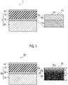
- FIG. 1 is a cross-sectional view illustrating layer configurations of a piezoelectric laminate 5 and a piezoelectric element 1 having the piezoelectric laminate 5, according to a first embodiment.
- the piezoelectric element 1 has the piezoelectric laminate 5 and an upper electrode layer 18.
- the piezoelectric laminate 5 has a substrate 10, and a lower electrode layer 12 and a piezoelectric film 15 which are laminated on the substrate 10.
- “lower” and “upper” do not respectively mean top and bottom in the vertical direction.
- an electrode arranged on the side of the substrate 10 with the piezoelectric film 15 being interposed is merely referred to as the lower electrode layer 12, and an electrode arranged on the side of the piezoelectric film 15 opposite to the substrate 10 is merely referred to as the upper electrode layer 18.
- the lower electrode layer 12 includes a metal layer 12c containing Ni and a surface layer 12b containing a Ni oxide or a Ni oxynitride.
- the surface layer 12b is arranged on the side closest to the piezoelectric film 15.
- the surface layer 12b and the piezoelectric film 15 are formed to be in contact with each other, and a Ni oxide or a Ni oxynitride is present at the boundary 12a therebetween.
- the "metal layer” refers to a layer that consists of only metal species excluding unavoidable impurities, and specifically, it is a layer in which 95 at% or more of the constituent elements are metal elements.
- the "metal layer containing Ni” means that the metal layer contains the Ni element as the main component of the metal layer 12c. It is noted that the main component means a component having 50 at% or more. Further, also in the surface layer 12b containing a Ni oxide or a Ni oxynitride, the main component of the metal species among the elements constituting the surface layer 12b is the Ni element.
- the metal species other than the Ni contained in the lower electrode layer 12 include Cu, Al, Ti, Ta, Cr, and Fe. However, in a case where the metal species contained in the lower electrode layer 12 is only Ni element, the number of material species can be reduced and the manufacturing method can be simplified, which is preferable.
- the surface layer 12b also contains Ni as the main component of the metal species. However, the entire Ni may be oxidized or nitrided, or Ni which is not oxidized and nitrided, a Ni oxide, and a Ni oxynitride may be in a state of being mixed. However, it is preferable that 20 at% or more of the Ni present at the surface layer 12b is nitrided or oxynitrided, and it is more preferable that 30 at% or more thereof is nitrided or oxynitrided.
- the thickness t of the lower electrode layer 12 is preferably about 50 nm to 300 nm and more preferably 100 nm to 300 nm.
- the lower electrode layer 12 preferably a Ni oxide or a Ni oxynitride in a range of 20 nm or more from the side closest to the piezoelectric film 15, and more preferably contains a Ni oxide or a Ni oxynitride in a range of 30 nm or more from the side closest to the piezoelectric film 15.
- the range containing the Ni oxide is preferably 60 nm or less from the side closest to the piezoelectric film 15.
- the thickness t1 of the surface layer 12b is preferably 20 nm to 60 nm and more preferably 40 nm to 60 nm.
- the thickness t2 of the metal layer 12c of the lower electrode layer 12 is preferably 50 nm to 200 nm and more preferably 80 nm to 150 nm. The thickness can be estimated from a scanning electron microscope (SEM) image of a cross section and a transmission electron microscope (TEM) or secondary ion mass spectrometry (SIMS) analysis.
- SEM scanning electron microscope
- TEM transmission electron microscope
- SIMS secondary ion mass spectrometry
- the piezoelectric film 15 contains a perovskite-type oxide. It is preferable that the piezoelectric film 15 is occupied by 80% by mole or more of the perovskite-type oxide. Further, it is preferable that the piezoelectric film 15 is consisting of a perovskite-type oxide (however, it contains unavoidable impurities).
- the perovskite-type oxide is represented by the general formula ABO 3 .
- the piezoelectric film 15 contains Pb as the main component of the A site.
- the main component means a component of which the occupation is 50% by mole or more. That is, "contains Pb as the main component of the A site” means that the component having 50% by mole or more among the A site elements is Pb.
- the elements in the A site other than Pb and the elements of the B site are not particularly limited.
- the perovskite-type oxide is preferably a lead zirconate titanate (PZT) type that contains lead (Pb), zirconium (Zr), titanium (Ti), and oxygen (O).
- PZT lead zirconate titanate
- the perovskite-type oxide is a compound represented by General Formula (P), which contains an additive B1 in the B site of PZT.
- 0 ⁇ x ⁇ 1 and 0 ⁇ y ⁇ 0.3 are satisfied.
- Pb: ⁇ (Zr x Ti 1+x ) 1-y B y ⁇ :O in General Formula (P) a reference ratio thereof is 1:1:3; however, it suffices that the ratio is in a range in which a perovskite structure is obtained.
- B1 examples include scandium (Sc), V, Nb, Ta, Cr, Mo, W, Mn, Fe, Ru, Co, Ir, Ni, Cu, Zn, Ga, In, Sn, and Sb. It is preferable to contain one or more elements among these elements. B1 is more preferably any one of Sc, Nb, or Ni.
- B1 is Nb and that the perovskite-type oxide contains Nb.
- a compound represented by General Formula (1) is particularly preferable. Pb ⁇ (Zr x Ti 1-x ) y-1 Nb y ⁇ O 3 (1) 0 ⁇ x ⁇ 1 , 0.1 ⁇ y ⁇ 0.4 .
- the film thickness of the piezoelectric film 15 is not particularly limited, and it is generally 200 nm or more, for example, 0.2 ⁇ m to 5 ⁇ m.
- the film thickness of the piezoelectric film 15 is preferably 1 ⁇ m or more.
- the substrate 10 is not particularly limited, and examples thereof include substrates such as silicon, glass, stainless steel, yttrium-stabilized zirconia, alumina, sapphire, and silicon carbide.
- substrates such as silicon, glass, stainless steel, yttrium-stabilized zirconia, alumina, sapphire, and silicon carbide.
- a laminated substrate having a SiO 2 oxide film formed on the surface of the silicon substrate may be used.
- the upper electrode layer 18 is paired with the lower electrode layer 12 and is an electrode for applying a voltage to the piezoelectric film 15.
- the main component of the upper electrode layer 18 is not particularly limited, and examples thereof include metals such as gold (Au), platinum (Pt), iridium (Ir), ruthenium (Ru), titanium (Ti), molybdenum (Mo), tantalum (Ta), aluminum (Al), copper (Cu), silver (Ag), chromium (Cr), such as zinc (Zr), and metal oxides thereof, as well as combinations thereof.
- indium tin oxide (ITO), IGZO, LaNiO 3 , SRO (which may contain Ba), or the like may be used.
- the upper electrode layer 18 may be a single layer or may have a laminated structure composed of a plurality of layers. It is noted that from the viewpoint of suppressing oxygen diffusion from the piezoelectric film 15, at least a region of the upper electrode layer 18, which is in contact with the piezoelectric film, is preferably an oxide electrode.
- the layer thickness of the upper electrode layer 18 is not particularly limited, and it is preferably about 50 nm to 300 nm and more preferably 100 nm to 300 nm.
- the lower electrode layer 12 includes the metal layer 12c containing Ni and the surface layer 12b containing a Ni oxide or a Ni oxynitride, and in the lower electrode layer 12, the surface layer 12b is arranged on the side closest to the piezoelectric film 15.
- the region in the lower electrode layer 12 on the side closest to the piezoelectric film 15 is a metal layer, oxygen in the piezoelectric film 15 may leak and migrate to the side of the lower electrode layer 12. The leakage of oxygen in the piezoelectric film 15 leads to the deterioration of piezoelectric characteristics and the deterioration of long-term reliability (durability).
- the surface layer 12b containing a Ni oxide or a Ni oxynitride is arranged on the side closest to the piezoelectric film 15, and thus the oxygen leakage in the piezoelectric film 15 can be suppressed. As a result, it is possible to suppress the deterioration of piezoelectric characteristics and the deterioration of long-term reliability.
- Ni is used as a metal species in the constituent elements of the lower electrode layer 12, and thus the manufacturing cost can be significantly reduced as compared with the piezoelectric element in the related art, in which a metal of the Pt group has been used as the main component.
- the adhesiveness to the substrate is low, and thus in practical use, an intimate attachment layer such as TiW is essential before forming a film of Ir on the substrate.
- an intimate attachment layer such as TiW is essential before forming a film of Ir on the substrate.
- the Ni metal layer 12c is provided in the lower electrode layer 12 on the side of the substrate 10 as in the present embodiment, sufficient adhesiveness can be ensured even in a case where the intimate attachment layer is not provided. That is, in a case where a configuration in which the Ni metal layer 12c is in contact with the substrate is adopted, the intimate attachment layer is unnecessary, and thus the manufacturing cost can be further suppressed.
- the thickness of the surface layer 22b of the lower electrode layer 12 is 20 nm to 60 nm, the effect of suppressing the generation of the oxygen defect in the piezoelectric film 15 is further enhanced, and the deterioration of piezoelectric characteristics and the deterioration of long-term reliability can be further suppressed.
- FIG. 2 is a cross-sectional schematic view illustrating a piezoelectric laminate 5A and a piezoelectric element 1A having the piezoelectric laminate 5A, according to a second embodiment.
- the same reference numerals are respectively assigned to the same constituent elements as those of the piezoelectric laminate 5 and the piezoelectric element 1 according to the first embodiment shown in Fig. 1 , and the detailed description thereof will be omitted.
- the configuration of the lower electrode layer 22 is different from the lower electrode layer 12 in the piezoelectric laminate 5 and the piezoelectric element 1 according to the first embodiment.
- the content of the Ni element changes in an increasing trend from the side closest to the piezoelectric film 15 toward the metal layer 22c in the thickness direction of the surface layer 22b, and the change in the content of the Ni element in the thickness direction is continuous. Further, the change in the content from the surface layer 22b to the metal layer 22c is continuous.
- the content of the Ni element in the thickness direction is a proportion of the Ni element with respect to all elements at each position in the thickness direction, and it is indicated in the unit of at%.
- the "thickness direction” is a direction perpendicular to the substrate 10.
- the change in the content is continuous means that there are no discontinuous portions in the content profile in the thickness direction (see Fig. 2 ).
- the content of the element which constitutes the lower electrode layer 22 and of which the content is 10 at% or more in the entire region of the lower electrode layer 22 is constant or continuously changes in the thickness direction.
- the enlarged view in Fig. 2 schematically illustrates the change in the content of the Ni element in the lower electrode layer 22.
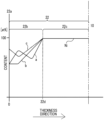
- Fig. 3 illustrates the change (the content profile) in the content of each of the Ni element and the O element, contained in the lower electrode layer 22 in the thickness direction.
- the horizontal axis indicates the position of the lower electrode layer 22 in the thickness direction. 0 on the horizontal axis is the position (a boundary 22a) in the lower electrode layer 22 on the side closest to the piezoelectric film 15, and the two-dot chain line position is the boundary with respect to the substrate 10.
- the lower electrode layer 22 contains the Ni element over the entire region in the thickness direction.
- the content of the Ni element changes in an increasing trend from the boundary 22a with respect to the piezoelectric film 15, which is on the side closest to the piezoelectric film 15, toward the metal layer 22c.
- the content of the Ni element from the surface layer 22b to the metal layer 22c changes continuously. More specifically, the content of the Ni element monotonically increases from the side closest to the piezoelectric film 15 (the boundary 22a) of the surface layer 22b to the metal layer 22c of the surface layer 22b, and the content of the Ni element increases until it reaches the content of the Ni element of the metal layer 22c.
- the content of the Ni element is substantially constant in the metal layer 22c in the thickness direction, and it exhibits substantially 100 at%.
- the increasing trend indicates that in a case where a start point and an end point are compared, the content of the end point is larger than that of the start point, and thus the content tends to increase as a whole.
- the side on the left is denoted by the side of the piezoelectric film 15 and the side on the right is denoted by the side of the substrate 10
- in a case where the content decreases to cause a portion where the measurement error is exceeded even such a case is also included in the increasing trend as long as the content is on the rise as a whole.
- “monotonically increases” means that the content increases without including a case where the content decreases to cause a portion where the measurement error is exceeded in the content profile.
- the preferred ranges of the thicknesses of the lower electrode layer 12, the surface layer 22b, and the metal layer 22c in the present embodiment are respectively the same as the preferred ranges of the thickness t of the lower electrode layer 12, the thickness t1 of the surface layer 12b, and the thickness t2 of the metal layer 12c in the first embodiment described above.
- the boundary 22d between the surface layer 22b and the metal layer 22c, in the lower electrode layer 22 is not clear, for example, in an electron microscopic image.
- the respective thicknesses t1 and t2 of the surface layer 22b and the metal layer 22c are determined from the composition distribution in the thickness direction of the lower electrode layer 22, that is, from the measurement data of the content change of the constituent elements (see Figs. 3 and 6 ). Specifically, in the profile shown in Fig. 3 or Fig. 6 , the region where the O element (or the O element and the N element) exhibits a constant value of the lowest value (almost 0 at%) is regarded as the metal layer 22c.
- the content of the element in the lower electrode layer 22 and the change in the content of the element in the thickness direction can be measured by the secondary ion mass spectrometry (SIMS) analysis.
- SIMS secondary ion mass spectrometry
- the content of the element is a value measured according to SIMS. Further, since the content fluctuates by about ⁇ 5 at% due to noise in the actual measurement data, the fluctuation of about ⁇ 5 at% is regarded as the range of measurement error.
- the lower electrode layer 22 is composed of Ni and oxygen (O) (however, it contains unavoidable impurities), and in the thickness direction of the surface layer 22b of the lower electrode layer 22, the profile that shows the change in the content of the O element is symmetrical with the profile that shows the change in the content of the Ni element, with the line of the content of 50 at% being as the axis of symmetry. That is, the content of the N element continuously decreases from the boundary 22a, which is on the side closest to the piezoelectric film 15, toward the side of the metal layer 22c, and then exhibits a constant value of almost 0 at%.
- O Ni and oxygen
- the profile of the total content of the content of the O element and the content of the N element is the same as the profile of the O element shown in Fig. 3 .
- the oxidized Ni or nitrided Ni may be mixed with the oxidized or oxynitrided Ni.
- the Ni element is nitrided or oxynitrided, and it is more preferable that 30 at% or more thereof is nitrided or oxynitrided.
- the lower electrode layer 22 includes the metal layer 22c containing a Ni element and the surface layer 22b containing a Ni oxide or a Ni oxynitride, and in the electrode layer 22, the surface layer 22b is arranged on the side closest to the piezoelectric film 15. For this reason, it is possible to suppress the oxygen in the piezoelectric film 15, and as a result, it is possible to suppress the deterioration of piezoelectric characteristics and the deterioration of long-term reliability.
- Ni is used as a metal species of the lower electrode layer 22, and thus the manufacturing cost can be significantly reduced as compared with the piezoelectric element in the related art, in which a metal of the Pt group has been used as the main component.
- the content of the Ni element of the lower electrode layer 22 changes in an increasing trend from the side closest to the piezoelectric film 15 to the metal layer 22c in the thickness direction of the surface layer 22b, and the change of the content is continuous. Further, the change in the content from the surface layer 22b to the metal layer 22c is continuous. In a case where the change in the content of the Ni element in the thickness direction is discontinuous, the adhesiveness may be deteriorated at the discontinuous portion, whereby peeling may occur.
- the occurrence of peeling can be suppressed.
- the effect of suppressing the generation of the oxygen defect in the piezoelectric film 15 can be enhanced, and the effect of suppressing the deterioration of conductivity can be suppressed.
- the change in the content of the Ni element in the thickness direction of the lower electrode layer 22 is as shown in Fig. 3 .
- the change in the content of the Ni element in the thickness direction of the lower electrode layer 22 is not limited to that shown in Fig. 3 .
- Fig. 4 shows other examples (profiles a to c) of the change in the content of the Ni element in the lower electrode layer 22 in the thickness direction of the surface layer 22b.
- the horizontal axis indicates the position of the lower electrode layer 22 in the thickness direction. 0 on the horizontal axis is the position (a boundary 22a) in the lower electrode layer 22 on the side closest to the piezoelectric film 15, and the two-dot chain line position is the boundary with respect to the substrate 10.
- the respective profiles of the O element are, for example, symmetrical with the profile of the Ni element, with the line of the content of 50 at% being as the central axis.
- the content of the Ni element in the thickness direction of the surface layer 22b is about 50 at% at the boundary 22a with respect to the piezoelectric film 15, and it gradually increases toward the side of the metal layer 22c to take the maximum value. Then, it may decrease once and further increase to match the content in the metal layer 22c at the boundary of the metal layer 22c.
- the profile a has a high Ni element content at the boundary 22d (the end point) with respect to the metal layer 22c as compared with the boundary 22a (the start point) with respect to the piezoelectric film 15, and thus it can be said that the content changes in an increasing trend from the side of the piezoelectric film 15 toward the metal layer 22c.
- the content of the Ni element in the thickness direction of the surface layer 22b is about 50 at% at the boundary 22a with respect to the piezoelectric film 15, and it exhibits a constant value for a while from the boundary 22a toward the metal layer 22c. Then, it may monotonically increase to match the content in the metal layer 22c at the boundary of the metal layer 22c.
- the content of the Ni element is substantially 50 at% in the lower electrode layer 22 on the side closest to the piezoelectric film 15.
- the content of the Ni element is 50 at%
- the content of the O element is 50 at% in a case where the Ni element is completely nitrided at the boundary 22a on the side of the piezoelectric film 15.
- the non-oxidized Ni element is not present, and thus the effect of suppressing the generation of oxygen defect in the piezoelectric film 15 is high.
- the content of the Ni element at the boundary 22a in the lower electrode layer 22 on the side closest to the piezoelectric film 15 is not limited to 50 at%, and it may be larger than 50 at%. Further, as shown in the profile c of Fig. 4 , the content once decreases from the side closest to the piezoelectric film 15 toward the metal layer 22c to a content lower than the content of the Ni element at the boundary 22a. Then, it may increase to match the content in the metal layer 22c at the boundary of the metal layer 22c.
- the lower electrode layer 22 has the metal layer 22c containing a Ni element and the surface layer 22b containing a Ni nitride, and the surface layer 22b is arranged on the side closest to the piezoelectric film 15.
- the surface layer 22b is arranged on the side closest to the piezoelectric film 15.
- the content of the Ni element in the lower electrode layer 22 changes in an increasing trend from the side closest to the piezoelectric film 15 to the metal layer 22c in the thickness direction of the surface layer 22b, the change thereof in the content is continuous, and the change in the content of the Ni element from the surface layer 22b to the metal layer 22c is continuous.
- the occurrence of peeling can be suppressed, the effect of suppressing the generation of oxygen defect in the piezoelectric film 15 can be enhanced, and the effect of suppressing the deterioration of conductivity can be suppressed.
- the content of the Ni element in the metal layer 12c or 22c has been described as being constant in the thickness direction. However, it is noted that the content of the Ni element in the metal layer 12c or 22c in the thickness direction. In this case, the content of metal species other than the Ni element increases or decreases in association with the change in the content of the Ni element.
- FIG. 5 is a cross-sectional schematic view illustrating a piezoelectric laminate 5B and a piezoelectric element 1B having the piezoelectric laminate 5B, according to a second embodiment.
- the same reference numerals are respectively assigned to the same constituent elements as those of the piezoelectric laminates 5 and 5A and the piezoelectric elements 1 and 1A according to the first embodiment and the second embodiment shown in Fig. 1 and Fig. 2 , and detailed description thereof will be omitted.
- the piezoelectric laminate 5B and the piezoelectric element 1B have an intimate attachment layer 11 between the substrate 10 and the lower electrode layer 22. Further, an alignment control layer 13 is provided between the lower electrode layer 22 and the piezoelectric film 15.
- the intimate attachment layer 11 is provided for improving the adhesiveness between the substrate 10 and the lower electrode layer 22 and suppressing peeling.
- Ti, W, TiW, or the like is preferably used for the intimate attachment layer 11.
- the alignment control layer 13 is formed on the lower electrode layer 22.
- the alignment control layer 13 is a layer provided for suppressing the generation of a pyrochlore phase that is easily formed at the initial stage of film formation of the piezoelectric film 15 and obtaining a good perovskite-type oxide.
- the alignment control layer 13 contains a metal oxide different from the Ni oxide.
- the metal oxide preferably contains at least one of Sr or Ba.
- the alignment control layer 13 it is preferable to use, for example, the growth control layer described in WO2020/250591A , WO2020/250632A , JP2020-202327A , or the like.
- the alignment control layer 13 preferably contains a metal oxide represented by General Formula (2).
- Specific examples of the substance of the alignment control layer 13 include BaRuO 3 and SrRuO 3 .
- the thickness of the alignment control layer 13 is preferably 2 nm or more and 20 nm or less and more preferably about 10 nm.
- the lower electrode layer 22 includes the metal layer 22c containing a Ni element and the surface layer 22b containing a Ni oxide or a Ni oxynitride, and in the electrode layer 22, the surface layer 22b is arranged on the side closest to the piezoelectric film 15. For this reason, it is possible to suppress the oxygen in the piezoelectric film 15, and as a result, it is possible to suppress the deterioration of piezoelectric characteristics and the deterioration of long-term reliability. Further, Ni is used as a metal species of the lower electrode layer 22, and thus the manufacturing cost can be significantly reduced as compared with the piezoelectric element in the related art, in which a metal of the Pt group has been used as the main component.
- the configuration of the lower electrode layer 22 is the same as that in the piezoelectric laminate 5A and the piezoelectric element 1A according to the second embodiment.
- the change in the content of the Ni element in the lower electrode layer 22 continuous, and thus the occurrence of peeling can be suppressed.
- the content of the Ni element is in an increasing trend from the side of the piezoelectric film 15 toward the substrate 10, the effect of suppressing the generation of the oxygen defect in the piezoelectric film 15 can be enhanced, and the effect of suppressing the deterioration of conductivity can be suppressed.
- the content of the Ni element monotonically increases from the side of the piezoelectric film 15, it is possible to further enhance the effect of suppressing the generation of oxygen defect in the piezoelectric film 15 and the effect of suppressing the deterioration of conductivity.
- the piezoelectric laminate 5B and the piezoelectric element 1B according to the present embodiment have the alignment control layer 13, and the piezoelectric film 15 is formed on the alignment control layer 13.
- the piezoelectric film 15 is formed on the alignment control layer 13.
- the piezoelectric elements 1,1A, and 1B or the piezoelectric laminates 5, 5A, and 5B according to each of the above embodiments can be applied to an ultrasonic device, a mirror device, a sensor, a memory, and the like.
- a 6-inch Si wafer attached with a thermal oxide film was used as the substrate.
- a lower electrode layer was formed on the thermal oxide film of the substrate.
- the film formation conditions for the lower electrode layer in each example were as follows.
- a film of 20 nm of TiW was formed on the thermal oxide film of the substrate as an intimate attachment layer.
- a film of 150 nm of Ir was formed on the TiW layer as the lower electrode layer under the conditions of an Ar gas of 60 sccm, an RF electric power of 300 W, and a film formation pressure of 0.25 Pa.
- the substrate temperature at the time of film formation of the TiW layer and the Ir layer was set to 350°C.
- a film of 150 nm of Ni was formed as the lower electrode layer under the conditions of an Ar gas of 60 sccm, an RF electric power of 300 W, a film formation pressure of 0.25 Pa, and a substrate temperature of 350°C.
- a film of 100 nm of Ni was formed as the metal layer under the conditions of an Ar gas of 60 sccm, an RF electric power of 300 W, a film formation pressure of 0.25 Pa, and a substrate temperature of 350°C. Subsequently, a film of 50 nm of a Ni oxide (NiO) was formed, as the surface layer, on the Ni layer under the conditions of an Ar gas of 30 sccm, an O 2 gas of 30 sccm, an RF electric power of 500 W, and a film formation pressure of 0.25 Pa.
- NiO Ni oxide
- the lower electrode layer had a two-layer structure consisting of a metal layer consisting of a Ni layer and a surface layer consisting of a NiO layer provided on an upper layer of the metal layer.
- Table 1 in the item of the layer configuration of the lower electrode layer, the description is made in the order of the surface layer / the metal layer.
- a film of 100 nm of Ni was formed as the metal layer under the conditions of an Ar gas of 60 sccm, an RF electric power of 300 W, a film formation pressure of 0.25 Pa, and a substrate temperature of 350°C. Subsequently, for each example, a film of 50 nm of a Ni oxide was formed on the Ni layer to form a surface layer under the conditions of an RF electric power of 500 W and a film formation pressure of 0.25 Pa, while gradually reducing the Ar gas from 60 sccm to 30 sccm and at the same time gradually increasing the O 2 gas from 0 sccm to 30 sccm.
- the lower electrode layer had a laminated structure of a metal layer consisting of a Ni layer and a Ni oxide layer consisting of a composition gradient layer in which the content of the Ni element and the content of the O element gradually change, where the Ni oxide layer had been provided on an upper layer of the metal layer.
- NiO grade, 50 nm indicates that the Ni oxide layer is a composition gradient layer having a thickness of 50 nm.
- the content of the Ni element changed continuously between the metal layer and the surface layer and in the surface layer, and thus a seamless lower electrode layer was obtained.
- a film of 100 nm of Ni was formed as the metal layer under the conditions of an Ar gas of 60 sccm, an RF electric power of 300 W, a film formation pressure of 0.25 Pa, and a substrate temperature of 350°C. Subsequently, for each example, a film of 50 nm of a Ni oxynitride was formed on the Ni layer to form a surface layer under the conditions of an RF electric power of 500 W and a film formation pressure of 0.25 Pa, while gradually reducing the Ar gas from 60 sccm to 30 sccm and at the same time gradually increasing each of the O 2 gas and the N 2 gas from 0 sccm to 15 sccm.
- the lower electrode layer had a laminated structure of a metal layer consisting of a Ni layer and a Ni oxide layer consisting of a gradient layer in which the content of the Ni element gradually changes, where the Ni oxynitride layer had been provided on an upper layer of the metal layer.
- NiON (gradient, 50 nm) indicates that the Ni oxynitride layer is a composition gradient layer having a thickness of 50 nm.
- the content of the Ni element changed continuously between the metal layer and the surface layer and in the surface layer, and thus a seamless lower electrode layer was obtained.
- Example 4 Ar was allowed to flow on the lower electrode layer so that the substrate temperature was 500°C and the film formation pressure was 0.8 Pa, and then a film of 10 nm of BaRuO 3 was formed as the alignment control layer.
- Example 5 Ar was allowed to flow on the lower electrode layer so that the substrate temperature was 500°C and the film formation pressure was 0.8 Pa, and then a film of 10 nm of SrRuO 3 was formed as the alignment control layer.
- the alignment control layer is not provided in other examples and the comparative examples.
- N-PZT Nb-doped PZT
- a sintered body of Pb 1.15 (Zr 0.46 Ti 0.42 Nb 0.12 )O 3 having a diameter of 120 mm was used as a target material.
- the film formation was carried out under the same film formation conditions as in Example 1 except that the substrate temperature was set to 550°C.
- a target material of Pb 1.3 (Zr 0.325 Ti 0.285 Nb 0.3 Ni 0.09 )O 3 was used.
- the film formation conditions were the same as in Example 1.
- a target material of Pb 1.3 (Zr 0.4125 Ti 0.3725 Nb 0.2 Sc 0.015 )O 3 was used.
- the film formation conditions were the same as in Example 1.
- a laminated substrate in which a lower electrode and a piezoelectric film were laminated on the substrate was obtained as described above. It is noted that regarding the laminated substrates of each example and comparative example, a diffraction pattern due to X-ray diffraction was acquired by an X-ray diffractometer manufactured by Malvern Panalytical, whereby it was confirmed that the piezoelectric film has a perovskite type structure.
- the element distribution in the thickness direction of the lower electrode layer can be measured according to a secondary ion mass spectrometry (SIMS) analysis.
- SIMS secondary ion mass spectrometry
- the data obtained according to the SIMS analysis using a sample having the lower electrode layer of Example 2 is shown in Fig. 6 .
- the sample was irradiated with an Ar + ion, and the analysis was carried out while cutting the sample from the surface side of the Ni oxide layer.
- the horizontal axis is the position in the thickness direction of the lower electrode layer
- 0 is the surface position of the lower electrode layer
- the closer to the side on the right of the horizontal axis is, the closer to the substrate is.
- the contents of both Ni element and O element were in the vicinity of 50 at%.
- the content of the Ni element gradually increased from the surface toward the side of the substrate and reached substantially 100 at% at about 50 nm, exhibiting a constant value.
- the content of the N element gradually decreased from the surface toward the side of the substrate and reached substantially 0 at% at about 50 nm, exhibiting a constant value.
- the laminated substrate was subjected to dicing processing to a size of an one-inch (25 mm) square to produce a piezoelectric laminate of an one-inch square.
- An ITO layer having a thickness of 100nm was formed by sputtering in a state where a metal mask having a circular opening having a diameter of 400 ⁇ m was arranged on the piezoelectric film.
- a sample for measuring the dielectric constant having a size of 1 inch square and having a circular upper electrode layer having a diameter of 400 ⁇ m at the center of the surface of the piezoelectric film, was obtained.
- Comparative Example 1 is a piezoelectric element having a lower electrode layer consisting of Ir, which has been used in the related art, and it is an example in which the dielectric constant is good.
- Table 1 the ratio of the dielectric constant for each Example and Comparative Example to that of Comparative Example is shown together.
- the sample prepared for measuring the dielectric constant was used.
- the lower electrode layer was grounded, a voltage of -30 V was applied to the upper electrode layer, and the time (hr) taken from the start of the voltage application to the occurrence of dielectric breakdown was measured.
- the measurement results are shown in Table 1. Here, it is regarded that dielectric breakdown has occurred at the time in a case where a current of 1 mA or more has flowed through the piezoelectric element.
- the dielectric constant is relatively high, which is favorable; however, the durability is low and the long-term reliability is lacking.
- the lower electrode layer consisting of a Ni layer is provided as in Comparative Example 2 gives such results that the dielectric constant is low by 10% or more lower as compared with Comparative Example 1 having an Ir layer as the lower electrode layer, and thus it is revealed that the piezoelectric characteristics are low as compared with the element in the related art.
- Example 1 has, as the lower electrode layer, a metal layer consisting of Ni and a surface layer consisting of a Ni oxide of which the composition does not change in the thickness direction. In this configuration, the results were such that the dielectric constant was high and the durability was significantly high as compared with Comparative Example 1.
- Example 1 the dielectric constant is high or is reduced by only 4% or less as compared with Comparative Example, and thus good piezoelectric characteristics are provided.
- Example 1 to 7 the durability significantly improved as compared with Comparative Example 1.
- Example 1 the durability is slightly inferior to Examples 2 to 7. It is conceived that in Examples 2 to 7, the composition change in the lower electrode layer is continuous, and thus peeling is difficult to occur as compared with Example 1, whereby the durability is further improved.
- the piezoelectric elements of Examples 4 and 5 having the alignment control layer have a dielectric constant comparable to those of the case where the Ir electrode layer is provided, and they have a great effect of improving durability.
- the results obtained from Examples 2 and 3 were such that the effect of improving the piezoelectricity and the effect of improving durability are high in a case where the surface layer of the lower electrode layer is a NiO gradient layer as compared with a case where it is a NiON gradient layer.
- Examples 1 to 7 only Ni is used as the metal species in the lower electrode layer, and thus the material cost can be significantly suppressed as compared with a case where Ir is used. It is revealed that as shown in Examples 1 to 7, according to the present disclosed technology, it is possible to provide a piezoelectric element that exhibits piezoelectric characteristics comparable to those of the piezoelectric element in the related art using Ir in the lower electrode layer and has high reliability, and with which the manufacturing cost can be significantly reduced.
Landscapes
- Chemical & Material Sciences (AREA)
- Engineering & Computer Science (AREA)
- Materials Engineering (AREA)
- Ceramic Engineering (AREA)
- Physical Vapour Deposition (AREA)
- Transducers For Ultrasonic Waves (AREA)
- Compositions Of Oxide Ceramics (AREA)
- Piezo-Electric Or Mechanical Vibrators, Or Delay Or Filter Circuits (AREA)
- Particle Formation And Scattering Control In Inkjet Printers (AREA)
Abstract
Description
- The present disclosure relates to a piezoelectric laminate and a piezoelectric element.
- As a material having excellent piezoelectricity and excellent ferroelectricity, there is known a perovskite-type oxide such as lead zirconate titanate (Pb(Zr,Ti)O3, hereinafter referred to as PZT). A piezoelectric body consisting of a perovskite-type oxide is applied as a piezoelectric film in a piezoelectric element having a lower electrode, a piezoelectric film, and an upper electrode on a substrate. This piezoelectric element has been developed into various devices such as a memory, an inkjet head (an actuator), a micromirror device, an angular velocity sensor, a gyro sensor, a piezoelectric micromachined ultrasonic transducer (PMUT), and an oscillation power generation device.
- The piezoelectric characteristics greatly change due to the excess or deficiency of oxygen in the perovskite structure of the perovskite-type oxide. In particular, in a perovskite-type oxide containing Pb such as a PZT film, oxygen is easily eliminated, and the oxygen defect in the piezoelectric film easily causes the deterioration of piezoelectric characteristics and the deterioration of durability. In order to suppress the oxygen elimination in the perovskite-type oxide, it is effective to use a conductive oxide such as SRO (SrRuO3) or IrO2 in regions of the lower electrode and the upper electrode, where these regions are in contact with the piezoelectric film. Further, in a case where a conductive oxide is used in the region in contact with the piezoelectric film, an electrode layer consisting of a layer of a noble metal such as Pt or Ir is generally laminated on the conductive oxide layer in order to ensure good conductivity (see, for example,
JP2018-085478A -
JP2007-300071A - As described in
JP2018-085478A JP2018-085478A JP2007-300071A - However, since a metal of the platinum group is very expensive, there is a problem that it is not possible to sufficiently suppress the manufacturing cost of a piezoelectric element having an electrode containing the platinum group.
- The present disclosed technology has been made in consideration of the above circumstances, and an object of the present disclosed technology is to provide a piezoelectric laminate and a piezoelectric element, which makes it possible to suppress the deterioration of piezoelectric characteristics and suppress the manufacturing cost.
- The piezoelectric laminate of the present disclosure is a piezoelectric laminate comprising, on a substrate in the following order:
- a lower electrode layer; and
- a piezoelectric film containing a perovskite-type oxide,
- in which the lower electrode layer includes a metal layer containing Ni and a surface layer containing a Ni oxide or a Ni oxynitride, and
- in the lower electrode layer, the surface layer is arranged on the side closest to the piezoelectric film.
- In the piezoelectric laminate of the present disclosure, it is preferable that in a thickness direction of the surface layer, a content of a Ni element changes in an increasing trend from the side closest to the piezoelectric film to the metal layer, the change in the content of the Ni element is continuous, and the change in the content of the Ni element from the surface layer to the metal layer is continuous.
- In the piezoelectric laminate of the present disclosure, it is preferable that the thickness of the surface layer is 20 nm to 60 nm.
- In the piezoelectric laminate of the present disclosure, it is preferable that an alignment control layer containing a metal oxide different from the Ni oxide is provided between the lower electrode layer and the piezoelectric film. Here, the metal oxide preferably contains at least one of Sr or Ba.
- In the piezoelectric laminate of the present disclosure, it is preferable that the perovskite-type oxide contains Pb, Zr, Ti, and O.
- In the piezoelectric laminate of the present disclosure, it is preferable that the perovskite-type oxide contains at least one of Nb, Sc, or Ni.
- In the piezoelectric laminate of the present disclosure, it is preferable that the perovskite-type oxide is a compound represented by General Formula (1),
Pb{(ZrxTi1-x)y-1Nby}O3 (1)
0 < x <1, 0.1 ≤ y ≤ 0.4. - The piezoelectric element of the present disclosure has the piezoelectric laminate of the present disclosure and an upper electrode layer provided on the piezoelectric film of the piezoelectric laminate.
- According to the piezoelectric laminate and the piezoelectric element of the present disclosure, it is possible to provide a piezoelectric laminate and a piezoelectric element, which makes it possible to suppress the deterioration of piezoelectric characteristics and suppress the manufacturing cost.
-
-
Fig. 1 is a cross-sectional view illustrating a layer configuration of a piezoelectric laminate and a piezoelectric element, according to a first embodiment. -
Fig. 2 is a cross-sectional view illustrating a layer configuration of a piezoelectric laminate and a piezoelectric element according to a second embodiment. -
Fig. 3 is a graph showing profiles of contents of a Ni element and an O element in a thickness direction of a lower electrode layer in the piezoelectric element illustrated inFig. 2 . -
Fig. 4 is a graph showing another profile of the contents of the Ni element in a thickness direction of a lower electrode layer in the piezoelectric element illustrated inFig. 2 . -
Fig. 5 is a cross-sectional view illustrating a layer configuration of a piezoelectric laminate and a piezoelectric element according to a third embodiment. -
Fig. 6 is a graph showing profiles of contents of a Ni element and an O element in a thickness direction of a lower electrode layer in the piezoelectric element of Example 2. - Hereinafter, embodiments of the present invention will be described with reference to the drawings. In the drawings below, the layer thickness of each of the layers and the ratio therebetween are appropriately changed and drawn for easy visibility, and thus they do not necessarily reflect the actual layer thickness and ratio.
- Piezoelectric laminate 5 and piezoelectric element 1, according to first embodimentFig. 1 is a cross-sectional view illustrating layer configurations of a piezoelectric laminate 5 and a piezoelectric element 1 having the piezoelectric laminate 5, according to a first embodiment. As illustrated in
Fig. 1 , the piezoelectric element 1 has the piezoelectric laminate 5 and anupper electrode layer 18. The piezoelectric laminate 5 has asubstrate 10, and alower electrode layer 12 and apiezoelectric film 15 which are laminated on thesubstrate 10. Here, "lower" and "upper" do not respectively mean top and bottom in the vertical direction. As result, an electrode arranged on the side of thesubstrate 10 with thepiezoelectric film 15 being interposed is merely referred to as thelower electrode layer 12, and an electrode arranged on the side of thepiezoelectric film 15 opposite to thesubstrate 10 is merely referred to as theupper electrode layer 18. - In the piezoelectric laminate 5, the
lower electrode layer 12 includes ametal layer 12c containing Ni and asurface layer 12b containing a Ni oxide or a Ni oxynitride. In thelower electrode layer 12, thesurface layer 12b is arranged on the side closest to thepiezoelectric film 15. In this example, thesurface layer 12b and thepiezoelectric film 15 are formed to be in contact with each other, and a Ni oxide or a Ni oxynitride is present at theboundary 12a therebetween. - The "metal layer" refers to a layer that consists of only metal species excluding unavoidable impurities, and specifically, it is a layer in which 95 at% or more of the constituent elements are metal elements. The "metal layer containing Ni" means that the metal layer contains the Ni element as the main component of the
metal layer 12c. It is noted that the main component means a component having 50 at% or more. Further, also in thesurface layer 12b containing a Ni oxide or a Ni oxynitride, the main component of the metal species among the elements constituting thesurface layer 12b is the Ni element. Examples of the metal species other than the Ni contained in thelower electrode layer 12 include Cu, Al, Ti, Ta, Cr, and Fe. However, in a case where the metal species contained in thelower electrode layer 12 is only Ni element, the number of material species can be reduced and the manufacturing method can be simplified, which is preferable. - The
surface layer 12b also contains Ni as the main component of the metal species. However, the entire Ni may be oxidized or nitrided, or Ni which is not oxidized and nitrided, a Ni oxide, and a Ni oxynitride may be in a state of being mixed. However, it is preferable that 20 at% or more of the Ni present at thesurface layer 12b is nitrided or oxynitrided, and it is more preferable that 30 at% or more thereof is nitrided or oxynitrided. - The thickness t of the
lower electrode layer 12 is preferably about 50 nm to 300 nm and more preferably 100 nm to 300 nm. Thelower electrode layer 12 preferably a Ni oxide or a Ni oxynitride in a range of 20 nm or more from the side closest to thepiezoelectric film 15, and more preferably contains a Ni oxide or a Ni oxynitride in a range of 30 nm or more from the side closest to thepiezoelectric film 15. In order to ensure sufficient conductivity without the thickness t of thelower electrode layer 12 becoming too thick, the range containing the Ni oxide is preferably 60 nm or less from the side closest to thepiezoelectric film 15. That is, it contains a Ni oxide or a Ni oxynitride preferably over 20 nm to 60 nm, and more preferably 40 nm to 60 nm from the side closest to thepiezoelectric film 15, in thelower electrode layer 12. As a result, the thickness t1 of thesurface layer 12b is preferably 20 nm to 60 nm and more preferably 40 nm to 60 nm. In addition, the thickness t2 of themetal layer 12c of thelower electrode layer 12 is preferably 50 nm to 200 nm and more preferably 80 nm to 150 nm. The thickness can be estimated from a scanning electron microscope (SEM) image of a cross section and a transmission electron microscope (TEM) or secondary ion mass spectrometry (SIMS) analysis. - The
piezoelectric film 15 contains a perovskite-type oxide. It is preferable that thepiezoelectric film 15 is occupied by 80% by mole or more of the perovskite-type oxide. Further, it is preferable that thepiezoelectric film 15 is consisting of a perovskite-type oxide (however, it contains unavoidable impurities). - The perovskite-type oxide is represented by the general formula ABO3.
- In the general formula, A is an A-site element, which is one of Pb, barium (Ba), lanthanum (La), Sr, bismuth (Bi), lithium (Li), sodium (Na), calcium (Ca), cadmium (Cd), magnesium (Mg), or potassium (K), or a combination of two or more thereof.
- In the general formula, B is a B-site element, which is one of Ti, Zr, vanadium (V), Nb, Ta, chromium (Cr), molybdenum (Mo), tungsten (W), manganese (Mn), iron (Fe), Ru, cobalt (Co), Ir, nickel (Ni), copper (Cu), zinc (Zn), gallium (Ga), In, Sn, antimony (Sb), or a lanthanide element, or a combination of two or more thereof.
- In the general formula, O is oxygen.
- Regarding A:B:O, a reference ratio is 1:1:3; however, it suffices that the ratio is in a range in which a perovskite structure is obtained.
- It is particularly preferable that the
piezoelectric film 15 contains Pb as the main component of the A site. It is noted that in the present specification, "the main component" means a component of which the occupation is 50% by mole or more. That is, "contains Pb as the main component of the A site" means that the component having 50% by mole or more among the A site elements is Pb. In the perovskite-type oxide containing Pb, the elements in the A site other than Pb and the elements of the B site are not particularly limited. - The perovskite-type oxide is preferably a lead zirconate titanate (PZT) type that contains lead (Pb), zirconium (Zr), titanium (Ti), and oxygen (O).
- In particular, it is preferable that the perovskite-type oxide is a compound represented by General Formula (P), which contains an additive B1 in the B site of PZT.
Pb{(ZrxTi1-x)1-yB1y}O3 (P)
Here, 0 < x < 1 and 0 < y < 0.3 are satisfied. It is noted that regarding Pb:{(ZrxTi1+x)1-yBy}:O in General Formula (P), a reference ratio thereof is 1:1:3; however, it suffices that the ratio is in a range in which a perovskite structure is obtained. - Examples of the B1 include scandium (Sc), V, Nb, Ta, Cr, Mo, W, Mn, Fe, Ru, Co, Ir, Ni, Cu, Zn, Ga, In, Sn, and Sb. It is preferable to contain one or more elements among these elements. B1 is more preferably any one of Sc, Nb, or Ni.
- In particular, it is preferable that B1 is Nb and that the perovskite-type oxide contains Nb. A compound represented by General Formula (1) is particularly preferable.
Pb{(ZrxTi1-x)y-1Nby}O3 (1)

- The film thickness of the
piezoelectric film 15 is not particularly limited, and it is generally 200 nm or more, for example, 0.2 µm to 5 µm. The film thickness of thepiezoelectric film 15 is preferably 1 µm or more. - The
substrate 10 is not particularly limited, and examples thereof include substrates such as silicon, glass, stainless steel, yttrium-stabilized zirconia, alumina, sapphire, and silicon carbide. As thesubstrate 10, a laminated substrate having a SiO2 oxide film formed on the surface of the silicon substrate may be used. - The
upper electrode layer 18 is paired with thelower electrode layer 12 and is an electrode for applying a voltage to thepiezoelectric film 15. The main component of theupper electrode layer 18 is not particularly limited, and examples thereof include metals such as gold (Au), platinum (Pt), iridium (Ir), ruthenium (Ru), titanium (Ti), molybdenum (Mo), tantalum (Ta), aluminum (Al), copper (Cu), silver (Ag), chromium (Cr), such as zinc (Zr), and metal oxides thereof, as well as combinations thereof. Further, as theupper electrode layer 18, indium tin oxide (ITO), IGZO, LaNiO3, SRO (which may contain Ba), or the like may be used. Theupper electrode layer 18 may be a single layer or may have a laminated structure composed of a plurality of layers. It is noted that from the viewpoint of suppressing oxygen diffusion from thepiezoelectric film 15, at least a region of theupper electrode layer 18, which is in contact with the piezoelectric film, is preferably an oxide electrode. - The layer thickness of the
upper electrode layer 18 is not particularly limited, and it is preferably about 50 nm to 300 nm and more preferably 100 nm to 300 nm. - As described above, in the piezoelectric laminate 5 and the piezoelectric element 1 according to the present embodiment, the
lower electrode layer 12 includes themetal layer 12c containing Ni and thesurface layer 12b containing a Ni oxide or a Ni oxynitride, and in thelower electrode layer 12, thesurface layer 12b is arranged on the side closest to thepiezoelectric film 15. In a case where the region in thelower electrode layer 12 on the side closest to thepiezoelectric film 15 is a metal layer, oxygen in thepiezoelectric film 15 may leak and migrate to the side of thelower electrode layer 12. The leakage of oxygen in thepiezoelectric film 15 leads to the deterioration of piezoelectric characteristics and the deterioration of long-term reliability (durability). However, in the piezoelectric laminate 5 and the piezoelectric element 1 according to the present embodiment, thesurface layer 12b containing a Ni oxide or a Ni oxynitride is arranged on the side closest to thepiezoelectric film 15, and thus the oxygen leakage in thepiezoelectric film 15 can be suppressed. As a result, it is possible to suppress the deterioration of piezoelectric characteristics and the deterioration of long-term reliability. - Further, Ni is used as a metal species in the constituent elements of the
lower electrode layer 12, and thus the manufacturing cost can be significantly reduced as compared with the piezoelectric element in the related art, in which a metal of the Pt group has been used as the main component. - Further, according to the findings of the inventors of the present invention, in a case where an electrode layer consisting of Ir is used as the lower electrode layer, the adhesiveness to the substrate is low, and thus in practical use, an intimate attachment layer such as TiW is essential before forming a film of Ir on the substrate. However, in a case where the
Ni metal layer 12c is provided in thelower electrode layer 12 on the side of thesubstrate 10 as in the present embodiment, sufficient adhesiveness can be ensured even in a case where the intimate attachment layer is not provided. That is, in a case where a configuration in which theNi metal layer 12c is in contact with the substrate is adopted, the intimate attachment layer is unnecessary, and thus the manufacturing cost can be further suppressed. - In a case where the thickness of the
surface layer 22b of thelower electrode layer 12 is 20 nm to 60 nm, the effect of suppressing the generation of the oxygen defect in thepiezoelectric film 15 is further enhanced, and the deterioration of piezoelectric characteristics and the deterioration of long-term reliability can be further suppressed. - Piezoelectric laminate and piezoelectric element, according to second embodiment
Fig. 2 is a cross-sectional schematic view illustrating apiezoelectric laminate 5A and apiezoelectric element 1A having thepiezoelectric laminate 5A, according to a second embodiment. InFig. 2 , the same reference numerals are respectively assigned to the same constituent elements as those of the piezoelectric laminate 5 and the piezoelectric element 1 according to the first embodiment shown inFig. 1 , and the detailed description thereof will be omitted. - In the
piezoelectric laminate 5A and thepiezoelectric element 1A according to the second embodiment, the configuration of thelower electrode layer 22 is different from thelower electrode layer 12 in the piezoelectric laminate 5 and the piezoelectric element 1 according to the first embodiment. - In the
piezoelectric laminate 5A and thepiezoelectric element 1A according to the present embodiment, the content of the Ni element changes in an increasing trend from the side closest to thepiezoelectric film 15 toward themetal layer 22c in the thickness direction of thesurface layer 22b, and the change in the content of the Ni element in the thickness direction is continuous. Further, the change in the content from thesurface layer 22b to themetal layer 22c is continuous. Here, "the content of the Ni element in the thickness direction" is a proportion of the Ni element with respect to all elements at each position in the thickness direction, and it is indicated in the unit of at%. The "thickness direction" is a direction perpendicular to thesubstrate 10. "The change in the content is continuous" means that there are no discontinuous portions in the content profile in the thickness direction (seeFig. 2 ). In thelower electrode layer 22, it is preferable that among the constituent elements constituting thelower electrode layer 22 other than the Ni element, the content of the element which constitutes thelower electrode layer 22 and of which the content is 10 at% or more in the entire region of thelower electrode layer 22 is constant or continuously changes in the thickness direction. - The enlarged view in
Fig. 2 schematically illustrates the change in the content of the Ni element in thelower electrode layer 22. In the enlarged view inFig. 2 , the larger the content of the Ni element is, the darker the color is, and the smaller the content is, the lighter the color is. Further,Fig. 3 illustrates the change (the content profile) in the content of each of the Ni element and the O element, contained in thelower electrode layer 22 in the thickness direction. The horizontal axis indicates the position of thelower electrode layer 22 in the thickness direction. 0 on the horizontal axis is the position (aboundary 22a) in thelower electrode layer 22 on the side closest to thepiezoelectric film 15, and the two-dot chain line position is the boundary with respect to thesubstrate 10. - As shown in
Fig. 3 , in the present embodiment, thelower electrode layer 22 contains the Ni element over the entire region in the thickness direction. In the thickness direction of thesurface layer 22b, the content of the Ni element changes in an increasing trend from theboundary 22a with respect to thepiezoelectric film 15, which is on the side closest to thepiezoelectric film 15, toward themetal layer 22c. In addition, the content of the Ni element from thesurface layer 22b to themetal layer 22c changes continuously. More specifically, the content of the Ni element monotonically increases from the side closest to the piezoelectric film 15 (theboundary 22a) of thesurface layer 22b to themetal layer 22c of thesurface layer 22b, and the content of the Ni element increases until it reaches the content of the Ni element of themetal layer 22c. In the present embodiment, the content of the Ni element is substantially constant in themetal layer 22c in the thickness direction, and it exhibits substantially 100 at%. Here, the increasing trend indicates that in a case where a start point and an end point are compared, the content of the end point is larger than that of the start point, and thus the content tends to increase as a whole. For example, as inFig. 3 , in the content profile in which the side on the left is denoted by the side of thepiezoelectric film 15 and the side on the right is denoted by the side of thesubstrate 10, in a case where the content decreases to cause a portion where the measurement error is exceeded, even such a case is also included in the increasing trend as long as the content is on the rise as a whole. Further, "monotonically increases" means that the content increases without including a case where the content decreases to cause a portion where the measurement error is exceeded in the content profile. - The preferred ranges of the thicknesses of the
lower electrode layer 12, thesurface layer 22b, and themetal layer 22c in the present embodiment are respectively the same as the preferred ranges of the thickness t of thelower electrode layer 12, the thickness t1 of thesurface layer 12b, and the thickness t2 of themetal layer 12c in the first embodiment described above. However, since the content of the Ni element continuously changes from thesurface layer 22b to themetal layer 22c, theboundary 22d between thesurface layer 22b and themetal layer 22c, in thelower electrode layer 22, is not clear, for example, in an electron microscopic image. For this reason, the respective thicknesses t1 and t2 of thesurface layer 22b and themetal layer 22c are determined from the composition distribution in the thickness direction of thelower electrode layer 22, that is, from the measurement data of the content change of the constituent elements (seeFigs. 3 and6 ). Specifically, in the profile shown inFig. 3 orFig. 6 , the region where the O element (or the O element and the N element) exhibits a constant value of the lowest value (almost 0 at%) is regarded as themetal layer 22c. - The content of the element in the
lower electrode layer 22 and the change in the content of the element in the thickness direction can be measured by the secondary ion mass spectrometry (SIMS) analysis. In the present disclosure, the content of the element is a value measured according to SIMS. Further, since the content fluctuates by about ±5 at% due to noise in the actual measurement data, the fluctuation of about ±5 at% is regarded as the range of measurement error. - In the present embodiment, the
lower electrode layer 22 is composed of Ni and oxygen (O) (however, it contains unavoidable impurities), and in the thickness direction of thesurface layer 22b of thelower electrode layer 22, the profile that shows the change in the content of the O element is symmetrical with the profile that shows the change in the content of the Ni element, with the line of the content of 50 at% being as the axis of symmetry. That is, the content of the N element continuously decreases from theboundary 22a, which is on the side closest to thepiezoelectric film 15, toward the side of themetal layer 22c, and then exhibits a constant value of almost 0 at%. It is noted that in a case where thesurface layer 22b contains a Ni oxynitride and the profile of the Ni content is the profile shown inFig. 3 , the profile of the total content of the content of the O element and the content of the N element is the same as the profile of the O element shown inFig. 3 . - In the embodiment shown in
Fig. 3 , an example is shown in which almost whole Ni is oxidized at theboundary 22a of thelower electrode layer 22 with respect to thepiezoelectric film 15. However, at theboundary 22a, the oxidized Ni or nitrided Ni may be mixed with the oxidized or oxynitrided Ni. However, it is preferable that 20 at% or more of the Ni present at theboundary 22a is nitrided or oxynitrided, and it is more preferable that 30 at% or more thereof is nitrided or oxynitrided. Further, in theentire surface layer 22b, it is preferable that 20 at% or more of the Ni element is nitrided or oxynitrided, and it is more preferable that 30 at% or more thereof is nitrided or oxynitrided. - As described above, in the
piezoelectric laminate 5A and thepiezoelectric element 1A according to the present embodiment, similarly to the piezoelectric laminate 5 and the piezoelectric element 1 according to the first embodiment, thelower electrode layer 22 includes themetal layer 22c containing a Ni element and thesurface layer 22b containing a Ni oxide or a Ni oxynitride, and in theelectrode layer 22, thesurface layer 22b is arranged on the side closest to thepiezoelectric film 15. For this reason, it is possible to suppress the oxygen in thepiezoelectric film 15, and as a result, it is possible to suppress the deterioration of piezoelectric characteristics and the deterioration of long-term reliability. - Further, Ni is used as a metal species of the
lower electrode layer 22, and thus the manufacturing cost can be significantly reduced as compared with the piezoelectric element in the related art, in which a metal of the Pt group has been used as the main component. - Further, in the
piezoelectric laminate 5A and thepiezoelectric element 1A according to the present embodiment, the content of the Ni element of thelower electrode layer 22 changes in an increasing trend from the side closest to thepiezoelectric film 15 to themetal layer 22c in the thickness direction of thesurface layer 22b, and the change of the content is continuous. Further, the change in the content from thesurface layer 22b to themetal layer 22c is continuous. In a case where the change in the content of the Ni element in the thickness direction is discontinuous, the adhesiveness may be deteriorated at the discontinuous portion, whereby peeling may occur. However, in a case where the change in the content of the Ni element in thesurface layer 22b of thelower electrode layer 22 and in a portion from thesurface layer 22b to themetal layer 22c is continuous as in the present embodiment, the occurrence of peeling can be suppressed. In the region in thelower electrode layer 22 on the side closest to thepiezoelectric film 15, the closer the content ratio of Ni to O is to that of NiO, that is, 1:1, which is the stoichiometric ratio in the Ni oxide, the higher the effect of suppressing oxidation is. On the other hand, the higher the proportion of the non-oxidized metal Ni in thelower electrode layer 22 is, the higher the conductivity and the higher the functionality is as thelower electrode layer 22. As a result, in a case where the content of the Ni element is in an increasing trend from the side of thepiezoelectric film 15 toward themetal layer 22c as in the present embodiment, the effect of suppressing the generation of the oxygen defect in thepiezoelectric film 15 can be enhanced, and the effect of suppressing the deterioration of conductivity can be suppressed. - Further, in a case where the content of the Ni element monotonically increases from the side of the
piezoelectric film 15 as in thepiezoelectric laminate 5A and thepiezoelectric element 1A according to the above embodiment, it is possible to further enhance the effect of suppressing the generation of oxygen defect in thepiezoelectric film 15 and the effect of suppressing the deterioration of conductivity. - As described above, in the
piezoelectric laminate 5A and thepiezoelectric element 1A according to the above embodiment, the change in the content of the Ni element in the thickness direction of thelower electrode layer 22 is as shown inFig. 3 . However, the change in the content of the Ni element in the thickness direction of thelower electrode layer 22 is not limited to that shown inFig. 3 . -
Fig. 4 shows other examples (profiles a to c) of the change in the content of the Ni element in thelower electrode layer 22 in the thickness direction of thesurface layer 22b. InFig. 4 , as inFig. 3 , the horizontal axis indicates the position of thelower electrode layer 22 in the thickness direction. 0 on the horizontal axis is the position (aboundary 22a) in thelower electrode layer 22 on the side closest to thepiezoelectric film 15, and the two-dot chain line position is the boundary with respect to thesubstrate 10. Although not illustrated inFig. 4 , the respective profiles of the O element are, for example, symmetrical with the profile of the Ni element, with the line of the content of 50 at% being as the central axis. - As shown in the profile a of
Fig. 4 , the content of the Ni element in the thickness direction of thesurface layer 22b is about 50 at% at theboundary 22a with respect to thepiezoelectric film 15, and it gradually increases toward the side of themetal layer 22c to take the maximum value. Then, it may decrease once and further increase to match the content in themetal layer 22c at the boundary of themetal layer 22c. The profile a has a high Ni element content at theboundary 22d (the end point) with respect to themetal layer 22c as compared with theboundary 22a (the start point) with respect to thepiezoelectric film 15, and thus it can be said that the content changes in an increasing trend from the side of thepiezoelectric film 15 toward themetal layer 22c. - In addition, as shown in the profile b of
Fig. 4 , the content of the Ni element in the thickness direction of thesurface layer 22b is about 50 at% at theboundary 22a with respect to thepiezoelectric film 15, and it exhibits a constant value for a while from theboundary 22a toward themetal layer 22c. Then, it may monotonically increase to match the content in themetal layer 22c at the boundary of themetal layer 22c. - In the embodiment and profiles a and b, which are described above, the content of the Ni element is substantially 50 at% in the
lower electrode layer 22 on the side closest to thepiezoelectric film 15. In a case where thelower electrode layer 22 is composed of the Ni element and the O element, the content of the Ni element is 50 at%, and the content of the O element is 50 at% in a case where the Ni element is completely nitrided at theboundary 22a on the side of thepiezoelectric film 15. In this case, the non-oxidized Ni element is not present, and thus the effect of suppressing the generation of oxygen defect in thepiezoelectric film 15 is high. - However, as shown in the profile c of
Fig. 4 , the content of the Ni element at theboundary 22a in thelower electrode layer 22 on the side closest to thepiezoelectric film 15 is not limited to 50 at%, and it may be larger than 50 at%. Further, as shown in the profile c ofFig. 4 , the content once decreases from the side closest to thepiezoelectric film 15 toward themetal layer 22c to a content lower than the content of the Ni element at theboundary 22a. Then, it may increase to match the content in themetal layer 22c at the boundary of themetal layer 22c. - In any case of the profiles a to c, the
lower electrode layer 22 has themetal layer 22c containing a Ni element and thesurface layer 22b containing a Ni nitride, and thesurface layer 22b is arranged on the side closest to thepiezoelectric film 15. As a result, it is possible to suppress the occurrence of the oxygen defect in the piezoelectric film, and it is possible to obtain the effects of improving piezoelectric characteristics and long-term reliability. Further, in all of the profiles a to c, the content of the Ni element in thelower electrode layer 22 changes in an increasing trend from the side closest to thepiezoelectric film 15 to themetal layer 22c in the thickness direction of thesurface layer 22b, the change thereof in the content is continuous, and the change in the content of the Ni element from thesurface layer 22b to themetal layer 22c is continuous. As a result, the occurrence of peeling can be suppressed, the effect of suppressing the generation of oxygen defect in thepiezoelectric film 15 can be enhanced, and the effect of suppressing the deterioration of conductivity can be suppressed. - In each of the above embodiments, the content of the Ni element in the
metal layer metal layer -
Piezoelectric laminate 5B andpiezoelectric element 1B, according to third embodimentFig. 5 is a cross-sectional schematic view illustrating apiezoelectric laminate 5B and apiezoelectric element 1B having thepiezoelectric laminate 5B, according to a second embodiment. InFig. 5 , the same reference numerals are respectively assigned to the same constituent elements as those of thepiezoelectric laminates 5 and 5A and thepiezoelectric elements 1 and 1A according to the first embodiment and the second embodiment shown inFig. 1 and Fig. 2 , and detailed description thereof will be omitted. - As illustrated in
Fig. 5 , thepiezoelectric laminate 5B and thepiezoelectric element 1B have anintimate attachment layer 11 between thesubstrate 10 and thelower electrode layer 22. Further, analignment control layer 13 is provided between thelower electrode layer 22 and thepiezoelectric film 15. - The
intimate attachment layer 11 is provided for improving the adhesiveness between thesubstrate 10 and thelower electrode layer 22 and suppressing peeling. For theintimate attachment layer 11, Ti, W, TiW, or the like is preferably used. - The
alignment control layer 13 is formed on thelower electrode layer 22. Thealignment control layer 13 is a layer provided for suppressing the generation of a pyrochlore phase that is easily formed at the initial stage of film formation of thepiezoelectric film 15 and obtaining a good perovskite-type oxide. Thealignment control layer 13 contains a metal oxide different from the Ni oxide. The metal oxide preferably contains at least one of Sr or Ba. - Further, as the
alignment control layer 13, it is preferable to use, for example, the growth control layer described inWO2020/250591A ,WO2020/250632A ,JP2020-202327A - That is, the
alignment control layer 13 preferably contains a metal oxide represented by General Formula (2).
MadMb1-dOe (2)
- Ma is one or more metal elements that can be replaced with the metal in the A site of the perovskite-type oxide.
- Mb consists of metal species that can be replaced with the metal in the B site of the perovskite-type oxide, where the main component thereof is one of Sc, Zr, V, Ta, Cr, Mo, W, Mn, Fe, Ru, Co, Ir, Ni, Cu, Zn, Cd, Ga, In, or Sb.
- O is an oxygen element.
- In addition, here, each of d and e indicates a composition ratio, and 0 < d < 1 and e change depending on the valences of Ma and Mb.
- Specific examples of the substance of the
alignment control layer 13 include BaRuO3 and SrRuO3. - The thickness of the
alignment control layer 13 is preferably 2 nm or more and 20 nm or less and more preferably about 10 nm. - That is, in the
piezoelectric laminate 5B and thepiezoelectric element 1B according to the present embodiment, similarly to the piezoelectric laminate 5 and the piezoelectric element 1 according to the first embodiment, thelower electrode layer 22 includes themetal layer 22c containing a Ni element and thesurface layer 22b containing a Ni oxide or a Ni oxynitride, and in theelectrode layer 22, thesurface layer 22b is arranged on the side closest to thepiezoelectric film 15. For this reason, it is possible to suppress the oxygen in thepiezoelectric film 15, and as a result, it is possible to suppress the deterioration of piezoelectric characteristics and the deterioration of long-term reliability. Further, Ni is used as a metal species of thelower electrode layer 22, and thus the manufacturing cost can be significantly reduced as compared with the piezoelectric element in the related art, in which a metal of the Pt group has been used as the main component. - Also in the
piezoelectric laminate 5B and thepiezoelectric element 1B according to the present embodiment, the configuration of thelower electrode layer 22 is the same as that in thepiezoelectric laminate 5A and thepiezoelectric element 1A according to the second embodiment. As a result, the change in the content of the Ni element in thelower electrode layer 22 continuous, and thus the occurrence of peeling can be suppressed. Further, since the content of the Ni element is in an increasing trend from the side of thepiezoelectric film 15 toward thesubstrate 10, the effect of suppressing the generation of the oxygen defect in thepiezoelectric film 15 can be enhanced, and the effect of suppressing the deterioration of conductivity can be suppressed. Further, since the content of the Ni element monotonically increases from the side of thepiezoelectric film 15, it is possible to further enhance the effect of suppressing the generation of oxygen defect in thepiezoelectric film 15 and the effect of suppressing the deterioration of conductivity. - Further, the
piezoelectric laminate 5B and thepiezoelectric element 1B according to the present embodiment have thealignment control layer 13, and thepiezoelectric film 15 is formed on thealignment control layer 13. As a result, it is possible to suppress the generation of the pyrochlore phase that is easily formed at the initial stage of film formation. Since the generation of the pyrochlore phase at the interface of thepiezoelectric film 15 on side of thelower electrode layer 22 can be suppressed, the piezoelectric characteristics of thepiezoelectric film 15 are good, and thus it is possible to obtain a high piezoelectric constant and high piezoelectricity as compared with a case where thealignment control layer 13 is not present. - The
piezoelectric elements piezoelectric laminates - Hereinafter, specific examples and comparative examples of the piezoelectric element of the present disclosure will be described. First, a manufacturing method for a piezoelectric element of each example will be described. It is noted that the conditions other than the configuration of the lower electrode layer and the presence or absence of the alignment control layer are common in each example. A radio frequency (RF) sputtering device was used for the film formation of each layer.
- A 6-inch Si wafer attached with a thermal oxide film was used as the substrate.
- A lower electrode layer was formed on the thermal oxide film of the substrate. The film formation conditions for the lower electrode layer in each example were as follows.
- Before the film formation of the lower electrode layer, a film of 20 nm of TiW was formed on the thermal oxide film of the substrate as an intimate attachment layer. Then, a film of 150 nm of Ir was formed on the TiW layer as the lower electrode layer under the conditions of an Ar gas of 60 sccm, an RF electric power of 300 W, and a film formation pressure of 0.25 Pa. The substrate temperature at the time of film formation of the TiW layer and the Ir layer was set to 350°C.
- A film of 150 nm of Ni was formed as the lower electrode layer under the conditions of an Ar gas of 60 sccm, an RF electric power of 300 W, a film formation pressure of 0.25 Pa, and a substrate temperature of 350°C.
- A film of 100 nm of Ni was formed as the metal layer under the conditions of an Ar gas of 60 sccm, an RF electric power of 300 W, a film formation pressure of 0.25 Pa, and a substrate temperature of 350°C. Subsequently, a film of 50 nm of a Ni oxide (NiO) was formed, as the surface layer, on the Ni layer under the conditions of an Ar gas of 30 sccm, an O2 gas of 30 sccm, an RF electric power of 500 W, and a film formation pressure of 0.25 Pa. That is, the lower electrode layer had a two-layer structure consisting of a metal layer consisting of a Ni layer and a surface layer consisting of a NiO layer provided on an upper layer of the metal layer. In Table 1, in the item of the layer configuration of the lower electrode layer, the description is made in the order of the surface layer / the metal layer.
- A film of 100 nm of Ni was formed as the metal layer under the conditions of an Ar gas of 60 sccm, an RF electric power of 300 W, a film formation pressure of 0.25 Pa, and a substrate temperature of 350°C. Subsequently, for each example, a film of 50 nm of a Ni oxide was formed on the Ni layer to form a surface layer under the conditions of an RF electric power of 500 W and a film formation pressure of 0.25 Pa, while gradually reducing the Ar gas from 60 sccm to 30 sccm and at the same time gradually increasing the O2 gas from 0 sccm to 30 sccm. In a case where after the film formation of the metal layer, a film of a Ni oxide is formed by continuously changing the flow amounts of the Ar gas and the O2 gas, the content of the Ni element gradually increases from the side of the surface toward the metal layer, which makes it possible to form a film of a Ni oxide layer in which the content of the O element gradually decreases. That is, in Examples 2 and 4 to 7, the lower electrode layer had a laminated structure of a metal layer consisting of a Ni layer and a Ni oxide layer consisting of a composition gradient layer in which the content of the Ni element and the content of the O element gradually change, where the Ni oxide layer had been provided on an upper layer of the metal layer. In Table 1, NiO (gradient, 50 nm) indicates that the Ni oxide layer is a composition gradient layer having a thickness of 50 nm. The content of the Ni element changed continuously between the metal layer and the surface layer and in the surface layer, and thus a seamless lower electrode layer was obtained.
- A film of 100 nm of Ni was formed as the metal layer under the conditions of an Ar gas of 60 sccm, an RF electric power of 300 W, a film formation pressure of 0.25 Pa, and a substrate temperature of 350°C. Subsequently, for each example, a film of 50 nm of a Ni oxynitride was formed on the Ni layer to form a surface layer under the conditions of an RF electric power of 500 W and a film formation pressure of 0.25 Pa, while gradually reducing the Ar gas from 60 sccm to 30 sccm and at the same time gradually increasing each of the O2 gas and the N2 gas from 0 sccm to 15 sccm. In a case where after the film formation of the metal layer, a film of a Ni oxide is formed by continuously changing the flow amounts of the Ar gas, the O2 gas, and the N2 gas, the content of the Ni element gradually increases from the side of the surface toward the metal layer, which makes it possible to form a film of a Ni oxynitride layer in which the content of the O element and the content of the N element gradually decrease. That is, in Examples 2 and 4 to 7, the lower electrode layer had a laminated structure of a metal layer consisting of a Ni layer and a Ni oxide layer consisting of a gradient layer in which the content of the Ni element gradually changes, where the Ni oxynitride layer had been provided on an upper layer of the metal layer. In Table 1, NiON (gradient, 50 nm) indicates that the Ni oxynitride layer is a composition gradient layer having a thickness of 50 nm. The content of the Ni element changed continuously between the metal layer and the surface layer and in the surface layer, and thus a seamless lower electrode layer was obtained.
- In Example 4, Ar was allowed to flow on the lower electrode layer so that the substrate temperature was 500°C and the film formation pressure was 0.8 Pa, and then a film of 10 nm of BaRuO3 was formed as the alignment control layer.
- In Example 5, Ar was allowed to flow on the lower electrode layer so that the substrate temperature was 500°C and the film formation pressure was 0.8 Pa, and then a film of 10 nm of SrRuO3 was formed as the alignment control layer.
- It is noted that the alignment control layer is not provided in other examples and the comparative examples.
- As a target material, a sintered body of Pb1.3(Zr0.46Ti0.42Nb0.12)O3 having a diameter of 120 mm was used. A film of Nb-doped PZT (hereinafter, referred to as N-PZT) was formed as a piezoelectric film under the conditions of a vacuum degree of 0.3 Pa, an Ar/O2 mixed atmosphere (O2 volume fraction: 2.0%), an RF output of 500 W, and a substrate temperature of 600°C. The thickness of the piezoelectric film was 2 µm.
- As a target material, a sintered body of Pb1.15(Zr0.46Ti0.42Nb0.12)O3 having a diameter of 120 mm was used. The film formation was carried out under the same film formation conditions as in Example 1 except that the substrate temperature was set to 550°C.
- A target material of Pb1.3(Zr0.325Ti0.285Nb0.3Ni0.09)O3 was used. The film formation conditions were the same as in Example 1.
- A target material of Pb1.3(Zr0.4125Ti0.3725Nb0.2Sc0.015)O3 was used. The film formation conditions were the same as in Example 1.
- A laminated substrate in which a lower electrode and a piezoelectric film were laminated on the substrate was obtained as described above. It is noted that regarding the laminated substrates of each example and comparative example, a diffraction pattern due to X-ray diffraction was acquired by an X-ray diffractometer manufactured by Malvern Panalytical, whereby it was confirmed that the piezoelectric film has a perovskite type structure.
- The element distribution in the thickness direction of the lower electrode layer can be measured according to a secondary ion mass spectrometry (SIMS) analysis. As an example, the data obtained according to the SIMS analysis using a sample having the lower electrode layer of Example 2 is shown in
Fig. 6 . The sample was irradiated with an Ar+ ion, and the analysis was carried out while cutting the sample from the surface side of the Ni oxide layer. - In
Fig. 6 , the horizontal axis is the position in the thickness direction of the lower electrode layer, 0 is the surface position of the lower electrode layer, and the closer to the side on the right of the horizontal axis is, the closer to the substrate is. As shown inFig. 6 , at the surface position of the lower electrode layer, the contents of both Ni element and O element were in the vicinity of 50 at%. The content of the Ni element gradually increased from the surface toward the side of the substrate and reached substantially 100 at% at about 50 nm, exhibiting a constant value. On the other hand, the content of the N element gradually decreased from the surface toward the side of the substrate and reached substantially 0 at% at about 50 nm, exhibiting a constant value. It is revealed that in a case where in the lower electrode layer of Example 2, the flow rate ratio between the Ar gas and the O2 gas is gradually changed at the time of film formation of the surface layer, it is possible to obtain a surface layer having a profile in which the contents of the Ni element and the O element gradually change in the thickness direction as illustrated inFig. 6 . - The laminated substrate was subjected to dicing processing to a size of an one-inch (25 mm) square to produce a piezoelectric laminate of an one-inch square. An ITO layer having a thickness of 100nm was formed by sputtering in a state where a metal mask having a circular opening having a diameter of 400 µm was arranged on the piezoelectric film. As a result, a sample for measuring the dielectric constant, having a size of 1 inch square and having a circular upper electrode layer having a diameter of 400 µm at the center of the surface of the piezoelectric film, was obtained.
- An impedance analyzer manufactured by Agilent Technologies, Inc. was used to measure the dielectric constant. An alternating current voltage having a frequency of 1 kHz was applied to the piezoelectric element of each example, and the dielectric constant was calculated from the measured impedance value. The obtained dielectric constants are shown in Table 1.
- Comparative Example 1 is a piezoelectric element having a lower electrode layer consisting of Ir, which has been used in the related art, and it is an example in which the dielectric constant is good. In Table 1, the ratio of the dielectric constant for each Example and Comparative Example to that of Comparative Example is shown together.
- For the drive stability (durability) test, the sample prepared for measuring the dielectric constant was used. In an environment of 150°C, the lower electrode layer was grounded, a voltage of -30 V was applied to the upper electrode layer, and the time (hr) taken from the start of the voltage application to the occurrence of dielectric breakdown was measured. The measurement results are shown in Table 1. Here, it is regarded that dielectric breakdown has occurred at the time in a case where a current of 1 mA or more has flowed through the piezoelectric element.
[Table 1] Item Layer configuration of lower electrode layer (thickness) Alignment control layer Composition of piezoelectric film Evaluation of piezoelectric element Dielectric constant ε Dielectric constant ε/dielectric constant of Comparative Example 1 [%] Durability (h) Comparative Example 1 Ir (150 nm) Absent Nb-PZT Nb 12% 1250 100 10 Comparative Example 2 Ni (150 nm) Absent Nb-PZT Nb 12% 1100 88 5 Example 1 NiO (50 nm)/Ni (100 nm) Absent Nb-PZT Nb 12% 1300 104 65 Example 2 NiO (gradient, 50 nm)/Ni (100 nm) Absent Nb-PZT Nb 12% 1350 108 80 Example 3 NiON (gradient, 50 nm)/Ni (100 nm) Absent Nb-PZT Nb 12% 1200 96 70 Example 4 NiO (gradient, 50 nm)/Ni (100 nm) BaRuO3 Nb-PZT Nb 12% 1280 102.4 90 Example 5 NiO (gradient, 50 nm)/Ni (100 nm) SrRuO3 Nb-PZT Nb 12% 1320 105.6 80 Example 6 NiO (gradient, 50 nm)/Ni (100 nm) Absent Nb-PZT Nb 30%, Ni 9% 1230 98.4 75 Example 7 NiO (gradient, 50 nm)/Ni (100 nm) Absent Nb-PZT Nb 12%, Sc 1.5% 1290 103.2 75 - In a case where the lower electrode layer of Comparative Example 1, consisting of Ir, is provided, the dielectric constant is relatively high, which is favorable; however, the durability is low and the long-term reliability is lacking. A case where the lower electrode layer consisting of a Ni layer is provided as in Comparative Example 2 gives such results that the dielectric constant is low by 10% or more lower as compared with Comparative Example 1 having an Ir layer as the lower electrode layer, and thus it is revealed that the piezoelectric characteristics are low as compared with the element in the related art.
- Example 1 has, as the lower electrode layer, a metal layer consisting of Ni and a surface layer consisting of a Ni oxide of which the composition does not change in the thickness direction. In this configuration, the results were such that the dielectric constant was high and the durability was significantly high as compared with Comparative Example 1.
- It is revealed that in the piezoelectric elements of Examples 1 to 7, the dielectric constant is high or is reduced by only 4% or less as compared with Comparative Example, and thus good piezoelectric characteristics are provided. In addition, in Examples 1 to 7, the durability significantly improved as compared with Comparative Example 1. However, in Example 1, the durability is slightly inferior to Examples 2 to 7. It is conceived that in Examples 2 to 7, the composition change in the lower electrode layer is continuous, and thus peeling is difficult to occur as compared with Example 1, whereby the durability is further improved.
- In particular, the piezoelectric elements of Examples 4 and 5 having the alignment control layer have a dielectric constant comparable to those of the case where the Ir electrode layer is provided, and they have a great effect of improving durability. The results obtained from Examples 2 and 3 were such that the effect of improving the piezoelectricity and the effect of improving durability are high in a case where the surface layer of the lower electrode layer is a NiO gradient layer as compared with a case where it is a NiON gradient layer.
- In Examples 1 to 7, only Ni is used as the metal species in the lower electrode layer, and thus the material cost can be significantly suppressed as compared with a case where Ir is used. It is revealed that as shown in Examples 1 to 7, according to the present disclosed technology, it is possible to provide a piezoelectric element that exhibits piezoelectric characteristics comparable to those of the piezoelectric element in the related art using Ir in the lower electrode layer and has high reliability, and with which the manufacturing cost can be significantly reduced.
-
- 1, 1A, 1B: piezoelectric element
- 5, 5A, 5B: piezoelectric laminate
- 10: substrate
- 11: intimate attachment layer
- 12, 22: lower electrode layer
- 12a, 22a: boundary in lower electrode layer on side of piezoelectric film
- 12b, 22b: surface layer
- 12c, 22c: metal layer
- 22d: boundary between surface layer and metal layer
- 13: alignment control layer
- 15: piezoelectric film
- 18: upper electrode layer
Claims (9)
- A piezoelectric laminate (5, 5A, 5B) comprising, on a substrate in the following order:a lower electrode layer (12, 22); anda piezoelectric film (15) containing a perovskite-type oxide,wherein the lower electrode layer (12, 22) includes a metal layer (12c, 22c) containing Ni and a surface layer (12b, 22b) containing a Ni oxide or a Ni oxynitride, andthe surface layer (12b, 22b) in the lower electrode layer (12, 22) is arranged a side closest to the piezoelectric film (15).
- The piezoelectric laminate (5, 5A, 5B) according to claim 1,wherein in a thickness direction of the surface layer (12b, 22b), a content of a Ni element changes in an increasing trend from the side closest to the piezoelectric film (15) to the metal layer (12c,22c),the change of the content is continuous, andthe change of the content from the surface layer (12b, 22b) to the metal layer (12c, 22c) is continuous.
- The piezoelectric laminate (5, 5A, 5B) according to claim 1 or 2,
wherein a thickness of the surface layer (12b, 22b) is 20 nm to 60 nm. - The piezoelectric laminate (5B) according to any one of claims 1 to 3, further comprising:
an alignment control layer (13) containing a metal oxide different from the Ni oxide, between the lower electrode layer (22) and the piezoelectric film (15). - The piezoelectric laminate (5B) according to claim 4,
wherein the metal oxide contains at least one of Sr or Ba. - The piezoelectric laminate (5, 5A, 5B) according to any one of claims 1 to 5,
wherein the perovskite-type oxide contains Pb, Zr, Ti, and O. - The piezoelectric laminate (5, 5A, 5B) according to claim 6,
wherein the perovskite-type oxide contains at least one of Nb, Sc, or Ni. - The piezoelectric laminate (5, 5A, 5B) according to claim 7,
wherein the perovskite-type oxide is a compound represented by General Formula (1),
Pb{(ZrxTi1-x)y-1Nby}O3 (1)

- A piezoelectric element (1, 1A, 1B) comprising:the piezoelectric laminate (5, 5A, 5B) according to any one of claims 1 to 8; andan upper electrode layer (18) provided on the piezoelectric film (15) of the piezoelectric laminate (5, 5A, 5B).
Applications Claiming Priority (1)
| Application Number | Priority Date | Filing Date | Title |
|---|---|---|---|
| JP2021141806A JP7636302B2 (en) | 2021-08-31 | 2021-08-31 | Piezoelectric laminate and piezoelectric element |
Publications (2)
| Publication Number | Publication Date |
|---|---|
| EP4142455A1 true EP4142455A1 (en) | 2023-03-01 |
| EP4142455B1 EP4142455B1 (en) | 2024-03-06 |
Family
ID=82851732
Family Applications (1)
| Application Number | Title | Priority Date | Filing Date |
|---|---|---|---|
| EP22189580.8A Active EP4142455B1 (en) | 2021-08-31 | 2022-08-09 | Piezoelectric laminate and piezoelectric element |
Country Status (3)
| Country | Link |
|---|---|
| EP (1) | EP4142455B1 (en) |
| JP (1) | JP7636302B2 (en) |
| CN (1) | CN115734699A (en) |
Cited By (1)
| Publication number | Priority date | Publication date | Assignee | Title |
|---|---|---|---|---|
| EP4307870A1 (en) * | 2022-07-13 | 2024-01-17 | FUJIFILM Corporation | Piezoelectric laminate and piezoelectric element |
Citations (10)
| Publication number | Priority date | Publication date | Assignee | Title |
|---|---|---|---|---|
| EP1677368A2 (en) * | 2004-12-28 | 2006-07-05 | Seiko Epson Corporation | Piezoelectric devices with conductive perovskite layers |
| JP2007300071A (en) | 2006-04-03 | 2007-11-15 | Canon Inc | Piezoelectric element and manufacturing method thereof, electronic device, and ink jet apparatus |
| US20080238264A1 (en) * | 2004-03-29 | 2008-10-02 | Kyocera Corporation | Multi-Layer Piezoelectric Element and Method for Manufacturing the Same |
| US20110109701A1 (en) * | 2009-11-10 | 2011-05-12 | Seiko Epson Corporation | Piezoelectric device, piezoelectric actuator, liquid ejecting head, and liquid ejecting apparatus |
| US20110175012A1 (en) * | 2009-10-13 | 2011-07-21 | Panasonic Corporation | Piezoelectric thin film, ink jet head, method for forming image with the ink jet head, angular velocity sensor, method for measuring angular velocity with the angular velocity sensor, piezoelectric generating element and method for generating electric power with the piezoelectric generating element |
| JP2015041441A (en) * | 2013-08-21 | 2015-03-02 | 株式会社オートネットワーク技術研究所 | Electrical contact and connector terminal pair |
| JP2018085478A (en) | 2016-11-25 | 2018-05-31 | スタンレー電気株式会社 | Piezoelectric device, method for manufacturing the same, and light deflector |
| WO2020250591A1 (en) | 2019-06-12 | 2020-12-17 | 富士フイルム株式会社 | Piezoelectric element |
| JP2020202327A (en) | 2019-06-12 | 2020-12-17 | 富士フイルム株式会社 | Piezoelectric element |
| WO2020250632A1 (en) | 2019-06-12 | 2020-12-17 | 富士フイルム株式会社 | Piezoelectric element |
Family Cites Families (2)
| Publication number | Priority date | Publication date | Assignee | Title |
|---|---|---|---|---|
| JP2003188429A (en) | 2001-12-18 | 2003-07-04 | Matsushita Electric Ind Co Ltd | Piezoelectric element, ink ejection element, and ink jet recording apparatus |
| JP5601899B2 (en) | 2010-06-25 | 2014-10-08 | 富士フイルム株式会社 | Piezoelectric film and piezoelectric element |
-
2021
- 2021-08-31 JP JP2021141806A patent/JP7636302B2/en active Active
-
2022
- 2022-08-09 EP EP22189580.8A patent/EP4142455B1/en active Active
- 2022-08-15 CN CN202210978072.8A patent/CN115734699A/en active Pending
Patent Citations (10)
| Publication number | Priority date | Publication date | Assignee | Title |
|---|---|---|---|---|
| US20080238264A1 (en) * | 2004-03-29 | 2008-10-02 | Kyocera Corporation | Multi-Layer Piezoelectric Element and Method for Manufacturing the Same |
| EP1677368A2 (en) * | 2004-12-28 | 2006-07-05 | Seiko Epson Corporation | Piezoelectric devices with conductive perovskite layers |
| JP2007300071A (en) | 2006-04-03 | 2007-11-15 | Canon Inc | Piezoelectric element and manufacturing method thereof, electronic device, and ink jet apparatus |
| US20110175012A1 (en) * | 2009-10-13 | 2011-07-21 | Panasonic Corporation | Piezoelectric thin film, ink jet head, method for forming image with the ink jet head, angular velocity sensor, method for measuring angular velocity with the angular velocity sensor, piezoelectric generating element and method for generating electric power with the piezoelectric generating element |
| US20110109701A1 (en) * | 2009-11-10 | 2011-05-12 | Seiko Epson Corporation | Piezoelectric device, piezoelectric actuator, liquid ejecting head, and liquid ejecting apparatus |
| JP2015041441A (en) * | 2013-08-21 | 2015-03-02 | 株式会社オートネットワーク技術研究所 | Electrical contact and connector terminal pair |
| JP2018085478A (en) | 2016-11-25 | 2018-05-31 | スタンレー電気株式会社 | Piezoelectric device, method for manufacturing the same, and light deflector |
| WO2020250591A1 (en) | 2019-06-12 | 2020-12-17 | 富士フイルム株式会社 | Piezoelectric element |
| JP2020202327A (en) | 2019-06-12 | 2020-12-17 | 富士フイルム株式会社 | Piezoelectric element |
| WO2020250632A1 (en) | 2019-06-12 | 2020-12-17 | 富士フイルム株式会社 | Piezoelectric element |
Cited By (1)
| Publication number | Priority date | Publication date | Assignee | Title |
|---|---|---|---|---|
| EP4307870A1 (en) * | 2022-07-13 | 2024-01-17 | FUJIFILM Corporation | Piezoelectric laminate and piezoelectric element |
Also Published As
| Publication number | Publication date |
|---|---|
| CN115734699A (en) | 2023-03-03 |
| JP7636302B2 (en) | 2025-02-26 |
| US20230070250A1 (en) | 2023-03-09 |
| JP2023035171A (en) | 2023-03-13 |
| EP4142455B1 (en) | 2024-03-06 |
Similar Documents
| Publication | Publication Date | Title |
|---|---|---|
| EP3772114B1 (en) | Piezoelectric element and manufacturing method thereof | |
| EP3540797B1 (en) | Piezoelectric laminate, method of manufacturing piezoelectric laminate, and piezoelectric element | |
| EP4142455B1 (en) | Piezoelectric laminate and piezoelectric element | |
| US12622177B2 (en) | Piezoelectric laminate and piezoelectric element | |
| EP4142456B1 (en) | Piezoelectric laminate and piezoelectric element | |
| EP4307870B1 (en) | Piezoelectric laminate and piezoelectric element | |
| EP4156889B1 (en) | Piezoelectric laminate and piezoelectric element | |
| EP4231807A1 (en) | Piezoelectric laminate, piezoelectric element, and manufacturing method for piezoelectric laminate | |
| EP4067089A1 (en) | Piezoelectric device | |
| EP4683486A1 (en) | Piezoelectric laminate and piezoelectric element | |
| EP4224540B1 (en) | Piezoelectric film-equipped substrate and piezoelectric element including the same | |
| EP4247140B1 (en) | Piezoelectric laminate and piezoelectric element | |
| EP4224541A1 (en) | Piezoelectric laminate and piezoelectric element | |
| EP4318621A1 (en) | Piezoelectric element and method for manufacturing piezoelectric element | |
| EP4156890A1 (en) | Piezoelectric laminate and piezoelectric element | |
| EP4318620B1 (en) | Piezoelectric element | |
| EP4178333A1 (en) | Piezoelectric laminate, piezoelectric element, and manufacturing method for piezoelectric laminate |
Legal Events
| Date | Code | Title | Description |
|---|---|---|---|
| PUAI | Public reference made under article 153(3) epc to a published international application that has entered the european phase |
Free format text: ORIGINAL CODE: 0009012 |
|
| STAA | Information on the status of an ep patent application or granted ep patent |
Free format text: STATUS: THE APPLICATION HAS BEEN PUBLISHED |
|
| AK | Designated contracting states |
Kind code of ref document: A1 Designated state(s): AL AT BE BG CH CY CZ DE DK EE ES FI FR GB GR HR HU IE IS IT LI LT LU LV MC MK MT NL NO PL PT RO RS SE SI SK SM TR |
|
| STAA | Information on the status of an ep patent application or granted ep patent |
Free format text: STATUS: REQUEST FOR EXAMINATION WAS MADE |
|
| 17P | Request for examination filed |
Effective date: 20230503 |
|
| RBV | Designated contracting states (corrected) |
Designated state(s): AL AT BE BG CH CY CZ DE DK EE ES FI FR GB GR HR HU IE IS IT LI LT LU LV MC MK MT NL NO PL PT RO RS SE SI SK SM TR |
|
| REG | Reference to a national code |
Ref country code: DE Ref legal event code: R079 Free format text: PREVIOUS MAIN CLASS: H10N0030870000 Ipc: H10N0030000000 Ref document number: 602022002248 Country of ref document: DE |
|
| GRAP | Despatch of communication of intention to grant a patent |
Free format text: ORIGINAL CODE: EPIDOSNIGR1 |
|
| STAA | Information on the status of an ep patent application or granted ep patent |
Free format text: STATUS: GRANT OF PATENT IS INTENDED |
|
| RIC1 | Information provided on ipc code assigned before grant |
Ipc: H10N 30/853 20230101ALN20230925BHEP Ipc: H10N 30/87 20230101ALI20230925BHEP Ipc: H10N 30/00 20230101AFI20230925BHEP |
|
| INTG | Intention to grant announced |
Effective date: 20231016 |
|
| GRAS | Grant fee paid |
Free format text: ORIGINAL CODE: EPIDOSNIGR3 |
|
| GRAA | (expected) grant |
Free format text: ORIGINAL CODE: 0009210 |
|
| STAA | Information on the status of an ep patent application or granted ep patent |
Free format text: STATUS: THE PATENT HAS BEEN GRANTED |
|
| AK | Designated contracting states |
Kind code of ref document: B1 Designated state(s): AL AT BE BG CH CY CZ DE DK EE ES FI FR GB GR HR HU IE IS IT LI LT LU LV MC MK MT NL NO PL PT RO RS SE SI SK SM TR |
|
| REG | Reference to a national code |
Ref country code: CH Ref legal event code: EP |
|
| REG | Reference to a national code |
Ref country code: IE Ref legal event code: FG4D |
|
| REG | Reference to a national code |
Ref country code: DE Ref legal event code: R096 Ref document number: 602022002248 Country of ref document: DE |
|
| REG | Reference to a national code |
Ref country code: LT Ref legal event code: MG9D |
|
| PG25 | Lapsed in a contracting state [announced via postgrant information from national office to epo] |
Ref country code: LT Free format text: LAPSE BECAUSE OF FAILURE TO SUBMIT A TRANSLATION OF THE DESCRIPTION OR TO PAY THE FEE WITHIN THE PRESCRIBED TIME-LIMIT Effective date: 20240306 |
|
| PG25 | Lapsed in a contracting state [announced via postgrant information from national office to epo] |
Ref country code: GR Free format text: LAPSE BECAUSE OF FAILURE TO SUBMIT A TRANSLATION OF THE DESCRIPTION OR TO PAY THE FEE WITHIN THE PRESCRIBED TIME-LIMIT Effective date: 20240607 |
|
| PG25 | Lapsed in a contracting state [announced via postgrant information from national office to epo] |
Ref country code: HR Free format text: LAPSE BECAUSE OF FAILURE TO SUBMIT A TRANSLATION OF THE DESCRIPTION OR TO PAY THE FEE WITHIN THE PRESCRIBED TIME-LIMIT Effective date: 20240306 Ref country code: RS Free format text: LAPSE BECAUSE OF FAILURE TO SUBMIT A TRANSLATION OF THE DESCRIPTION OR TO PAY THE FEE WITHIN THE PRESCRIBED TIME-LIMIT Effective date: 20240606 |
|
| PG25 | Lapsed in a contracting state [announced via postgrant information from national office to epo] |
Ref country code: ES Free format text: LAPSE BECAUSE OF FAILURE TO SUBMIT A TRANSLATION OF THE DESCRIPTION OR TO PAY THE FEE WITHIN THE PRESCRIBED TIME-LIMIT Effective date: 20240306 |
|
| PG25 | Lapsed in a contracting state [announced via postgrant information from national office to epo] |
Ref country code: RS Free format text: LAPSE BECAUSE OF FAILURE TO SUBMIT A TRANSLATION OF THE DESCRIPTION OR TO PAY THE FEE WITHIN THE PRESCRIBED TIME-LIMIT Effective date: 20240606 Ref country code: NO Free format text: LAPSE BECAUSE OF FAILURE TO SUBMIT A TRANSLATION OF THE DESCRIPTION OR TO PAY THE FEE WITHIN THE PRESCRIBED TIME-LIMIT Effective date: 20240606 Ref country code: LT Free format text: LAPSE BECAUSE OF FAILURE TO SUBMIT A TRANSLATION OF THE DESCRIPTION OR TO PAY THE FEE WITHIN THE PRESCRIBED TIME-LIMIT Effective date: 20240306 Ref country code: HR Free format text: LAPSE BECAUSE OF FAILURE TO SUBMIT A TRANSLATION OF THE DESCRIPTION OR TO PAY THE FEE WITHIN THE PRESCRIBED TIME-LIMIT Effective date: 20240306 Ref country code: GR Free format text: LAPSE BECAUSE OF FAILURE TO SUBMIT A TRANSLATION OF THE DESCRIPTION OR TO PAY THE FEE WITHIN THE PRESCRIBED TIME-LIMIT Effective date: 20240607 Ref country code: FI Free format text: LAPSE BECAUSE OF FAILURE TO SUBMIT A TRANSLATION OF THE DESCRIPTION OR TO PAY THE FEE WITHIN THE PRESCRIBED TIME-LIMIT Effective date: 20240306 Ref country code: ES Free format text: LAPSE BECAUSE OF FAILURE TO SUBMIT A TRANSLATION OF THE DESCRIPTION OR TO PAY THE FEE WITHIN THE PRESCRIBED TIME-LIMIT Effective date: 20240306 Ref country code: BG Free format text: LAPSE BECAUSE OF FAILURE TO SUBMIT A TRANSLATION OF THE DESCRIPTION OR TO PAY THE FEE WITHIN THE PRESCRIBED TIME-LIMIT Effective date: 20240306 |
|
| REG | Reference to a national code |
Ref country code: AT Ref legal event code: MK05 Ref document number: 1664822 Country of ref document: AT Kind code of ref document: T Effective date: 20240306 |
|
| PG25 | Lapsed in a contracting state [announced via postgrant information from national office to epo] |
Ref country code: SE Free format text: LAPSE BECAUSE OF FAILURE TO SUBMIT A TRANSLATION OF THE DESCRIPTION OR TO PAY THE FEE WITHIN THE PRESCRIBED TIME-LIMIT Effective date: 20240306 Ref country code: LV Free format text: LAPSE BECAUSE OF FAILURE TO SUBMIT A TRANSLATION OF THE DESCRIPTION OR TO PAY THE FEE WITHIN THE PRESCRIBED TIME-LIMIT Effective date: 20240306 |
|
| PG25 | Lapsed in a contracting state [announced via postgrant information from national office to epo] |
Ref country code: NL Free format text: LAPSE BECAUSE OF FAILURE TO SUBMIT A TRANSLATION OF THE DESCRIPTION OR TO PAY THE FEE WITHIN THE PRESCRIBED TIME-LIMIT Effective date: 20240306 |
|
| PG25 | Lapsed in a contracting state [announced via postgrant information from national office to epo] |
Ref country code: NL Free format text: LAPSE BECAUSE OF FAILURE TO SUBMIT A TRANSLATION OF THE DESCRIPTION OR TO PAY THE FEE WITHIN THE PRESCRIBED TIME-LIMIT Effective date: 20240306 |
|
| PG25 | Lapsed in a contracting state [announced via postgrant information from national office to epo] |
Ref country code: IS Free format text: LAPSE BECAUSE OF FAILURE TO SUBMIT A TRANSLATION OF THE DESCRIPTION OR TO PAY THE FEE WITHIN THE PRESCRIBED TIME-LIMIT Effective date: 20240706 |
|
| PG25 | Lapsed in a contracting state [announced via postgrant information from national office to epo] |
Ref country code: SM Free format text: LAPSE BECAUSE OF FAILURE TO SUBMIT A TRANSLATION OF THE DESCRIPTION OR TO PAY THE FEE WITHIN THE PRESCRIBED TIME-LIMIT Effective date: 20240306 Ref country code: PT Free format text: LAPSE BECAUSE OF FAILURE TO SUBMIT A TRANSLATION OF THE DESCRIPTION OR TO PAY THE FEE WITHIN THE PRESCRIBED TIME-LIMIT Effective date: 20240708 |
|
| PG25 | Lapsed in a contracting state [announced via postgrant information from national office to epo] |
Ref country code: CZ Free format text: LAPSE BECAUSE OF FAILURE TO SUBMIT A TRANSLATION OF THE DESCRIPTION OR TO PAY THE FEE WITHIN THE PRESCRIBED TIME-LIMIT Effective date: 20240306 Ref country code: EE Free format text: LAPSE BECAUSE OF FAILURE TO SUBMIT A TRANSLATION OF THE DESCRIPTION OR TO PAY THE FEE WITHIN THE PRESCRIBED TIME-LIMIT Effective date: 20240306 |
|
| PG25 | Lapsed in a contracting state [announced via postgrant information from national office to epo] |
Ref country code: AT Free format text: LAPSE BECAUSE OF FAILURE TO SUBMIT A TRANSLATION OF THE DESCRIPTION OR TO PAY THE FEE WITHIN THE PRESCRIBED TIME-LIMIT Effective date: 20240306 |
|
| PG25 | Lapsed in a contracting state [announced via postgrant information from national office to epo] |
Ref country code: PL Free format text: LAPSE BECAUSE OF FAILURE TO SUBMIT A TRANSLATION OF THE DESCRIPTION OR TO PAY THE FEE WITHIN THE PRESCRIBED TIME-LIMIT Effective date: 20240306 |
|
| PG25 | Lapsed in a contracting state [announced via postgrant information from national office to epo] |
Ref country code: SK Free format text: LAPSE BECAUSE OF FAILURE TO SUBMIT A TRANSLATION OF THE DESCRIPTION OR TO PAY THE FEE WITHIN THE PRESCRIBED TIME-LIMIT Effective date: 20240306 |
|
| PG25 | Lapsed in a contracting state [announced via postgrant information from national office to epo] |
Ref country code: SM Free format text: LAPSE BECAUSE OF FAILURE TO SUBMIT A TRANSLATION OF THE DESCRIPTION OR TO PAY THE FEE WITHIN THE PRESCRIBED TIME-LIMIT Effective date: 20240306 Ref country code: SK Free format text: LAPSE BECAUSE OF FAILURE TO SUBMIT A TRANSLATION OF THE DESCRIPTION OR TO PAY THE FEE WITHIN THE PRESCRIBED TIME-LIMIT Effective date: 20240306 Ref country code: RO Free format text: LAPSE BECAUSE OF FAILURE TO SUBMIT A TRANSLATION OF THE DESCRIPTION OR TO PAY THE FEE WITHIN THE PRESCRIBED TIME-LIMIT Effective date: 20240306 Ref country code: PT Free format text: LAPSE BECAUSE OF FAILURE TO SUBMIT A TRANSLATION OF THE DESCRIPTION OR TO PAY THE FEE WITHIN THE PRESCRIBED TIME-LIMIT Effective date: 20240708 Ref country code: PL Free format text: LAPSE BECAUSE OF FAILURE TO SUBMIT A TRANSLATION OF THE DESCRIPTION OR TO PAY THE FEE WITHIN THE PRESCRIBED TIME-LIMIT Effective date: 20240306 Ref country code: IS Free format text: LAPSE BECAUSE OF FAILURE TO SUBMIT A TRANSLATION OF THE DESCRIPTION OR TO PAY THE FEE WITHIN THE PRESCRIBED TIME-LIMIT Effective date: 20240706 Ref country code: EE Free format text: LAPSE BECAUSE OF FAILURE TO SUBMIT A TRANSLATION OF THE DESCRIPTION OR TO PAY THE FEE WITHIN THE PRESCRIBED TIME-LIMIT Effective date: 20240306 Ref country code: CZ Free format text: LAPSE BECAUSE OF FAILURE TO SUBMIT A TRANSLATION OF THE DESCRIPTION OR TO PAY THE FEE WITHIN THE PRESCRIBED TIME-LIMIT Effective date: 20240306 Ref country code: AT Free format text: LAPSE BECAUSE OF FAILURE TO SUBMIT A TRANSLATION OF THE DESCRIPTION OR TO PAY THE FEE WITHIN THE PRESCRIBED TIME-LIMIT Effective date: 20240306 |
|
| PG25 | Lapsed in a contracting state [announced via postgrant information from national office to epo] |
Ref country code: IT Free format text: LAPSE BECAUSE OF FAILURE TO SUBMIT A TRANSLATION OF THE DESCRIPTION OR TO PAY THE FEE WITHIN THE PRESCRIBED TIME-LIMIT Effective date: 20240306 |
|
| REG | Reference to a national code |
Ref country code: DE Ref legal event code: R097 Ref document number: 602022002248 Country of ref document: DE |
|
| PG25 | Lapsed in a contracting state [announced via postgrant information from national office to epo] |
Ref country code: IT Free format text: LAPSE BECAUSE OF FAILURE TO SUBMIT A TRANSLATION OF THE DESCRIPTION OR TO PAY THE FEE WITHIN THE PRESCRIBED TIME-LIMIT Effective date: 20240306 |
|
| PLBE | No opposition filed within time limit |
Free format text: ORIGINAL CODE: 0009261 |
|
| STAA | Information on the status of an ep patent application or granted ep patent |
Free format text: STATUS: NO OPPOSITION FILED WITHIN TIME LIMIT |
|
| PG25 | Lapsed in a contracting state [announced via postgrant information from national office to epo] |
Ref country code: DK Free format text: LAPSE BECAUSE OF FAILURE TO SUBMIT A TRANSLATION OF THE DESCRIPTION OR TO PAY THE FEE WITHIN THE PRESCRIBED TIME-LIMIT Effective date: 20240306 |
|
| PG25 | Lapsed in a contracting state [announced via postgrant information from national office to epo] |
Ref country code: DK Free format text: LAPSE BECAUSE OF FAILURE TO SUBMIT A TRANSLATION OF THE DESCRIPTION OR TO PAY THE FEE WITHIN THE PRESCRIBED TIME-LIMIT Effective date: 20240306 |
|
| 26N | No opposition filed |
Effective date: 20241209 |
|
| PG25 | Lapsed in a contracting state [announced via postgrant information from national office to epo] |
Ref country code: LU Free format text: LAPSE BECAUSE OF NON-PAYMENT OF DUE FEES Effective date: 20240809 |
|
| PG25 | Lapsed in a contracting state [announced via postgrant information from national office to epo] |
Ref country code: MC Free format text: LAPSE BECAUSE OF FAILURE TO SUBMIT A TRANSLATION OF THE DESCRIPTION OR TO PAY THE FEE WITHIN THE PRESCRIBED TIME-LIMIT Effective date: 20240306 Ref country code: SI Free format text: LAPSE BECAUSE OF FAILURE TO SUBMIT A TRANSLATION OF THE DESCRIPTION OR TO PAY THE FEE WITHIN THE PRESCRIBED TIME-LIMIT Effective date: 20240306 |
|
| REG | Reference to a national code |
Ref country code: BE Ref legal event code: MM Effective date: 20240831 |
|
| PG25 | Lapsed in a contracting state [announced via postgrant information from national office to epo] |
Ref country code: BE Free format text: LAPSE BECAUSE OF NON-PAYMENT OF DUE FEES Effective date: 20240831 |
|
| PG25 | Lapsed in a contracting state [announced via postgrant information from national office to epo] |
Ref country code: FR Free format text: LAPSE BECAUSE OF NON-PAYMENT OF DUE FEES Effective date: 20240831 |
|
| PG25 | Lapsed in a contracting state [announced via postgrant information from national office to epo] |
Ref country code: IE Free format text: LAPSE BECAUSE OF NON-PAYMENT OF DUE FEES Effective date: 20240809 |
|
| PGFP | Annual fee paid to national office [announced via postgrant information from national office to epo] |
Ref country code: DE Payment date: 20250702 Year of fee payment: 4 |
|
| PG25 | Lapsed in a contracting state [announced via postgrant information from national office to epo] |
Ref country code: CY Free format text: LAPSE BECAUSE OF FAILURE TO SUBMIT A TRANSLATION OF THE DESCRIPTION OR TO PAY THE FEE WITHIN THE PRESCRIBED TIME-LIMIT; INVALID AB INITIO Effective date: 20220809 |
|
| PG25 | Lapsed in a contracting state [announced via postgrant information from national office to epo] |
Ref country code: HU Free format text: LAPSE BECAUSE OF FAILURE TO SUBMIT A TRANSLATION OF THE DESCRIPTION OR TO PAY THE FEE WITHIN THE PRESCRIBED TIME-LIMIT; INVALID AB INITIO Effective date: 20220809 |
|
| REG | Reference to a national code |
Ref country code: CH Ref legal event code: H13 Free format text: ST27 STATUS EVENT CODE: U-0-0-H10-H13 (AS PROVIDED BY THE NATIONAL OFFICE) Effective date: 20260324 |
|
| PG25 | Lapsed in a contracting state [announced via postgrant information from national office to epo] |
Ref country code: CH Free format text: LAPSE BECAUSE OF NON-PAYMENT OF DUE FEES Effective date: 20250831 |