EP4142133A1 - An electrical device comprising an ac voltage divider and capacitors arranged in integrated components - Google Patents
An electrical device comprising an ac voltage divider and capacitors arranged in integrated components Download PDFInfo
- Publication number
- EP4142133A1 EP4142133A1 EP21306167.4A EP21306167A EP4142133A1 EP 4142133 A1 EP4142133 A1 EP 4142133A1 EP 21306167 A EP21306167 A EP 21306167A EP 4142133 A1 EP4142133 A1 EP 4142133A1
- Authority
- EP
- European Patent Office
- Prior art keywords
- capacitors
- conductive region
- integrated component
- dividing
- board
- Prior art date
- Legal status (The legal status is an assumption and is not a legal conclusion. Google has not performed a legal analysis and makes no representation as to the accuracy of the status listed.)
- Pending
Links
Images


Classifications
-
- G—PHYSICS
- G05—CONTROLLING; REGULATING
- G05F—SYSTEMS FOR REGULATING ELECTRIC OR MAGNETIC VARIABLES
- G05F1/00—Automatic systems in which deviations of an electric quantity from one or more predetermined values are detected at the output of the system and fed back to a device within the system to restore the detected quantity to its predetermined value or values, i.e. retroactive systems
- G05F1/10—Regulating voltage or current
- G05F1/46—Regulating voltage or current wherein the variable actually regulated by the final control device is DC
-
- H—ELECTRICITY
- H02—GENERATION; CONVERSION OR DISTRIBUTION OF ELECTRIC POWER
- H02M—APPARATUS FOR CONVERSION BETWEEN AC AND AC, BETWEEN AC AND DC, OR BETWEEN DC AND DC, AND FOR USE WITH MAINS OR SIMILAR POWER SUPPLY SYSTEMS; CONVERSION OF DC OR AC INPUT POWER INTO SURGE OUTPUT POWER; CONTROL OR REGULATION THEREOF
- H02M3/00—Conversion of DC power input into DC power output
- H02M3/02—Conversion of DC power input into DC power output without intermediate conversion into AC
- H02M3/04—Conversion of DC power input into DC power output without intermediate conversion into AC by static converters
- H02M3/06—Conversion of DC power input into DC power output without intermediate conversion into AC by static converters using resistors or capacitors, e.g. potential divider
-
- H—ELECTRICITY
- H05—ELECTRIC TECHNIQUES NOT OTHERWISE PROVIDED FOR
- H05K—PRINTED CIRCUITS; CASINGS OR CONSTRUCTIONAL DETAILS OF ELECTRIC APPARATUS; MANUFACTURE OF ASSEMBLAGES OF ELECTRICAL COMPONENTS
- H05K1/00—Printed circuits
- H05K1/16—Printed circuits incorporating printed electric components, e.g. printed resistors, capacitors or inductors
- H05K1/162—Printed circuits incorporating printed electric components, e.g. printed resistors, capacitors or inductors incorporating printed capacitors
-
- H—ELECTRICITY
- H10—SEMICONDUCTOR DEVICES; ELECTRIC SOLID-STATE DEVICES NOT OTHERWISE PROVIDED FOR
- H10D—INORGANIC ELECTRIC SEMICONDUCTOR DEVICES
- H10D1/00—Resistors, capacitors or inductors
- H10D1/60—Capacitors
- H10D1/62—Capacitors having potential barriers
- H10D1/66—Conductor-insulator-semiconductor capacitors, e.g. MOS capacitors
-
- H—ELECTRICITY
- H10—SEMICONDUCTOR DEVICES; ELECTRIC SOLID-STATE DEVICES NOT OTHERWISE PROVIDED FOR
- H10D—INORGANIC ELECTRIC SEMICONDUCTOR DEVICES
- H10D1/00—Resistors, capacitors or inductors
- H10D1/60—Capacitors
- H10D1/68—Capacitors having no potential barriers
-
- H—ELECTRICITY
- H10—SEMICONDUCTOR DEVICES; ELECTRIC SOLID-STATE DEVICES NOT OTHERWISE PROVIDED FOR
- H10D—INORGANIC ELECTRIC SEMICONDUCTOR DEVICES
- H10D1/00—Resistors, capacitors or inductors
- H10D1/60—Capacitors
- H10D1/68—Capacitors having no potential barriers
- H10D1/692—Electrodes
-
- H—ELECTRICITY
- H10—SEMICONDUCTOR DEVICES; ELECTRIC SOLID-STATE DEVICES NOT OTHERWISE PROVIDED FOR
- H10W—GENERIC PACKAGES, INTERCONNECTIONS, CONNECTORS OR OTHER CONSTRUCTIONAL DETAILS OF DEVICES COVERED BY CLASS H10
- H10W44/00—Electrical arrangements for controlling or matching impedance
- H10W44/601—Capacitive arrangements
-
- H—ELECTRICITY
- H10—SEMICONDUCTOR DEVICES; ELECTRIC SOLID-STATE DEVICES NOT OTHERWISE PROVIDED FOR
- H10W—GENERIC PACKAGES, INTERCONNECTIONS, CONNECTORS OR OTHER CONSTRUCTIONAL DETAILS OF DEVICES COVERED BY CLASS H10
- H10W90/00—Package configurations
-
- G—PHYSICS
- G01—MEASURING; TESTING
- G01R—MEASURING ELECTRIC VARIABLES; MEASURING MAGNETIC VARIABLES
- G01R15/00—Details of measuring arrangements of the types provided for in groups G01R17/00 - G01R29/00, G01R33/00 - G01R33/26 or G01R35/00
- G01R15/04—Voltage dividers
- G01R15/06—Voltage dividers having reactive components, e.g. capacitive transformer
-
- H—ELECTRICITY
- H10—SEMICONDUCTOR DEVICES; ELECTRIC SOLID-STATE DEVICES NOT OTHERWISE PROVIDED FOR
- H10W—GENERIC PACKAGES, INTERCONNECTIONS, CONNECTORS OR OTHER CONSTRUCTIONAL DETAILS OF DEVICES COVERED BY CLASS H10
- H10W72/00—Interconnections or connectors in packages
- H10W72/071—Connecting or disconnecting
- H10W72/075—Connecting or disconnecting of bond wires
- H10W72/07551—Connecting or disconnecting of bond wires characterised by changes in properties of the bond wires during the connecting
- H10W72/07554—Connecting or disconnecting of bond wires characterised by changes in properties of the bond wires during the connecting changes in dispositions
-
- H—ELECTRICITY
- H10—SEMICONDUCTOR DEVICES; ELECTRIC SOLID-STATE DEVICES NOT OTHERWISE PROVIDED FOR
- H10W—GENERIC PACKAGES, INTERCONNECTIONS, CONNECTORS OR OTHER CONSTRUCTIONAL DETAILS OF DEVICES COVERED BY CLASS H10
- H10W72/00—Interconnections or connectors in packages
- H10W72/50—Bond wires
- H10W72/541—Dispositions of bond wires
- H10W72/547—Dispositions of multiple bond wires
-
- H—ELECTRICITY
- H10—SEMICONDUCTOR DEVICES; ELECTRIC SOLID-STATE DEVICES NOT OTHERWISE PROVIDED FOR
- H10W—GENERIC PACKAGES, INTERCONNECTIONS, CONNECTORS OR OTHER CONSTRUCTIONAL DETAILS OF DEVICES COVERED BY CLASS H10
- H10W72/00—Interconnections or connectors in packages
- H10W72/50—Bond wires
- H10W72/541—Dispositions of bond wires
- H10W72/547—Dispositions of multiple bond wires
- H10W72/5473—Dispositions of multiple bond wires multiple bond wires connected to a common bond pad
-
- H—ELECTRICITY
- H10—SEMICONDUCTOR DEVICES; ELECTRIC SOLID-STATE DEVICES NOT OTHERWISE PROVIDED FOR
- H10W—GENERIC PACKAGES, INTERCONNECTIONS, CONNECTORS OR OTHER CONSTRUCTIONAL DETAILS OF DEVICES COVERED BY CLASS H10
- H10W72/00—Interconnections or connectors in packages
- H10W72/90—Bond pads, in general
-
- H—ELECTRICITY
- H10—SEMICONDUCTOR DEVICES; ELECTRIC SOLID-STATE DEVICES NOT OTHERWISE PROVIDED FOR
- H10W—GENERIC PACKAGES, INTERCONNECTIONS, CONNECTORS OR OTHER CONSTRUCTIONAL DETAILS OF DEVICES COVERED BY CLASS H10
- H10W90/00—Package configurations
- H10W90/701—Package configurations characterised by the relative positions of pads or connectors relative to package parts
- H10W90/751—Package configurations characterised by the relative positions of pads or connectors relative to package parts of bond wires
- H10W90/753—Package configurations characterised by the relative positions of pads or connectors relative to package parts of bond wires between laterally-adjacent chips
-
- H—ELECTRICITY
- H10—SEMICONDUCTOR DEVICES; ELECTRIC SOLID-STATE DEVICES NOT OTHERWISE PROVIDED FOR
- H10W—GENERIC PACKAGES, INTERCONNECTIONS, CONNECTORS OR OTHER CONSTRUCTIONAL DETAILS OF DEVICES COVERED BY CLASS H10
- H10W90/00—Package configurations
- H10W90/701—Package configurations characterised by the relative positions of pads or connectors relative to package parts
- H10W90/751—Package configurations characterised by the relative positions of pads or connectors relative to package parts of bond wires
- H10W90/754—Package configurations characterised by the relative positions of pads or connectors relative to package parts of bond wires between a chip and a stacked insulating package substrate, interposer or RDL
Definitions
- the present invention relates to the field of electrical devices, and more precisely to the field of electrical devices including AC voltage dividers.
- AC voltage dividers are typically used in power applications where AC voltages need to be divided.
- MLCC discrete Multilayer Ceramic Capacitors
- COB Chip-On-Board
- the MLCC components can have a size of the order of 3.2mm by 1.6mm, which may be an issue in terms of integration and compactness.
- the available space is limited and the thermal constraints are critical.
- MLCC components are particularly known for their derating (this is also true for other types of capacitors such as tantalum capacitors and electrochemical capacitors).
- the present invention has been made in the light of the above problems.
- the present invention provides an electrical device comprising a board, an AC voltage divider comprising a plurality of dividing stages each associated with a dividing ratio, an input terminal arranged on the board for receiving an input voltage, and an output terminal arranged on the board for outputting a divided voltage,
- each dividing stage comprises a plurality of capacitors, and for each dividing stage, the plurality of capacitors of this dividing stage is arranged in a same integrated component assembled on the board and electrically connected between the input terminal and the output terminal.
- a dividing stage comprises an intermediary input terminal (arranged on the integrated component), an intermediary output terminal (arranged on the integrated component, typically connected to the middle point between two capacitors), and a ground terminal (arranged on the integrated component).
- the intermediary input terminal can be connected to the input terminal of the board or to an intermediary output terminal of another dividing stage, and the intermediary output terminal can be connected to the output terminal of the board or to an intermediary input terminal of another dividing stage.
- a stage comprises two capacitors.
- capacitors of a same stage in an integrated component By forming the capacitors of a same stage in an integrated component, these capacitors can be formed using parallel manufacturing techniques, which reduces the possibility of a mismatch between the electrical parameters of these capacitors.
- a deviation of any electrical parameter for example the capacitance which varies in accordance with a dielectric thickness deviating from a nominal value
- a deviation of any electrical parameter can affect the individual electrical parameters of the capacitors but not the dividing ratio of the stage corresponding to this component, as long as deviations are proportional to the nominal values. Consequently, by grouping together capacitors of a same dividing stage in an integrated component, tolerance requirements on individual components are loosened as the dividing ratio is not always affected when a parameter deviates from its nominal value.
- capacitors of a same integrated component will be affected by temperature similarly, while the dividing ratio may remain stable.
- Any integrated manufacturing technology can be used, as long as the same manufacturing process is used to manufacture all the capacitors of a same dividing stage, in parallel.
- this matching is a consequence of manufacturing the capacitors of a same stage in a same integrated component, which share the same manufacturing steps (they are preferably manufactured in parallel - as they are made in a same integrated component).
- integrating capacitors in an integrated component increases the reliability of the device and prevents the occurrence of sparks in high voltage applications (while also allowing low voltage applications).
- the device comprises a plurality of distinct integrated components, each integrated component comprising the plurality of capacitors of a single dividing stage.
- an integrated component comprises the plurality of capacitors of at least two dividing stages.
- each dividing stage comprises only two capacitors (and no other passive component except connections and terminals).
- each integrated component comprises an intermediary output port connected to the two capacitors (typically a middle point).
- This intermediary output port allows exiting the integrated component so as to form a connection (for example using wire bonding) with a terminal on the board or with another integrated component (of another dividing stage).
- the capacitors are 3D capacitors.
- a 3D capacitor comprises functional electrodes presenting a relief (for example they comprise a surface presenting a relief or they are formed on a relief such as a pore, a hole, a trench, or a pillar).
- 3D capacitors may also be defined as comprising functional electrodes extending in three directions orthogonal with each other (for example two directions parallel to the support and one direction orthogonal with the support).
- a functional electrode is an electrode which faces the other electrode of the capacitor and participates to the capacitance of the device.
- the capacitor terminals may be included in the functional electrodes, partially included in the functional electrodes, or may be connected to the functional electrodes.
- a functional electrode extending in the three directions is a functional electrode having an outer surface extending in these three directions.
- capacitors arranged in a same integrated component are supported by a same semiconductor substrate (typically a silicon substrate).
- the same semiconductor substrate (supporting the two capacitors) comprises a semiconductor region forming an electrode of each of said capacitors supported by the semiconductor substrate.
- the capacitors can be capacitors formed in accordance with the manufacturing processes described in document WO 2007/125510 .
- each integrated component is assembled as a chip-on-board module on the board.
- an integrated component i.e. an integrated component including a dividing stage having at least two capacitors
- the capacitor electrodes can be formed from a same layer, and the dielectric layer is shared between the two capacitors. A good matching is obtained.
- This structure is also advantageous for some applications as the substrate can remain insulating and may not have to be used to form a capacitor electrode (typically the shared electrode between the capacitors). This can be used in situations where the material of the substrate is difficult to transform into a conductive material.
- This structure also allows using a substrate which has to be connected to the ground.
- a substrate which has to be connected to the ground.
- a supplementary insulating layer can be arranged between the substrate and the capacitors, eventually with an opening in this insulating layer to form an electrical connection between the substrate and a capacitor electrode which should be connected to the ground.
- the substrate may be locally doped to form a diode in a blocking state when the dividing stage is being used.
- this structure is advantageous when multiple integrated components have to be arranged close to one another as a non-conductive substrate prevents any electrical breakdown.
- the invention further provides a method of manufacturing an electrical device comprising an AC voltage divider, the method comprising:
- This method can be adapted to the manufacture of any one of the embodiments of the device as defined above.
- the method comprises using a chip-on-board process to assemble each integrated component on the board.
- the method comprises forming the capacitors of this integrated component using at least one parallel manufacturing process.
- the capacitors can be formed using a same deposition step, a same photolithography step, etc.
- forming the plurality of capacitors of a same dividing stage in an integrated component comprises:
- This device can be adapted for high-voltage applications (as will be described hereinafter in reference to figure 1 ), but also for low-voltage applications, as the capacitors are arranged in integrated devices and can benefit from the advantages of silicon technology, for example.
- Figure 1 is a circuit diagram of a device 100 including a voltage divider. The board and the integrated components that form this voltage divider will be visible on the exemplary representations of figures 2 , 3A , 3B and 4 .
- the device of figure 1 comprises an input terminal 101 able to receive a voltage of 1500V (high-voltage application), and an output terminal 102 which, through the voltage divider's operation, is configured to output a voltage of 5V.
- a first dividing stage is connected to the input terminal 101.
- This first dividing stage comprises a capacitor 103A, connected to the input terminal and to an intermediary output terminal 104 (the output terminal of the first dividing stage), and a capacitor 103B, connected to the intermediary output terminal 104 and to the ground GND.
- Capacitor 103A has a capacitance of 1pF while capacitor 103B has a capacitance of 5.7pF.
- a second dividing stage is connected to the intermediary output terminal 104.
- This second dividing stage comprises a capacitor 105A, connected to the intermediary output terminal 104 and to an intermediary output terminal 106 (the output terminal of the second dividing stage), and a capacitor 105B, connected to the intermediary output terminal 106 and to the ground GND.
- Capacitor 105A has a capacitance of 1pF while capacitor 105B has a capacitance of 5.7pF.
- a third dividing stage is connected to the intermediary output terminal 106.
- This third dividing stage comprises a capacitor 107A, connected to the intermediary output terminal 106 and to the output terminal 102, and a capacitor 107B, connected to the output terminal 102 and to the ground GND.
- Capacitor 107A has a capacitance of 1pF while capacitor 107B has a capacitance of 5.7pF.
- Both capacitors 107A and 107B are formed in parallel, on a same integrated component (preferably an integrated component distinct from the one of the first dividing stage and from the one of the second dividing stage), as they belong to a same dividing stage.
- Figure 2 is a cross section of an integrated component 200 that comprises two capacitors 201 and 202, for example to implement the first, the second, or the third dividing stage of the circuit of figure 1 .
- Both capacitors 201 and 202 are formed above a same semiconductor substrate 203 (typically but not necessarily silicon).
- the semiconductor substrate 203 is used to connect the two electrodes of the capacitors.
- it can be doped so as to be conductive in its entirety or locally doped so as to form an electrical connection between the capacitors 201 and 202.
- the first capacitor will have its remaining elements, in addition to its bottom electrode formed in the substrate 203, above the substrate.
- a dielectric region DI1 is formed above the substrate and an upper electrode 204 is formed on the dielectric region DI1.
- the upper electrode 204 is a connecting pad which allows a wire to be bonded. It also forms the intermediary input of the dividing stage.
- the second also has its remaining elements, in addition to its bottom electrode formed in the substrate 203, above the substrate.
- a dielectric region DI2 is formed above the substrate and an upper electrode 205 is formed on the dielectric region DI1.
- the upper electrode 204 is a connecting pad which allows a wire to be bonded, for example for a connection to the ground.
- An electrical contact 206 is formed on the substrate, in the form of a connecting pad. This electrical contact 206 forms the intermediary output terminal of the dividing stage of this integrated component.
- the capacitors are represented as 2D capacitors.
- 3D capacitors can be formed in the semiconductor substrate 203 to form pillars, trenches, or holes, that are then filled with a stack of dielectric and electrode.
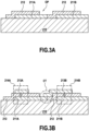
- Figure 3A is a cross section of a structure which will form subsequently and as formed on figure 3B an integrated component.
- This structure comprises a substrate 210 which can be a semiconductor substrate, or even an insulating substrate.
- a first bottom conductive region 211A and a second bottom conductive region 211B separated from the first bottom conductive region are formed by depositing a conductive layer and patterning this layer to obtain the two regions.
- a dielectric layer 212 is formed, here in a conformal manner.
- An opening OP is formed in this layer above the first bottom conductive region.
- a first top conductive region 213A is formed above the dielectric layer 212 and above the first bottom conductive region so as to form a first capacitor 214A.
- a second top conductive region 213B is formed above the dielectric layer 212 and above the second bottom conductive region so as to form second first capacitor 214B.
- the second top conductive region extends to the opening OP of the dielectric layer so as to form an electrical connection CT between the second top conductive region and the first bottom conductive region, and so as to connect the first capacitor and the second capacitor.
- This structure allows obtaining more flexibility on the type of substrate.
- additional electrodes can be formed, and the substrate can be connected to any one of the electrodes.
- Figure 4 is a top view of an electrical device 300 comprising a board BRD and a plurality of dividing stages each consisting in a distinct integrated component.
- three dividing stages/integrated components 200A, 200B, and 200C are assembled on the board, using a chip-on-board technique, and wire bonding.
- the integrated components 200A, 200B, and 200C are identical and have a structure which is similar to the component described in reference to figure 2 .
- the board BRD comprises an input terminal 301 for receiving an input voltage, and a wire WBI is bonded between this input terminal and the intermediary input terminal 204A of component 200A.
- Another wire WBAB is bonded between the intermediary output terminal 206A and the intermediary input terminal 204B to connect the dividing stages 200A and 200B.
- a wire WBBC is bonded between the intermediary output terminal 206B and the intermediary input terminal 204A.
- the intermediary output terminal 206C is connected to the output terminal 302 of the board.
- Wires are also used to connect the dividing stages to a ground terminal 303 arranged on the board.
- the above described voltage dividers use capacitors that have capacitance values that can be disregarded when designing a voltage divider as long as the dividing ratio is known.
- This dividing ratio is particularly stable, as all the capacitors of a stage are formed in a same integrated component (and will therefore be affected similarly by an elevation of temperature, for example - it should be noted that this is also an advantage over MLCC components where the temperature derating is component dependent).
- the present voltage divider benefits from the advantages of using a semiconductor substrate to manufacture capacitors.
- the capacitance used can be small, as only the ratio is relevant.
Landscapes
- Engineering & Computer Science (AREA)
- Physics & Mathematics (AREA)
- Electromagnetism (AREA)
- General Physics & Mathematics (AREA)
- Radar, Positioning & Navigation (AREA)
- Automation & Control Theory (AREA)
- Power Engineering (AREA)
- Microelectronics & Electronic Packaging (AREA)
- Semiconductor Integrated Circuits (AREA)
Abstract
wherein each dividing stage comprises a plurality of capacitors, and for each dividing stage, the plurality of capacitors of this dividing stage is arranged in a same integrated component (200A, 200B, 200C) assembled on the board and electrically connected between the input terminal and the output terminal.
Description
- The present invention relates to the field of electrical devices, and more precisely to the field of electrical devices including AC voltage dividers.
- AC voltage dividers are typically used in power applications where AC voltages need to be divided.
- To this end, discrete Multilayer Ceramic Capacitors (MLCC) are assembled using Chip-On-Board (COB) techniques as high capacitance values can be required. It can be conceived that the capacitance values of these MLCC capacitors need to be carefully monitored when used in a voltage divider. By way of example, a tolerance of 2% on the capacitance value, or even 1%, can be required. This can be particularly difficult to achieve, and requires a preliminary sorting of the components.
- The MLCC components can have a size of the order of 3.2mm by 1.6mm, which may be an issue in terms of integration and compactness. In particular, for high voltage applications where the MLCC components are located close to inverters, the available space is limited and the thermal constraints are critical.
- These systems are prone to risks of sparks/short-circuits, and also derating. MLCC components are particularly known for their derating (this is also true for other types of capacitors such as tantalum capacitors and electrochemical capacitors).
- From the prior art, the following documents are known:
- Document
CN 105137378 discloses a voltage divider which self-calibrates. - Document
US 10461040 - Document
CN 101915860 discloses a voltage divider terminal structure. - Document
US 6518814 discloses an integrated voltage capacitor formed above an SOI substrate. - There exists a need for precisely matched capacitors that can be used in voltage dividers.
- The present invention has been made in the light of the above problems.
- The present invention provides an electrical device comprising a board, an AC voltage divider comprising a plurality of dividing stages each associated with a dividing ratio, an input terminal arranged on the board for receiving an input voltage, and an output terminal arranged on the board for outputting a divided voltage,
- wherein each dividing stage comprises a plurality of capacitors, and for each dividing stage, the plurality of capacitors of this dividing stage is arranged in a same integrated component assembled on the board and electrically connected between the input terminal and the output terminal.
- A dividing stage comprises an intermediary input terminal (arranged on the integrated component), an intermediary output terminal (arranged on the integrated component, typically connected to the middle point between two capacitors), and a ground terminal (arranged on the integrated component). The intermediary input terminal can be connected to the input terminal of the board or to an intermediary output terminal of another dividing stage, and the intermediary output terminal can be connected to the output terminal of the board or to an intermediary input terminal of another dividing stage.
- By way of example, a stage comprises two capacitors.
- By forming the capacitors of a same stage in an integrated component, these capacitors can be formed using parallel manufacturing techniques, which reduces the possibility of a mismatch between the electrical parameters of these capacitors. In fact, a deviation of any electrical parameter (for example the capacitance which varies in accordance with a dielectric thickness deviating from a nominal value) can affect the individual electrical parameters of the capacitors but not the dividing ratio of the stage corresponding to this component, as long as deviations are proportional to the nominal values. Consequently, by grouping together capacitors of a same dividing stage in an integrated component, tolerance requirements on individual components are loosened as the dividing ratio is not always affected when a parameter deviates from its nominal value.
- Further, the capacitors of a same integrated component will be affected by temperature similarly, while the dividing ratio may remain stable.
- It has been observed that the individual capacitance values are not as useful as the dividing ratios, when designing a voltage divider. Hence, the proposed structure overcomes the need to control the individual capacitance values.
- Any integrated manufacturing technology can be used, as long as the same manufacturing process is used to manufacture all the capacitors of a same dividing stage, in parallel.
- This results in a matching between the capacitors of a same stage. By a matching, what is meant is that specific parameters of these capacitors will be identical, for example: the dielectric thickness, the dielectric composition, the electrode thickness, the electrode composition. In fact, this matching is a consequence of manufacturing the capacitors of a same stage in a same integrated component, which share the same manufacturing steps (they are preferably manufactured in parallel - as they are made in a same integrated component).
- Also, integrating capacitors in an integrated component increases the reliability of the device and prevents the occurrence of sparks in high voltage applications (while also allowing low voltage applications).
- According to a particular embodiment, the device comprises a plurality of distinct integrated components, each integrated component comprising the plurality of capacitors of a single dividing stage.
- It has been observed that it is preferable to separate the dividing stages into a plurality of distinct integrated components as these dividing stages operate at different voltages and this provides a good insulation between the stages.
- According to a particular embodiment, an integrated component comprises the plurality of capacitors of at least two dividing stages.
- Alternatively, it is possible to conceive an integrated component including several dividing stages.
- According to a particular embodiment, each dividing stage comprises only two capacitors (and no other passive component except connections and terminals).
- According to a particular embodiment, each integrated component comprises an intermediary output port connected to the two capacitors (typically a middle point).
- This intermediary output port allows exiting the integrated component so as to form a connection (for example using wire bonding) with a terminal on the board or with another integrated component (of another dividing stage).
- According to a particular embodiment, the capacitors are 3D capacitors.
- For example, a 3D capacitor comprises functional electrodes presenting a relief (for example they comprise a surface presenting a relief or they are formed on a relief such as a pore, a hole, a trench, or a pillar). 3D capacitors may also be defined as comprising functional electrodes extending in three directions orthogonal with each other (for example two directions parallel to the support and one direction orthogonal with the support). In the invention a functional electrode is an electrode which faces the other electrode of the capacitor and participates to the capacitance of the device. The capacitor terminals may be included in the functional electrodes, partially included in the functional electrodes, or may be connected to the functional electrodes. A functional electrode extending in the three directions is a functional electrode having an outer surface extending in these three directions.
- According to a particular embodiment, capacitors arranged in a same integrated component are supported by a same semiconductor substrate (typically a silicon substrate).
- By supported by, what is meant is that they are formed above or in this substrate, and for example arranged next to each other on this substrate.
- According to a particular embodiment, the same semiconductor substrate (supporting the two capacitors) comprises a semiconductor region forming an electrode of each of said capacitors supported by the semiconductor substrate.
- For example, the capacitors can be capacitors formed in accordance with the manufacturing processes described in document
WO 2007/125510 . - According to a particular embodiment, each integrated component is assembled as a chip-on-board module on the board.
- According to a particular embodiment, an integrated component (i.e. an integrated component including a dividing stage having at least two capacitors) comprises:
- a substrate (for example a semiconductor substrate),
- above the substrate, a first bottom conductive region and a second bottom conductive region separated from the first bottom conductive region (for example formed by depositing and patterning a conductive layer),
- a dielectric layer above the two separated conductive regions and the substrate, the dielectric layer having at least one opening above the first bottom conductive region (a through-opening that opens onto the first bottom conductive region),
- a first top conductive region arranged above the dielectric layer and the first bottom conductive region so as to form a first capacitor (formed by the first bottom conductive region, the dielectric layer, and the first top conductive region facing the bottom conductive region),
- a second top conductive region arranged above the dielectric layer and the second bottom conductive region so as to form a second capacitor (formed by the second bottom conductive region, the dielectric layer, and the second top conductive region facing the bottom conductive region),
- wherein the second top conductive region extends to the opening of the dielectric layer so as to form an electrical connection between the second top conductive region and the first bottom conductive region, and so as to connect the first capacitor and the second capacitor (the second top conductive region forms an intermediary output port).
- In this particular embodiment, the capacitor electrodes can be formed from a same layer, and the dielectric layer is shared between the two capacitors. A good matching is obtained.
- This structure is also advantageous for some applications as the substrate can remain insulating and may not have to be used to form a capacitor electrode (typically the shared electrode between the capacitors). This can be used in situations where the material of the substrate is difficult to transform into a conductive material.
- This structure also allows using a substrate which has to be connected to the ground. For example a supplementary insulating layer can be arranged between the substrate and the capacitors, eventually with an opening in this insulating layer to form an electrical connection between the substrate and a capacitor electrode which should be connected to the ground. Alternatively, the substrate may be locally doped to form a diode in a blocking state when the dividing stage is being used.
- Also, this structure is advantageous when multiple integrated components have to be arranged close to one another as a non-conductive substrate prevents any electrical breakdown.
- Finally, it should be noted that this structure is manufactured using steps analogous to the steps used to form MIMIM structures, well known to the person skilled in the art.
- The invention further provides a method of manufacturing an electrical device comprising an AC voltage divider, the method comprising:
- providing a board equipped with an input terminal for receiving an input voltage and an output terminal for outputting a divided voltage,
- forming a plurality of dividing stages each associated with a dividing ratio, wherein each dividing stage comprises a plurality of capacitors, and for each dividing stage, the plurality of capacitors of this dividing stage is arranged in a same integrated component, and
- assembling each integrated component on the board (or assembling the integrated component if all the dividing stages are arranged in a same integrated component), so as to electrically connect each integrated component between the input terminal and the output terminal.
- This method can be adapted to the manufacture of any one of the embodiments of the device as defined above.
- According to a particular embodiment, the method comprises using a chip-on-board process to assemble each integrated component on the board.
- According to a particular embodiment, for each integrated component, the method comprises forming the capacitors of this integrated component using at least one parallel manufacturing process.
- For example, the capacitors can be formed using a same deposition step, a same photolithography step, etc.
- According to a particular embodiment, forming the plurality of capacitors of a same dividing stage in an integrated component comprises:
- providing a substrate,
- forming, above the substrate, a first bottom conductive region and a second bottom conductive region (for example by depositing a conductive layer and subsequently patterning this layer),
- forming a dielectric layer above the two separated conductive regions and the substrate, the dielectric layer having at least one opening above the first bottom conductive region (for example by depositing a dielectric layer and subsequently patterning this layer to form the opening),
- forming a first top conductive region above the dielectric layer and the first bottom conductive region so as to form a first capacitor,
- forming a second top conductive region above the dielectric layer and the second bottom conductive region so as to form a second capacitor (for example by depositing a conductive layer and subsequently patterning this layer to obtain both the first and the second top conductive regions),
- wherein the second top conductive region extends to the opening of the dielectric layer so as to form an electrical connection between the second top conductive region and the first bottom conductive region, and so as to connect the first capacitor and the second capacitor.
- Further features and advantages of the present invention will become apparent from the following description of certain embodiments thereof, given by way of illustration only, not limitation, with reference to the accompanying drawings in which:
-
Figure 1 is a circuit diagram of an electrical device according to an example, -
Figure 2 is a cross section of an integrated component according to an example, -
Figures 3A and 3B illustrate forming an integrated component according to another example, -
Figure 4 is a top view of an electrical device according to an example. - We will now describe an electrical device comprising an AC voltage divider which uses integrated components equipped with dividing stages.
- This device can be adapted for high-voltage applications (as will be described hereinafter in reference to
figure 1 ), but also for low-voltage applications, as the capacitors are arranged in integrated devices and can benefit from the advantages of silicon technology, for example. -
Figure 1 is a circuit diagram of adevice 100 including a voltage divider. The board and the integrated components that form this voltage divider will be visible on the exemplary representations offigures 2 ,3A ,3B and4 . - The device of
figure 1 comprises aninput terminal 101 able to receive a voltage of 1500V (high-voltage application), and anoutput terminal 102 which, through the voltage divider's operation, is configured to output a voltage of 5V. - To achieve this, a first dividing stage is connected to the
input terminal 101. This first dividing stage comprises acapacitor 103A, connected to the input terminal and to an intermediary output terminal 104 (the output terminal of the first dividing stage), and acapacitor 103B, connected to theintermediary output terminal 104 and to the ground GND.Capacitor 103A has a capacitance of 1pF whilecapacitor 103B has a capacitance of 5.7pF. Bothcapacitors - A second dividing stage is connected to the
intermediary output terminal 104. This second dividing stage comprises acapacitor 105A, connected to theintermediary output terminal 104 and to an intermediary output terminal 106 (the output terminal of the second dividing stage), and acapacitor 105B, connected to theintermediary output terminal 106 and to the ground GND.Capacitor 105A has a capacitance of 1pF whilecapacitor 105B has a capacitance of 5.7pF. Bothcapacitors - A third dividing stage is connected to the
intermediary output terminal 106. This third dividing stage comprises acapacitor 107A, connected to theintermediary output terminal 106 and to theoutput terminal 102, and acapacitor 107B, connected to theoutput terminal 102 and to the ground GND.Capacitor 107A has a capacitance of 1pF whilecapacitor 107B has a capacitance of 5.7pF. Bothcapacitors - It should be noted that in the circuit of
figure 1 , a deviation of a parameter of which will affect the capacitance (with respect to a nominal capacitance value) of a capacitor of a dividing stage will also affect the capacitance (also with respect to a nominal capacitance value) of the other capacitor of this same stage, because there is a matching of their parameters as they have been manufactured in parallel. Hence, the dividing ratio may be unaffected by a deviation of both capacitances. -
Figure 2 is a cross section of anintegrated component 200 that comprises twocapacitors figure 1 . - Both
capacitors - The
semiconductor substrate 203 is used to connect the two electrodes of the capacitors. For example, it can be doped so as to be conductive in its entirety or locally doped so as to form an electrical connection between thecapacitors - The first capacitor will have its remaining elements, in addition to its bottom electrode formed in the
substrate 203, above the substrate. Here, a dielectric region DI1 is formed above the substrate and anupper electrode 204 is formed on the dielectric region DI1. Theupper electrode 204 is a connecting pad which allows a wire to be bonded. It also forms the intermediary input of the dividing stage. - The second also has its remaining elements, in addition to its bottom electrode formed in the
substrate 203, above the substrate. Here, a dielectric region DI2 is formed above the substrate and anupper electrode 205 is formed on the dielectric region DI1. Theupper electrode 204 is a connecting pad which allows a wire to be bonded, for example for a connection to the ground. - An
electrical contact 206 is formed on the substrate, in the form of a connecting pad. Thiselectrical contact 206 forms the intermediary output terminal of the dividing stage of this integrated component. - It should be noted that for the sake of simplicity, the capacitors are represented as 2D capacitors. However, in order to increase the capacitance of the capacitors, it is possible to use 3D capacitors. By way of example, 3D structures can be formed in the
semiconductor substrate 203 to form pillars, trenches, or holes, that are then filled with a stack of dielectric and electrode. -
Figure 3A is a cross section of a structure which will form subsequently and as formed onfigure 3B an integrated component. This structure comprises asubstrate 210 which can be a semiconductor substrate, or even an insulating substrate. - Above the
substrate 210, a first bottomconductive region 211A and a second bottomconductive region 211B separated from the first bottom conductive region are formed by depositing a conductive layer and patterning this layer to obtain the two regions. - Then, a
dielectric layer 212 is formed, here in a conformal manner. An opening OP is formed in this layer above the first bottom conductive region. - As shown on
figure 3B , a first topconductive region 213A is formed above thedielectric layer 212 and above the first bottom conductive region so as to form afirst capacitor 214A. - Also, a second top
conductive region 213B is formed above thedielectric layer 212 and above the second bottom conductive region so as to form secondfirst capacitor 214B. - The second top conductive region extends to the opening OP of the dielectric layer so as to form an electrical connection CT between the second top conductive region and the first bottom conductive region, and so as to connect the first capacitor and the second capacitor.
- This structure allows obtaining more flexibility on the type of substrate.
- Also, additional electrodes can be formed, and the substrate can be connected to any one of the electrodes.
-
Figure 4 is a top view of anelectrical device 300 comprising a board BRD and a plurality of dividing stages each consisting in a distinct integrated component. - More precisely, three dividing stages/
integrated components - The
integrated components figure 2 . - Here, the board BRD comprises an
input terminal 301 for receiving an input voltage, and a wire WBI is bonded between this input terminal and theintermediary input terminal 204A ofcomponent 200A. Another wire WBAB is bonded between theintermediary output terminal 206A and theintermediary input terminal 204B to connect the dividingstages stages intermediary output terminal 206B and theintermediary input terminal 204A. Finally, theintermediary output terminal 206C is connected to theoutput terminal 302 of the board. - Wires are also used to connect the dividing stages to a
ground terminal 303 arranged on the board. - In the illustrated example, if each dividing stage is associated with a dividing ratio Q=(X+Y)/X (where X is the capacitance of the capacitor connected to the input and Y the capacitance of the capacitor connected to the ground), the output voltage for a given input AC voltage U is U/Q3.
- The above described voltage dividers use capacitors that have capacitance values that can be disregarded when designing a voltage divider as long as the dividing ratio is known. This dividing ratio is particularly stable, as all the capacitors of a stage are formed in a same integrated component (and will therefore be affected similarly by an elevation of temperature, for example - it should be noted that this is also an advantage over MLCC components where the temperature derating is component dependent).
- The present voltage divider benefits from the advantages of using a semiconductor substrate to manufacture capacitors.
- Also, the capacitance used can be small, as only the ratio is relevant.
- Although the present invention has been described above with reference to certain specific embodiments, it will be understood that the invention is not limited by the particularities of the specific embodiments. Numerous variations, modifications and developments may be made in the above-described embodiments within the scope of the appended claims.
Claims (14)
- An electrical device comprising an AC voltage divider comprising a board (BRD), a plurality of dividing stages each associated with a dividing ratio (Q), an input terminal (301) arranged on the board for receiving an input voltage, and an output terminal (302) arranged on the board for outputting a divided voltage,
wherein each dividing stage comprises a plurality of capacitors, and for each dividing stage, the plurality of capacitors of this dividing stage is arranged in a same integrated component (200A, 200B, 200C) assembled on the board and electrically connected between the input terminal and the output terminal. - The device of claim 1, comprising a plurality of distinct integrated components (200A, 200B, 200C), each integrated component comprising the plurality of capacitors of a single dividing stage.
- The device of claim 1, wherein an integrated component comprises the plurality of capacitors of at least two dividing stages.
- The device of any one of claims 1 to 3, wherein each dividing stage comprises only two capacitors.
- The device of claims 3 and 4, wherein each integrated component comprises an intermediary output port (206A, 206B, 206C) connected to the two capacitors.
- The device of any one of claims 1 to 5, wherein the capacitors are 3D capacitors.
- The device of any one of claims 1 to 6, wherein capacitors arranged in a same integrated component are supported by a same semiconductor substrate (203).
- The device of claim 7, wherein the same semiconductor substrate comprises a semiconductor region forming an electrode of each of said capacitors supported by the semiconductor substrate.
- The device of any one of claim 1 to 8, wherein each integrated component is assembled as a chip-on-board module on the board.
- The device of any one of claims 1 to 9, wherein an integrated component comprises:a substrate (210),above the substrate, a first bottom conductive region (211A) and a second bottom conductive region (211B) separated from the first bottom conductive region,a dielectric layer (212) above the two separated conductive regions and the substrate, the dielectric layer having at least one opening (OP) above the first bottom conductive region,a first top conductive region (213A) arranged above the dielectric layer and the first bottom conductive region so as to form a first capacitor,a second top conductive region (213B) arranged above the dielectric layer and the second bottom conductive region so as to form a second capacitor,wherein the second top conductive region extends to the opening of the dielectric layer so as to form an electrical connection (CT) between the second top conductive region and the first bottom conductive region, and so as to connect the first capacitor and the second capacitor.
- A method of manufacturing an electrical device comprising an AC voltage divider, the method comprising:providing a board (BRD) equipped with an input terminal (301) for receiving an input voltage and an output terminal (302) for outputting a divided voltage,forming a plurality of dividing stages each associated with a dividing ratio, wherein each dividing stage comprises a plurality of capacitors, and for each dividing stage, the plurality of capacitors of this dividing stage is arranged in a same integrated component (200A, 200B, 200C), andassembling each integrated component on the board, so as to electrically connect each integrated component between the input terminal and the output terminal.
- The method of claim 11, comprising using a chip-on-board process to assemble each integrated component on the board.
- The method of claim 11 or 12, comprising, for each integrated component, forming the capacitors of this integrated component using at least one parallel manufacturing process.
- The method of any one of claims 11 to 13, wherein forming the plurality of capacitors of a same dividing stage in an integrated component comprises:providing a substrate (210),forming, above the substrate, a first bottom conductive region (211A) and a second bottom conductive region (211B),forming a dielectric layer (212) above the two separated conductive regions and the substrate, the dielectric layer having at least one opening (OP) above the first bottom conductive region,forming a first top conductive region (213A) above the dielectric layer and the first bottom conductive region so as to form a first capacitor,forming a second top conductive region (213B) above the dielectric layer and the second bottom conductive region so as to form a second capacitor,wherein the second top conductive region extends to the opening of the dielectric layer so as to form an electrical connection (CT) between the second top conductive region and the first bottom conductive region, and so as to connect the first capacitor and the second capacitor.
Priority Applications (3)
| Application Number | Priority Date | Filing Date | Title |
|---|---|---|---|
| EP21306167.4A EP4142133A1 (en) | 2021-08-30 | 2021-08-30 | An electrical device comprising an ac voltage divider and capacitors arranged in integrated components |
| US17/898,738 US20230060343A1 (en) | 2021-08-30 | 2022-08-30 | Electrical device comprising an ac voltage divider and capacitors arranged in integrated components |
| CN202211050922.4A CN115732232A (en) | 2021-08-30 | 2022-08-30 | Electrical installations comprising AC voltage dividers and capacitors arranged in integrated components |
Applications Claiming Priority (1)
| Application Number | Priority Date | Filing Date | Title |
|---|---|---|---|
| EP21306167.4A EP4142133A1 (en) | 2021-08-30 | 2021-08-30 | An electrical device comprising an ac voltage divider and capacitors arranged in integrated components |
Publications (1)
| Publication Number | Publication Date |
|---|---|
| EP4142133A1 true EP4142133A1 (en) | 2023-03-01 |
Family
ID=77838790
Family Applications (1)
| Application Number | Title | Priority Date | Filing Date |
|---|---|---|---|
| EP21306167.4A Pending EP4142133A1 (en) | 2021-08-30 | 2021-08-30 | An electrical device comprising an ac voltage divider and capacitors arranged in integrated components |
Country Status (3)
| Country | Link |
|---|---|
| US (1) | US20230060343A1 (en) |
| EP (1) | EP4142133A1 (en) |
| CN (1) | CN115732232A (en) |
Citations (17)
| Publication number | Priority date | Publication date | Assignee | Title |
|---|---|---|---|---|
| EP0520434A1 (en) * | 1991-06-26 | 1992-12-30 | Hughes Aircraft Company | Integrated socket-type package for flip chip semiconductor devices and circuits |
| US5471178A (en) * | 1994-02-03 | 1995-11-28 | Motorola, Inc. | Ladder filter and method for producing conjugately matched impedance |
| US5813881A (en) * | 1994-02-08 | 1998-09-29 | Prolinx Labs Corporation | Programmable cable and cable adapter using fuses and antifuses |
| US6518814B1 (en) | 1999-12-28 | 2003-02-11 | Koninklijke Philips Electronics N.V. | High-voltage capacitor voltage divider circuit having a high-voltage silicon-on-insulation (SOI) capacitor |
| US20060185429A1 (en) * | 2005-02-21 | 2006-08-24 | Finemems Inc. | An Intelligent Integrated Sensor Of Tire Pressure Monitoring System (TPMS) |
| WO2007125510A2 (en) | 2006-05-02 | 2007-11-08 | Nxp B.V. | Electric device comprising an improved electrode with a pillar having protrusions or scores for enhanced stability |
| US20100019825A1 (en) * | 2008-07-25 | 2010-01-28 | Texas Instruments Incorporated | Novel single supply level shifter circuit for multi-voltage designs, capable of up/down shifting |
| CN101915860A (en) | 2010-07-22 | 2010-12-15 | 无锡市锡容电力电器有限公司 | Integrated output terminal structure of capacitive voltage divider |
| US20120306676A1 (en) * | 2009-11-04 | 2012-12-06 | Harish Balasubramaniam | Capacitive voltage divider |
| CN105137378A (en) | 2015-08-14 | 2015-12-09 | 中国电力科学研究院 | 2/1 voltage ratio self-calibration method of voltage divider |
| CN109406851A (en) * | 2018-12-13 | 2019-03-01 | 西安交通大学 | A kind of coaxial type resistance divider and its high frequency response compensation method |
| US20190130957A1 (en) * | 2017-10-27 | 2019-05-02 | Ferroelectric Memory Gmbh | Memory cell and methods thereof |
| CN109725193A (en) * | 2019-02-25 | 2019-05-07 | 云南电网有限责任公司红河供电局 | It is a kind of for running the suspension type neutral point undervoltage detection means for doing anti-defect diagonsis |
| US10461040B2 (en) | 2017-06-28 | 2019-10-29 | Apple Inc. | Matched ceramic capacitor structures |
| US20200234922A1 (en) * | 2019-01-22 | 2020-07-23 | Applied Materials, Inc. | Apparatus and method of generating a pulsed waveform |
| US20210013798A1 (en) * | 2011-05-05 | 2021-01-14 | Psemi Corporation | Power converters with modular stages |
| US20210210386A1 (en) * | 2014-11-24 | 2021-07-08 | Fraunhofer-Gesellschaft Zur Foerderung Der Angewandten Forschung E.V. | Capacitor and method for producing the same |
Family Cites Families (19)
| Publication number | Priority date | Publication date | Assignee | Title |
|---|---|---|---|---|
| US4418314A (en) * | 1980-10-20 | 1983-11-29 | The United States Of America As Represented By The Secretary Of The Army | High impedance fast voltage probe |
| JP2821194B2 (en) * | 1989-09-25 | 1998-11-05 | オリンパス光学工業株式会社 | Charge transfer device and driving method thereof |
| US5166858A (en) * | 1991-10-30 | 1992-11-24 | Xilinx, Inc. | Capacitor formed in three conductive layers |
| EP0631144A1 (en) * | 1993-06-24 | 1994-12-28 | Koninklijke Philips Electronics N.V. | High voltage differential sensor having a capacitive attenuator |
| DE19923211C2 (en) * | 1998-07-23 | 2001-05-10 | Karlsruhe Forschzent | Capacitive voltage divider for measuring high voltage pulses with millisecond pulse duration |
| US7240254B2 (en) * | 2000-09-21 | 2007-07-03 | Inapac Technology, Inc | Multiple power levels for a chip within a multi-chip semiconductor package |
| US7061308B2 (en) * | 2003-10-01 | 2006-06-13 | International Business Machines Corporation | Voltage divider for integrated circuits |
| US7763923B2 (en) * | 2005-12-29 | 2010-07-27 | Taiwan Semiconductor Manufacturing Co., Ltd. | Metal-insulator-metal capacitor structure having low voltage dependence |
| FR2940457B1 (en) * | 2008-12-18 | 2011-02-18 | Schneider Electric Ind Sas | CAPACITIVE DIVIDER DEVICE, VOLTAGE SENSOR, TRIGGER MODULE, AND ELECTRICAL PROTECTION APPARATUS PROVIDED WITH SUCH A DEVICE |
| US8063649B2 (en) * | 2009-04-03 | 2011-11-22 | Ut-Battelle, Llc | Broadband high impedance pickoff circuit |
| GB2486694B (en) * | 2010-12-22 | 2015-09-23 | Gigle Networks Iberia S L | Amplification circuit with large dynamic range |
| EP2992338A4 (en) * | 2013-05-02 | 2017-05-10 | Awesense Wireless Inc. | A voltage sensing unit for sensing voltage of high-power lines using a single-contact point and method of use thereof |
| DE102015202597B4 (en) * | 2015-02-12 | 2017-09-21 | Hagenuk KMT Kabelmeßtechnik GmbH | Circuit arrangement for cable testing, cable testing, cable diagnosis and / or cable fault location and device with such a circuit arrangement |
| US9601545B1 (en) * | 2015-10-15 | 2017-03-21 | Taiwan Semiconductor Manufacturing Co., Ltd. | Series MIM structures compatible with RRAM process |
| EP3223024B1 (en) * | 2016-03-23 | 2018-11-14 | 3M Innovative Properties Company | Elastic sleeve for a power conductor |
| EP3639043A1 (en) * | 2017-06-13 | 2020-04-22 | 3M Innovative Properties Company | High-voltage impedance assembly |
| EP3499246B1 (en) * | 2017-12-18 | 2024-04-17 | 3M Innovative Properties Company | Voltage divider assembly |
| EP3578998B1 (en) * | 2018-06-08 | 2024-09-04 | 3M Innovative Properties Company | Impedance assembly |
| EP3840135B1 (en) * | 2019-12-20 | 2023-09-13 | 3M Innovative Properties Company | Retrofittable voltage sensing device for power networks |
-
2021
- 2021-08-30 EP EP21306167.4A patent/EP4142133A1/en active Pending
-
2022
- 2022-08-30 CN CN202211050922.4A patent/CN115732232A/en active Pending
- 2022-08-30 US US17/898,738 patent/US20230060343A1/en not_active Abandoned
Patent Citations (17)
| Publication number | Priority date | Publication date | Assignee | Title |
|---|---|---|---|---|
| EP0520434A1 (en) * | 1991-06-26 | 1992-12-30 | Hughes Aircraft Company | Integrated socket-type package for flip chip semiconductor devices and circuits |
| US5471178A (en) * | 1994-02-03 | 1995-11-28 | Motorola, Inc. | Ladder filter and method for producing conjugately matched impedance |
| US5813881A (en) * | 1994-02-08 | 1998-09-29 | Prolinx Labs Corporation | Programmable cable and cable adapter using fuses and antifuses |
| US6518814B1 (en) | 1999-12-28 | 2003-02-11 | Koninklijke Philips Electronics N.V. | High-voltage capacitor voltage divider circuit having a high-voltage silicon-on-insulation (SOI) capacitor |
| US20060185429A1 (en) * | 2005-02-21 | 2006-08-24 | Finemems Inc. | An Intelligent Integrated Sensor Of Tire Pressure Monitoring System (TPMS) |
| WO2007125510A2 (en) | 2006-05-02 | 2007-11-08 | Nxp B.V. | Electric device comprising an improved electrode with a pillar having protrusions or scores for enhanced stability |
| US20100019825A1 (en) * | 2008-07-25 | 2010-01-28 | Texas Instruments Incorporated | Novel single supply level shifter circuit for multi-voltage designs, capable of up/down shifting |
| US20120306676A1 (en) * | 2009-11-04 | 2012-12-06 | Harish Balasubramaniam | Capacitive voltage divider |
| CN101915860A (en) | 2010-07-22 | 2010-12-15 | 无锡市锡容电力电器有限公司 | Integrated output terminal structure of capacitive voltage divider |
| US20210013798A1 (en) * | 2011-05-05 | 2021-01-14 | Psemi Corporation | Power converters with modular stages |
| US20210210386A1 (en) * | 2014-11-24 | 2021-07-08 | Fraunhofer-Gesellschaft Zur Foerderung Der Angewandten Forschung E.V. | Capacitor and method for producing the same |
| CN105137378A (en) | 2015-08-14 | 2015-12-09 | 中国电力科学研究院 | 2/1 voltage ratio self-calibration method of voltage divider |
| US10461040B2 (en) | 2017-06-28 | 2019-10-29 | Apple Inc. | Matched ceramic capacitor structures |
| US20190130957A1 (en) * | 2017-10-27 | 2019-05-02 | Ferroelectric Memory Gmbh | Memory cell and methods thereof |
| CN109406851A (en) * | 2018-12-13 | 2019-03-01 | 西安交通大学 | A kind of coaxial type resistance divider and its high frequency response compensation method |
| US20200234922A1 (en) * | 2019-01-22 | 2020-07-23 | Applied Materials, Inc. | Apparatus and method of generating a pulsed waveform |
| CN109725193A (en) * | 2019-02-25 | 2019-05-07 | 云南电网有限责任公司红河供电局 | It is a kind of for running the suspension type neutral point undervoltage detection means for doing anti-defect diagonsis |
Also Published As
| Publication number | Publication date |
|---|---|
| CN115732232A (en) | 2023-03-03 |
| US20230060343A1 (en) | 2023-03-02 |
Similar Documents
| Publication | Publication Date | Title |
|---|---|---|
| US7411776B2 (en) | Multilayer capacitor array | |
| US10468187B2 (en) | Thin-film ceramic capacitor having capacitance forming portions separated by separation slit | |
| US11038012B2 (en) | Capacitor device and manufacturing method therefor | |
| US11158553B2 (en) | Package and semiconductor device | |
| US9117589B2 (en) | Capacitor structure and stack-type capacitor structure | |
| TWI754973B (en) | A capacitor structure | |
| CN101345133B (en) | Multilayer capacitor | |
| KR20040067784A (en) | Semiconductor device | |
| CN116207082B (en) | Capacitor, manufacturing method and working method thereof | |
| US12317521B2 (en) | Capacitor device and manufacturing method therefor | |
| KR101020530B1 (en) | Multilayer Capacitor Array | |
| US10720280B2 (en) | Thin-film ceramic capacitor having capacitance forming portions separated by separation slit | |
| KR20230002353A (en) | Metal-Insulator-Metal (MIM) Energy Storage Device and Manufacturing Method with a Stacked Stack | |
| JP2001210544A (en) | Chip multilayer ceramic capacitor | |
| US11756989B2 (en) | Capacitor integrated structure | |
| US20230060343A1 (en) | Electrical device comprising an ac voltage divider and capacitors arranged in integrated components | |
| JP2015041735A (en) | Capacitor element | |
| KR20170028700A (en) | Multilayer electronic component, board having the same | |
| US7948737B2 (en) | Multilayer capacitor array | |
| US10199166B2 (en) | Capacitor | |
| CN111357103A (en) | Capacitor with a capacitor element | |
| CN104851590A (en) | Capacitor with multiple types of capacitance | |
| CN112652619B (en) | Gasket and manufacturing method thereof, and packaging structure and manufacturing method thereof | |
| JP4952779B2 (en) | Multilayer capacitor array | |
| KR20160058509A (en) | Multi-layer ceramic capacitor |
Legal Events
| Date | Code | Title | Description |
|---|---|---|---|
| PUAI | Public reference made under article 153(3) epc to a published international application that has entered the european phase |
Free format text: ORIGINAL CODE: 0009012 |
|
| STAA | Information on the status of an ep patent application or granted ep patent |
Free format text: STATUS: THE APPLICATION HAS BEEN PUBLISHED |
|
| AK | Designated contracting states |
Kind code of ref document: A1 Designated state(s): AL AT BE BG CH CY CZ DE DK EE ES FI FR GB GR HR HU IE IS IT LI LT LU LV MC MK MT NL NO PL PT RO RS SE SI SK SM TR |
|
| STAA | Information on the status of an ep patent application or granted ep patent |
Free format text: STATUS: REQUEST FOR EXAMINATION WAS MADE |
|
| 17P | Request for examination filed |
Effective date: 20230821 |
|
| RBV | Designated contracting states (corrected) |
Designated state(s): AL AT BE BG CH CY CZ DE DK EE ES FI FR GB GR HR HU IE IS IT LI LT LU LV MC MK MT NL NO PL PT RO RS SE SI SK SM TR |
|
| STAA | Information on the status of an ep patent application or granted ep patent |
Free format text: STATUS: EXAMINATION IS IN PROGRESS |
|
| 17Q | First examination report despatched |
Effective date: 20241025 |