EP4142131B1 - Multi-level direct current converter and power supply system - Google Patents
Multi-level direct current converter and power supply system Download PDFInfo
- Publication number
- EP4142131B1 EP4142131B1 EP22192344.4A EP22192344A EP4142131B1 EP 4142131 B1 EP4142131 B1 EP 4142131B1 EP 22192344 A EP22192344 A EP 22192344A EP 4142131 B1 EP4142131 B1 EP 4142131B1
- Authority
- EP
- European Patent Office
- Prior art keywords
- direct current
- voltage
- power transistor
- current converter
- power
- Prior art date
- Legal status (The legal status is an assumption and is not a legal conclusion. Google has not performed a legal analysis and makes no representation as to the accuracy of the status listed.)
- Active
Links
- 239000003990 capacitor Substances 0.000 claims description 53
- 238000006243 chemical reaction Methods 0.000 claims description 14
- 230000005669 field effect Effects 0.000 claims description 7
- 239000004065 semiconductor Substances 0.000 claims description 7
- 238000000034 method Methods 0.000 description 21
- 238000010586 diagram Methods 0.000 description 15
- 238000004146 energy storage Methods 0.000 description 4
- 238000001914 filtration Methods 0.000 description 3
- 238000004904 shortening Methods 0.000 description 3
- 208000025274 Lightning injury Diseases 0.000 description 2
- 238000005516 engineering process Methods 0.000 description 2
- 230000003287 optical effect Effects 0.000 description 2
- 230000009286 beneficial effect Effects 0.000 description 1
- 230000008878 coupling Effects 0.000 description 1
- 238000010168 coupling process Methods 0.000 description 1
- 238000005859 coupling reaction Methods 0.000 description 1
- 238000001514 detection method Methods 0.000 description 1
Images


Classifications
-
- H—ELECTRICITY
- H02—GENERATION; CONVERSION OR DISTRIBUTION OF ELECTRIC POWER
- H02M—APPARATUS FOR CONVERSION BETWEEN AC AND AC, BETWEEN AC AND DC, OR BETWEEN DC AND DC, AND FOR USE WITH MAINS OR SIMILAR POWER SUPPLY SYSTEMS; CONVERSION OF DC OR AC INPUT POWER INTO SURGE OUTPUT POWER; CONTROL OR REGULATION THEREOF
- H02M7/00—Conversion of ac power input into dc power output; Conversion of dc power input into ac power output
- H02M7/42—Conversion of dc power input into ac power output without possibility of reversal
- H02M7/44—Conversion of dc power input into ac power output without possibility of reversal by static converters
- H02M7/48—Conversion of dc power input into ac power output without possibility of reversal by static converters using discharge tubes with control electrode or semiconductor devices with control electrode
- H02M7/483—Converters with outputs that each can have more than two voltages levels
- H02M7/4837—Flying capacitor converters
-
- H—ELECTRICITY
- H02—GENERATION; CONVERSION OR DISTRIBUTION OF ELECTRIC POWER
- H02M—APPARATUS FOR CONVERSION BETWEEN AC AND AC, BETWEEN AC AND DC, OR BETWEEN DC AND DC, AND FOR USE WITH MAINS OR SIMILAR POWER SUPPLY SYSTEMS; CONVERSION OF DC OR AC INPUT POWER INTO SURGE OUTPUT POWER; CONTROL OR REGULATION THEREOF
- H02M3/00—Conversion of dc power input into dc power output
- H02M3/02—Conversion of dc power input into dc power output without intermediate conversion into ac
- H02M3/04—Conversion of dc power input into dc power output without intermediate conversion into ac by static converters
- H02M3/06—Conversion of dc power input into dc power output without intermediate conversion into ac by static converters using resistors or capacitors, e.g. potential divider
- H02M3/07—Conversion of dc power input into dc power output without intermediate conversion into ac by static converters using resistors or capacitors, e.g. potential divider using capacitors charged and discharged alternately by semiconductor devices with control electrode, e.g. charge pumps
-
- H—ELECTRICITY
- H02—GENERATION; CONVERSION OR DISTRIBUTION OF ELECTRIC POWER
- H02H—EMERGENCY PROTECTIVE CIRCUIT ARRANGEMENTS
- H02H7/00—Emergency protective circuit arrangements specially adapted for specific types of electric machines or apparatus or for sectionalised protection of cable or line systems, and effecting automatic switching in the event of an undesired change from normal working conditions
- H02H7/10—Emergency protective circuit arrangements specially adapted for specific types of electric machines or apparatus or for sectionalised protection of cable or line systems, and effecting automatic switching in the event of an undesired change from normal working conditions for converters; for rectifiers
- H02H7/12—Emergency protective circuit arrangements specially adapted for specific types of electric machines or apparatus or for sectionalised protection of cable or line systems, and effecting automatic switching in the event of an undesired change from normal working conditions for converters; for rectifiers for static converters or rectifiers
- H02H7/1213—Emergency protective circuit arrangements specially adapted for specific types of electric machines or apparatus or for sectionalised protection of cable or line systems, and effecting automatic switching in the event of an undesired change from normal working conditions for converters; for rectifiers for static converters or rectifiers for DC-DC converters
-
- H—ELECTRICITY
- H02—GENERATION; CONVERSION OR DISTRIBUTION OF ELECTRIC POWER
- H02M—APPARATUS FOR CONVERSION BETWEEN AC AND AC, BETWEEN AC AND DC, OR BETWEEN DC AND DC, AND FOR USE WITH MAINS OR SIMILAR POWER SUPPLY SYSTEMS; CONVERSION OF DC OR AC INPUT POWER INTO SURGE OUTPUT POWER; CONTROL OR REGULATION THEREOF
- H02M1/00—Details of apparatus for conversion
- H02M1/0095—Hybrid converter topologies, e.g. NPC mixed with flying capacitor, thyristor converter mixed with MMC or charge pump mixed with buck
-
- H—ELECTRICITY
- H02—GENERATION; CONVERSION OR DISTRIBUTION OF ELECTRIC POWER
- H02M—APPARATUS FOR CONVERSION BETWEEN AC AND AC, BETWEEN AC AND DC, OR BETWEEN DC AND DC, AND FOR USE WITH MAINS OR SIMILAR POWER SUPPLY SYSTEMS; CONVERSION OF DC OR AC INPUT POWER INTO SURGE OUTPUT POWER; CONTROL OR REGULATION THEREOF
- H02M1/00—Details of apparatus for conversion
- H02M1/14—Arrangements for reducing ripples from dc input or output
-
- H—ELECTRICITY
- H02—GENERATION; CONVERSION OR DISTRIBUTION OF ELECTRIC POWER
- H02M—APPARATUS FOR CONVERSION BETWEEN AC AND AC, BETWEEN AC AND DC, OR BETWEEN DC AND DC, AND FOR USE WITH MAINS OR SIMILAR POWER SUPPLY SYSTEMS; CONVERSION OF DC OR AC INPUT POWER INTO SURGE OUTPUT POWER; CONTROL OR REGULATION THEREOF
- H02M1/00—Details of apparatus for conversion
- H02M1/36—Means for starting or stopping converters
-
- H—ELECTRICITY
- H02—GENERATION; CONVERSION OR DISTRIBUTION OF ELECTRIC POWER
- H02M—APPARATUS FOR CONVERSION BETWEEN AC AND AC, BETWEEN AC AND DC, OR BETWEEN DC AND DC, AND FOR USE WITH MAINS OR SIMILAR POWER SUPPLY SYSTEMS; CONVERSION OF DC OR AC INPUT POWER INTO SURGE OUTPUT POWER; CONTROL OR REGULATION THEREOF
- H02M3/00—Conversion of dc power input into dc power output
- H02M3/02—Conversion of dc power input into dc power output without intermediate conversion into ac
- H02M3/04—Conversion of dc power input into dc power output without intermediate conversion into ac by static converters
- H02M3/06—Conversion of dc power input into dc power output without intermediate conversion into ac by static converters using resistors or capacitors, e.g. potential divider
- H02M3/07—Conversion of dc power input into dc power output without intermediate conversion into ac by static converters using resistors or capacitors, e.g. potential divider using capacitors charged and discharged alternately by semiconductor devices with control electrode, e.g. charge pumps
- H02M3/072—Conversion of dc power input into dc power output without intermediate conversion into ac by static converters using resistors or capacitors, e.g. potential divider using capacitors charged and discharged alternately by semiconductor devices with control electrode, e.g. charge pumps adapted to generate an output voltage whose value is lower than the input voltage
-
- H—ELECTRICITY
- H02—GENERATION; CONVERSION OR DISTRIBUTION OF ELECTRIC POWER
- H02M—APPARATUS FOR CONVERSION BETWEEN AC AND AC, BETWEEN AC AND DC, OR BETWEEN DC AND DC, AND FOR USE WITH MAINS OR SIMILAR POWER SUPPLY SYSTEMS; CONVERSION OF DC OR AC INPUT POWER INTO SURGE OUTPUT POWER; CONTROL OR REGULATION THEREOF
- H02M3/00—Conversion of dc power input into dc power output
- H02M3/02—Conversion of dc power input into dc power output without intermediate conversion into ac
- H02M3/04—Conversion of dc power input into dc power output without intermediate conversion into ac by static converters
- H02M3/10—Conversion of dc power input into dc power output without intermediate conversion into ac by static converters using discharge tubes with control electrode or semiconductor devices with control electrode
- H02M3/145—Conversion of dc power input into dc power output without intermediate conversion into ac by static converters using discharge tubes with control electrode or semiconductor devices with control electrode using devices of a triode or transistor type requiring continuous application of a control signal
- H02M3/155—Conversion of dc power input into dc power output without intermediate conversion into ac by static converters using discharge tubes with control electrode or semiconductor devices with control electrode using devices of a triode or transistor type requiring continuous application of a control signal using semiconductor devices only
- H02M3/156—Conversion of dc power input into dc power output without intermediate conversion into ac by static converters using discharge tubes with control electrode or semiconductor devices with control electrode using devices of a triode or transistor type requiring continuous application of a control signal using semiconductor devices only with automatic control of output voltage or current, e.g. switching regulators
- H02M3/158—Conversion of dc power input into dc power output without intermediate conversion into ac by static converters using discharge tubes with control electrode or semiconductor devices with control electrode using devices of a triode or transistor type requiring continuous application of a control signal using semiconductor devices only with automatic control of output voltage or current, e.g. switching regulators including plural semiconductor devices as final control devices for a single load
-
- H—ELECTRICITY
- H02—GENERATION; CONVERSION OR DISTRIBUTION OF ELECTRIC POWER
- H02M—APPARATUS FOR CONVERSION BETWEEN AC AND AC, BETWEEN AC AND DC, OR BETWEEN DC AND DC, AND FOR USE WITH MAINS OR SIMILAR POWER SUPPLY SYSTEMS; CONVERSION OF DC OR AC INPUT POWER INTO SURGE OUTPUT POWER; CONTROL OR REGULATION THEREOF
- H02M7/00—Conversion of ac power input into dc power output; Conversion of dc power input into ac power output
- H02M7/42—Conversion of dc power input into ac power output without possibility of reversal
- H02M7/44—Conversion of dc power input into ac power output without possibility of reversal by static converters
- H02M7/48—Conversion of dc power input into ac power output without possibility of reversal by static converters using discharge tubes with control electrode or semiconductor devices with control electrode
- H02M7/483—Converters with outputs that each can have more than two voltages levels
- H02M7/487—Neutral point clamped inverters
-
- Y—GENERAL TAGGING OF NEW TECHNOLOGICAL DEVELOPMENTS; GENERAL TAGGING OF CROSS-SECTIONAL TECHNOLOGIES SPANNING OVER SEVERAL SECTIONS OF THE IPC; TECHNICAL SUBJECTS COVERED BY FORMER USPC CROSS-REFERENCE ART COLLECTIONS [XRACs] AND DIGESTS
- Y02—TECHNOLOGIES OR APPLICATIONS FOR MITIGATION OR ADAPTATION AGAINST CLIMATE CHANGE
- Y02E—REDUCTION OF GREENHOUSE GAS [GHG] EMISSIONS, RELATED TO ENERGY GENERATION, TRANSMISSION OR DISTRIBUTION
- Y02E10/00—Energy generation through renewable energy sources
- Y02E10/50—Photovoltaic [PV] energy
- Y02E10/56—Power conversion systems, e.g. maximum power point trackers
Definitions
- This application relates to the field of electronic circuit technologies, and in particular, to a multi-level direct current converter and a power supply system.
- direct current/direct current converters may be classified into two types: a two-level topology and a multi-level topology.
- Levels of a switching node of the two-level topology are 0 and an input voltage, and a switching node of the multilevel topology has more than two levels.
- a flying-capacitor clamped three-level direct current converter (three-level direct current converter for short) is one of DC/DC converters of the multi-level topology, and has the following feature: A half input voltage is stored by using a flying capacitor, so that a voltage of a switching node has three level states: 0, 1/2 of an input voltage, and the input voltage. Change amplitude of each time of switching of the three-level direct current converter changes to 1/2 of the input voltage, so that system performance can be improved by using a component with a low withstanding voltage and high performance.
- a voltage of the flying capacitor needs to reach 1/2 of the input voltage through precharging, to ensure normal operating of the three-level direct current converter.
- a charging loop of a flying capacitor Cf is mainly formed by using current sources I_in and I_out.
- a specific implementation is as follows: When an upper plate of Cf is charged by using I_in, a lower plate of Cf is discharged by an equal amount by using I_out.
- a voltage of the lower plate of Cf is controlled by using a feedback circuit, to ensure that there is enough voltage headroom between I_in and I_out, thereby charging Cf.
- the additional current sources and feedback circuit are required in the foregoing manner.
- a detection circuit is further required for stopping charging of Cf after detecting that precharging of Cf is completed.
- US-B-8503203 describes an apparatus for voltage conversion that includes a switched capacitor circuit, a pre-charge circuit, a voltage divider stage, and a driver stage.
- the switched capacitor circuit has pump capacitors to transfer energy and a steady-state operating mode and a pre-charge mode.
- the pre-charge circuit initially charges the pump capacitors when the switched capacitor circuit operates in the pre-charge mode.
- It includes a voltage divider stage having one or more nodes, each of which provides voltage at one of a corresponding one or more voltage levels, and a driver stage having one or more cascaded drivers, each of which comprises a first terminal for receiving a drive signal that depends at least in part on a voltage level at a corresponding one of the nodes, and a second terminal for coupling to a pump capacitor and to another of the drivers.
- a charging loop of a flying capacitor may be formed by configuring existing power transistors in the multi-level direct current converter, to precharge the flying capacitor, without an additional charging component, so that a structure is simple, and circuit costs are low.
- this application provides a multi-level direct current converter as defined in claim 1. No additional charging component is required in an entire charging process of the flying capacitor, so that a structure is simple, circuit costs are low, and applicability is strong.
- the voltage management unit is a voltage follower
- an input voltage of a non-inverting input end of the voltage follower is determined by the input voltage of the voltage input end
- an inverting input end of the voltage follower is connected to the second end of the first power transistor
- an output end of the voltage follower is used as the output end of the voltage management unit. Because the voltage follower has a simple structure, an area is reduced, and applicability is strong.
- the input voltage of the non-inverting input end of the voltage follower is ( N - 2)/( N - 1) of the input voltage of the voltage input end, where N is an integer greater than 2. Due to a concept of a virtual short circuit, the input voltage of the non-inverting input end and an input voltage of the inverting input end of the voltage follower are equal and are both ( N - 2)/( N - 1) of the input voltage, and the inverting input end is connected to a source of the first power transistor.
- a voltage of the source of the first power transistor is ( N - 2)/( N - 1) of the input voltage in the entire charging process of the flying capacitor.
- voltage stress of the first power transistor in the entire charging process of the flying capacitor is 1/( N - 1) of the input voltage. Therefore, in this manner, voltage stress of the first power transistor in the entire charging process can be effectively reduced, thereby prolonging a service life of the first power transistor.
- the voltage management unit includes a first resistor, a second resistor, a direct current source, and a third power transistor.
- One end of the first resistor is connected to the voltage input end and one end of the direct current source, the other end of the first resistor is connected to one end of the second resistor and a first end of the third power transistor, the other end of the second resistor is connected to the reference ground, the other end of the direct current source is connected to a second end of the third power transistor, a third end of the third power transistor is connected to the reference ground,
- the multi-level direct current converter is an N-level direct current converter, and a ratio between a resistance value of the first resistor and a resistance value of the second resistor is 1/( N - 2).
- the voltage management unit is implemented in various manners and has high flexibility.
- the third power transistor is a metal-oxide-semiconductor field-effect transistor MOSFET, and the first end, the second end, and the third end of the third power transistor are respectively a gate, a source, and a drain of the third power transistor. Due to a strong through-current capability of the MOSFET, a charging current may be appropriately increased within a tolerable current range of the power transistor in a charging process of the flying capacitor, thereby shortening precharging duration of the flying capacitor.
- the controller may further control the switching unit to disconnect the voltage management unit from the first power transistor and connect the controller to the third end of the first power transistor; and control the second power transistor to be cut off. Therefore, when the input voltage of the voltage input end rises to the target voltage, charging of the flying capacitor automatically ends, without an overcharge risk, so that precharging duration of the flying capacitor can be shortened by using a relatively large charging current.
- the direct current conversion unit further includes a fourth power transistor, and the fourth power transistor is connected to the second power transistor in parallel and is connected to the controller.
- the controller may further control the fourth power transistor to be conducted, until the input voltage of the voltage input end is the target voltage.
- a parallel charging branch circuit may be added by adding a parallel power transistor, to increase a charging current,. In this way, precharging duration of the flying capacitor is shortened, so that applicability is strong.
- the at least two power transistors further include a fifth power transistor and a sixth power transistor.
- the second end of the first power transistor is connected to a first end of the fifth power transistor
- a second end of the fifth power transistor is connected to a first end of the sixth power transistor
- a second end of the sixth power transistor is connected to the first end of the second power transistor
- a third end of the fifth power transistor and a third end of the sixth power transistor are both connected to the controller.
- each of the at least two power transistors connected to each other in series is a metal-oxide-semiconductor field-effect transistor MOSFET.
- a first end of each power transistor is a drain of the power transistor, a second end of the power transistor is a source of the power transistor, and a third end of the power transistor is a gate of the power transistor. Due to a strong through-current capability of the MOSFET, a charging current may be appropriately increased within a tolerable current range of the power transistor in a charging process of the flying capacitor, thereby shortening precharging duration of the flying capacitor.
- this application provides a power supply system.
- the power supply system includes a photovoltaic string and the multi-level direct current converter that is provided in any one of the first aspect to the possible implementations of the first aspect and that is connected to the photovoltaic string.
- the multi-level direct current converter is applicable to a photovoltaic power supply scenario, and has strong applicability.
- the power supply system further includes a direct current circuit breaker, and the photovoltaic string is connected to an input end of the multi-level direct current converter by using the direct current circuit breaker.
- the direct current circuit breaker can trigger overcurrent protection when an absolute value of a current exceeds a specific range of a rated current value, to cut off a current in a loop, thereby protecting the power supply system.
- the power supply system further includes a direct current combiner box, and the photovoltaic string is connected to an input end of the multilevel direct current converter by using the direct current combiner box. Because each input of the direct current combiner box is independently equipped with a solar photovoltaic direct-current high-voltage lightning protection circuit, the direct current combiner box has a multi-level lightning protection function, to ensure that a lightning stroke does not affect normal output of a photovoltaic array, thereby improving stability of the power supply system.
- the power supply system further includes an inverter, and an output end of the multi-level direct current converter is connected to the inverter.
- the power supply system further includes a direct current bus, and the output end of the multi-level direct current converter is connected to the inverter by using the direct current bus.
- a DC/DC converter is a commonly-used switching power supply component in an electronic system.
- a main function of the DC/DC converter is converting a direct current input voltage into a direct current output voltage of another electric potential, to meet a power supply requirement of an electronic system at a load end.
- DC/DC converters may be classified into two types: a two-level topology and a multilevel topology. Levels of a switching node of the two-level topology are 0 and an input voltage, and a switching node of the multi-level topology has more than two levels.
- a voltage of at least one flying capacitor in the multi-level direct current converter needs to reach a preset multiple of an input voltage through precharging, to ensure normal operating of the multi-level direct current converter, and keep stress at two ends of the power transistor within an allowable range.
- voltages of flying capacitors can be controlled by finely adjusting duty cycles.
- the flying capacitor needs to be precharged by using different voltage precharging circuits.
- a charging loop of a flying capacitor may be formed by configuring power transistors in the multi-level direct current converter, without an additional charging component, so that a structure is simple, and circuit costs are low.
- the multi-level direct current converter provided in this application may be adapted to different application scenarios, for example, a data center power supply scenario (to supply power to a load chip), a photovoltaic power supply scenario, an optical storage hybrid power supply scenario, and an energy storage power supply scenario.
- a photovoltaic power supply scenario a photovoltaic string is coupled to an input end of a multi-level direct current converter.
- the optical storage hybrid power supply scenario a photovoltaic string and an energy storage battery string are coupled to an input end of a multi-level direct current converter.
- an energy storage battery string is coupled to an input end of a multi-level direct current converter.
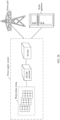
- FIG. 2a is a schematic diagram of an application scenario of a power supply system according to this application.
- the power supply system may include a power grid, an inverter, a primary DC/DC converter, and a secondary DC/DC converter.
- the power grid outputs an alternating current to an input end of the inverter.
- the inverter obtains a direct current voltage of 48 V after inverting the alternating current output by the power grid, and outputs the direct current voltage of 48 V to an input end of the primary DC/DC converter.
- the primary DC/DC converter obtains a direct current voltage of 12 V after performing step-down conversion on the direct current voltage of 48 V of the input end, and outputs the direct current voltage of 12 V to an input end of the secondary DC/DC converter.
- the secondary DC/DC converter obtains a direct current voltage of 1 V after performing step-down conversion on the direct current voltage of 12 V of the input end, and outputs the direct current voltage of 1 V to a load chip, to supply power to the load chip.
- the primary DC/DC converter or the secondary DC/DC converter herein is a multi-level direct current converter in this application. Because the multi-level direct current converter has a simple structure and low circuit costs, stability of the power supply system can be improved, and costs of the power supply system can be reduced, so that applicability is strong.
- FIG. 2b is a schematic diagram of another application scenario of a power supply system according to this application.
- the power supply system may include a photovoltaic string, a DC/DC converter, and an inverter.
- Each photovoltaic string may include a plurality of photovoltaic components connected in series and/or connected in parallel.
- An input end of the DC/DC converter is connected to the photovoltaic string, and is configured to: convert, through direct current conversion, a direct current voltage generated by the photovoltaic string connected to the input end into a direct current whose voltage is a preset value, and output the direct current to the inverter.
- An input end of the inverter is connected to an output end of the DC/DC converter, and is configured to invert the direct current output by the DC/DC converter into an alternating current, to supply power to various types of electrical equipment such as an alternating current power grid or an alternating current load (such as a home appliance).
- the power supply system may further include a direct current combiner box (not shown in the figure).
- the direct current combiner box may be disposed between a plurality of photovoltaic strings and the input end of the DC/DC converter, and is configured to combine input electric energy of the plurality of photovoltaic strings and then output combined electric energy. Because each input of the direct current combiner box is independently equipped with a solar photovoltaic direct-current high-voltage lightning protection circuit, the direct current combiner box has a multi-level lightning protection function, to ensure that a lightning stroke does not affect normal output of a photovoltaic array, thereby improving stability of the power supply system.
- the power supply system may further include a direct current circuit breaker (not shown in the figure).
- the direct current circuit breaker may be disposed between the photovoltaic string and the input end of the DC/DC converter, and is configured to trigger overcurrent protection when an absolute value of a current exceeds a specific range of a rated current value, to cut off a current in a loop, thereby protecting the power supply system.
- the power supply system may further include a direct current bus, and output ends of the DC/DC converters are connected to the input end of the inverter after being connected to the direct current bus in parallel.
- the DC/DC converter herein is a multi-level direct current converter in this application. Because the multi-level direct current converter has a simple structure and low circuit costs, stability of the power supply system can be improved, and costs of the power supply system can be reduced, so that applicability is strong.
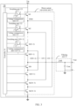
- FIG. 3 is a schematic diagram of a structure of a multi-level direct current converter according to this application.
- the multi-level direct current converter (an N-level direct current converter, where N is an integer greater than 2) includes a controller 10, a voltage management unit 111, a switching unit 121, and a direct current conversion unit 13.
- the direct current conversion unit 13 includes a flying capacitor Cf1 and at least two power transistors connected in series.
- the power transistors may be metal-oxide-semiconductor field-effect transistors MOSFETs.
- the at least two power transistors connected in series include a first power transistor M1 and a second power transistor M(2N-2).
- a drain of M1 is connected to a voltage input end Vin of the N-level direct current converter, a source of M1 is connected to a drain of M(2N-2) by using Cf1, and a source of M(2N-2) is connected to a reference ground.
- the at least two power transistors connected in series further include power transistors M2, ..., M(N-2), M(N-1), MN, M(N+1), ..., and M(2N-3).
- a drain of M2 is connected to the source of M1, ..., a source of M(N-2) is connected to a drain of M(N-1), a source of M(N-1) is connected to a drain of MN, a source of MN is connected to a drain of M(N+1), ..., and a source of M(2N-3) is connected to the drain of M(2N-2).
- the N-level direct current converter further includes flying capacitors Cf2 to Cf(N-2), a voltage management unit 112, ..., a voltage management unit 11(N-2), a switching unit 122, ..., and a switching unit 12(N-2).
- the N-level direct current converter further includes a filtering unit 14.
- the filtering unit 14 includes an inductor Lout and a capacitor Cout.
- the filtering unit 14 may filter a ripple in an output voltage of the N-level direct current converter, to obtain a direct current signal with a better property. It should be noted that, usually, in the N-level direct current converter, there are a total of 2N-2 power transistors connected in series, and there are a total of N-2 flying capacitors.
- the controller 10 when the N-level direct current converter starts, the controller 10 detects an input voltage of the voltage input end Vin in real time. When the input voltage starts to rise from an initial voltage (for example, 0), that is, when the N-level direct current converter starts to be powered on, the controller 10 controls the switching unit 121 to connect an output end of the voltage management unit 111 to a gate of M1. Because a first end a is connected to the gate of M1, and a second end b is connected to the output end of the voltage management unit 111, the controller 10 may control the first end a to be connected to the second end b in the switching unit 121, to connect the output end of the voltage management unit 111 to the gate of M1.
- an initial voltage for example, 0
- the controller 10 controls the switching unit 121 to connect an output end of the voltage management unit 111 to a gate of M1. Because a first end a is connected to the gate of M1, and a second end b is connected to the output end of the voltage management unit 111, the controller 10 may
- the controller 10 controls M(2N-2) to be conducted, to output a first preset voltage to the gate of M1 by using the voltage management unit 111.
- the first preset voltage is (Vin - (N - 2))/(N - 1) + Vgs
- Vin is the input voltage of the voltage input end Vin of the N-level direct current converter
- Vgs is a voltage difference between a gate and a source in the MOSFET.
- a charging loop of Cf1 may be formed by using the voltage management unit 111, M1, and M(2N-2), and Cf1 may be precharged based on the first preset voltage input by the voltage management unit 111.
- the controller 10 controls the first end a to be connected to a third end c in the switching unit 121, and controls M(2N-2) to be cut off.
- the voltage of Cf1 is (N - 2)/(N - 1) of the target voltage, and precharging is completed.
- the controller 10 controls the switching unit 122 to connect an output end of the voltage management unit 112 to a gate of M2. Because a first end d of the switching unit 122 is connected to the gate of M2, and a second end e is connected to the output end of the voltage management unit 112, the controller 10 may control the first end d to be connected to the second end e in the switching unit 122, to connect the output end of the voltage management unit 112 to the gate of M2. In addition, the controller 10 controls the power transistors M(2N-3) and M(2N-2) to be conducted, to output a second preset voltage to the gate of M2 by using the voltage management unit 112.
- the second preset voltage is (Vin - (N - 3))/(N - 1) + Vgs.
- a charging loop of Cf2 may be formed by using the voltage management unit 112, M2, M(2N-3), and M(2N-3), and Cf2 is precharged based on the second preset voltage input by the voltage management unit 112. Then, when the input voltage of the voltage input end Vin rises to the target voltage, the controller 10 controls the first end d to be connected to a third end f in the switching unit 122, and controls M(2N-2) and M(2N-3) to be both cut off. In this case, the voltage of Cf2 is (N - 3)/(N - 1) of the target voltage, and precharging is completed.
- the controller 10 controls the switching unit 12(N-2) to connect an output end of the voltage management unit 1 1(N-2) to a gate of M(N-2). Because a first end x of the switching unit 12(N-2) is connected to the gate of M(N-2), and a second end y is connected to the output end of the voltage management unit 11(N-2), the controller 10 may control the first end x to be connected to the second end y in the switching unit 12(N-2), to connect the output end of the voltage management unit 11(N-2) to the gate of M(N-2).
- the controller 10 controls the power transistors M(N-1), MN, ..., M(2N-3), and M(2N-2) to be all conducted, to output an (N-2) th preset voltage to the gate of M(N-2) by using the voltage management unit 11(N-2).
- the (N-2) th preset voltage is Vin/(N - 1) + Vgs.
- a charging loop of Cf(N-2) may be formed by using the voltage management unit 11(N-2), M(N-2), M(N-1), MN, M(2N-3), and M(2N-3), and Cf(N-2) is precharged based on the (N-2) th preset voltage input by the voltage management unit 11(N-2).
- the controller 10 controls the first end x to be connected to a third end z in the switching unit 12(N-2), and controls M(N-1), MN, M(2N-2), and M(2N-3) to be all cut off.
- the voltage of Cf(N-2) is 1/(N - 1) of the target voltage, and precharging is completed.
- the existing power transistors in the N-level direct current converter are configured, to clamp a voltage of the source of M(N-2) at Vin/(N - 1), clamp a voltage of the drain of M(N+1) at a low level (for example, 0), that is, clamp a voltage of an upper plate of Cf(N-2) at Vin/(N - 1), and clamp a voltage of a lower plate of Cf(N-2) at the low level, to ensure that the voltage of Cf(N-2) is always Vin/(N - 1) and voltage stress of M(N-2) is always Vin/(N - 1) in the entire charging process.
- a low level for example, 0
- the flying capacitors in the N-level direct current converter are consistent in a precharging process.
- N is 3
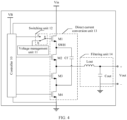
- FIG. 4 is a schematic diagram of a structure of a three-level direct current converter according to this application.
- the three-level direct current converter includes a controller 10, a voltage management unit 11, a switching unit 12, and a direct current conversion unit 13.
- the direct current conversion unit 13 includes a flying capacitor Cf and four power transistors connected in series, including a first power transistor M1, a fifth power transistor M2, a sixth power transistor M3, and a second power transistor M4.
- a drain of M1 is connected to a voltage input end Vin of the three-level direct current converter, a source of M1 is connected to a drain of M2, a source of M2 is connected to a drain of M3, a source of M3 is connected to a drain of M4, and a source of M4 is connected to a reference ground.
- the source of M1 is connected to the drain of M4 by using Cf.
- a gate of M1 is separately connected to the controller 10 and the voltage management unit 11 by using the switching unit 12, and gates of M2, M3, and M4 are all connected to the controller 10.
- the controller 10 when the three-level direct current converter starts, the controller 10 detects an input voltage of the voltage input end Vin in real time. When the input voltage starts to rise from an initial voltage (for example, 0), that is, when the three-level direct current converter starts to be powered on, the controller 10 controls the switching unit 12 to connect an output end of the voltage management unit 11 to the gate of M1. Because a first end a is connected to the gate of M1, and a second end b is connected to the output end of the voltage management unit 11, the controller 10 may control the first end a to be connected to the second end b in the switching unit 12, to connect the output end of the voltage management unit 11 to the gate of M1.
- an initial voltage for example, 0
- the controller 10 controls the switching unit 12 to connect an output end of the voltage management unit 11 to the gate of M1. Because a first end a is connected to the gate of M1, and a second end b is connected to the output end of the voltage management unit 11, the controller 10 may control the first end a to be connected to the second end
- the controller 10 controls M4 to be conducted, to output a preset voltage to the gate of M1 by using the voltage management unit 11.
- a value of the preset voltage is Vin/2 + Vgs
- Vin is the input voltage of the voltage input end Vin of the three-level direct current converter
- Vgs is a voltage difference between a gate and a source in a MOSFET.
- a charging loop of Cf may be formed by using the voltage management unit 11, M1, and M4, and Cf is precharged based on the preset voltage input by the voltage management unit 11. Then, when the input voltage of the voltage input end Vin rises to a target voltage, the controller 10 controls the first end a to be connected to a third end c in the switching unit 12, and controls M4 to be cut off.
- the existing power transistors in the three-level direct current converter are configured, to clamp a voltage of the source of M1 at Vin/2, clamp a voltage of the drain of M4 at a low level (for example, 0), that is, clamp a voltage of an upper plate of Cf at Vin/2, and clamp a voltage of a lower plate of Cf at the low level, to ensure that a voltage of Cf and voltage stress of M1 are always both Vin/2 in the entire charging process. Therefore, no additional charging circuit is required in this manner, so that circuit costs are low, and voltage stress of M1 in the entire charging process can be reduced.
- the voltage of Cf1 is 1/2 of the target voltage, charging automatically ends, without an overcharge risk. Therefore, precharging time of the flying capacitor Cf can be shortened by using a relatively large charging current.
- the direct current conversion unit 13 shown in FIG. 4 may further include a fourth power transistor.
- FIG. 5 is a schematic diagram of another structure of a three-level direct current converter according to this application.
- the direct current conversion unit 13 may further include a fourth power transistor M5, and M5 may be a metal-oxide-semiconductor field-effect transistor MOSFET.
- a drain of M5 is connected to the drain of M4, a source of M5 is connected to the source of M4, and a gate of M5 is connected to the controller 10.
- the controller 10 may further control M5 to be conducted, until the input voltage of the voltage input end Vin is the target voltage.
- a parallel charging branch circuit may be added by adding a parallel power transistor, to increase a charging current, thereby shortening precharging duration of Cf.
- the precharge duration of Cf may be alternatively shortened by increasing a quantity of power transistors connected to M1 in parallel. It should be noted that a quantity of power transistors connected to M4 in parallel and the quantity of power transistors connected to M1 in parallel are not limited in this application.
- the voltage management unit 11 shown in FIG. 4 and FIG. 5 may output a voltage of a preset voltage value Vin/2 + Vgs by using a voltage follower, a clamp circuit, or the like.
- FIG. 6 is a schematic diagram of still another structure of a three-level direct current converter according to an example for understanding this application.
- the voltage management unit 11 is a voltage follower.
- a multi-level direct current converter is an N-level direct current converter, and an input voltage of a non-inverting input end of the voltage follower is Vin * (N - 2)/(N - 1), N is 3 in the three-level direct current converter, and in this case, the input voltage of the non-inverting input end vin+ of the voltage follower is Vin/2.
- An inverting input end vin- is connected to the source of M1, and an output end vout (the output end of the voltage management unit 11) is connected to the second end b of the switching unit 12.
- a voltage of the inverting input end vin- and the voltage of the non-inverting input end vin+ of the voltage follower are equal and are both Vin/2, that is, the voltage of the source of M1 is Vin/2. Therefore, a voltage of the output end vout of the voltage follower is Vin/2 + Vgs. Because the voltage follower has a simple structure, an area is reduced, and applicability is strong.
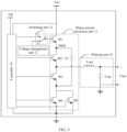
- FIG. 7 is a schematic diagram of a structure of a voltage management unit according to this application.
- the voltage management unit 11 is a clamp circuit, and includes a first resistor R1, a second resistor R2, a direct current source I, and a third power transistor M6.
- the third power transistor M6 may be a metal-oxide-semiconductor field-effect transistor MOSFET.
- One end of the first resistor R1 is connected to the voltage input end Vin of the three-level direct current converter and one end of the direct current source I, the other end of the first resistor R1 is connected to one end of the second resistor R2 and a gate of the third power transistor M6, the other end of the second resistor R2 is connected to a reference ground, the other end of the direct current source I is connected to a source of the third power transistor M6, and a drain of the third power transistor M6 is connected to a reference ground.
- the source (vout) of the third power transistor M6 is the output end of the voltage management unit 11, and the output end vout is connected to the second end b of the switching unit 12 in FIG. 5 .
- one end of the direct current source I may further provide a bias current for M6 by being connecting to another end that provides a voltage value equal to the input voltage of the voltage input end Vin of the three-level direct current converter. This is not limited in this application.
- a multi-level direct current converter is an N-level direct current converter
- a ratio between a resistance value of the first resistor and a resistance value of the second resistor is 1/(N - 2). Therefore, N is 3 in the three-level direct current converter, and in this case, a ratio between a resistance value of the first resistor R1 and a resistance value of the second resistor R2 is 1, that is, the resistance value of the first resistor R1 is equal to the resistance value of the second resistor R2.
- a voltage of the gate of M6 is Vin/2.
- the current generated by the current source I causes the voltage difference Vsg between the source and the gate of M6, and a voltage difference Vsg between a source and a gate in a PMOS is approximately equal to a voltage difference Vgs between a gate and a source in an NMOS, a voltage of the output end out of the voltage management unit 11 is Vin/2 + Vgs.
- the voltage management unit 11 may further include a switch S, and the switch S may be in an open state when the flying capacitor does not need to be precharged, thereby reducing power consumption.
- the controller 10 controls the switch S to be closed.
- the voltage of the gate of M6 is Vin/2.
- the current generated by the current source I causes the voltage difference Vsg between the source and the gate of M6. Therefore, in this case, a voltage of the output end out of the voltage management unit 11 is Vin/2 + Vgs.
- the controller 10 controls S to be open.
- the clamp circuit is easy to operate, and has high flexibility.
- the second power transistor in FIG. 3 to FIG. 7 may be indirectly controlled by the controller 10 by controlling a sequential circuit. This is not limited in this application.
- a charging loop of a flying capacitor may be formed by configuring existing power transistors in a multi-level direct current converter, to precharge the flying capacitor, without an additional charging component, so that a structure is simple, circuit costs are low, and applicability is strong.
Description
- This application relates to the field of electronic circuit technologies, and in particular, to a multi-level direct current converter and a power supply system.
- Based on a level state of a switching node, direct current/direct current converters (Direct current-Direct current converter, DC/DC converter) may be classified into two types: a two-level topology and a multi-level topology. Levels of a switching node of the two-level topology are 0 and an input voltage, and a switching node of the multilevel topology has more than two levels.
- A flying-capacitor clamped three-level direct current converter (three-level direct current converter for short) is one of DC/DC converters of the multi-level topology, and has the following feature: A half input voltage is stored by using a flying capacitor, so that a voltage of a switching node has three level states: 0, 1/2 of an input voltage, and the input voltage. Change amplitude of each time of switching of the three-level direct current converter changes to 1/2 of the input voltage, so that system performance can be improved by using a component with a low withstanding voltage and high performance. When the three-level direct current converter starts, before a power transistor starts to be switched, a voltage of the flying capacitor needs to reach 1/2 of the input voltage through precharging, to ensure normal operating of the three-level direct current converter.
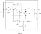
- Currently, in a three-level direct current converter shown in
FIG. 1 , a charging loop of a flying capacitor Cf is mainly formed by using current sources I_in and I_out. A specific implementation is as follows: When an upper plate of Cf is charged by using I_in, a lower plate of Cf is discharged by an equal amount by using I_out. In addition, a voltage of the lower plate of Cf is controlled by using a feedback circuit, to ensure that there is enough voltage headroom between I_in and I_out, thereby charging Cf. However, the additional current sources and feedback circuit are required in the foregoing manner. In addition, a detection circuit is further required for stopping charging of Cf after detecting that precharging of Cf is completed. Therefore, a structure is complex, and circuit costs are high.US-B-8503203 describes an apparatus for voltage conversion that includes a switched capacitor circuit, a pre-charge circuit, a voltage divider stage, and a driver stage. The switched capacitor circuit has pump capacitors to transfer energy and a steady-state operating mode and a pre-charge mode. The pre-charge circuit initially charges the pump capacitors when the switched capacitor circuit operates in the pre-charge mode. It includes a voltage divider stage having one or more nodes, each of which provides voltage at one of a corresponding one or more voltage levels, and a driver stage having one or more cascaded drivers, each of which comprises a first terminal for receiving a drive signal that depends at least in part on a voltage level at a corresponding one of the nodes, and a second terminal for coupling to a pump capacitor and to another of the drivers.
SCHAEF CHRISTOPHER ET AL: "8.1 A 93.8% Peak Efficiency, 5V-lnput, 1 0A Max II,OAD Flying Capacitor Multilevel Converter in 22nm CMOS Featuring Wide Output Voltage Range and Flying Capacitor Precharging", 2019 IEEE INTERNATIONAL SOLID- STATE CIRCUITS CONFERENCE - (ISSCC), IEEE, 17 February 2019 (2019-02-17), pages 146-148, describes a flying capacitor multilevel converter feature flying capacitor precharging. - This application provides a multi-level direct current converter and a power supply system. A charging loop of a flying capacitor may be formed by configuring existing power transistors in the multi-level direct current converter, to precharge the flying capacitor, without an additional charging component, so that a structure is simple, and circuit costs are low.
- According to a first aspect, this application provides a multi-level direct current converter as defined in
claim 1. No additional charging component is required in an entire charging process of the flying capacitor, so that a structure is simple, circuit costs are low, and applicability is strong. - With reference to the first aspect, in a first possible implementation, the voltage management unit is a voltage follower, an input voltage of a non-inverting input end of the voltage follower is determined by the input voltage of the voltage input end, an inverting input end of the voltage follower is connected to the second end of the first power transistor, and an output end of the voltage follower is used as the output end of the voltage management unit. Because the voltage follower has a simple structure, an area is reduced, and applicability is strong.
- With reference to the first aspect, in a second possible implementation, when the multi-level direct current converter is an N-level direct current converter, the input voltage of the non-inverting input end of the voltage follower is (N - 2)/(N - 1) of the input voltage of the voltage input end, where N is an integer greater than 2. Due to a concept of a virtual short circuit, the input voltage of the non-inverting input end and an input voltage of the inverting input end of the voltage follower are equal and are both (N - 2)/(N - 1) of the input voltage, and the inverting input end is connected to a source of the first power transistor. Therefore, a voltage of the source of the first power transistor is (N - 2)/(N - 1) of the input voltage in the entire charging process of the flying capacitor. In this way, it can be learned that voltage stress of the first power transistor in the entire charging process of the flying capacitor is 1/(N - 1) of the input voltage. Therefore, in this manner, voltage stress of the first power transistor in the entire charging process can be effectively reduced, thereby prolonging a service life of the first power transistor.
- With reference to the first aspect, the voltage management unit includes a first resistor, a second resistor, a direct current source, and a third power transistor. One end of the first resistor is connected to the voltage input end and one end of the direct current source, the other end of the first resistor is connected to one end of the second resistor and a first end of the third power transistor, the other end of the second resistor is connected to the reference ground, the other end of the direct current source is connected to a second end of the third power transistor, a third end of the third power transistor is connected to the reference ground, the multi-level direct current converter is an N-level direct current converter, and a ratio between a resistance value of the first resistor and a resistance value of the second resistor is 1/(N - 2). The voltage management unit is implemented in various manners and has high flexibility.
- With reference to the first aspect, in a fourth possible implementation, the third power transistor is a metal-oxide-semiconductor field-effect transistor MOSFET, and the first end, the second end, and the third end of the third power transistor are respectively a gate, a source, and a drain of the third power transistor. Due to a strong through-current capability of the MOSFET, a charging current may be appropriately increased within a tolerable current range of the power transistor in a charging process of the flying capacitor, thereby shortening precharging duration of the flying capacitor.
- With reference to the first aspect, in a fifth possible implementation, when the input voltage of the voltage input end of the multi-level direct current converter rises to a target voltage, the controller may further control the switching unit to disconnect the voltage management unit from the first power transistor and connect the controller to the third end of the first power transistor; and control the second power transistor to be cut off. Therefore, when the input voltage of the voltage input end rises to the target voltage, charging of the flying capacitor automatically ends, without an overcharge risk, so that precharging duration of the flying capacitor can be shortened by using a relatively large charging current.
- With reference to the first aspect, in a sixth possible implementation, the direct current conversion unit further includes a fourth power transistor, and the fourth power transistor is connected to the second power transistor in parallel and is connected to the controller. When the input voltage of the voltage input end starts to rise from the initial voltage, the controller may further control the fourth power transistor to be conducted, until the input voltage of the voltage input end is the target voltage. A parallel charging branch circuit may be added by adding a parallel power transistor, to increase a charging current,. In this way, precharging duration of the flying capacitor is shortened, so that applicability is strong.
- With reference to the first aspect, in a seventh possible implementation, when the multi-level direct current converter is a three-level direct current converter, the at least two power transistors further include a fifth power transistor and a sixth power transistor. The second end of the first power transistor is connected to a first end of the fifth power transistor, a second end of the fifth power transistor is connected to a first end of the sixth power transistor, a second end of the sixth power transistor is connected to the first end of the second power transistor, and a third end of the fifth power transistor and a third end of the sixth power transistor are both connected to the controller.
- With reference to the first aspect, in an eighth possible implementation, each of the at least two power transistors connected to each other in series is a metal-oxide-semiconductor field-effect transistor MOSFET. A first end of each power transistor is a drain of the power transistor, a second end of the power transistor is a source of the power transistor, and a third end of the power transistor is a gate of the power transistor. Due to a strong through-current capability of the MOSFET, a charging current may be appropriately increased within a tolerable current range of the power transistor in a charging process of the flying capacitor, thereby shortening precharging duration of the flying capacitor.
- According to a second aspect, this application provides a power supply system. The power supply system includes a photovoltaic string and the multi-level direct current converter that is provided in any one of the first aspect to the possible implementations of the first aspect and that is connected to the photovoltaic string. The multi-level direct current converter is applicable to a photovoltaic power supply scenario, and has strong applicability.
- With reference to the second aspect, in a first possible implementation, the power supply system further includes a direct current circuit breaker, and the photovoltaic string is connected to an input end of the multi-level direct current converter by using the direct current circuit breaker. The direct current circuit breaker can trigger overcurrent protection when an absolute value of a current exceeds a specific range of a rated current value, to cut off a current in a loop, thereby protecting the power supply system.
- With reference to the second aspect, in a second possible implementation, the power supply system further includes a direct current combiner box, and the photovoltaic string is connected to an input end of the multilevel direct current converter by using the direct current combiner box. Because each input of the direct current combiner box is independently equipped with a solar photovoltaic direct-current high-voltage lightning protection circuit, the direct current combiner box has a multi-level lightning protection function, to ensure that a lightning stroke does not affect normal output of a photovoltaic array, thereby improving stability of the power supply system.
- With reference to the second aspect, in a third possible implementation, the power supply system further includes an inverter, and an output end of the multi-level direct current converter is connected to the inverter.
- With reference to the second aspect, in a fourth possible implementation, the power supply system further includes a direct current bus, and the output end of the multi-level direct current converter is connected to the inverter by using the direct current bus.
- It should be understood that mutual reference may be made to implementations and beneficial effects of the plurality of aspects of this application.
-
-
FIG. 1 is a schematic diagram of a structure of a three-level direct current converter according to the conventional technology; -
FIG. 2a is a schematic diagram of an application scenario of a power supply system according to this application; -
FIG. 2b is a schematic diagram of another application scenario of a power supply system according to this application; -
FIG. 3 is a schematic diagram of a structure of a multi-level direct current converter according to this application; -
FIG. 4 is a schematic diagram of a structure of a three-level direct current converter according to this application; -
FIG. 5 is a schematic diagram of another structure of a three-level direct current converter according to this application; -
FIG. 6 is a schematic diagram of still another structure of a three-level direct current converter according to an example for understanding this application; and -
FIG. 7 is a schematic diagram of a structure of a voltage management unit according to this application. - A DC/DC converter is a commonly-used switching power supply component in an electronic system. A main function of the DC/DC converter is converting a direct current input voltage into a direct current output voltage of another electric potential, to meet a power supply requirement of an electronic system at a load end. Based on a level state of a switching node, DC/DC converters may be classified into two types: a two-level topology and a multilevel topology. Levels of a switching node of the two-level topology are 0 and an input voltage, and a switching node of the multi-level topology has more than two levels. When a DC/DC converter of the multi-level topology, namely, a multi-level direct current converter, starts, before a power transistor starts to be switched, a voltage of at least one flying capacitor in the multi-level direct current converter needs to reach a preset multiple of an input voltage through precharging, to ensure normal operating of the multi-level direct current converter, and keep stress at two ends of the power transistor within an allowable range. In an operating state, voltages of flying capacitors can be controlled by finely adjusting duty cycles. In a precharging state, the flying capacitor needs to be precharged by using different voltage precharging circuits.
- This application provides a multi-level direct current converter and a power supply system. A charging loop of a flying capacitor may be formed by configuring power transistors in the multi-level direct current converter, without an additional charging component, so that a structure is simple, and circuit costs are low.
- The multi-level direct current converter provided in this application may be adapted to different application scenarios, for example, a data center power supply scenario (to supply power to a load chip), a photovoltaic power supply scenario, an optical storage hybrid power supply scenario, and an energy storage power supply scenario. In the photovoltaic power supply scenario, a photovoltaic string is coupled to an input end of a multi-level direct current converter. In the optical storage hybrid power supply scenario, a photovoltaic string and an energy storage battery string are coupled to an input end of a multi-level direct current converter. In an energy storage power supply scenario, an energy storage battery string is coupled to an input end of a multi-level direct current converter. The following separately uses the data center power supply scenario and the photovoltaic power supply scenario as examples for description.
-
FIG. 2a is a schematic diagram of an application scenario of a power supply system according to this application. As shown inFIG. 2a , the power supply system may include a power grid, an inverter, a primary DC/DC converter, and a secondary DC/DC converter. The power grid outputs an alternating current to an input end of the inverter. The inverter obtains a direct current voltage of 48 V after inverting the alternating current output by the power grid, and outputs the direct current voltage of 48 V to an input end of the primary DC/DC converter. The primary DC/DC converter obtains a direct current voltage of 12 V after performing step-down conversion on the direct current voltage of 48 V of the input end, and outputs the direct current voltage of 12 V to an input end of the secondary DC/DC converter. The secondary DC/DC converter obtains a direct current voltage of 1 V after performing step-down conversion on the direct current voltage of 12 V of the input end, and outputs the direct current voltage of 1 V to a load chip, to supply power to the load chip. - The primary DC/DC converter or the secondary DC/DC converter herein is a multi-level direct current converter in this application. Because the multi-level direct current converter has a simple structure and low circuit costs, stability of the power supply system can be improved, and costs of the power supply system can be reduced, so that applicability is strong.
-
FIG. 2b is a schematic diagram of another application scenario of a power supply system according to this application. As shown inFIG. 2b , the power supply system may include a photovoltaic string, a DC/DC converter, and an inverter. Each photovoltaic string may include a plurality of photovoltaic components connected in series and/or connected in parallel. An input end of the DC/DC converter is connected to the photovoltaic string, and is configured to: convert, through direct current conversion, a direct current voltage generated by the photovoltaic string connected to the input end into a direct current whose voltage is a preset value, and output the direct current to the inverter. An input end of the inverter is connected to an output end of the DC/DC converter, and is configured to invert the direct current output by the DC/DC converter into an alternating current, to supply power to various types of electrical equipment such as an alternating current power grid or an alternating current load (such as a home appliance). - Optionally, the power supply system may further include a direct current combiner box (not shown in the figure). The direct current combiner box may be disposed between a plurality of photovoltaic strings and the input end of the DC/DC converter, and is configured to combine input electric energy of the plurality of photovoltaic strings and then output combined electric energy. Because each input of the direct current combiner box is independently equipped with a solar photovoltaic direct-current high-voltage lightning protection circuit, the direct current combiner box has a multi-level lightning protection function, to ensure that a lightning stroke does not affect normal output of a photovoltaic array, thereby improving stability of the power supply system.
- Optionally, the power supply system may further include a direct current circuit breaker (not shown in the figure). The direct current circuit breaker may be disposed between the photovoltaic string and the input end of the DC/DC converter, and is configured to trigger overcurrent protection when an absolute value of a current exceeds a specific range of a rated current value, to cut off a current in a loop, thereby protecting the power supply system.
- Optionally, if the power supply system includes a plurality of DC/DC converters, the power supply system may further include a direct current bus, and output ends of the DC/DC converters are connected to the input end of the inverter after being connected to the direct current bus in parallel.
- The DC/DC converter herein is a multi-level direct current converter in this application. Because the multi-level direct current converter has a simple structure and low circuit costs, stability of the power supply system can be improved, and costs of the power supply system can be reduced, so that applicability is strong.
- The foregoing merely show examples of an application scenario of the multi-level direct current converter provided in this application, but is not exhaustive. The application scenario is not limited in this application.
- The following provides, with reference to
FIG. 3 to FIG. 7 , example descriptions of an operating principle of the multi-level direct current converter provided in this application. -
FIG. 3 is a schematic diagram of a structure of a multi-level direct current converter according to this application. As shown inFIG. 3 , the multi-level direct current converter (an N-level direct current converter, where N is an integer greater than 2) includes acontroller 10, avoltage management unit 111, aswitching unit 121, and a directcurrent conversion unit 13. The directcurrent conversion unit 13 includes a flying capacitor Cf1 and at least two power transistors connected in series. The power transistors may be metal-oxide-semiconductor field-effect transistors MOSFETs. The at least two power transistors connected in series include a first power transistor M1 and a second power transistor M(2N-2). A drain of M1 is connected to a voltage input end Vin of the N-level direct current converter, a source of M1 is connected to a drain of M(2N-2) by using Cf1, and a source of M(2N-2) is connected to a reference ground. Optionally, the at least two power transistors connected in series further include power transistors M2, ..., M(N-2), M(N-1), MN, M(N+1), ..., and M(2N-3). A drain of M2 is connected to the source of M1, ..., a source of M(N-2) is connected to a drain of M(N-1), a source of M(N-1) is connected to a drain of MN, a source of MN is connected to a drain of M(N+1), ..., and a source of M(2N-3) is connected to the drain of M(2N-2). Optionally, the N-level direct current converter further includes flying capacitors Cf2 to Cf(N-2), avoltage management unit 112, ..., a voltage management unit 11(N-2), a switching unit 122, ..., and a switching unit 12(N-2). A source of M2 is connected to a drain of M(2N-3) by using Cf2, ..., and the source of M(N-2) is connected to the drain of M(N+1) by using Cf(N-2). Optionally, the N-level direct current converter further includes afiltering unit 14. Thefiltering unit 14 includes an inductor Lout and a capacitor Cout. Thefiltering unit 14 may filter a ripple in an output voltage of the N-level direct current converter, to obtain a direct current signal with a better property. It should be noted that, usually, in the N-level direct current converter, there are a total of 2N-2 power transistors connected in series, and there are a total of N-2 flying capacitors. - When the N-level direct current converter starts, before the power transistors start to be switched, capacitances of the N-2 flying capacitors in the N-level direct current converter need to reach preset multiples of an input voltage through precharging, that is, a voltage of the flying capacitor Cf1 needs to reach (Vin - (N - 2))/(N - 1) through precharging, a voltage of the flying capacitor Cf2 needs to reach (Vin - (N - 3))/(N - 1) through precharging, ..., and a voltage of the flying capacitor Cf(N-2) needs to reach Vin/(N - 1) through precharging, to ensure normal operating of the N-level direct current converter.
- In an optional implementation, when the N-level direct current converter starts, the
controller 10 detects an input voltage of the voltage input end Vin in real time. When the input voltage starts to rise from an initial voltage (for example, 0), that is, when the N-level direct current converter starts to be powered on, thecontroller 10 controls theswitching unit 121 to connect an output end of thevoltage management unit 111 to a gate of M1. Because a first end a is connected to the gate of M1, and a second end b is connected to the output end of thevoltage management unit 111, thecontroller 10 may control the first end a to be connected to the second end b in theswitching unit 121, to connect the output end of thevoltage management unit 111 to the gate of M1. In addition, thecontroller 10 controls M(2N-2) to be conducted, to output a first preset voltage to the gate of M1 by using thevoltage management unit 111. The first preset voltage is (Vin - (N - 2))/(N - 1) + Vgs, Vin is the input voltage of the voltage input end Vin of the N-level direct current converter, and Vgs is a voltage difference between a gate and a source in the MOSFET. A charging loop of Cf1 may be formed by using thevoltage management unit 111, M1, and M(2N-2), and Cf1 may be precharged based on the first preset voltage input by thevoltage management unit 111. Then, when the input voltage of the voltage input end Vin rises to a target voltage, thecontroller 10 controls the first end a to be connected to a third end c in theswitching unit 121, and controls M(2N-2) to be cut off. In this case, the voltage of Cf1 is (N - 2)/(N - 1) of the target voltage, and precharging is completed. - In an entire charging process, the existing power transistors in the N-level direct current converter are configured, to clamp a voltage of the source of M1 at (Vin - (N - 2))/(N - 1), clamp a voltage of the drain of M(2N-2) at a low level (for example, 0), that is, clamp a voltage of an upper plate of Cf1 at (Vin - (N - 2))/(N - 1), and clamp a voltage of a lower plate of Cf1 at the low level, to ensure that the voltage of Cf1 is always (Vin - (N - 2))/(N - 1) and voltage stress of M1 is always Vin - (Vin - (N - 2))/(N - 1) = Vin/(N - 1) in the entire charging process. Therefore, no additional charging circuit is required in this manner, so that circuit costs are low, and voltage stress of M1 in the entire charging process can be reduced. In addition, when the voltage of Cf1 is (N - 2)/(N - 1) of the target voltage, charging automatically ends, without an overcharge risk. Therefore, precharging time of the flying capacitor Cf1 can be shortened by using a relatively large charging current.
- Likewise, when detecting that the input voltage starts to rise from the initial voltage (for example, 0), the
controller 10 controls the switching unit 122 to connect an output end of thevoltage management unit 112 to a gate of M2. Because a first end d of the switching unit 122 is connected to the gate of M2, and a second end e is connected to the output end of thevoltage management unit 112, thecontroller 10 may control the first end d to be connected to the second end e in the switching unit 122, to connect the output end of thevoltage management unit 112 to the gate of M2. In addition, thecontroller 10 controls the power transistors M(2N-3) and M(2N-2) to be conducted, to output a second preset voltage to the gate of M2 by using thevoltage management unit 112. The second preset voltage is (Vin - (N - 3))/(N - 1) + Vgs. A charging loop of Cf2 may be formed by using thevoltage management unit 112, M2, M(2N-3), and M(2N-3), and Cf2 is precharged based on the second preset voltage input by thevoltage management unit 112. Then, when the input voltage of the voltage input end Vin rises to the target voltage, thecontroller 10 controls the first end d to be connected to a third end f in the switching unit 122, and controls M(2N-2) and M(2N-3) to be both cut off. In this case, the voltage of Cf2 is (N - 3)/(N - 1) of the target voltage, and precharging is completed. - In an entire charging process, the existing power transistors in the N-level direct current converter are configured, to clamp a voltage of the source of M2 at (Vin - (N - 3))/(N - 1), clamp a voltage of the drain of M(2N-3) at a low level (for example, 0), that is, clamp a voltage of an upper plate of Cf2 at (Vin - (N - 3))/(N - 1), and clamp a voltage of a lower plate of Cf2 at the low level, to ensure that the voltage of Cf2 is always (Vin - (N - 3))/(N - 1) and voltage stress of M2 is always (Vin - (N - 2))/(N - 1) - (Vin - (N - 3))/(N - 1) = Vin/(N - 1) in the entire charging process. Therefore, no additional charging circuit is required in this manner, so that circuit costs are low, and voltage stress of M2 in the entire charging process can be reduced. In addition, when the voltage of Cf2 is (N - 3)/(N - 1) of the target voltage, charging automatically ends, without an overcharge risk. Therefore, precharging time of the flying capacitor Cf2 can be shortened by using a relatively large charging current.
- Likewise, when detecting that the input voltage starts to rise from the initial voltage (for example, 0), the
controller 10 controls the switching unit 12(N-2) to connect an output end of thevoltage management unit 1 1(N-2) to a gate of M(N-2). Because a first end x of the switching unit 12(N-2) is connected to the gate of M(N-2), and a second end y is connected to the output end of the voltage management unit 11(N-2), thecontroller 10 may control the first end x to be connected to the second end y in the switching unit 12(N-2), to connect the output end of the voltage management unit 11(N-2) to the gate of M(N-2). In addition, thecontroller 10 controls the power transistors M(N-1), MN, ..., M(2N-3), and M(2N-2) to be all conducted, to output an (N-2)th preset voltage to the gate of M(N-2) by using the voltage management unit 11(N-2). The (N-2)th preset voltage is Vin/(N - 1) + Vgs. A charging loop of Cf(N-2) may be formed by using the voltage management unit 11(N-2), M(N-2), M(N-1), MN, M(2N-3), and M(2N-3), and Cf(N-2) is precharged based on the (N-2)th preset voltage input by the voltage management unit 11(N-2). Then, when the input voltage of the voltage input end Vin rises to the target voltage, thecontroller 10 controls the first end x to be connected to a third end z in the switching unit 12(N-2), and controls M(N-1), MN, M(2N-2), and M(2N-3) to be all cut off. In this case, the voltage of Cf(N-2) is 1/(N - 1) of the target voltage, and precharging is completed. - In an entire charging process, the existing power transistors in the N-level direct current converter are configured, to clamp a voltage of the source of M(N-2) at Vin/(N - 1), clamp a voltage of the drain of M(N+1) at a low level (for example, 0), that is, clamp a voltage of an upper plate of Cf(N-2) at Vin/(N - 1), and clamp a voltage of a lower plate of Cf(N-2) at the low level, to ensure that the voltage of Cf(N-2) is always Vin/(N - 1) and voltage stress of M(N-2) is always Vin/(N - 1) in the entire charging process. Therefore, no additional charging circuit is required in this manner, so that circuit costs are low, and voltage stress of M2 in the entire charging process can be reduced. In addition, when the voltage of Cf(N-2) is 1/(N - 1) of the target voltage, charging automatically ends, without an overcharge risk. Therefore, precharging time of the flying capacitor Cf(N-2) can be shortened by using a relatively large charging current.
- According to the foregoing manner, in a process in which the input voltage of the voltage input end Vin of the N-level direct current converter rises from the initial voltage to the target voltage, precharging processes of the N-2 flying capacitors can be completed, without an additional charging circuit, so that circuit costs are low, and applicability is strong.
- It may be understood that when the N-level direct current converter includes a plurality of flying capacitors, the flying capacitors in the N-level direct current converter are consistent in a precharging process. For ease of description, the following uses a three-level direct current converter (N is 3) as an example for description. In this case, there are four power transistors connected in series and a total of one flying capacitor in the three-level direct current converter.
-
FIG. 4 is a schematic diagram of a structure of a three-level direct current converter according to this application. As shown inFIG. 4 , the three-level direct current converter includes acontroller 10, avoltage management unit 11, a switchingunit 12, and a directcurrent conversion unit 13. The directcurrent conversion unit 13 includes a flying capacitor Cf and four power transistors connected in series, including a first power transistor M1, a fifth power transistor M2, a sixth power transistor M3, and a second power transistor M4. A drain of M1 is connected to a voltage input end Vin of the three-level direct current converter, a source of M1 is connected to a drain of M2, a source of M2 is connected to a drain of M3, a source of M3 is connected to a drain of M4, and a source of M4 is connected to a reference ground. The source of M1 is connected to the drain of M4 by using Cf. A gate of M1 is separately connected to thecontroller 10 and thevoltage management unit 11 by using theswitching unit 12, and gates of M2, M3, and M4 are all connected to thecontroller 10. - In an optional implementation, when the three-level direct current converter starts, the
controller 10 detects an input voltage of the voltage input end Vin in real time. When the input voltage starts to rise from an initial voltage (for example, 0), that is, when the three-level direct current converter starts to be powered on, thecontroller 10 controls the switchingunit 12 to connect an output end of thevoltage management unit 11 to the gate of M1. Because a first end a is connected to the gate of M1, and a second end b is connected to the output end of thevoltage management unit 11, thecontroller 10 may control the first end a to be connected to the second end b in theswitching unit 12, to connect the output end of thevoltage management unit 11 to the gate of M1. In addition, thecontroller 10 controls M4 to be conducted, to output a preset voltage to the gate of M1 by using thevoltage management unit 11. A value of the preset voltage is Vin/2 + Vgs, Vin is the input voltage of the voltage input end Vin of the three-level direct current converter, and Vgs is a voltage difference between a gate and a source in a MOSFET. A charging loop of Cf may be formed by using thevoltage management unit 11, M1, and M4, and Cf is precharged based on the preset voltage input by thevoltage management unit 11. Then, when the input voltage of the voltage input end Vin rises to a target voltage, thecontroller 10 controls the first end a to be connected to a third end c in theswitching unit 12, and controls M4 to be cut off. - In an entire charging process, the existing power transistors in the three-level direct current converter are configured, to clamp a voltage of the source of M1 at Vin/2, clamp a voltage of the drain of M4 at a low level (for example, 0), that is, clamp a voltage of an upper plate of Cf at Vin/2, and clamp a voltage of a lower plate of Cf at the low level, to ensure that a voltage of Cf and voltage stress of M1 are always both Vin/2 in the entire charging process. Therefore, no additional charging circuit is required in this manner, so that circuit costs are low, and voltage stress of M1 in the entire charging process can be reduced. In addition, when the voltage of Cf1 is 1/2 of the target voltage, charging automatically ends, without an overcharge risk. Therefore, precharging time of the flying capacitor Cf can be shortened by using a relatively large charging current.
- Further, the direct
current conversion unit 13 shown inFIG. 4 may further include a fourth power transistor. For details, refer toFIG. 5. FIG. 5 is a schematic diagram of another structure of a three-level direct current converter according to this application. As shown inFIG. 5 , the directcurrent conversion unit 13 may further include a fourth power transistor M5, and M5 may be a metal-oxide-semiconductor field-effect transistor MOSFET. A drain of M5 is connected to the drain of M4, a source of M5 is connected to the source of M4, and a gate of M5 is connected to thecontroller 10. - In an optional implementation, when detecting that the input voltage of the voltage input end Vin starts to rise from the initial voltage (for example, 0), the
controller 10 may further control M5 to be conducted, until the input voltage of the voltage input end Vin is the target voltage. It may be understood that a parallel charging branch circuit may be added by adding a parallel power transistor, to increase a charging current, thereby shortening precharging duration of Cf. In addition, the precharge duration of Cf may be alternatively shortened by increasing a quantity of power transistors connected to M1 in parallel. It should be noted that a quantity of power transistors connected to M4 in parallel and the quantity of power transistors connected to M1 in parallel are not limited in this application. - The
voltage management unit 11 shown inFIG. 4 andFIG. 5 may output a voltage of a preset voltage value Vin/2 + Vgs by using a voltage follower, a clamp circuit, or the like. - In an optional implementation,
FIG. 6 is a schematic diagram of still another structure of a three-level direct current converter according to an example for understanding this application. As shown inFIG. 6 , thevoltage management unit 11 is a voltage follower. Because a multi-level direct current converter is an N-level direct current converter, and an input voltage of a non-inverting input end of the voltage follower is Vin * (N - 2)/(N - 1), N is 3 in the three-level direct current converter, and in this case, the input voltage of the non-inverting input end vin+ of the voltage follower is Vin/2. An inverting input end vin- is connected to the source of M1, and an output end vout (the output end of the voltage management unit 11) is connected to the second end b of the switchingunit 12. According to a concept of a virtual short circuit, it can be learned that a voltage of the inverting input end vin- and the voltage of the non-inverting input end vin+ of the voltage follower are equal and are both Vin/2, that is, the voltage of the source of M1 is Vin/2. Therefore, a voltage of the output end vout of the voltage follower is Vin/2 + Vgs. Because the voltage follower has a simple structure, an area is reduced, and applicability is strong. - In another optional embodiment,
FIG. 7 is a schematic diagram of a structure of a voltage management unit according to this application. As shown inFIG. 7 , thevoltage management unit 11 is a clamp circuit, and includes a first resistor R1, a second resistor R2, a direct current source I, and a third power transistor M6. The third power transistor M6 may be a metal-oxide-semiconductor field-effect transistor MOSFET. One end of the first resistor R1 is connected to the voltage input end Vin of the three-level direct current converter and one end of the direct current source I, the other end of the first resistor R1 is connected to one end of the second resistor R2 and a gate of the third power transistor M6, the other end of the second resistor R2 is connected to a reference ground, the other end of the direct current source I is connected to a source of the third power transistor M6, and a drain of the third power transistor M6 is connected to a reference ground. The source (vout) of the third power transistor M6 is the output end of thevoltage management unit 11, and the output end vout is connected to the second end b of the switchingunit 12 inFIG. 5 . Optionally, in addition to providing a bias current (used to generate a voltage difference Vsg between the source and the gate of M6) for M6 by being connected to the voltage input end Vin of the three-level direct current converter, one end of the direct current source I may further provide a bias current for M6 by being connecting to another end that provides a voltage value equal to the input voltage of the voltage input end Vin of the three-level direct current converter. This is not limited in this application. - Because a multi-level direct current converter is an N-level direct current converter, a ratio between a resistance value of the first resistor and a resistance value of the second resistor is 1/(N - 2). Therefore, N is 3 in the three-level direct current converter, and in this case, a ratio between a resistance value of the first resistor R1 and a resistance value of the second resistor R2 is 1, that is, the resistance value of the first resistor R1 is equal to the resistance value of the second resistor R2.
- When the
voltage management unit 11 includes no switch S, because the resistance value of R1 is equal to the resistance value of R2, a voltage of the gate of M6 is Vin/2. In addition, because the current generated by the current source I causes the voltage difference Vsg between the source and the gate of M6, and a voltage difference Vsg between a source and a gate in a PMOS is approximately equal to a voltage difference Vgs between a gate and a source in an NMOS, a voltage of the output end out of thevoltage management unit 11 is Vin/2 + Vgs. - Optionally, the
voltage management unit 11 may further include a switch S, and the switch S may be in an open state when the flying capacitor does not need to be precharged, thereby reducing power consumption. - Specifically, when detecting that the input voltage of the voltage input end Vin starts to rise from the initial voltage (for example, 0), the
controller 10 controls the switch S to be closed. In this case, the voltage of the gate of M6 is Vin/2. Because the current generated by the current source I causes the voltage difference Vsg between the source and the gate of M6. Therefore, in this case, a voltage of the output end out of thevoltage management unit 11 is Vin/2 + Vgs. When the input voltage of the voltage input end Vin rises to the target voltage, thecontroller 10 controls S to be open. The clamp circuit is easy to operate, and has high flexibility. - It should be noted that, in addition to being directly controlled by the
controller 10, the second power transistor inFIG. 3 to FIG. 7 may be indirectly controlled by thecontroller 10 by controlling a sequential circuit. This is not limited in this application. - In this application, a charging loop of a flying capacitor may be formed by configuring existing power transistors in a multi-level direct current converter, to precharge the flying capacitor, without an additional charging component, so that a structure is simple, circuit costs are low, and applicability is strong.
- The foregoing descriptions are merely specific implementations of this application, but are not intended to limit the protection scope of this application. Any variation or replacement readily figured out by a person skilled in the art within the technical scope disclosed in this application shall fall within the protection scope of this application. Therefore, the protection scope of this application shall be subject to the protection scope of the claims.
Claims (11)
- A multi-level direct current converter, wherein the multi-level direct current converter comprises a direct current conversion unit (13), a switching unit (121), a voltage management unit (111), and a controller (10), wherein the direct current conversion unit comprises a flying capacitor (Cf1) and at least two power transistors (M1, M2...M(2N-2) connected in series, the at least two power transistors comprise a first power transistor (M1) and a second power transistor M(2N-2), a first end of the first power transistor is connected to a voltage input end (Vin) of the multi-level direct current converter, a second end of the first power transistor is connected to a first end of the flying capacitor and a second end of the flying capacitor is connected to a first end of the second power transistor and a second end of the second power transistor is connected to a reference ground;the switching unit is arranged to connect an output end of the voltage management unit to a third end of the first power transistor and the voltage management unit is configured to provide a preset voltage for the first power transistor; andthe controller is connected to the switching unit and a third end of the second power transistor, and is configured to: when detecting that an input voltage of the voltage input end starts to rise from an initial voltage, control the switching unit to connect the voltage management unit to the first power transistor, and control the second power transistor to be conducted;wherein the multi-level direct current converter is an N-level direct current converter;characterized in thatthe voltage management unit comprises a first resistor (R1), a second resistor (R2), a direct current source (I), and a third power transistor (M6), whereinone end of the first resistor is connected to the voltage input end and one end of the direct current source, the other end of the first resistor is connected to one end of the second resistor and a gate of the third power transistor, the other end of the second resistor is connected to the reference ground, the other end of the direct current source is connected to a second end of the third power transistor, a third end of the third power transistor is connected to the reference ground, and a ratio between a resistance value of the first resistor and a resistance value of the second resistor is 1/(N - 2), wherein N is an integer greater than 2, wherein the second end of the third power transistor is the output end of the voltage management unit.
- The multi-level direct current converter according to claim 1, wherein the third power transistor is a metal-oxide-semiconductor field-effect transistor MOSFET, and the second end, and the third end of the third power transistor are respectively a source, and a drain of the third power transistor
- The multi-level direct current converter according to claims 1 or 2, wherein the controller is further configured to: when the input voltage of the voltage input end of the multi-level direct current converter rises to a target voltage, control the switching unit to disconnect the voltage management unit from the first power transistor and connect the controller to the third end of the first power transistor; and control the second power transistor to be cut off.
- The multi-level direct current converter according to any one of claims 1 to 3, wherein the direct current conversion unit further comprises a fourth power transistor (M4), and the fourth power transistor is connected to the second power transistor in parallel and is connected to the controller; and
the controller is further configured to: when the input voltage of the voltage input end starts to rise from the initial voltage, control the fourth power transistor to be conducted, until the input voltage of the voltage input end is the target voltage. - The multi-level direct current converter according to any one of claims 1 to 4, wherein when the multi-level direct current converter is a three-level direct current converter, the at least two power transistors further comprise a fifth power transistor (M2) and a sixth power transistor (M3), wherein
the second end of the first power transistor is connected to a first end of the fifth power transistor, a second end of the fifth power transistor is connected to a first end of the sixth power transistor, a second end of the sixth power transistor is connected to the first end of the second power transistor, and a third end of the fifth power transistor and a third end of the sixth power transistor are both connected to the controller. - The multi-level direct current converter according to any one of claims 1 to 5, wherein each of the at least two power transistors connected to each other in series is a metal-oxide-semiconductor field-effect transistor MOSFET; and
a first end of each power transistor is a drain of the power transistor, a second end of the power transistor is a source of the power transistor, and a third end of the power transistor is a gate of the power transistor. - A power supply system, wherein the power supply system comprises a photovoltaic string and the multi-level direct current converter according to any one of claims 1 to 6 that is connected to the photovoltaic string.
- The power supply system according to claim 7, wherein the power supply system further comprises a direct current circuit breaker, and the photovoltaic string is connected to an input end of the multi-level direct current converter by using the direct current circuit breaker.
- The power supply system according to claim 7, wherein the power supply system further comprises a direct current combiner box, and the photovoltaic string is connected to an input end of the multi-level direct current converter by using the direct current combiner box.
- The power supply system according to any one of claims 7 to 9, wherein the power supply system further comprises an inverter, and an output end of the multi-level direct current converter is connected to the inverter.
- The power supply system according to claim 10, wherein the power supply system further comprises a direct current bus, and the output end of the multi-level direct current converter is connected to the inverter by using the direct current bus.
Applications Claiming Priority (1)
| Application Number | Priority Date | Filing Date | Title |
|---|---|---|---|
| CN202110989407.1A CN113794373B (en) | 2021-08-26 | 2021-08-26 | Multi-level direct current converter and power supply system |
Publications (2)
| Publication Number | Publication Date |
|---|---|
| EP4142131A1 EP4142131A1 (en) | 2023-03-01 |
| EP4142131B1 true EP4142131B1 (en) | 2024-02-14 |
Family
ID=78876470
Family Applications (1)
| Application Number | Title | Priority Date | Filing Date |
|---|---|---|---|
| EP22192344.4A Active EP4142131B1 (en) | 2021-08-26 | 2022-08-26 | Multi-level direct current converter and power supply system |
Country Status (3)
| Country | Link |
|---|---|
| US (1) | US20230061103A1 (en) |
| EP (1) | EP4142131B1 (en) |
| CN (1) | CN113794373B (en) |
Families Citing this family (2)
| Publication number | Priority date | Publication date | Assignee | Title |
|---|---|---|---|---|
| CN114374223A (en) * | 2021-12-21 | 2022-04-19 | 华为数字能源技术有限公司 | Resonant converter and control method thereof, MPPT (maximum power point tracking) combiner box and power supply system |
| CN114172366B (en) * | 2022-01-24 | 2023-12-15 | 澳门大学 | DC converter and electronic device |
Family Cites Families (9)
| Publication number | Priority date | Publication date | Assignee | Title |
|---|---|---|---|---|
| JP5379248B2 (en) * | 2010-02-01 | 2013-12-25 | 三菱電機株式会社 | DC / DC power converter |
| US8503203B1 (en) * | 2012-10-16 | 2013-08-06 | Arctic Sand Technologies, Inc. | Pre-charge of switched capacitor circuits with cascoded drivers |
| US10615692B2 (en) * | 2014-04-25 | 2020-04-07 | Texas Instruments Incorporated | Series capacitor buck converter having circuitry for precharging the series capacitor |
| US10447158B2 (en) * | 2016-07-01 | 2019-10-15 | Texas Instruments Incorporated | Reducing voltage rating of devices in a multilevel converter |
| CN106230253B (en) * | 2016-09-09 | 2019-05-07 | 华为技术有限公司 | Boost power translation circuit and control method |
| CN108712073B (en) * | 2018-06-08 | 2020-01-03 | 南京矽力杰半导体技术有限公司 | Three-level DC-DC converter |
| US11539294B2 (en) * | 2018-07-31 | 2022-12-27 | Dialog Semiconductor (Uk) Limited | Multi-level power converter with light load flying capacitor voltage regulation |
| US10594210B1 (en) * | 2019-04-17 | 2020-03-17 | Dialog Semiconductor (Uk) Limited | Transient response optimization for charge-pump-based two-stage power converter |
| CN212381111U (en) * | 2020-03-25 | 2021-01-19 | 上海正泰电源系统有限公司 | Three-level power conversion circuit capable of being precharged by flying capacitor |
-
2021
- 2021-08-26 CN CN202110989407.1A patent/CN113794373B/en active Active
-
2022
- 2022-08-26 EP EP22192344.4A patent/EP4142131B1/en active Active
- 2022-08-26 US US17/896,517 patent/US20230061103A1/en active Pending
Also Published As
| Publication number | Publication date |
|---|---|
| EP4142131A1 (en) | 2023-03-01 |
| CN113794373B (en) | 2024-03-01 |
| CN113794373A (en) | 2021-12-14 |
| US20230061103A1 (en) | 2023-03-02 |
Similar Documents
| Publication | Publication Date | Title |
|---|---|---|
| EP3691100B1 (en) | Switched capacitor conversion circuit, and charging control system and control method | |
| EP4142131B1 (en) | Multi-level direct current converter and power supply system | |
| EP3780322B1 (en) | Flying capacitor charging method and device | |
| US11011991B1 (en) | Regulation loop circuit | |
| US8853888B2 (en) | Multiple-input DC-DC converter | |
| Honarjoo et al. | Non‐isolated high step‐up three‐port converter with single magnetic element for photovoltaic systems | |
| US20140042815A1 (en) | Balancing, filtering and/or controlling series-connected cells | |
| Schaef et al. | A coupled-inductor multi-level ladder converter for sub-module PV power management | |
| Biswas et al. | GaN based switched capacitor three-level buck converter with cascaded synchronous bootstrap gate drive scheme | |
| US11894762B2 (en) | Direct current-direct current conversion circuit | |
| Gray et al. | A modular multilevel DC–DC converter with flying capacitor converter like properties | |
| Khan et al. | A high gain multi-port bidirectional non-isolated DC-DC converter for renewable integration | |
| US20230318340A9 (en) | Battery management circuit for a mobile device | |
| EP4054065B1 (en) | Voltage conversion circuit and power supply system | |
| Athikkal et al. | A voltage multiplier based non isolated high gain DC-DC converter for DC bus application | |
| Dastgiri et al. | A high step-up DC-DC converter with active switched LC-network and voltage-lift circuit | |
| Farooq et al. | A Three phase interleaved boost converter with L & C voltage extension mechanism | |
| WO2022211741A1 (en) | Gate driver circuit for a power supply voltage converter | |
| Haq et al. | Detachable Lithium-Ion Starter Battery and Analog Battery Management System for ICE Vehicles | |
| Hamidi et al. | A high voltage gain boost converter with the reduced number of switches using the developed switched inductor and capacitor structure | |
| Du et al. | A High-Power High-Ratio DC-DC Converter with DC Fault Blocking Capability | |
| Zheng et al. | A fixed-frequency auto-buck-boost SIMO DC-DC converter with duty-cycle redistribution and duty-predicted current control | |
| Wang et al. | Design and implementation of a battery module | |
| Naresh et al. | Comparative Analysis of Voltage Multiplier Cell Based Non-Isolated Step-Up Converters | |
| US20230155493A1 (en) | Cascade switched capacitor converter |
Legal Events
| Date | Code | Title | Description |
|---|---|---|---|
| PUAI | Public reference made under article 153(3) epc to a published international application that has entered the european phase |
Free format text: ORIGINAL CODE: 0009012 |
|
| STAA | Information on the status of an ep patent application or granted ep patent |
Free format text: STATUS: THE APPLICATION HAS BEEN PUBLISHED |
|
| AK | Designated contracting states |
Kind code of ref document: A1 Designated state(s): AL AT BE BG CH CY CZ DE DK EE ES FI FR GB GR HR HU IE IS IT LI LT LU LV MC MK MT NL NO PL PT RO RS SE SI SK SM TR |
|
| STAA | Information on the status of an ep patent application or granted ep patent |
Free format text: STATUS: REQUEST FOR EXAMINATION WAS MADE |
|
| 17P | Request for examination filed |
Effective date: 20230623 |
|
| RBV | Designated contracting states (corrected) |
Designated state(s): AL AT BE BG CH CY CZ DE DK EE ES FI FR GB GR HR HU IE IS IT LI LT LU LV MC MK MT NL NO PL PT RO RS SE SI SK SM TR |
|
| RIC1 | Information provided on ipc code assigned before grant |
Ipc: H02M 7/483 20070101ALN20230904BHEP Ipc: H02M 3/07 20060101ALI20230904BHEP Ipc: H02M 1/36 20070101AFI20230904BHEP |
|
| GRAP | Despatch of communication of intention to grant a patent |
Free format text: ORIGINAL CODE: EPIDOSNIGR1 |
|
| STAA | Information on the status of an ep patent application or granted ep patent |
Free format text: STATUS: GRANT OF PATENT IS INTENDED |
|
| RIC1 | Information provided on ipc code assigned before grant |
Ipc: H02M 7/483 20070101ALN20230920BHEP Ipc: H02M 3/07 20060101ALI20230920BHEP Ipc: H02M 1/36 20070101AFI20230920BHEP |
|
| INTG | Intention to grant announced |
Effective date: 20231013 |
|
| RIC1 | Information provided on ipc code assigned before grant |
Ipc: H02M 7/483 20070101ALN20231003BHEP Ipc: H02M 3/07 20060101ALI20231003BHEP Ipc: H02M 1/36 20070101AFI20231003BHEP |
|
| GRAS | Grant fee paid |
Free format text: ORIGINAL CODE: EPIDOSNIGR3 |
|
| GRAA | (expected) grant |
Free format text: ORIGINAL CODE: 0009210 |
|
| STAA | Information on the status of an ep patent application or granted ep patent |
Free format text: STATUS: THE PATENT HAS BEEN GRANTED |
|
| P01 | Opt-out of the competence of the unified patent court (upc) registered |
Effective date: 20231228 |
|
| AK | Designated contracting states |
Kind code of ref document: B1 Designated state(s): AL AT BE BG CH CY CZ DE DK EE ES FI FR GB GR HR HU IE IS IT LI LT LU LV MC MK MT NL NO PL PT RO RS SE SI SK SM TR |
|
| REG | Reference to a national code |
Ref country code: GB Ref legal event code: FG4D |
|
| REG | Reference to a national code |
Ref country code: CH Ref legal event code: EP |
|
| REG | Reference to a national code |
Ref country code: DE Ref legal event code: R096 Ref document number: 602022001950 Country of ref document: DE |
|
| REG | Reference to a national code |
Ref country code: IE Ref legal event code: FG4D |