EP4140745A1 - Drive device and liquid ejection head - Google Patents
Drive device and liquid ejection head Download PDFInfo
- Publication number
- EP4140745A1 EP4140745A1 EP22174765.2A EP22174765A EP4140745A1 EP 4140745 A1 EP4140745 A1 EP 4140745A1 EP 22174765 A EP22174765 A EP 22174765A EP 4140745 A1 EP4140745 A1 EP 4140745A1
- Authority
- EP
- European Patent Office
- Prior art keywords
- board
- conductors
- drive
- terminal part
- wirings
- Prior art date
- Legal status (The legal status is an assumption and is not a legal conclusion. Google has not performed a legal analysis and makes no representation as to the accuracy of the status listed.)
- Granted
Links
Images




Classifications
-
- B—PERFORMING OPERATIONS; TRANSPORTING
- B41—PRINTING; LINING MACHINES; TYPEWRITERS; STAMPS
- B41J—TYPEWRITERS; SELECTIVE PRINTING MECHANISMS, i.e. MECHANISMS PRINTING OTHERWISE THAN FROM A FORME; CORRECTION OF TYPOGRAPHICAL ERRORS
- B41J2/00—Typewriters or selective printing mechanisms characterised by the printing or marking process for which they are designed
- B41J2/005—Typewriters or selective printing mechanisms characterised by the printing or marking process for which they are designed characterised by bringing liquid or particles selectively into contact with a printing material
- B41J2/01—Ink jet
- B41J2/015—Ink jet characterised by the jet generation process
- B41J2/04—Ink jet characterised by the jet generation process generating single droplets or particles on demand
- B41J2/045—Ink jet characterised by the jet generation process generating single droplets or particles on demand by pressure, e.g. electromechanical transducers
- B41J2/04501—Control methods or devices therefor, e.g. driver circuits, control circuits
- B41J2/04581—Control methods or devices therefor, e.g. driver circuits, control circuits controlling heads based on piezoelectric elements
-
- B—PERFORMING OPERATIONS; TRANSPORTING
- B41—PRINTING; LINING MACHINES; TYPEWRITERS; STAMPS
- B41J—TYPEWRITERS; SELECTIVE PRINTING MECHANISMS, i.e. MECHANISMS PRINTING OTHERWISE THAN FROM A FORME; CORRECTION OF TYPOGRAPHICAL ERRORS
- B41J2/00—Typewriters or selective printing mechanisms characterised by the printing or marking process for which they are designed
- B41J2/005—Typewriters or selective printing mechanisms characterised by the printing or marking process for which they are designed characterised by bringing liquid or particles selectively into contact with a printing material
- B41J2/01—Ink jet
- B41J2/015—Ink jet characterised by the jet generation process
- B41J2/04—Ink jet characterised by the jet generation process generating single droplets or particles on demand
- B41J2/045—Ink jet characterised by the jet generation process generating single droplets or particles on demand by pressure, e.g. electromechanical transducers
- B41J2/04501—Control methods or devices therefor, e.g. driver circuits, control circuits
-
- B—PERFORMING OPERATIONS; TRANSPORTING
- B41—PRINTING; LINING MACHINES; TYPEWRITERS; STAMPS
- B41J—TYPEWRITERS; SELECTIVE PRINTING MECHANISMS, i.e. MECHANISMS PRINTING OTHERWISE THAN FROM A FORME; CORRECTION OF TYPOGRAPHICAL ERRORS
- B41J2/00—Typewriters or selective printing mechanisms characterised by the printing or marking process for which they are designed
- B41J2/005—Typewriters or selective printing mechanisms characterised by the printing or marking process for which they are designed characterised by bringing liquid or particles selectively into contact with a printing material
- B41J2/01—Ink jet
- B41J2/015—Ink jet characterised by the jet generation process
- B41J2/04—Ink jet characterised by the jet generation process generating single droplets or particles on demand
- B41J2/045—Ink jet characterised by the jet generation process generating single droplets or particles on demand by pressure, e.g. electromechanical transducers
- B41J2/04501—Control methods or devices therefor, e.g. driver circuits, control circuits
- B41J2/04541—Specific driving circuit
Definitions
- Embodiments described herein relate to a drive device and a liquid ejection head.
- Liquid ejection heads that eject liquids are known.
- the liquid ejection heads are mounted on, for example, an inkjet printer, a 3D printer, a dispensing device, or the like.
- the inkjet printer ejects ink droplets from an inkjet head to form an image or the like on a surface of a recording medium.
- the 3D printer ejects droplets of a modeling material from a modeling material ejection head and cures the modeling material to form a three-dimensional modeled object.
- the dispensing device ejects droplets of a sample and supplies a predetermined amount of the sample to a plurality of containers or the like.
- the liquid ejection head includes a plurality of channels for separately ejecting liquids.
- Each channel includes a nozzle for ejecting the liquid and an actuator for driving the liquid to be ejected from the nozzle.
- the actuators for the plurality of channels are formed on a common actuator board.
- a drive integrated circuit (IC) for driving these actuators such as a chip on film (COF)
- COF chip on film
- the drive IC sends a drive signal to each actuator through an individual wiring for each channel.
- the individual wirings are formed at respective terminal parts of the actuator board and the flexible printed wiring board such that a wiring width and a pitch match each other, and are connected by, for example, thermocompression bonding.
- the flexible printed wiring board equipped with the drive IC such as the COF requires a development cost
- the development cost can be reduced if a common flexible printed wiring board can be used for liquid ejection heads having different numbers of channels.
- the number of channels of drivers is increasing, and the wiring width and the pitch are made finer accordingly.
- high accuracy is required for the alignment between wirings to be connected.
- a drive device and a liquid ejection head are provided, in which conductors from a plurality of elements arranged in terminal parts on respective boards and conductors from a plurality of channels of a drive IC are connected with a high accuracy.
- the drive device includes a first board, a second board, and a relay board.
- a plurality of elements are arranged, and a plurality of first conductors configured to respectively send a drive signal to each of the plurality of elements are arranged in a terminal part.
- a drive IC configured to drive the plurality of elements is mounted, and second conductors from a plurality of channels of the drive IC are arranged in a terminal part.
- a plurality of third conductors are formed from a terminal part to be connected to the first board to a terminal part to be connected to the second board, and the third conductors each having a width larger than a pitch of the second conductors are arranged at a lower density than the second conductors in the terminal part to be connected to the second board, so that each of the first conductors configured to send the drive signal to each of the elements is connected to each of the second conductors from two or more of the channels of the drive IC.
- the drive IC is set such that outputs of two or more of the channels connected to one of the elements are the same.
- each of the third conductors is the same as a width from an outer end of one of two or more adjacent second conductors to an outer end of the other one thereof.
- a separation distance between adjacent third conductors is the same as a separation distance between adjacent second conductors.
- the third conductors in the terminal part to be connected to the second board are arranged at half the density of the second conductors in the terminal part to be connected to the relay board.
- each of the second conductors is connected to any one of the third conductors.
- the drive device is configured as a liquid ejection head comprising: an actuator board on which actuators of a plurality of channels configured to eject a liquid are arranged, and a plurality of first conductors configured to respectively send a drive signal to each of the plurality of actuators are arranged in a terminal part; a flexible board on which a drive integrated circuit (IC) configured to drive the actuators is mounted, and second conductors from a plurality of channels of the drive IC are arranged in a terminal part; and a relay flexible board on which a plurality of third conductors are formed from a terminal part to be connected to the actuator board to a terminal part to be connected to the flexible board, and the third conductors each having a width larger than a pitch of the second conductors are arranged at a lower density than the second conductors in the terminal part to be connected to the flexible board, so that each of the first conductors configured to send the drive signal to each of the actuators is connected to each of the second conductors
- the drive device is configured as a display device comprising a display board, a flexible printed wiring board, and a relay flexible printed wiring board.
- a drive device will be described in detail by taking a liquid ejection head as an example.
- the liquid ejection head is, for example, an inkjet head mounted on an inkjet printer 10 that forms an image on a recording medium.
- FIG. 1 shows a schematic configuration of the inkjet printer 10.
- the inkjet printer 10 is provided with a cassette 12 for storing sheets S that are an example of a recording medium, an upstream conveyance path 13 for the sheets S, a conveyance belt 14 for conveying the sheets S picked up from the cassette 12, a plurality of inkjet heads 100 to 103 for ejecting ink droplets toward the sheets S on the conveyance belt 14, a downstream conveyance path 15 for the sheets S, a discharge tray 16, and a control board 17 inside a housing 11.
- Image data to be printed on the sheets S is generated by, for example, a computer 200 that is an externally connected device.
- the image data generated by the computer 200 is sent to the control board 17 of the inkjet printer 10 through a cable 201 and connectors 202, 203.
- the sheets S are fed one by one by a pickup roller 204 from the cassette 12 to the upstream conveyance path 13.
- the upstream conveyance path 13 includes a feed roller pair 131, 132, and sheet guide plates 133, 134.
- the sheets S are sent to an upper surface of the conveyance belt 14 via the upstream conveyance path 13.
- An arrow 104 in the drawing indicates a conveyance path of the sheets S from the cassette 12 to the conveyance belt 14.
- the conveyance belt 14 is a net-shaped endless belt including a large number of through holes formed on a surface thereof.
- the conveyance belt 14 is rotatably supported by three rollers of a driving roller 141 and driven rollers 142, 143.
- a motor 205 rotates the conveyance belt 14 by rotating the driving roller 141.
- an arrow 105 indicates a rotation direction of the conveyance belt 14.
- the conveyance belt 14 is provided with a negative pressure container 206 on a back surface side thereof.
- the negative pressure container 206 is connected to a depressurizing fan 207.
- the fan 207 creates a negative pressure in the negative pressure container 206 by forming an air flow, and causes the sheets S to be adsorbed to and held on the upper surface of the conveyance belt 14.
- an arrow 106 indicates a flow of the air flow.
- the inkjet heads 100 to 103 which are examples of the liquid ejection heads, are arranged so as to face the sheets S adsorbed to and held on the conveyance belt 14 with a slight gap of, for example, 1 mm.
- the inkjet heads 100 to 103 eject ink droplets toward the sheets S, respectively.
- the inkjet heads 100 to 103 print an image on the sheets S that pass below.
- the inkjet heads 100 to 103 have the same structure except that colors of ink to be ejected are different.
- the colors of the ink are, for example, cyan, magenta, yellow, and black.
- the inkjet heads 100 to 103 are connected to ink tanks 315 to 318 and ink supply pressure adjusting devices 321 to 324 via ink flow paths 311 to 314, respectively.
- the ink tanks 315 to 318 are arranged above the inkjet heads 100 to 103, respectively.
- the ink supply pressure adjusting devices 321 to 324 respectively adjust the inside of the inkjet heads 100 to 103 to be a negative pressure with respect to the atmospheric pressure, for example, -1.2 kPa.
- the ink in the ink tanks 315 to 318 is supplied to the inkjet heads 100 to 103 by the ink supply pressure adjusting devices 321 to 324.
- the sheets S are sent from the conveyance belt 14 to the downstream conveyance path 15.
- the downstream conveyance path 15 includes feed roller pairs 151, 152, 153, 154, and sheet guide plates 155, 156 that define the conveyance path of the sheets S.
- the sheets S are sent from a discharge port 157 to the discharge tray 16 via the downstream conveyance path 15.
- An arrow 107 in the drawing indicates the conveyance path of the sheets S.
- the configurations of the inkjet heads 100 to 103 will be described.
- the inkjet head 100 will be described with reference to FIGS. 2 to 6 , but the inkjet heads 101 to 103 also have the same structure as the inkjet head 100.
- the inkjet head 100 includes a nozzle head unit 2 that is an example of a liquid ejection unit.
- the nozzle head unit 2 includes a nozzle plate 21, an actuator board 22, a sealing member 23 for sealing openings of pressure chambers 61 and air chambers 62 formed on the actuator board 22, and an ink supply port 24 formed in the sealing member 23.
- the ink supply port 24 is connected to the ink supply pressure adjusting device 321 of FIG. 1 via the ink flow path 311.
- the actuator board 22 as the first board is connected to a flexible printed wiring board 4 as the second board via a relay flexible printed wiring board 3 as the relay board.
- the flexible printed wiring board 4 is further connected to a printed circuit board 5 as a third board.
- the relay flexible printed wiring board 3 is an example of a relay flexible board.
- the flexible printed wiring board 4 is an example of a flexible board.
- the flexible printed wiring board 4 is equipped with an integrated circuit (IC) 41 for driving (hereinafter referred to as a drive IC) that is a driver chip.
- a drive IC 41 temporarily stores printing data sent from the control board 17 of the inkjet printer 10 via the printed circuit board 5, and outputs a drive signal for discharging ink at a predetermined timing.
- the nozzle plate 21, which is an example of a nozzle unit, is a rectangular plate made of a resin such as polyimide or a metal such as stainless steel.
- the nozzles 25 for discharging ink are arranged along a longitudinal direction (X direction) of the nozzle plate 21.
- a density of the nozzles is set, for example, within the range of 150 to 1200 dpi.
- the nozzles 25 are not limited to one row, and may be arranged in two or more rows.
- FIG. 2 shows a small number of nozzles 25 for the convenience of drawing.
- the actuator board 22 is, for example, a rectangular board made of insulating ceramics.
- a plurality of pressure chambers 61 and air chambers 62 are alternately arranged on the actuator board 22 along a first direction, for example, the X direction.
- Each of the pressure chambers 61 communicates with a respective one of the nozzles 25.
- the pressure chambers 61 communicate with the ink supply port 24 via, for example, a common ink chamber (not shown) formed on the actuator board 22 or the sealing member 23.
- each of the air chambers 62 arranged adjacent to a respective one of the pressure chambers 61 is, for example, a closed space that does not communicate with the nozzles 25 and the common ink chamber (not shown).
- the pressure chambers 61 and the air chambers 62 are formed by cutting out, for example, two piezoelectric members 26, 27 in a second direction such as a Z direction, for example, in a rectangular groove shape, the two piezoelectric members 26, 27 being laminated in directions in which polarization directions thereof are opposite to each other (for example, opposing directions) on the actuator board 22. That is, the pressure chamber 61 and the air chamber 62 adjacent thereto are partitioned by a side wall formed by the piezoelectric members 26, 27 laminated in a third direction, for example, a Y direction.
- Each of electrodes 63 is integrally formed on a bottom surface and two side surfaces of each of the pressure chambers 61.
- the electrode 63 of the pressure chamber 61 is connected to an individual wiring 64 that is a wiring electrode.
- Each of electrodes 65 is integrally formed on a bottom surface and two side surfaces of each of the air chambers 62.
- the electrode 65 of the air chamber 62 is connected to a common wiring 66 which is a wiring electrode. That is, a connection point between the electrode 63 of the pressure chamber 61 and the individual wiring 64 is one terminal of each of actuators 6.
- a connection point between the electrode 65 of the air chamber 62 and the common wiring 66 is the other terminal of each of the actuators 6.
- the electrodes 63, 65 are formed of, for example, a nickel thin film.
- the actuators 6 arranged on the actuator board 22 are examples of elements arranged on the first board.
- the individual wiring 64 is connected to a driver D (that is, a drive circuit) of the drive IC 41.
- the individual wiring 64 from each of the actuators 6 is connected to two drivers D of the drive IC 41 by adopting a wiring connection structure described in detail later. That is, an actuator 6 of #1ch is connected to the drivers D of two channels #1ch and #2ch of the drive IC 41. The same applies to actuators 6 of other channels.
- the drive IC 41 applies a drive voltage V1 as the drive signal to an actuator 6 of a channel for discharging ink. In this case, the drive IC 41 is set such that outputs of two drivers D connected to one actuator 6 are the same.
- the common wiring 66 is connected to, for example, ground (GND).
- an electric field is applied in a direction intersecting (preferably orthogonal to) polarization axes of the piezoelectric members 26, 27, and the piezoelectric members 26, 27, which are side walls of the pressure chamber 61 in the X direction, are deformed symmetrically in the X direction in a shear mode.
- each of the pressure chambers 61 for the ink is formed by being sandwiched between a pair of columnar actuators 6 using the piezoelectric members 26, 27.
- a potential difference is applied to both walls of the columnar actuator 6, that is, an inner wall and an outer wall of the pressure chamber 61, and the actuator 6 is deformed by being charged. Accordingly, a volume of the pressure chamber 61 changes, and as a result, an ink pressure in the pressure chamber 61 changes. By adjusting a magnitude and timing of this change, the ink is ejected from the nozzle 25.
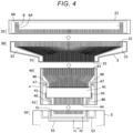
- FIGS. 4 to 6 show wiring structures of the actuator board 22, the relay flexible printed wiring board 3, the flexible printed wiring board 4, and the printed circuit board 5, separately.
- FIG. 4 is a development view before connecting the boards to each other.
- FIG. 5 is a plan view of a state in which the boards are connected.
- FIG. 6 is a side view of the state in which the boards are connected.
- a terminal part 20 of the actuator board 22 and a terminal part 30 of the relay flexible printed wiring board 3 are connected with each other.
- a terminal part 31 of the relay flexible printed wiring board 3 and a terminal part 40 of the flexible printed wiring board 4 are connected with each other.
- a terminal part 42 of the flexible printed wiring board 4 and a terminal part 50 of the printed circuit board 5 are connected with each other.
- each of the individual wirings 64 drawn from one terminal of each of the actuators 6 is formed up to the terminal part 20.
- FIGS. 4 and 5 simplify the illustration of the actuators 6 for the convenience of drawing.
- the individual wirings 64 in the terminal part 20 wirings formed with the same wiring width are arranged in parallel at equal intervals, for example.
- the individual wirings 64 are formed in a thin film form using, for example, nickel, aluminum, gold, or an alloy of these metals. In order to ensure an insulating property, for example, an insulating layer or an insulating member is provided in a region excluding the terminal part 20.
- the wiring width and wiring interval of the individual wirings 64 in the terminal part 20 are selected, for example, within the range of 10 ⁇ m to 100 ⁇ m.
- a wiring density of the individual wirings 64 in the terminal part 20 is set in terms of a resolution of 150 dpi.
- the thickness of the individual wirings 64 is, for example, 0.4 ⁇ m.
- the individual wirings 64 formed in the terminal part 20 of the actuator board 22 are an example of the first conductor from the elements formed on the first board.
- Each of the common wirings 66 is formed on a surface of the actuator board 22 along an arrangement direction of the actuators 6 and is connected to the other terminal of each of the actuators 6.
- the common wirings 66 are further formed up to the terminal part 20.
- the common wirings 66 are preferably formed from both ends of the portions formed along the arrangement direction of the actuators 6 to the terminal part 20, so that a voltage drop due to current concentration can be reduced even though a charge or discharge current is supplied to a large number of actuators 6.
- the common wirings 66 are arranged on both sides of a group of the individual wirings 64.
- the common wirings 66 are formed in a thin film form using, for example, nickel, aluminum, gold, or an alloy of these metals.
- an insulating layer or an insulating member is provided in a region excluding the terminal part 20.
- the wiring width of the common wirings 66 at the terminal part 20 is, for example, 1.5 mm.
- the thickness of the common wirings 66 is, for example, 0.4 ⁇ m.
- the relay flexible printed wiring board 3 is a flexible printed wiring board using a synthetic resin film such as polyimide.
- a synthetic resin film such as polyimide.
- individual relay wirings 32 and common relay wirings 33 extending from one terminal part 30 to the other terminal part 31 are formed separately.
- the number of the individual relay wirings 32 and the number of the common relay wirings 33 are at least the same as the number of the individual wirings 64 and the number of the common wirings 66 of the terminal part 20 of the actuator board 22, respectively. It is preferable that the wirings 32, 33 are formed on the same side (one side) of the board.
- the number, wiring width, and wiring density of individual relay wirings 32 in the terminal part 30 are preferably the same as the number, wiring width, and wiring density of the individual wirings 64 of the terminal part 20 of the actuator board 22.
- the number and wiring width of individual relay wirings 32 in the terminal part 31 do not change, but the wiring density is increased by narrowing a width of the board so as to match the width of the flexible printed wiring board 4 that is a connection counterpart.
- the wiring density is in terms of, for example, a resolution of 300 dpi.
- the individual relay wirings 32 are an individual wiring formed on the relay flexible printed wiring board 3.
- the individual relay wirings 32 formed in the terminal part 31 of the relay flexible printed wiring board 3 are an example of the third conductor formed in the relay board.
- the flexible printed wiring board 4 is a flexible printed wiring board using a synthetic resin film such as polyimide. That is, the flexible printed wiring board 4 is a board of the same type as the relay flexible printed wiring board 3.
- the drive IC 41 is, for example, a driver chip formed on a silicon semiconductor substrate.
- a preferred example of the flexible printed wiring board 4 is a chip on film (COF).
- the flexible printed wiring board 4 is provided with output wirings 43, input wirings 44, power supply wirings 45 for the voltage VI, ground wirings 46, and common wirings 47.
- Reference numeral 48 indicates a portion for alignment. It is preferable that the wirings 43 to 47 and the drive IC 41 are formed on the same surface (one side) of the board.
- the wirings 43 to 47 and the drive IC 41 are formed on one side, but when the wirings 43 to 47 and the drive IC 41 are formed on both sides, a through hole or the like is additionally formed.
- the output wirings 43 drawn out from the drive IC 41 are formed up to the terminal part 40.
- the output wirings 43 are individual wirings formed on the flexible printed wiring board 4.
- the output wirings 43 formed in the terminal part 40 of the flexible printed wiring board 4 are an example of the second conductor from channels of the drive IC 41 mounted on the second board.
- FIG. 7 is a plan view of the connection portion between the individual relay wirings 32 and the output wirings 43.
- (b) of FIG. 7 is a cross-sectional view of the connection portion between the individual relay wirings 32 and the output wirings 43.
- (c) of FIG. 7 shows an example of the wiring width and wiring interval of the individual relay wirings 32 and the output wirings 43.
- the flexible printed wiring board 4 equipped with the drive IC 41 such as the COF has an increasing number of driver channels, and by implementing fine pitch of wirings without increasing a size of the board, the output wirings 43 in the terminal part 40 form a high-density arrangement.
- the number of channels of the drive IC 41 is, for example, 1500.
- the wiring density of the output wirings 43 of the terminal part 40 is in terms of, for example, a resolution of 600 dpi.
- the wiring width of the output wirings 43 is, for example, 18 ⁇ m.
- the wiring interval is, for example, 20 ⁇ m.
- the number of channels for ejecting the ink in the nozzle head unit 2 also depends on a density of nozzles, and is, for example, 700 to 1500.
- the relay flexible printed wiring board 3 is prepared so that the common flexible printed wiring board 4 can be used even when the number of the channels for ejecting the ink (that is, the number of actuators 6) is smaller than the number of the channels of the drive IC 41.
- the wiring width of the individual relay wirings 32 of the relay flexible printed wiring board 3 is increased while the wiring density in the terminal part 31 is low according to the number of the channels for ejecting the ink and the number of the channels of the drive IC 41.
- the wiring density of the individual relay wirings 32 in the terminal part 31 of the relay flexible printed wiring board 3 is reduced to a low density of half of the wiring density of the output wirings 43 in the terminal part 40 of the flexible printed wiring board 4, and the wiring width is set to be the same as a width (separation distance) L1 from an outer end of one of two adjacent output wirings 43 to an outer end of the other one thereof.
- the wiring density is set in terms of a resolution of 300 dpi, and the wiring width is set to 56 ⁇ m. Further, the wiring width of the individual relay wiring 32 is set to 20 ⁇ m, which is the same as the wiring width of the output wiring 43.
- the individual relay wiring 32 is connected to the two adjacent output wirings 43.
- every output wiring 43 is connected to any one of the individual relay wirings 32.
- all the channels of the drive IC 41 can be used even though the number of the channels for ejecting the ink and the number of the channels of the drive IC 41 are different.
- FIG. 3 if one actuator 6 is driven with the same output of the two drivers D, a drive capacity for the actuator 6 using the piezoelectric members 26, 27 is high. The impedance is low due to the increased wiring width.
- FIG. 7 shows a configuration in which one individual relay wiring 32 is connected to two output wirings 43 as a preferable example, but the wiring width of the individual relay wiring 32 may be changed to be connected to three or more output wirings 43.
- the wiring width of the individual relay wiring 32 is preferably the same as the width from the outer end of one of the two adjacent output wirings 43 to the outer end of the other one thereof, but the wiring width of the individual relay wiring 32 can be any value as long as the width is at least larger than a pitch L2 of the two adjacent output wirings 43 (see (a) of FIG. 7 ).
- the wiring density and wiring width of the individual relay wirings 32 of the relay flexible printed wiring board 3 can be appropriately adjusted based on the number of the channels for ejecting the ink and the number of the channels of the drive IC 41. Accordingly, a common flexible printed wiring board 4 can be used for various actuator boards 22. Two or more flexible printed wiring boards 4 may be connected to one actuator board 22 on both sides or one side in parallel depending on the number of channels for ejecting the ink.
- the input wirings 44 drawn out from the drive IC 41 are formed up to the terminal part 42 on the side to be connected to the printed circuit board 5. Since the drive IC 41 can be controlled by serial communication, the number of the input wirings 44 can be smaller than the number of the output wirings 43.
- the common wirings 47 are formed from the terminal part 40 to the terminal part 42.
- the power supply wirings 45 and the ground wirings 46 are connected to the drive IC 41 separately.
- the power supply wirings 45 and the ground wirings 46 are formed up to the terminal part 42 to be connected to the printed circuit board 5 separately.
- the output wirings 43, the input wirings 44, the power supply wirings 45, the ground wirings 46, and the common wirings 47 are formed in a thin film shape using, for example, copper.
- the thickness is, for example, 8 ⁇ m.
- the wiring width and wiring interval of the output wirings 43 of the terminal part 40 are, for example, 10 ⁇ m to 30 ⁇ m.
- the wiring width and wiring interval of the input wirings 44 of the terminal part 42 are, for example, 0.15 mm.
- the wiring width of the power supply wirings 45 and the ground wirings 46 is, for example, 0.4 mm.
- the wiring width of the common wirings 47 is, for example, 0.85 mm.
- the printed circuit board 5 is a hard through-hole board in which an epoxy resin layer containing glass fibers and a copper wiring layer are laminated in a plurality of layers.
- the terminal part 50 is provided with output wirings 51, a power supply wiring 52, and a ground wiring 53 separately.
- Each of the output wirings 51 is connected to a respective one of the input wirings 44 of the flexible printed wiring board 4.
- the power supply wiring 52 is connected to the power supply wirings 45 of the flexible printed wiring board 4.
- the ground wiring 53 is connected to the ground wirings 46 and the common wirings 47 of the flexible printed wiring board 4.
- a signal for selectively driving each actuator 6 from the control board 17 of the inkjet printer 10 is sent to the output wirings 51.
- the drive voltage V1 is applied to the power supply wiring 52.
- the ground wiring 53 is connected to the ground (GND) by, for example, the control board 17 of the inkjet printer 10.
- the terminal part 20 of the actuator board 22 and the terminal part 30 of the relay flexible printed wiring board 3 are connected via an anisotropic conductive film (ACF) 7 as a preferable example.
- ACF anisotropic conductive film
- the wirings of the terminal parts 20, 30 are connected all at once by arranging the terminal part 20 of the actuator board 22 and the terminal part 30 of the relay flexible printed wiring board 3 so as to face each other, interposing the ACF 7 between the terminal parts 20, 30, and then, for example, thermocompression-bonding the ACF 7 and the terminal parts 20, 30 with a thermocompression bonding tool.
- each of the individual wirings 64 can be electrically connected to a respective one of the individual relay wirings 32
- each of the common wirings 66 can be electrically connected to a respective one of the common relay wirings 33.
- the terminal part 31 of the relay flexible printed wiring board 3 and the terminal part 40 of the flexible printed wiring board 4 are also connected via the ACF 7.
- the terminal part 42 of the flexible printed wiring board 4 and the terminal part 50 of the printed circuit board 5 are also connected via the ACF 7.
- the inkjet head 100 is not limited to shear mode type actuators 6 in which the pressure chambers 61 and the air chambers 62 are alternately arranged. Shear mode and share wall type actuators 6 in which the pressure chambers 61 are continuously arranged may also be used. Drop-on-demand piezo type actuators or the like may also be used.
- the inkjet head 100 of the inkjet printer 10 is described as an example of the liquid ejection head, but the liquid ejection head may be a modeling material ejection head of a 3D printer or a sample ejection head of a dispensing device.
- a drive device according to a second embodiment will be described by taking a display device 8 such as a liquid crystal display and an organic electroluminescence display as an example.
- a display device 8 such as a liquid crystal display and an organic electroluminescence display
- the same components as those in the first embodiment are denoted by the same reference numerals, and detailed descriptions thereof will be omitted.
- the display device 8 includes a display board 80 such as a liquid crystal board. Although not shown, a plurality of elements such as liquid crystal elements are arranged in the X direction and the Y direction on the display board 80.
- the display board 80 is connected to the flexible printed wiring board 4 via the relay flexible printed wiring board 3.
- the flexible printed wiring board 4 is further connected to the printed circuit board 5. Elements of the display board 80 are driven by the drive IC 41 mounted on the flexible printed wiring board 4.
- the relay flexible printed wiring board 3 is interposed between the boards 22, 80 on which the elements such as the actuators 6 are arranged and the flexible printed wiring board 4 on which the drive IC 41 is mounted, and the wiring density and wiring width of the individual relay wirings 32 of the relay flexible printed wiring board 3 are adjusted, so that the individual wirings 64 from the plurality of elements and the output wirings 43 from the plurality of channels of the drive IC 41 can be connected with high accuracy via the individual relay wirings 32.
Landscapes
- Particle Formation And Scattering Control In Inkjet Printers (AREA)
Abstract
Description
- Embodiments described herein relate to a drive device and a liquid ejection head.
- Liquid ejection heads that eject liquids are known. The liquid ejection heads are mounted on, for example, an inkjet printer, a 3D printer, a dispensing device, or the like. The inkjet printer ejects ink droplets from an inkjet head to form an image or the like on a surface of a recording medium. The 3D printer ejects droplets of a modeling material from a modeling material ejection head and cures the modeling material to form a three-dimensional modeled object. The dispensing device ejects droplets of a sample and supplies a predetermined amount of the sample to a plurality of containers or the like.
- The liquid ejection head includes a plurality of channels for separately ejecting liquids. Each channel includes a nozzle for ejecting the liquid and an actuator for driving the liquid to be ejected from the nozzle. The actuators for the plurality of channels are formed on a common actuator board. A drive integrated circuit (IC) for driving these actuators, such as a chip on film (COF), is mounted on a flexible printed wiring board and is used. When driving the actuators, the drive IC sends a drive signal to each actuator through an individual wiring for each channel. The individual wirings are formed at respective terminal parts of the actuator board and the flexible printed wiring board such that a wiring width and a pitch match each other, and are connected by, for example, thermocompression bonding.
- Since the flexible printed wiring board equipped with the drive IC such as the COF requires a development cost, the development cost can be reduced if a common flexible printed wiring board can be used for liquid ejection heads having different numbers of channels. However, in the flexible printed wiring board equipped with the drive IC such as the COF, the number of channels of drivers is increasing, and the wiring width and the pitch are made finer accordingly. Thus, in the mounting process of the actuator board and the flexible printed wiring board, high accuracy is required for the alignment between wirings to be connected.
-
-
FIG. 1 is an overall configuration diagram of an inkjet printer provided with an inkjet head according to a first embodiment; -
FIG. 2 is a perspective view of the inkjet head; -
FIG. 3 is a cross-sectional view of an actuator of the inkjet head; -
FIG. 4 is a development view before connecting an actuator board, a relay flexible printed wiring board, a flexible printed wiring board, and a printed circuit board to each other; -
FIG. 5 is a plan view of a state in which the actuator board, the relay flexible printed wiring board, the flexible printed wiring board, and the printed circuit board are connected to each other; -
FIG. 6 is a side view of the state in which the actuator board, the relay flexible printed wiring board, the flexible printed wiring board, and the printed circuit board are connected to each other; -
FIG. 7 is an enlarged view of a wiring connection portion between the relay flexible printed wiring board and the flexible printed wiring board; -
FIGS. 8A and 8B are enlarged views of the wiring connection portion between the relay flexible printed wiring board and the flexible printed wiring board; and -
FIG. 9 is a perspective view of a display device according to a second embodiment. - In general, according to one embodiment, a drive device and a liquid ejection head are provided, in which conductors from a plurality of elements arranged in terminal parts on respective boards and conductors from a plurality of channels of a drive IC are connected with a high accuracy.
- The drive device according to the embodiment includes a first board, a second board, and a relay board. On the first board, a plurality of elements are arranged, and a plurality of first conductors configured to respectively send a drive signal to each of the plurality of elements are arranged in a terminal part. On the second board, a drive IC configured to drive the plurality of elements is mounted, and second conductors from a plurality of channels of the drive IC are arranged in a terminal part. On the relay board, a plurality of third conductors are formed from a terminal part to be connected to the first board to a terminal part to be connected to the second board, and the third conductors each having a width larger than a pitch of the second conductors are arranged at a lower density than the second conductors in the terminal part to be connected to the second board, so that each of the first conductors configured to send the drive signal to each of the elements is connected to each of the second conductors from two or more of the channels of the drive IC.
- Preferably, the drive IC is set such that outputs of two or more of the channels connected to one of the elements are the same.
- Preferably, the width of each of the third conductors is the same as a width from an outer end of one of two or more adjacent second conductors to an outer end of the other one thereof.
- Preferably, a separation distance between adjacent third conductors is the same as a separation distance between adjacent second conductors.
- Preferably, the third conductors in the terminal part to be connected to the second board are arranged at half the density of the second conductors in the terminal part to be connected to the relay board.
- Preferably, each of the second conductors is connected to any one of the third conductors.
- According to an embodiment, the drive device is configured as a liquid ejection head comprising: an actuator board on which actuators of a plurality of channels configured to eject a liquid are arranged, and a plurality of first conductors configured to respectively send a drive signal to each of the plurality of actuators are arranged in a terminal part; a flexible board on which a drive integrated circuit (IC) configured to drive the actuators is mounted, and second conductors from a plurality of channels of the drive IC are arranged in a terminal part; and a relay flexible board on which a plurality of third conductors are formed from a terminal part to be connected to the actuator board to a terminal part to be connected to the flexible board, and the third conductors each having a width larger than a pitch of the second conductors are arranged at a lower density than the second conductors in the terminal part to be connected to the flexible board, so that each of the first conductors configured to send the drive signal to each of the actuators is connected to each of the second conductors from two or more of the channels of the drive IC.
- According to an embodiment, the drive device is configured as a display device comprising a display board, a flexible printed wiring board, and a relay flexible printed wiring board.
- Hereinafter, a drive device and a liquid ejection head according to embodiments will be described in detail with reference to the accompanying drawings. In the drawings, the same configurations are denoted by the same reference numerals.
- A drive device according to a first embodiment will be described in detail by taking a liquid ejection head as an example. The liquid ejection head is, for example, an inkjet head mounted on an
inkjet printer 10 that forms an image on a recording medium.FIG. 1 shows a schematic configuration of theinkjet printer 10. Theinkjet printer 10 is provided with acassette 12 for storing sheets S that are an example of a recording medium, anupstream conveyance path 13 for the sheets S, aconveyance belt 14 for conveying the sheets S picked up from thecassette 12, a plurality ofinkjet heads 100 to 103 for ejecting ink droplets toward the sheets S on theconveyance belt 14, adownstream conveyance path 15 for the sheets S, adischarge tray 16, and acontrol board 17 inside ahousing 11. Anoperation unit 18, which is a user interface, is arranged on an upper side of thehousing 11. - Image data to be printed on the sheets S is generated by, for example, a
computer 200 that is an externally connected device. The image data generated by thecomputer 200 is sent to thecontrol board 17 of theinkjet printer 10 through acable 201 andconnectors - The sheets S are fed one by one by a
pickup roller 204 from thecassette 12 to theupstream conveyance path 13. Theupstream conveyance path 13 includes afeed roller pair sheet guide plates conveyance belt 14 via theupstream conveyance path 13. An arrow 104 in the drawing indicates a conveyance path of the sheets S from thecassette 12 to theconveyance belt 14. - The
conveyance belt 14 is a net-shaped endless belt including a large number of through holes formed on a surface thereof. Theconveyance belt 14 is rotatably supported by three rollers of adriving roller 141 and drivenrollers motor 205 rotates theconveyance belt 14 by rotating thedriving roller 141. In the drawing, anarrow 105 indicates a rotation direction of theconveyance belt 14. Theconveyance belt 14 is provided with anegative pressure container 206 on a back surface side thereof. Thenegative pressure container 206 is connected to a depressurizingfan 207. Thefan 207 creates a negative pressure in thenegative pressure container 206 by forming an air flow, and causes the sheets S to be adsorbed to and held on the upper surface of theconveyance belt 14. In the drawing, anarrow 106 indicates a flow of the air flow. - The
inkjet heads 100 to 103, which are examples of the liquid ejection heads, are arranged so as to face the sheets S adsorbed to and held on theconveyance belt 14 with a slight gap of, for example, 1 mm. The inkjet heads 100 to 103 eject ink droplets toward the sheets S, respectively. The inkjet heads 100 to 103 print an image on the sheets S that pass below. The inkjet heads 100 to 103 have the same structure except that colors of ink to be ejected are different. The colors of the ink are, for example, cyan, magenta, yellow, and black. - The inkjet heads 100 to 103 are connected to
ink tanks 315 to 318 and ink supplypressure adjusting devices 321 to 324 viaink flow paths 311 to 314, respectively. Theink tanks 315 to 318 are arranged above the inkjet heads 100 to 103, respectively. To prevent ink from leaking from nozzles 25 (seeFIG. 2 ) of the inkjet heads 100 to 103 during standby, the ink supplypressure adjusting devices 321 to 324 respectively adjust the inside of the inkjet heads 100 to 103 to be a negative pressure with respect to the atmospheric pressure, for example, -1.2 kPa. When an image is formed, the ink in theink tanks 315 to 318 is supplied to the inkjet heads 100 to 103 by the ink supplypressure adjusting devices 321 to 324. - After forming the image, the sheets S are sent from the
conveyance belt 14 to thedownstream conveyance path 15. Thedownstream conveyance path 15 includes feed roller pairs 151, 152, 153, 154, andsheet guide plates discharge port 157 to thedischarge tray 16 via thedownstream conveyance path 15. Anarrow 107 in the drawing indicates the conveyance path of the sheets S. - Subsequently, the configurations of the inkjet heads 100 to 103 will be described. Hereinafter, the
inkjet head 100 will be described with reference toFIGS. 2 to 6 , but the inkjet heads 101 to 103 also have the same structure as theinkjet head 100. - As shown in
FIG. 2 , theinkjet head 100 includes a nozzle head unit 2 that is an example of a liquid ejection unit. The nozzle head unit 2 includes anozzle plate 21, anactuator board 22, a sealingmember 23 for sealing openings ofpressure chambers 61 andair chambers 62 formed on theactuator board 22, and anink supply port 24 formed in the sealingmember 23. Theink supply port 24 is connected to the ink supplypressure adjusting device 321 ofFIG. 1 via theink flow path 311. - The
actuator board 22 as the first board is connected to a flexible printedwiring board 4 as the second board via a relay flexible printedwiring board 3 as the relay board. The flexible printedwiring board 4 is further connected to a printedcircuit board 5 as a third board. The relay flexible printedwiring board 3 is an example of a relay flexible board. The flexible printedwiring board 4 is an example of a flexible board. - The flexible printed
wiring board 4 is equipped with an integrated circuit (IC) 41 for driving (hereinafter referred to as a drive IC) that is a driver chip. Thedrive IC 41 temporarily stores printing data sent from thecontrol board 17 of theinkjet printer 10 via the printedcircuit board 5, and outputs a drive signal for discharging ink at a predetermined timing. - The
nozzle plate 21, which is an example of a nozzle unit, is a rectangular plate made of a resin such as polyimide or a metal such as stainless steel. Thenozzles 25 for discharging ink are arranged along a longitudinal direction (X direction) of thenozzle plate 21. A density of the nozzles is set, for example, within the range of 150 to 1200 dpi. Thenozzles 25 are not limited to one row, and may be arranged in two or more rows.FIG. 2 shows a small number ofnozzles 25 for the convenience of drawing. - The
actuator board 22 is, for example, a rectangular board made of insulating ceramics. A plurality ofpressure chambers 61 andair chambers 62 are alternately arranged on theactuator board 22 along a first direction, for example, the X direction. Each of thepressure chambers 61 communicates with a respective one of thenozzles 25. Thepressure chambers 61 communicate with theink supply port 24 via, for example, a common ink chamber (not shown) formed on theactuator board 22 or the sealingmember 23. On the other hand, each of theair chambers 62 arranged adjacent to a respective one of thepressure chambers 61 is, for example, a closed space that does not communicate with thenozzles 25 and the common ink chamber (not shown). - As shown in
FIG. 3 , thepressure chambers 61 and theair chambers 62 are formed by cutting out, for example, twopiezoelectric members piezoelectric members actuator board 22. That is, thepressure chamber 61 and theair chamber 62 adjacent thereto are partitioned by a side wall formed by thepiezoelectric members - Each of
electrodes 63 is integrally formed on a bottom surface and two side surfaces of each of thepressure chambers 61. Theelectrode 63 of thepressure chamber 61 is connected to anindividual wiring 64 that is a wiring electrode. Each ofelectrodes 65 is integrally formed on a bottom surface and two side surfaces of each of theair chambers 62. Theelectrode 65 of theair chamber 62 is connected to acommon wiring 66 which is a wiring electrode. That is, a connection point between theelectrode 63 of thepressure chamber 61 and theindividual wiring 64 is one terminal of each ofactuators 6. A connection point between theelectrode 65 of theair chamber 62 and thecommon wiring 66 is the other terminal of each of theactuators 6. Theelectrodes actuators 6 arranged on theactuator board 22 are examples of elements arranged on the first board. - The
individual wiring 64 is connected to a driver D (that is, a drive circuit) of thedrive IC 41. In this case, theindividual wiring 64 from each of theactuators 6 is connected to two drivers D of thedrive IC 41 by adopting a wiring connection structure described in detail later. That is, anactuator 6 of #1ch is connected to the drivers D of two channels #1ch and #2ch of thedrive IC 41. The same applies to actuators 6 of other channels. Thedrive IC 41 applies a drive voltage V1 as the drive signal to anactuator 6 of a channel for discharging ink. In this case, thedrive IC 41 is set such that outputs of two drivers D connected to oneactuator 6 are the same. On the other hand, thecommon wiring 66 is connected to, for example, ground (GND). With this configuration, in theactuator 6 to which the drive voltage V1 is applied, an electric field is applied in a direction intersecting (preferably orthogonal to) polarization axes of thepiezoelectric members piezoelectric members pressure chamber 61 in the X direction, are deformed symmetrically in the X direction in a shear mode. - That is, each of the
pressure chambers 61 for the ink is formed by being sandwiched between a pair ofcolumnar actuators 6 using thepiezoelectric members columnar actuator 6, that is, an inner wall and an outer wall of thepressure chamber 61, and theactuator 6 is deformed by being charged. Accordingly, a volume of thepressure chamber 61 changes, and as a result, an ink pressure in thepressure chamber 61 changes. By adjusting a magnitude and timing of this change, the ink is ejected from thenozzle 25. -
FIGS. 4 to 6 show wiring structures of theactuator board 22, the relay flexible printedwiring board 3, the flexible printedwiring board 4, and the printedcircuit board 5, separately.FIG. 4 is a development view before connecting the boards to each other.FIG. 5 is a plan view of a state in which the boards are connected.FIG. 6 is a side view of the state in which the boards are connected. Aterminal part 20 of theactuator board 22 and aterminal part 30 of the relay flexible printedwiring board 3 are connected with each other. Aterminal part 31 of the relay flexible printedwiring board 3 and aterminal part 40 of the flexible printedwiring board 4 are connected with each other. Aterminal part 42 of the flexible printedwiring board 4 and aterminal part 50 of the printedcircuit board 5 are connected with each other. - On the
actuator board 22, each of theindividual wirings 64 drawn from one terminal of each of theactuators 6 is formed up to theterminal part 20.FIGS. 4 and5 simplify the illustration of theactuators 6 for the convenience of drawing. As theindividual wirings 64 in theterminal part 20, wirings formed with the same wiring width are arranged in parallel at equal intervals, for example. Theindividual wirings 64 are formed in a thin film form using, for example, nickel, aluminum, gold, or an alloy of these metals. In order to ensure an insulating property, for example, an insulating layer or an insulating member is provided in a region excluding theterminal part 20. The wiring width and wiring interval of theindividual wirings 64 in theterminal part 20 are selected, for example, within the range of 10 µm to 100 µm. As an example, a wiring density of theindividual wirings 64 in theterminal part 20 is set in terms of a resolution of 150 dpi. The thickness of theindividual wirings 64 is, for example, 0.4 µm. Theindividual wirings 64 formed in theterminal part 20 of theactuator board 22 are an example of the first conductor from the elements formed on the first board. - Each of the
common wirings 66 is formed on a surface of theactuator board 22 along an arrangement direction of theactuators 6 and is connected to the other terminal of each of theactuators 6. Thecommon wirings 66 are further formed up to theterminal part 20. In this case, thecommon wirings 66 are preferably formed from both ends of the portions formed along the arrangement direction of theactuators 6 to theterminal part 20, so that a voltage drop due to current concentration can be reduced even though a charge or discharge current is supplied to a large number ofactuators 6. Also in theterminal part 20, thecommon wirings 66 are arranged on both sides of a group of theindividual wirings 64. Thecommon wirings 66 are formed in a thin film form using, for example, nickel, aluminum, gold, or an alloy of these metals. In order to ensure the insulating property, for example, an insulating layer or an insulating member is provided in a region excluding theterminal part 20. The wiring width of thecommon wirings 66 at theterminal part 20 is, for example, 1.5 mm. The thickness of thecommon wirings 66 is, for example, 0.4 µm. - The relay flexible printed
wiring board 3 is a flexible printed wiring board using a synthetic resin film such as polyimide. On the relay flexible printedwiring board 3, individual relay wirings 32 andcommon relay wirings 33 extending from oneterminal part 30 to the otherterminal part 31 are formed separately. The number of the individual relay wirings 32 and the number of thecommon relay wirings 33 are at least the same as the number of theindividual wirings 64 and the number of thecommon wirings 66 of theterminal part 20 of theactuator board 22, respectively. It is preferable that thewirings terminal part 30 are preferably the same as the number, wiring width, and wiring density of theindividual wirings 64 of theterminal part 20 of theactuator board 22. On the other hand, the number and wiring width of individual relay wirings 32 in theterminal part 31 do not change, but the wiring density is increased by narrowing a width of the board so as to match the width of the flexible printedwiring board 4 that is a connection counterpart. The wiring density is in terms of, for example, a resolution of 300 dpi. The individual relay wirings 32 are an individual wiring formed on the relay flexible printedwiring board 3. Thus, the individual relay wirings 32 formed in theterminal part 31 of the relay flexible printedwiring board 3 are an example of the third conductor formed in the relay board. - The flexible printed
wiring board 4 is a flexible printed wiring board using a synthetic resin film such as polyimide. That is, the flexible printedwiring board 4 is a board of the same type as the relay flexible printedwiring board 3. Thedrive IC 41 is, for example, a driver chip formed on a silicon semiconductor substrate. A preferred example of the flexible printedwiring board 4 is a chip on film (COF). The flexible printedwiring board 4 is provided withoutput wirings 43, input wirings 44,power supply wirings 45 for the voltage VI, ground wirings 46, andcommon wirings 47.Reference numeral 48 indicates a portion for alignment. It is preferable that thewirings 43 to 47 and thedrive IC 41 are formed on the same surface (one side) of the board. In the case of COF, thewirings 43 to 47 and thedrive IC 41 are formed on one side, but when thewirings 43 to 47 and thedrive IC 41 are formed on both sides, a through hole or the like is additionally formed. The output wirings 43 drawn out from thedrive IC 41 are formed up to theterminal part 40. The output wirings 43 are individual wirings formed on the flexible printedwiring board 4. Thus, theoutput wirings 43 formed in theterminal part 40 of the flexible printedwiring board 4 are an example of the second conductor from channels of thedrive IC 41 mounted on the second board. - Here, the connection between the individual relay wirings 32 of the relay flexible printed
wiring board 3 and the output wirings 43 of the flexible printedwiring board 4 will be described in more detail with reference toFIG. 7. (a) ofFIG. 7 is a plan view of the connection portion between the individual relay wirings 32 and theoutput wirings 43.(b) ofFIG. 7 is a cross-sectional view of the connection portion between the individual relay wirings 32 and theoutput wirings 43.(c) ofFIG. 7 shows an example of the wiring width and wiring interval of the individual relay wirings 32 and theoutput wirings 43. As described above, the flexible printedwiring board 4 equipped with thedrive IC 41 such as the COF has an increasing number of driver channels, and by implementing fine pitch of wirings without increasing a size of the board, theoutput wirings 43 in theterminal part 40 form a high-density arrangement. The number of channels of thedrive IC 41 is, for example, 1500. The wiring density of the output wirings 43 of theterminal part 40 is in terms of, for example, a resolution of 600 dpi. The wiring width of theoutput wirings 43 is, for example, 18 µm. The wiring interval is, for example, 20 µm. - On the other hand, the number of channels for ejecting the ink in the nozzle head unit 2 also depends on a density of nozzles, and is, for example, 700 to 1500. As described above, the relay flexible printed
wiring board 3 is prepared so that the common flexible printedwiring board 4 can be used even when the number of the channels for ejecting the ink (that is, the number of actuators 6) is smaller than the number of the channels of thedrive IC 41. - For more details, the wiring width of the individual relay wirings 32 of the relay flexible printed
wiring board 3 is increased while the wiring density in theterminal part 31 is low according to the number of the channels for ejecting the ink and the number of the channels of thedrive IC 41. As a preferable example in (a) to (c) ofFIG. 7 , the wiring density of the individual relay wirings 32 in theterminal part 31 of the relay flexible printedwiring board 3 is reduced to a low density of half of the wiring density of theoutput wirings 43 in theterminal part 40 of the flexible printedwiring board 4, and the wiring width is set to be the same as a width (separation distance) L1 from an outer end of one of two adjacent output wirings 43 to an outer end of the other one thereof. That is, the wiring density is set in terms of a resolution of 300 dpi, and the wiring width is set to 56 µm. Further, the wiring width of theindividual relay wiring 32 is set to 20 µm, which is the same as the wiring width of theoutput wiring 43. - By setting in this way, when the
terminal parts individual relay wiring 32 is connected to the twoadjacent output wirings 43. In addition, as a desirable form, everyoutput wiring 43 is connected to any one of theindividual relay wirings 32. As a result, all the channels of thedrive IC 41 can be used even though the number of the channels for ejecting the ink and the number of the channels of thedrive IC 41 are different. As shown inFIG. 3 , if oneactuator 6 is driven with the same output of the two drivers D, a drive capacity for theactuator 6 using thepiezoelectric members - As shown in
FIG. 8A , even though the wiring density in theterminal part 31 of the relay flexible printedwiring board 3 is 300 dpi, a usage rate of the channels of thedrive IC 41 is halved when the wiring width of theindividual relay wiring 32 is 18 µm, which is the same as that of theoutput wiring 43. The drive capacity for charging or discharging theactuators 6 may be insufficient. As shown inFIG. 8B , when the wiring density in theterminal part 31 is set to 600 dpi and a wiring density on theterminal part 30 side is set to 300 dpi by connecting two individual relay wirings 32 to one, the usage rate of the channels of thedrive IC 41 is improved, but a high alignment accuracy of the wirings is required in a mounting process for connecting boards to each other. Since the wiring width of theindividual relay wiring 32 is narrow, the impedance becomes high, and the drive capacity for charging or discharging theactuators 6 may be limited. -
FIG. 7 shows a configuration in which oneindividual relay wiring 32 is connected to twooutput wirings 43 as a preferable example, but the wiring width of theindividual relay wiring 32 may be changed to be connected to three ormore output wirings 43. The wiring width of theindividual relay wiring 32 is preferably the same as the width from the outer end of one of the two adjacent output wirings 43 to the outer end of the other one thereof, but the wiring width of theindividual relay wiring 32 can be any value as long as the width is at least larger than a pitch L2 of the two adjacent output wirings 43 (see (a) ofFIG. 7 ). The wiring density and wiring width of the individual relay wirings 32 of the relay flexible printedwiring board 3 can be appropriately adjusted based on the number of the channels for ejecting the ink and the number of the channels of thedrive IC 41. Accordingly, a common flexible printedwiring board 4 can be used forvarious actuator boards 22. Two or more flexible printedwiring boards 4 may be connected to oneactuator board 22 on both sides or one side in parallel depending on the number of channels for ejecting the ink. - Returning to
FIGS. 4 to 6 , the input wirings 44 drawn out from thedrive IC 41 are formed up to theterminal part 42 on the side to be connected to the printedcircuit board 5. Since thedrive IC 41 can be controlled by serial communication, the number of the input wirings 44 can be smaller than the number of theoutput wirings 43. Thecommon wirings 47 are formed from theterminal part 40 to theterminal part 42. - The
power supply wirings 45 and the ground wirings 46 are connected to thedrive IC 41 separately. Thepower supply wirings 45 and the ground wirings 46 are formed up to theterminal part 42 to be connected to the printedcircuit board 5 separately. The output wirings 43, theinput wirings 44, thepower supply wirings 45, the ground wirings 46, and thecommon wirings 47 are formed in a thin film shape using, for example, copper. The thickness is, for example, 8 µm. The wiring width and wiring interval of the output wirings 43 of theterminal part 40 are, for example, 10 µm to 30 µm. The wiring width and wiring interval of the input wirings 44 of theterminal part 42 are, for example, 0.15 mm. The wiring width of thepower supply wirings 45 and the ground wirings 46 is, for example, 0.4 mm. The wiring width of thecommon wirings 47 is, for example, 0.85 mm. - The printed
circuit board 5 is a hard through-hole board in which an epoxy resin layer containing glass fibers and a copper wiring layer are laminated in a plurality of layers. Theterminal part 50 is provided withoutput wirings 51, apower supply wiring 52, and aground wiring 53 separately. Each of theoutput wirings 51 is connected to a respective one of the input wirings 44 of the flexible printedwiring board 4. Thepower supply wiring 52 is connected to the power supply wirings 45 of the flexible printedwiring board 4. Theground wiring 53 is connected to the ground wirings 46 and thecommon wirings 47 of the flexible printedwiring board 4. A signal for selectively driving eachactuator 6 from thecontrol board 17 of theinkjet printer 10 is sent to theoutput wirings 51. The drive voltage V1 is applied to thepower supply wiring 52. Theground wiring 53 is connected to the ground (GND) by, for example, thecontrol board 17 of theinkjet printer 10. - As shown in
FIG. 6 , theterminal part 20 of theactuator board 22 and theterminal part 30 of the relay flexible printedwiring board 3 are connected via an anisotropic conductive film (ACF) 7 as a preferable example. Specifically, the wirings of theterminal parts terminal part 20 of theactuator board 22 and theterminal part 30 of the relay flexible printedwiring board 3 so as to face each other, interposing theACF 7 between theterminal parts ACF 7 and theterminal parts individual wirings 64 can be electrically connected to a respective one of the individual relay wirings 32, and each of thecommon wirings 66 can be electrically connected to a respective one of thecommon relay wirings 33. - The
terminal part 31 of the relay flexible printedwiring board 3 and theterminal part 40 of the flexible printedwiring board 4 are also connected via theACF 7. Theterminal part 42 of the flexible printedwiring board 4 and theterminal part 50 of the printedcircuit board 5 are also connected via theACF 7. - The
inkjet head 100 is not limited to shearmode type actuators 6 in which thepressure chambers 61 and theair chambers 62 are alternately arranged. Shear mode and sharewall type actuators 6 in which thepressure chambers 61 are continuously arranged may also be used. Drop-on-demand piezo type actuators or the like may also be used. - In the above-described embodiment, the
inkjet head 100 of theinkjet printer 10 is described as an example of the liquid ejection head, but the liquid ejection head may be a modeling material ejection head of a 3D printer or a sample ejection head of a dispensing device. - Next, a drive device according to a second embodiment will be described by taking a
display device 8 such as a liquid crystal display and an organic electroluminescence display as an example. However, the same components as those in the first embodiment are denoted by the same reference numerals, and detailed descriptions thereof will be omitted. - The
display device 8 includes adisplay board 80 such as a liquid crystal board. Although not shown, a plurality of elements such as liquid crystal elements are arranged in the X direction and the Y direction on thedisplay board 80. Thedisplay board 80 is connected to the flexible printedwiring board 4 via the relay flexible printedwiring board 3. The flexible printedwiring board 4 is further connected to the printedcircuit board 5. Elements of thedisplay board 80 are driven by thedrive IC 41 mounted on the flexible printedwiring board 4. - According to either one of the above embodiments, the relay flexible printed
wiring board 3 is interposed between theboards actuators 6 are arranged and the flexible printedwiring board 4 on which thedrive IC 41 is mounted, and the wiring density and wiring width of the individual relay wirings 32 of the relay flexible printedwiring board 3 are adjusted, so that theindividual wirings 64 from the plurality of elements and the output wirings 43 from the plurality of channels of thedrive IC 41 can be connected with high accuracy via theindividual relay wirings 32. - The embodiments have been presented as examples and are not intended to limit the scope of the disclosure. The novel embodiments can be implemented in other various forms, and various omissions, replacements, and changes can be made without departing from the spirit of the disclosure. The embodiments and modifications thereof are included in the scope and gist of the disclosure, and are also included in the invention described in the scope of the claims and an equivalent scope thereof.
Claims (8)
- A drive device comprising:a first board (22) on which a plurality of elements (6) are arranged, and a plurality of first conductors (64) configured to respectively send a drive signal to each of the plurality of elements are arranged in a terminal part (20);a second board (4) on which a drive integrated circuit (IC) (41) configured to drive the plurality of elements is mounted, and second conductors (43) from a plurality of channels of the drive IC are arranged in a terminal part (40); anda relay board (3) on which a plurality of third conductors (32) are formed from a terminal part (30) to be connected to the first board (22) to a terminal part (31) to be connected to the second board (4), and the third conductors (32) each having a width larger than a pitch of the second conductors (43) are arranged at a lower density than the second conductors (43) in the terminal part (31) to be connected to the second board (4), so that each of the first conductors (64) configured to send the drive signal to each of the elements (6) is connected to each of the second conductors (43) from two or more of the channels of the drive IC (41).
- The drive device according to claim 1, wherein the drive IC (41) is set such that outputs of two or more of the channels connected to one of the elements (6) are the same.
- The drive device according to claim 1 or 2, wherein the width of each of the third conductors (32) is the same as a width from an outer end of one of two or more adjacent second conductors (43) to an outer end of the other one thereof.
- The drive device according to any one of claims 1 to 3, wherein a separation distance between adjacent third conductors (32) is the same as a separation distance between adjacent second conductors (43).
- The drive device according to any one of claims 1 to 4, wherein the third conductors (32) in the terminal part (31) to be connected to the second board (4) are arranged at half the density of the second conductors (43) in the terminal part (40) to be connected to the relay board (3).
- The drive device according to any one of claims 1 to 5, wherein each of the second conductors (43) is connected to any one of the third conductors (32).
- The drive device according to any one of claims 1 to 6 configured as a liquid ejection head (100) comprising:the first board configured as an actuator board on which actuators of a plurality of channels configured to eject a liquid are arranged, and a plurality of first conductors configured to respectively send a drive signal to each of the plurality of actuators are arranged in a terminal part;the second board configured as a flexible board on which a drive integrated circuit (IC) configured to drive the actuators is mounted, and second conductors from a plurality of channels of the drive IC are arranged in a terminal part; andthe relay board configured as a relay flexible board on which a plurality of third conductors are formed from a terminal part to be connected to the actuator board to a terminal part to be connected to the flexible board, and the third conductors each having a width larger than a pitch of the second conductors are arranged at a lower density than the second conductors in the terminal part to be connected to the flexible board, so that each of the first conductors configured to send the drive signal to each of the actuators is connected to each of the second conductors from two or more of the channels of the drive IC.
- The drive device according to any one of claims 1 to 7 configured as a display device (8), comprising the first board configured as a display board (80), the second board configured as a flexible printed wiring board (4), and the relay board configured as a relay flexible printed wiring board (3).
Applications Claiming Priority (1)
| Application Number | Priority Date | Filing Date | Title |
|---|---|---|---|
| JP2021136796A JP7636297B2 (en) | 2021-08-25 | 2021-08-25 | Driving device, liquid ejection head |
Publications (2)
| Publication Number | Publication Date |
|---|---|
| EP4140745A1 true EP4140745A1 (en) | 2023-03-01 |
| EP4140745B1 EP4140745B1 (en) | 2024-07-31 |
Family
ID=81841953
Family Applications (1)
| Application Number | Title | Priority Date | Filing Date |
|---|---|---|---|
| EP22174765.2A Active EP4140745B1 (en) | 2021-08-25 | 2022-05-23 | Inkjet head comprising a drive device |
Country Status (3)
| Country | Link |
|---|---|
| EP (1) | EP4140745B1 (en) |
| JP (1) | JP7636297B2 (en) |
| CN (1) | CN115891430B (en) |
Families Citing this family (1)
| Publication number | Priority date | Publication date | Assignee | Title |
|---|---|---|---|---|
| JP7658894B2 (en) * | 2021-12-28 | 2025-04-08 | 京セラ株式会社 | Liquid ejection head and recording apparatus |
Citations (6)
| Publication number | Priority date | Publication date | Assignee | Title |
|---|---|---|---|---|
| US20040169545A1 (en) * | 2002-01-28 | 2004-09-02 | Masahiko Aiba | Capactive load driving circuit, capacitive load driving method, and apparatus using the same |
| EP2130678A1 (en) * | 2008-06-04 | 2009-12-09 | SII Printek Inc | Head chip, liquid jet head, liquid jet recording device, and method of manufacturing the head chip |
| EP2390095A1 (en) * | 2010-05-31 | 2011-11-30 | SII Printek Inc | Liquid jet head and liquid jet apparatus |
| US20180147845A1 (en) * | 2016-11-25 | 2018-05-31 | Toshiba Tec Kabushiki Kaisha | Liquid jetting device |
| US20180272703A1 (en) * | 2017-03-24 | 2018-09-27 | Toshiba Tec Kabushiki Kaisha | Liquid ejecting head and liquid ejecting device |
| EP3528603A1 (en) * | 2018-02-20 | 2019-08-21 | Toshiba Tec Kabushiki Kaisha | Ink jet head and ink jet printer |
Family Cites Families (10)
| Publication number | Priority date | Publication date | Assignee | Title |
|---|---|---|---|---|
| JPH0712703B2 (en) * | 1988-12-09 | 1995-02-15 | 松下電器産業株式会社 | Thermal head |
| US7658470B1 (en) * | 2005-04-28 | 2010-02-09 | Hewlett-Packard Development Company, L.P. | Method of using a flexible circuit |
| JP3864987B2 (en) | 2006-01-19 | 2007-01-10 | ブラザー工業株式会社 | Flexible wiring board connection structure |
| JP4976364B2 (en) * | 2008-12-04 | 2012-07-18 | エスアイアイ・プリンテック株式会社 | Liquid ejecting head and liquid ejecting apparatus |
| JP5941645B2 (en) | 2011-09-27 | 2016-06-29 | エスアイアイ・プリンテック株式会社 | Liquid ejecting head and liquid ejecting apparatus |
| CN105518961B (en) * | 2013-07-24 | 2018-04-13 | 4233999加拿大股份有限公司 | For driving the controllable constant current source integrated circuit of closely spaced array |
| JP2015150826A (en) * | 2014-02-18 | 2015-08-24 | セイコーエプソン株式会社 | Wiring mounting structure, liquid ejecting head, and liquid ejecting apparatus |
| JP6869673B2 (en) * | 2016-09-15 | 2021-05-12 | 東芝テック株式会社 | Inkjet head |
| JP7483318B2 (en) * | 2018-01-31 | 2024-05-15 | セイコーエプソン株式会社 | Printhead |
| CN109278409B (en) | 2018-08-16 | 2019-07-23 | 西安微电子技术研究所 | A kind of MEMS piezoelectricity printing head component integrated morphology |
-
2021
- 2021-08-25 JP JP2021136796A patent/JP7636297B2/en active Active
-
2022
- 2022-04-22 CN CN202210429078.XA patent/CN115891430B/en active Active
- 2022-05-23 EP EP22174765.2A patent/EP4140745B1/en active Active
Patent Citations (6)
| Publication number | Priority date | Publication date | Assignee | Title |
|---|---|---|---|---|
| US20040169545A1 (en) * | 2002-01-28 | 2004-09-02 | Masahiko Aiba | Capactive load driving circuit, capacitive load driving method, and apparatus using the same |
| EP2130678A1 (en) * | 2008-06-04 | 2009-12-09 | SII Printek Inc | Head chip, liquid jet head, liquid jet recording device, and method of manufacturing the head chip |
| EP2390095A1 (en) * | 2010-05-31 | 2011-11-30 | SII Printek Inc | Liquid jet head and liquid jet apparatus |
| US20180147845A1 (en) * | 2016-11-25 | 2018-05-31 | Toshiba Tec Kabushiki Kaisha | Liquid jetting device |
| US20180272703A1 (en) * | 2017-03-24 | 2018-09-27 | Toshiba Tec Kabushiki Kaisha | Liquid ejecting head and liquid ejecting device |
| EP3528603A1 (en) * | 2018-02-20 | 2019-08-21 | Toshiba Tec Kabushiki Kaisha | Ink jet head and ink jet printer |
Also Published As
| Publication number | Publication date |
|---|---|
| EP4140745B1 (en) | 2024-07-31 |
| JP7636297B2 (en) | 2025-02-26 |
| CN115891430B (en) | 2025-07-25 |
| CN115891430A (en) | 2023-04-04 |
| JP2023031359A (en) | 2023-03-09 |
Similar Documents
| Publication | Publication Date | Title |
|---|---|---|
| CN102218919B (en) | Liquid ejection head, liquid ejection unit and liquid ejection device | |
| US8807707B2 (en) | Liquid jet head and liquid jet apparatus | |
| JP7009925B2 (en) | Head unit | |
| US20110292115A1 (en) | Liquid jet head and liquid jet apparatus | |
| JP2016088084A (en) | Liquid injection head, liquid injection head unit and liquid injection device | |
| CN109720091B (en) | head unit | |
| US9682557B2 (en) | Liquid ejecting head, liquid ejecting head unit, and liquid ejecting apparatus | |
| US9919516B2 (en) | Liquid ejecting head and liquid ejecting apparatus | |
| CN109130489B (en) | Liquid ejecting head and liquid ejecting apparatus | |
| CN101961955B (en) | Liquid spray head and liquid spray device | |
| EP4140745B1 (en) | Inkjet head comprising a drive device | |
| US10814628B2 (en) | Liquid ejecting head, liquid ejecting apparatus, and wiring substrate | |
| EP4230421B1 (en) | A liquid ejection head and a method of measuring electrical resistance in a liquid ejection head | |
| EP4303012A1 (en) | Liquid ejection head | |
| CN114851711B (en) | Liquid ejection head | |
| JP7636225B2 (en) | Film wiring board for driving liquid ejection head, liquid ejection head | |
| JP7461760B2 (en) | Liquid ejection device and method for manufacturing the same | |
| JP2012218251A (en) | Liquid jet head, and liquid jet apparatus | |
| EP4570504A1 (en) | Liquid ejection head | |
| JP7717584B2 (en) | Driving device, liquid ejection head | |
| JP2025052840A (en) | Liquid ejection head | |
| US11427000B2 (en) | Liquid discharge head | |
| JP2025052839A (en) | Liquid ejection head | |
| JP2024106211A (en) | Liquid ejection head | |
| CN118358260A (en) | Liquid spray head |
Legal Events
| Date | Code | Title | Description |
|---|---|---|---|
| PUAI | Public reference made under article 153(3) epc to a published international application that has entered the european phase |
Free format text: ORIGINAL CODE: 0009012 |
|
| STAA | Information on the status of an ep patent application or granted ep patent |
Free format text: STATUS: THE APPLICATION HAS BEEN PUBLISHED |
|
| AK | Designated contracting states |
Kind code of ref document: A1 Designated state(s): AL AT BE BG CH CY CZ DE DK EE ES FI FR GB GR HR HU IE IS IT LI LT LU LV MC MK MT NL NO PL PT RO RS SE SI SK SM TR |
|
| STAA | Information on the status of an ep patent application or granted ep patent |
Free format text: STATUS: REQUEST FOR EXAMINATION WAS MADE |
|
| 17P | Request for examination filed |
Effective date: 20230901 |
|
| RBV | Designated contracting states (corrected) |
Designated state(s): AL AT BE BG CH CY CZ DE DK EE ES FI FR GB GR HR HU IE IS IT LI LT LU LV MC MK MT NL NO PL PT RO RS SE SI SK SM TR |
|
| GRAP | Despatch of communication of intention to grant a patent |
Free format text: ORIGINAL CODE: EPIDOSNIGR1 |
|
| STAA | Information on the status of an ep patent application or granted ep patent |
Free format text: STATUS: GRANT OF PATENT IS INTENDED |
|
| INTG | Intention to grant announced |
Effective date: 20240307 |
|
| GRAS | Grant fee paid |
Free format text: ORIGINAL CODE: EPIDOSNIGR3 |
|
| GRAA | (expected) grant |
Free format text: ORIGINAL CODE: 0009210 |
|
| STAA | Information on the status of an ep patent application or granted ep patent |
Free format text: STATUS: THE PATENT HAS BEEN GRANTED |
|
| AK | Designated contracting states |
Kind code of ref document: B1 Designated state(s): AL AT BE BG CH CY CZ DE DK EE ES FI FR GB GR HR HU IE IS IT LI LT LU LV MC MK MT NL NO PL PT RO RS SE SI SK SM TR |
|
| REG | Reference to a national code |
Ref country code: CH Ref legal event code: EP Ref country code: GB Ref legal event code: FG4D |
|
| REG | Reference to a national code |
Ref country code: DE Ref legal event code: R096 Ref document number: 602022004897 Country of ref document: DE |
|
| REG | Reference to a national code |
Ref country code: IE Ref legal event code: FG4D |
|
| REG | Reference to a national code |
Ref country code: DE Ref legal event code: R081 Ref document number: 602022004897 Country of ref document: DE Owner name: RISO TECHNOLOGIES CORPORATION, JP Free format text: FORMER OWNER: TOSHIBA TEC KABUSHIKI KAISHA, TOKYO, JP |
|
| RAP2 | Party data changed (patent owner data changed or rights of a patent transferred) |
Owner name: RISO TECHNOLOGIES CORPORATION |
|
| REG | Reference to a national code |
Ref country code: GB Ref legal event code: 732E Free format text: REGISTERED BETWEEN 20241003 AND 20241009 |
|
| REG | Reference to a national code |
Ref country code: LT Ref legal event code: MG9D |
|
| REG | Reference to a national code |
Ref country code: NL Ref legal event code: MP Effective date: 20240731 |
|
| PG25 | Lapsed in a contracting state [announced via postgrant information from national office to epo] |
Ref country code: PT Free format text: LAPSE BECAUSE OF FAILURE TO SUBMIT A TRANSLATION OF THE DESCRIPTION OR TO PAY THE FEE WITHIN THE PRESCRIBED TIME-LIMIT Effective date: 20241202 |
|
| REG | Reference to a national code |
Ref country code: AT Ref legal event code: MK05 Ref document number: 1708122 Country of ref document: AT Kind code of ref document: T Effective date: 20240731 |
|
| PG25 | Lapsed in a contracting state [announced via postgrant information from national office to epo] |
Ref country code: PT Free format text: LAPSE BECAUSE OF FAILURE TO SUBMIT A TRANSLATION OF THE DESCRIPTION OR TO PAY THE FEE WITHIN THE PRESCRIBED TIME-LIMIT Effective date: 20241202 |
|
| PG25 | Lapsed in a contracting state [announced via postgrant information from national office to epo] |
Ref country code: NO Free format text: LAPSE BECAUSE OF FAILURE TO SUBMIT A TRANSLATION OF THE DESCRIPTION OR TO PAY THE FEE WITHIN THE PRESCRIBED TIME-LIMIT Effective date: 20241031 |
|
| PG25 | Lapsed in a contracting state [announced via postgrant information from national office to epo] |
Ref country code: FI Free format text: LAPSE BECAUSE OF FAILURE TO SUBMIT A TRANSLATION OF THE DESCRIPTION OR TO PAY THE FEE WITHIN THE PRESCRIBED TIME-LIMIT Effective date: 20240731 Ref country code: NL Free format text: LAPSE BECAUSE OF FAILURE TO SUBMIT A TRANSLATION OF THE DESCRIPTION OR TO PAY THE FEE WITHIN THE PRESCRIBED TIME-LIMIT Effective date: 20240731 Ref country code: PL Free format text: LAPSE BECAUSE OF FAILURE TO SUBMIT A TRANSLATION OF THE DESCRIPTION OR TO PAY THE FEE WITHIN THE PRESCRIBED TIME-LIMIT Effective date: 20240731 Ref country code: GR Free format text: LAPSE BECAUSE OF FAILURE TO SUBMIT A TRANSLATION OF THE DESCRIPTION OR TO PAY THE FEE WITHIN THE PRESCRIBED TIME-LIMIT Effective date: 20241101 |
|
| PG25 | Lapsed in a contracting state [announced via postgrant information from national office to epo] |
Ref country code: BG Free format text: LAPSE BECAUSE OF FAILURE TO SUBMIT A TRANSLATION OF THE DESCRIPTION OR TO PAY THE FEE WITHIN THE PRESCRIBED TIME-LIMIT Effective date: 20240731 |
|
| PG25 | Lapsed in a contracting state [announced via postgrant information from national office to epo] |
Ref country code: LV Free format text: LAPSE BECAUSE OF FAILURE TO SUBMIT A TRANSLATION OF THE DESCRIPTION OR TO PAY THE FEE WITHIN THE PRESCRIBED TIME-LIMIT Effective date: 20240731 |
|
| PG25 | Lapsed in a contracting state [announced via postgrant information from national office to epo] |
Ref country code: AT Free format text: LAPSE BECAUSE OF FAILURE TO SUBMIT A TRANSLATION OF THE DESCRIPTION OR TO PAY THE FEE WITHIN THE PRESCRIBED TIME-LIMIT Effective date: 20240731 Ref country code: IS Free format text: LAPSE BECAUSE OF FAILURE TO SUBMIT A TRANSLATION OF THE DESCRIPTION OR TO PAY THE FEE WITHIN THE PRESCRIBED TIME-LIMIT Effective date: 20241130 |
|
| PG25 | Lapsed in a contracting state [announced via postgrant information from national office to epo] |
Ref country code: HR Free format text: LAPSE BECAUSE OF FAILURE TO SUBMIT A TRANSLATION OF THE DESCRIPTION OR TO PAY THE FEE WITHIN THE PRESCRIBED TIME-LIMIT Effective date: 20240731 |
|
| PG25 | Lapsed in a contracting state [announced via postgrant information from national office to epo] |
Ref country code: ES Free format text: LAPSE BECAUSE OF FAILURE TO SUBMIT A TRANSLATION OF THE DESCRIPTION OR TO PAY THE FEE WITHIN THE PRESCRIBED TIME-LIMIT Effective date: 20240731 Ref country code: RS Free format text: LAPSE BECAUSE OF FAILURE TO SUBMIT A TRANSLATION OF THE DESCRIPTION OR TO PAY THE FEE WITHIN THE PRESCRIBED TIME-LIMIT Effective date: 20241031 |
|
| PG25 | Lapsed in a contracting state [announced via postgrant information from national office to epo] |
Ref country code: RS Free format text: LAPSE BECAUSE OF FAILURE TO SUBMIT A TRANSLATION OF THE DESCRIPTION OR TO PAY THE FEE WITHIN THE PRESCRIBED TIME-LIMIT Effective date: 20241031 Ref country code: PL Free format text: LAPSE BECAUSE OF FAILURE TO SUBMIT A TRANSLATION OF THE DESCRIPTION OR TO PAY THE FEE WITHIN THE PRESCRIBED TIME-LIMIT Effective date: 20240731 Ref country code: NO Free format text: LAPSE BECAUSE OF FAILURE TO SUBMIT A TRANSLATION OF THE DESCRIPTION OR TO PAY THE FEE WITHIN THE PRESCRIBED TIME-LIMIT Effective date: 20241031 Ref country code: NL Free format text: LAPSE BECAUSE OF FAILURE TO SUBMIT A TRANSLATION OF THE DESCRIPTION OR TO PAY THE FEE WITHIN THE PRESCRIBED TIME-LIMIT Effective date: 20240731 Ref country code: LV Free format text: LAPSE BECAUSE OF FAILURE TO SUBMIT A TRANSLATION OF THE DESCRIPTION OR TO PAY THE FEE WITHIN THE PRESCRIBED TIME-LIMIT Effective date: 20240731 Ref country code: IS Free format text: LAPSE BECAUSE OF FAILURE TO SUBMIT A TRANSLATION OF THE DESCRIPTION OR TO PAY THE FEE WITHIN THE PRESCRIBED TIME-LIMIT Effective date: 20241130 Ref country code: HR Free format text: LAPSE BECAUSE OF FAILURE TO SUBMIT A TRANSLATION OF THE DESCRIPTION OR TO PAY THE FEE WITHIN THE PRESCRIBED TIME-LIMIT Effective date: 20240731 Ref country code: GR Free format text: LAPSE BECAUSE OF FAILURE TO SUBMIT A TRANSLATION OF THE DESCRIPTION OR TO PAY THE FEE WITHIN THE PRESCRIBED TIME-LIMIT Effective date: 20241101 Ref country code: FI Free format text: LAPSE BECAUSE OF FAILURE TO SUBMIT A TRANSLATION OF THE DESCRIPTION OR TO PAY THE FEE WITHIN THE PRESCRIBED TIME-LIMIT Effective date: 20240731 Ref country code: ES Free format text: LAPSE BECAUSE OF FAILURE TO SUBMIT A TRANSLATION OF THE DESCRIPTION OR TO PAY THE FEE WITHIN THE PRESCRIBED TIME-LIMIT Effective date: 20240731 Ref country code: BG Free format text: LAPSE BECAUSE OF FAILURE TO SUBMIT A TRANSLATION OF THE DESCRIPTION OR TO PAY THE FEE WITHIN THE PRESCRIBED TIME-LIMIT Effective date: 20240731 Ref country code: AT Free format text: LAPSE BECAUSE OF FAILURE TO SUBMIT A TRANSLATION OF THE DESCRIPTION OR TO PAY THE FEE WITHIN THE PRESCRIBED TIME-LIMIT Effective date: 20240731 |
|
| P01 | Opt-out of the competence of the unified patent court (upc) registered |
Free format text: CASE NUMBER: APP_68129/2024 Effective date: 20241226 |
|
| P02 | Opt-out of the competence of the unified patent court (upc) changed |
Free format text: CASE NUMBER: APP_68500/2024 Effective date: 20241227 |
|
| PG25 | Lapsed in a contracting state [announced via postgrant information from national office to epo] |
Ref country code: SM Free format text: LAPSE BECAUSE OF FAILURE TO SUBMIT A TRANSLATION OF THE DESCRIPTION OR TO PAY THE FEE WITHIN THE PRESCRIBED TIME-LIMIT Effective date: 20240731 Ref country code: RO Free format text: LAPSE BECAUSE OF FAILURE TO SUBMIT A TRANSLATION OF THE DESCRIPTION OR TO PAY THE FEE WITHIN THE PRESCRIBED TIME-LIMIT Effective date: 20240731 Ref country code: DK Free format text: LAPSE BECAUSE OF FAILURE TO SUBMIT A TRANSLATION OF THE DESCRIPTION OR TO PAY THE FEE WITHIN THE PRESCRIBED TIME-LIMIT Effective date: 20240731 |
|
| PG25 | Lapsed in a contracting state [announced via postgrant information from national office to epo] |
Ref country code: EE Free format text: LAPSE BECAUSE OF FAILURE TO SUBMIT A TRANSLATION OF THE DESCRIPTION OR TO PAY THE FEE WITHIN THE PRESCRIBED TIME-LIMIT Effective date: 20240731 |
|
| PG25 | Lapsed in a contracting state [announced via postgrant information from national office to epo] |
Ref country code: CZ Free format text: LAPSE BECAUSE OF FAILURE TO SUBMIT A TRANSLATION OF THE DESCRIPTION OR TO PAY THE FEE WITHIN THE PRESCRIBED TIME-LIMIT Effective date: 20240731 |
|
| PG25 | Lapsed in a contracting state [announced via postgrant information from national office to epo] |
Ref country code: IT Free format text: LAPSE BECAUSE OF FAILURE TO SUBMIT A TRANSLATION OF THE DESCRIPTION OR TO PAY THE FEE WITHIN THE PRESCRIBED TIME-LIMIT Effective date: 20240731 Ref country code: SK Free format text: LAPSE BECAUSE OF FAILURE TO SUBMIT A TRANSLATION OF THE DESCRIPTION OR TO PAY THE FEE WITHIN THE PRESCRIBED TIME-LIMIT Effective date: 20240731 |
|
| REG | Reference to a national code |
Ref country code: DE Ref legal event code: R097 Ref document number: 602022004897 Country of ref document: DE |
|
| PLBE | No opposition filed within time limit |
Free format text: ORIGINAL CODE: 0009261 |
|
| STAA | Information on the status of an ep patent application or granted ep patent |
Free format text: STATUS: NO OPPOSITION FILED WITHIN TIME LIMIT |
|
| 26N | No opposition filed |
Effective date: 20250501 |
|
| PG25 | Lapsed in a contracting state [announced via postgrant information from national office to epo] |
Ref country code: SE Free format text: LAPSE BECAUSE OF FAILURE TO SUBMIT A TRANSLATION OF THE DESCRIPTION OR TO PAY THE FEE WITHIN THE PRESCRIBED TIME-LIMIT Effective date: 20240731 |
|
| REG | Reference to a national code |
Ref country code: CH Ref legal event code: H13 Free format text: ST27 STATUS EVENT CODE: U-0-0-H10-H13 (AS PROVIDED BY THE NATIONAL OFFICE) Effective date: 20251223 |
|
| PG25 | Lapsed in a contracting state [announced via postgrant information from national office to epo] |
Ref country code: LU Free format text: LAPSE BECAUSE OF NON-PAYMENT OF DUE FEES Effective date: 20250523 |
|
| PG25 | Lapsed in a contracting state [announced via postgrant information from national office to epo] |
Ref country code: CH Free format text: LAPSE BECAUSE OF NON-PAYMENT OF DUE FEES Effective date: 20250531 |
|
| REG | Reference to a national code |
Ref country code: BE Ref legal event code: MM Effective date: 20250531 |
|
| PG25 | Lapsed in a contracting state [announced via postgrant information from national office to epo] |
Ref country code: MC Free format text: LAPSE BECAUSE OF FAILURE TO SUBMIT A TRANSLATION OF THE DESCRIPTION OR TO PAY THE FEE WITHIN THE PRESCRIBED TIME-LIMIT Effective date: 20240731 |
|
| PGFP | Annual fee paid to national office [announced via postgrant information from national office to epo] |
Ref country code: GB Payment date: 20260324 Year of fee payment: 5 |
|
| PG25 | Lapsed in a contracting state [announced via postgrant information from national office to epo] |
Ref country code: IE Free format text: LAPSE BECAUSE OF NON-PAYMENT OF DUE FEES Effective date: 20250523 |
|
| PG25 | Lapsed in a contracting state [announced via postgrant information from national office to epo] |
Ref country code: BE Free format text: LAPSE BECAUSE OF NON-PAYMENT OF DUE FEES Effective date: 20250531 |
|
| PG25 | Lapsed in a contracting state [announced via postgrant information from national office to epo] |
Ref country code: LT Free format text: LAPSE BECAUSE OF FAILURE TO SUBMIT A TRANSLATION OF THE DESCRIPTION OR TO PAY THE FEE WITHIN THE PRESCRIBED TIME-LIMIT Effective date: 20240731 |
|
| PGFP | Annual fee paid to national office [announced via postgrant information from national office to epo] |
Ref country code: DE Payment date: 20260520 Year of fee payment: 5 |
|
| PGFP | Annual fee paid to national office [announced via postgrant information from national office to epo] |
Ref country code: FR Payment date: 20260522 Year of fee payment: 5 |
|
| PG25 | Lapsed in a contracting state [announced via postgrant information from national office to epo] |
Ref country code: CY Free format text: LAPSE BECAUSE OF FAILURE TO SUBMIT A TRANSLATION OF THE DESCRIPTION OR TO PAY THE FEE WITHIN THE PRESCRIBED TIME-LIMIT Effective date: 20240731 |