EP4138372A1 - Electronic device - Google Patents
Electronic device Download PDFInfo
- Publication number
- EP4138372A1 EP4138372A1 EP22777211.8A EP22777211A EP4138372A1 EP 4138372 A1 EP4138372 A1 EP 4138372A1 EP 22777211 A EP22777211 A EP 22777211A EP 4138372 A1 EP4138372 A1 EP 4138372A1
- Authority
- EP
- European Patent Office
- Prior art keywords
- decoration part
- electronic device
- housing
- buckle
- decoration
- Prior art date
- Legal status (The legal status is an assumption and is not a legal conclusion. Google has not performed a legal analysis and makes no representation as to the accuracy of the status listed.)
- Granted
Links
Images





Classifications
-
- H—ELECTRICITY
- H04—ELECTRIC COMMUNICATION TECHNIQUE
- H04M—TELEPHONIC COMMUNICATION
- H04M1/00—Substation equipment, e.g. for use by subscribers
- H04M1/02—Constructional features of telephone sets
- H04M1/0202—Portable telephone sets, e.g. cordless phones, mobile phones or bar type handsets
- H04M1/0279—Improving the user comfort or ergonomics
- H04M1/0283—Improving the user comfort or ergonomics for providing a decorative aspect, e.g. customization of casings, exchangeable faceplate
-
- G—PHYSICS
- G06—COMPUTING OR CALCULATING; COUNTING
- G06F—ELECTRIC DIGITAL DATA PROCESSING
- G06F1/00—Details not covered by groups G06F3/00 - G06F13/00 and G06F21/00
- G06F1/16—Constructional details or arrangements
- G06F1/1613—Constructional details or arrangements for portable computers
- G06F1/1633—Constructional details or arrangements of portable computers not specific to the type of enclosures covered by groups G06F1/1615 - G06F1/1626
- G06F1/1684—Constructional details or arrangements related to integrated I/O peripherals not covered by groups G06F1/1635 - G06F1/1675
- G06F1/1686—Constructional details or arrangements related to integrated I/O peripherals not covered by groups G06F1/1635 - G06F1/1675 the I/O peripheral being an integrated camera
-
- H—ELECTRICITY
- H04—ELECTRIC COMMUNICATION TECHNIQUE
- H04M—TELEPHONIC COMMUNICATION
- H04M1/00—Substation equipment, e.g. for use by subscribers
- H04M1/02—Constructional features of telephone sets
- H04M1/0202—Portable telephone sets, e.g. cordless phones, mobile phones or bar type handsets
- H04M1/026—Details of the structure or mounting of specific components
- H04M1/0264—Details of the structure or mounting of specific components for a camera module assembly
-
- H—ELECTRICITY
- H04—ELECTRIC COMMUNICATION TECHNIQUE
- H04M—TELEPHONIC COMMUNICATION
- H04M1/00—Substation equipment, e.g. for use by subscribers
- H04M1/02—Constructional features of telephone sets
- H04M1/18—Telephone sets specially adapted for use in ships, mines, or other places exposed to adverse environment
- H04M1/185—Improving the shock resistance of the housing, e.g. by increasing the rigidity
-
- H—ELECTRICITY
- H04—ELECTRIC COMMUNICATION TECHNIQUE
- H04M—TELEPHONIC COMMUNICATION
- H04M1/00—Substation equipment, e.g. for use by subscribers
- H04M1/02—Constructional features of telephone sets
- H04M1/18—Telephone sets specially adapted for use in ships, mines, or other places exposed to adverse environment
Definitions
- the present application relates to the technical field of electronic devices, and in particular, to an electronic device.
- a common mobile electronic device for example, a mobile phone or a tablet computer, is equipped with a camera assembly to provide a photographing function.
- the camera assembly and a camera decoration assembly are continuously upgraded.
- Camera decoration parts of some mobile phones are formed by splicing and assembling a plurality of components, thereby having diverse appearance effects and increasing flexibility in assembling the camera decoration parts with battery covers.
- Embodiments of the present application provide an electronic device, to decrease an outline dimension of a decoration part hole formed in a housing and therefore enhance overall strength of the housing while ensuring that a camera decoration assembly has diverse appearance effects.
- the camera decoration assembly has a simple connection form, and occupies less space, thereby increasing flexibility in disassembling the camera decoration assembly and facilitating disassembly and assembly of the camera decoration assembly.
- the embodiments of the present application provide an electronic device, at least including: a housing and at least one camera module, where an opening is formed in the housing.
- the electronic device further includes a camera decoration assembly, where the camera decoration assembly penetrates the opening, and the camera module is disposed near the camera decoration assembly.
- the camera decoration assembly includes a first decoration part, a second decoration part, and at least one connection assembly configured to connect the first decoration part to the second decoration part.
- a first end of the first decoration part penetrates the opening and is disposed outside the housing, and a second end of the first decoration part is disposed in the housing and connected to an inner surface of the housing.
- the second decoration part sleeves an outer side surface, outside the housing, of the first decoration part, and an outer edge of the second decoration part extends to an outer surface of the housing.
- the second decoration part sleeves an outer side surface at an end, outside the housing, of the first decoration part, and the outer edge of the second decoration part extends to the outer surface of the housing, such that an outline dimension of the opening formed in the housing can be less than that of the camera decoration assembly, thereby enhancing overall strength of the housing.
- the first decoration part and the second decoration part may be made of different materials, and have different colors, glyphs, patterns, and the like, thereby enriching an appearance effect of the camera decoration assembly, and increasing overall aesthetics of the electronic device.
- a gap between the camera decoration assembly and the housing can be hidden in appearance, thereby preventing accumulation of dust and increasing overall vibrantness of the electronic device.
- an outer surface between the first end and the second end of the first decoration part is provided with a first step, the first step is disposed in the opening, and the second decoration part is partially disposed on and connected to the first step.
- a surface, facing the first step, of the second decoration part is provided with an extension section, an end of the extension section is provided with a buckle, and a through hole allowing the extension section and the buckle to penetrate is formed in the first step.
- connection assembly is configured to connect to at least the buckle, thereby connecting the second decoration part to the first decoration part.
- an end surface, in the housing, of the first decoration part is provided with a buckle cavity, the buckle cavity is communicated with the through hole, and the buckle is disposed in the buckle cavity.
- connection assembly includes a sealing glue
- the buckle cavity is filled with the sealing glue
- the sealing glue is used to fix the buckle in the buckle cavity.
- connection assembly includes a locking structure, an end of the locking structure is provided with a pin, a locking groove is formed between the buckle and an inner wall of the buckle cavity, and the pin is disposed in the locking groove.
- the second end of the first decoration part is provided with a second step, and a surface, facing the first end of the first decoration part, of the second step is in sealed connection with the housing.
- a binder is disposed between the second decoration part and the first step, and the binder is also disposed between the second decoration part and the outer side surface at the end, outside the housing, of the first decoration part.
- a periphery of the top surface of the first decoration part is provided with a convex edge, the convex edge and the top surface of the first decoration part define a mounting cavity, and the mounting cavity is used for mounting of the light-transmitting sheet.
- a surface, away from an interior of the housing, of the second decoration part is parallel to the outer surface of the housing.
- the embodiments of the present application provide an electronic device that may be, but is not limited to, a mobile phone, a tablet computer, a notebook computer, an ultra-mobile personal computer (Ultra-mobile Personal Computer, UMPC), a handheld computer, an intercom, a netbook, a POS terminal, a personal digital assistant (Personal Digital Assistant, PDA), a drive recorder, a security device, or another mobile or fixed terminal having a photographing function.
- UMPC ultra-mobile personal computer
- PDA Personal Digital Assistant
- the embodiments of the present application are described by using a mobile phone as an example.
- FIG. 1 is a schematic structural diagram of an electronic device according to an embodiment of the present application.
- FIG. 2 is a schematic exploded structural diagram of an electronic device according to an embodiment of the present application.
- the electronic device 100 provided in the embodiments of the present application may include a housing.
- the housing may provide a structural frame for the electronic device 100.
- the housing may include a middle frame 30 and a rear cover 20.
- the electronic device 100 may be further provided with a display screen 10.
- a middle frame 30, a circuit board 40, and a battery 50 are disposed between the display screen 10 and the rear cover 20.
- the circuit board 40 and the battery 50 may be disposed on the middle frame 30.
- the circuit board 40 and the battery 50 are disposed on a surface, facing the rear cover 20, of the middle frame 30; or the circuit board 40 and the battery 50 may be disposed on a surface, facing the display screen 10, of the middle frame 30.
- the housing of the electronic device provided in the present application includes, but is not limited to, the above structure.
- the housing may be an integral or split housing made of metal, plastics, or the like.
- the housing is specifically described by using a structure composed of the middle frame 30 and the rear cover 20 as an example.
- the battery 50 may be connected to the circuit board 40, to supply power to a processor, an internal memory, an external memory, the display screen 10, a camera module 60, a communications module, and the like.
- the display screen 10 may be an organic light-emitting diode (OLED), or a liquid crystal display (LCD).
- OLED organic light-emitting diode
- LCD liquid crystal display
- the rear cover 20 may be made of metal, glass, plastics, or ceramics. A material of the rear cover 20 is not limited in the embodiments of the present application.
- the middle frame 30 may include a middle plate 31 and a rim 32.
- the rim 32 is provided around the outer periphery of the middle plate 31.
- the rim 32 may include a top frame, a bottom frame, a left side frame, and a right side frame.
- the top frame, the bottom frame, the left side frame, and the right side frame form a frame with a square ring structure.
- the middle plate 31 may be an aluminum plate, an aluminum alloy, or a magnesium alloy.
- the rim 32 may be made of metal or ceramics.
- the metal middle plate 31 and the rim 32 may be clamped, welded, or bonded to each other, formed integrally, or fixedly connected via injection molding.
- the electronic device 100 may include, but is not limited to, the structures shown in FIG. 1 and FIG. 2 .
- the rear cover 20 of the mobile phone may be connected to the rim 32 to form an integral housing.
- the electronic device 100 may include the display screen 10, the metal middle plate 31, and a shell.
- the shell may include the rim 32 and the rear cover 20 that are integrally formed.
- the circuit board 40 and the battery 50 are disposed in space enclosed by the metal middle plate 31 and the shell.
- the rear-facing camera 602 and the flash may be disposed on a surface, facing the rear cover 20, of the metal middle plate 31.
- the front-facing camera 601 may be disposed on a surface, facing the display screen 10, of the metal middle plate 31.
- disposing locations of the front-facing camera 601 and the rear-facing camera 602 include, but are not limited to, those in the above description.
- the schematic structure in this embodiment of this application constitutes no specific limitation on the electronic device 100.
- the electronic device 100 may include more or fewer components than those shown in the figure, or some components may be combined, or some components may be split, or a different component deployment may be used.
- the components shown in the figure may be implemented by hardware, software, or a combination of software and hardware.
- the camera module 60 may include a lens, a filter, a support, a photosensitive element, a flexible plate, a connector, and the like.
- the photosensitive element may be a charge coupled device (CCD) or a complementary metal-oxide-semiconductor (CMOS) phototransistor.
- the connector is configured to electrically connect the flexible plate with an image signal processor (Image Signal Processing, ISP) on the circuit board 40.
- the image signal processor (ISP) is connected electrically to a digital signal processor (Digital Signal Processing, DSP).
- DSP Digital Signal Processing
- the image signal processor (ISP) and the digital signal processor (DSP) may be disposed on the circuit board 40 independently or integrally.
- the second decoration part 73a is provided with a hanging table 733a.
- the hanging table 733a is in sealed connection with the rear cover 20.
- the first decoration part 72a and the second decoration part 73a are connected and sealed to each other through a connecting piece 90a and a binder 91a.
- the first decoration part 72a may be completely disposed on the outer side of the rear cover 20, a size Wi of the opening 21 in the rear cover 20 may be less than an outline dimension W 2 (as shown in FIG. 3 ) of the camera decoration assembly 70a.
- a size Wi of the opening 21 in the rear cover 20 may be less than an outline dimension W 2 (as shown in FIG. 3 ) of the camera decoration assembly 70a.
- only an appearance surface of the first decoration part 72a is disposed on the outer side of the rear cover 20 (that is, the first decoration part 72a is exposed, but the second decoration part 73a is not exposed); and generally, the first decoration part 72a is made of a single material or has a single color. This limits appearance diversity of the camera decoration assembly 70a, and goes against diverse design for decorating a camera on the rear cover 20.
- FIG. 4 is a schematic structural diagram showing matching between a camera decoration assembly and a rear cover.
- FIG. 4a is an enlarged schematic structural diagram of part B in FIG. 4 .
- the camera decoration assembly 70b includes a first decoration part 72b and a second decoration part 73b.
- An upper end surface of the first decoration part 72b is provided with light-transmitting sheet 80b.
- the first decoration part 72b is provided with a hanging table 727b.
- the second decoration part 73b is provided with a hanging table 733b.
- An upper surface and a lower surface of the hanging table 727b are respectively in sealed connection with an inner surface of the rear cover 20 and an upper surface of the hanging table 733b through a binder 91b.
- the first decoration part 72b sleeves the second decoration part 73b. From the perspective of a visual effect, both the first decoration part 72b and the second decoration part 73b are exposed.
- the first decoration part 72b and the second decoration part 73b may be made of different materials, and have different colors, patterns, and the like, thereby achieving different appearance effects.
- the camera decoration assembly 70 may include a first decoration part 72, a second decoration part 73, and at least one connection assembly 74 configured to connect the first decoration part 72 to the second decoration part 73.
- a first end of the first decoration part 72 penetrates the opening 21 (referring to FIG. 2 and a range denoted by W 5 in FIG. 5 ) and is disposed outside the rear cover 20.
- a second end of the first decoration part 72 is disposed in the rear cover 20 and is in sealed connection with the inner surface of the rear cover 20.
- the rear cover 20 is used for reference.
- An upper part of the rear cover 20 is defined as an exterior of the rear cover 20; and a lower part of the rear cover 20 is defined as an interior of the rear cover 20.
- the second decoration part 73 sleeves an outer side surface at an end, outside the rear cover 20, of the first decoration part 72; and an outer edge of the second decoration part 73 extends to an outer surface of the rear cover 20.
- the connection assemblies 74 (for example, four connection assemblies or five connection assemblies) may be disposed at a periphery of the first decoration part 72, thereby enhancing connection between the second decoration part 73 and the first decoration part 72.
- the first decoration part 72 and the second decoration part 73 may be made of different materials, and have different colors, glyphs, patterns, and the like, thereby enriching an appearance effect of the camera decoration assembly 70, and increasing overall aesthetics of the electronic device.
- the first decoration part 72 and the second decoration part 73 may have a same color and a same pattern.
- the second decoration part 73 sleeves the first decoration part 72, and the outer edge of the second decoration part 73 may extend to the outer surface of the rear cover 20, such that the outline dimension W 5 of the opening 21 formed in the rear cover 20 can be less than an outline dimension W 6 (as shown in FIG. 5 ) of the camera decoration assembly 70, thereby enhancing overall strength of the rear cover 20.
- the outer edge of the second decoration part 73 extends to the outer surface of the rear cover 20, an assembling junction between the camera decoration assembly 70 and the opening 21 in the rear cover 20 can be hidden, thereby avoiding an impact on an appearance of the rear cover 20 caused by exposure of assembling locations, in the opening 21, of the rear cover 20 and the camera decoration assembly 70.
- a gap between the camera decoration assembly 70 and the rear cover 20 is hidden in appearance, for example, a gap, outside the housing, between first decoration part 72b and the rear cover 20 in FIG. 4a , thereby preventing accumulation of dust and increasing overall extraordinarness of the electronic device.
- the camera decoration assembly 70 provided in the present application has a simple structure, occupies less space, and is more flexible to disassemble.
- the second decoration part 73 may be disassembled into a plurality of circular decoration parts.
- the circular decoration parts sequentially sleeve an outer side surface at an end, outside the rear cover 20, of the first decoration part 72 in circles one by one.
- an outer edge of a circular decoration part in the outermost circle extends to the outer surface of the rear cover 20.
- a top surface of the second decoration part 73 namely, a surface, facing the exterior of the rear cover 20, of the second decoration part 73 may be an inclined surface (as shown in FIG. 5a ) inclined to the rear cover 20.
- the appearance effect of the camera decoration assembly 70 can be enriched; user's touch feeling can be enhanced; and user's experience effect can be improved.
- the top surface of the second decoration part 73 may be a plane (as shown in FIG. 5b ) extending towards the rear cover 20, that is, a surface, away from the interior of the rear cover 20, of the second decoration part 73 is parallel to the outer surface of the rear cover 20.
- a shape of the top surface of the second decoration part 73 is not limited herein.
- an outer surface, between the first end outside the rear cover 20 and the second end inside the rear cover 20, of the first decoration part 72 may be provided with a first step 721, to facilitate disassembly of the camera decoration assembly 70, improve flexibility in disassembling the camera decoration assembly 70, and increase structural stability of the camera decoration assembly 70.
- the first step 721 is disposed in the opening 21 and configured to support part of the second decoration part 73.
- the part of the second decoration part 73 is disposed on and connected to the first step 721, thereby guaranteeing stability of the second decoration part 7.
- connection assembly 74 is a screw (not shown in the figure).
- a through hole 7211 may be formed in the first step 721.
- a threaded hole (not shown in the figure) may be formed, corresponding to the through hole 7211, in the second decoration part 73.
- the screw penetrates the through hole 7211 from the interior of the rear cover 20 and is connected to the threaded hole, thereby implementing connection between the first decoration part 72 and the second decoration part 73.
- a surface, facing the first step 721, of the second decoration part 73 is provided with an extension section 731.
- An end of the extension section 731 is provided with a buckle 732.
- a through hole 7211 allowing the extension section 731 and the buckle 732 to penetrate is formed in the first step 721.
- Connection between the first decoration part 72 and the second decoration part 73 is implemented via locking between the connection assembly 74 and the buckle 732.
- a binder 91 may be disposed between a hole wall of the through hole 7211 and the extension section 731, thereby implementing a function of preventing water and dust.
- a surface (namely, a bottom surface of the first decoration part 72), facing the interior of the rear cover 20, of the first decoration part 72 may be further provided with a buckle cavity 722, to prevent components such as the buckle 732 and the connection assembly 74 from interfering with an internal structure of the electronic device 100.
- the buckle cavity 722 may be an accommodation cavity formed in an end surface, inside the rear cover 20, of the first decoration part 72.
- the buckle cavity 722 is communicated with the through hole 7211.
- the buckle cavity 722 may encircle the components such as the buckle 732 and the connection assembly 74.
- a locking groove 7221 used for locking a pin 7411 of the connection assembly 74 is formed in a gap between the buckle 732 and an inner wall of the buckle cavity 722.
- the pin 7411 can be inserted into the locking groove 7221. Owing to the buckle cavity 722, the connection assembly 74 and the buckle 732 do not occupy internal space of the electronic device. Therefore, the connection assembly 74 and the buckle 732 do not interfere with an internal device of the electronic device.
- the electronic device 100 may further include a sealing cover 723.
- the sealing cover 723 covers and seals an opening, facing the interior of the rear cover 20, of the buckle cavity 722, thereby preventing liquid and dust from entering the electronic device 100 through the through hole 7211, and implementing the function of preventing dust and water.
- the buckle cavity 722 may be further filled with a sealing glue.
- filling with the sealing glue can also reinforce a structure of the camera decoration assembly 70.
- the camera decoration assembly 70 may include a first decoration part 72, a second decoration part 73, and at least one connection assembly 74 configured to connect the first decoration part 72 to the second decoration part 73.
- a first end of the first decoration part 72 penetrates the opening 21 (referring to FIG. 2 and a range denoted by W 5 in FIG. 5 ) and is disposed outside the rear cover 20.
- a second end of the first decoration part 72 is disposed in the rear cover 20 and is in sealed connection with the inner surface of the rear cover 20.
- the rear cover 20 is used for reference.
- An upper part of the rear cover 20 is defined as an exterior of the rear cover 20; and a lower part of the rear cover 20 is defined as an interior of the rear cover 20.
- the second decoration part 73 sleeves an outer side surface at an end, outside the rear cover 20, of the first decoration part 72; and an outer edge of the second decoration part 73 extends to an outer surface of the rear cover 20.
- the connection assemblies 74 (for example, four connection assemblies or five connection assemblies) may be disposed at a periphery of the first decoration part 72, thereby enhancing connection between the second decoration part 73 and the first decoration part 72.
- the first decoration part 72 and the second decoration part 73 may be made of different materials, and have different colors, glyphs, patterns, and the like, thereby enriching an appearance effect of the camera decoration assembly 70, and increasing overall aesthetics of the electronic device.
- the first decoration part 72 and the second decoration part 73 may have a same color and a same pattern.
- the second decoration part 73 sleeves the first decoration part 72, and the outer edge of the second decoration part 73 may extend to the outer surface of the rear cover 20, such that the outline dimension of the opening 21 formed in the rear cover 20 can be less than the outline dimension (for a principle, refer to FIG. 5 of embodiment 1) of the camera decoration assembly 70, thereby enhancing overall strength of the rear cover 20.
- the outer edge of the second decoration part 73 extends to the outer surface of the rear cover 20, an assembling junction between the camera decoration assembly 70 and the opening 21 in the rear cover 20 can be hidden, thereby avoiding an impact on an appearance of the rear cover 20 caused by exposure of assembling locations, in the opening 21, of the rear cover 20 and the camera decoration assembly 70.
- a gap between the camera decoration assembly 70 and the rear cover 20 is hidden in appearance, for example, a gap, outside the housing, between first decoration part 72b and the rear cover 20 in FIG. 4a , thereby preventing accumulation of dust and increasing overall extraordinarness of the electronic device.
- the camera decoration assembly 70 provided in the present application has a simple structure, occupies less space, and is more flexible to disassemble.
- the second decoration part 73 may be disassembled into a plurality of circular decoration parts.
- the circular decoration parts sequentially sleeve an outer side surface at an end, outside the rear cover 20, of the first decoration part 72 in circles one by one.
- an outer edge of a circular decoration part in the outermost circle extends to the outer surface of the rear cover 20.
- a top surface of the second decoration part 73 namely, a surface, facing the exterior of the rear cover 20, of the second decoration part 73 may be a plane (as shown in FIG. 12 ) extending towards the rear cover 20.
- the surface may alternatively be an inclined surface inclined to the rear cover 20. In this way, the appearance effect of the camera decoration assembly 70 can be enriched; user's touch feeling can be enhanced; and user's experience effect can be improved.
- an outer surface, between the first end outside the rear cover 20 and the second end inside the rear cover 20, of the first decoration part 72 may be provided with a first step 721, to facilitate disassembly of the camera decoration assembly 70, improve flexibility in disassembling the camera decoration assembly 70, and increase structural stability of the camera decoration assembly 70.
- the first step 721 is disposed in the opening 21 and configured to support part of the second decoration part 73.
- the part of the second decoration part 73 is disposed on and connected to the first step 721, thereby guaranteeing stability of the second decoration part 7.
- An end surface, inside the rear cover 20, of the first decoration part 72 is provided with a buckle cavity 722.
- the buckle cavity 722 is communicated with the through hole 7211.
- the buckle 732 is disposed in the buckle cavity 722.
- the connection assembly 74 is configured to connect to at least the buckle 732, thereby connecting the second decoration part 73 to the first decoration part 72.
- FIG. 13 is a schematic diagram of part of a structure of a second decoration part according to an embodiment of the present application.
- the buckle 732 may be T-shaped. In this case, drawing force on the second decoration part 73 after the sealing glue is cured can be increased.
- the buckle 732 may alternatively be L-shaped as in embodiment 1, or umbrella-shaped. A shape of the buckle 732 is not limited herein.
- the electronic device 100 may further include a sealing cover.
- the sealing cover covers and seals an opening, facing the interior of the rear cover 20, of the buckle cavity 722, thereby preventing liquid and dust from entering the electronic device 100 through the through hole, and implementing a function of preventing dust and water.
- the camera decoration assembly 70 includes a first decoration part 72 and a second decoration part 73.
- the first decoration part 72 may adopt a built-in scheme shown in FIG. 5a , and may be connected to an inner side surface of the rear cover 20 from the interior of the rear cover 20 through the second step 726.
- the second decoration part 73 may adopt a built-out scheme shown in FIG.
- first decoration part 72 and the second decoration part 73 respectively adopt the built-in scheme and the built-out scheme, an area of an assembling and matching surface between the second decoration part 73 and the first step 721 of the first decoration part 72 can be relatively small, which facilitates minimization of the opening 21 to enhance the overall strength of the rear cover 20.
- the binder may be further disposed between the second decoration part 73 and an outer side surface at an end, outside the rear cover 20, of the first decoration part 72, between a hole wall of the through hole 7211 and the extension section 731, between the second decoration part 73 and the second step 726, and between the through hole 7211 and the extension section 731, to enhance tightness of the camera decoration assembly 70 while further guaranteeing dust-proof and water-proof performance of the camera decoration assembly 70.
- the electronic device 100 may further include a light-transmitting sheet 80.
- the light-transmitting sheet 80 is disposed on a top surface of the first decoration part 72, namely, an end surface, facing the exterior of the rear cover 20, of the first decoration part 72.
- a periphery on the top surface of the first decoration part 72 may be provided with a convex edge 724, to enhance assembling stability of the light-transmitting sheet 80.
- the convex edge 724 and the top surface of the first decoration part 72 define a mounting cavity.
- the light-transmitting sheet 80 is disposed in the mounting cavity, and can be in sealed connection with the top surface of the first decoration part 72 by using the binder.
- the electronic device 100 provided in the embodiments of the present application has the following advantage:
- the size of the opening 21 in the rear cover 20 can be decreased while the camera decoration assembly 70 has diverse appearance effects, thereby guaranteeing overall strength of the rear cover 20.
- a form of connection between the buckle 732 and the connection assembly 74 facilitates disassembly, decreases occupied space, and can increase flexibility in disassembling the camera decoration assembly 70.
- the camera decoration assembly 70 may also be disassembled from the perspective of appearance.
- an overall structure of the camera decoration assembly 70 is simple, such that the camera decoration assembly occupies less internal space of the electronic device 100. This can further minimize and thin the electronic device 100.
- a gap between the camera decoration assembly 70 and the rear cover 20 can be hidden in appearance, thereby preventing accumulation of dust and increasing overall extraordinarness of the electronic device.
- structural stability and reliability of the camera decoration assembly 70 can also be enhanced.
Landscapes
- Engineering & Computer Science (AREA)
- Signal Processing (AREA)
- Computer Hardware Design (AREA)
- Theoretical Computer Science (AREA)
- Human Computer Interaction (AREA)
- Physics & Mathematics (AREA)
- General Engineering & Computer Science (AREA)
- General Physics & Mathematics (AREA)
- Camera Bodies And Camera Details Or Accessories (AREA)
- Studio Devices (AREA)
Abstract
Description
- This application claims priority to
Chinese Patent Application No. 202110753742.1, entitled "ELECTRONIC DEVICE" filed with the China National Intellectual Property Administration on July 2, 2021 - The present application relates to the technical field of electronic devices, and in particular, to an electronic device.
- With the development of science and technologies, electronic devices have been substantially popularized to people's life. Especially, mobile electronic devices, being convenient to carry and having practical functions, can meet daily living demands of people and develop rapidly. Generally, a common mobile electronic device, for example, a mobile phone or a tablet computer, is equipped with a camera assembly to provide a photographing function. However, with the increase of users requirements on the photographing function and an appearance of the electronic device, the camera assembly and a camera decoration assembly are continuously upgraded.
- The following uses an existing mobile phone as an example. With the increase in quantity and size of cameras of the mobile phone, an outline dimension of a camera decoration part becomes increasingly large. Camera decoration parts of some mobile phones are formed by splicing and assembling a plurality of components, thereby having diverse appearance effects and increasing flexibility in assembling the camera decoration parts with battery covers.
- However, for an existing camera decoration part that is formed by splicing and assembling a plurality of components, a size of a decoration part hole formed in a battery cover is increased to guarantee an appearance effect of the decoration part. As a result, structural strength of the battery cover is decreased.
- Embodiments of the present application provide an electronic device, to decrease an outline dimension of a decoration part hole formed in a housing and therefore enhance overall strength of the housing while ensuring that a camera decoration assembly has diverse appearance effects. Moreover, the camera decoration assembly has a simple connection form, and occupies less space, thereby increasing flexibility in disassembling the camera decoration assembly and facilitating disassembly and assembly of the camera decoration assembly.
- The embodiments of the present application provide an electronic device, at least including: a housing and at least one camera module, where an opening is formed in the housing.
- The electronic device further includes a camera decoration assembly, where the camera decoration assembly penetrates the opening, and the camera module is disposed near the camera decoration assembly.
- The camera decoration assembly includes a first decoration part, a second decoration part, and at least one connection assembly configured to connect the first decoration part to the second decoration part.
- A first end of the first decoration part penetrates the opening and is disposed outside the housing, and a second end of the first decoration part is disposed in the housing and connected to an inner surface of the housing.
- The second decoration part sleeves an outer side surface, outside the housing, of the first decoration part, and an outer edge of the second decoration part extends to an outer surface of the housing.
- In the electronic device provided in the embodiments of the present disclosure, the second decoration part sleeves an outer side surface at an end, outside the housing, of the first decoration part, and the outer edge of the second decoration part extends to the outer surface of the housing, such that an outline dimension of the opening formed in the housing can be less than that of the camera decoration assembly, thereby enhancing overall strength of the housing. In addition, the first decoration part and the second decoration part may be made of different materials, and have different colors, glyphs, patterns, and the like, thereby enriching an appearance effect of the camera decoration assembly, and increasing overall aesthetics of the electronic device. Moreover, a gap between the camera decoration assembly and the housing can be hidden in appearance, thereby preventing accumulation of dust and increasing overall exquisiteness of the electronic device.
- In a possible implementation, an outer surface between the first end and the second end of the first decoration part is provided with a first step, the first step is disposed in the opening, and the second decoration part is partially disposed on and connected to the first step.
- In a possible implementation, a surface, facing the first step, of the second decoration part is provided with an extension section, an end of the extension section is provided with a buckle, and a through hole allowing the extension section and the buckle to penetrate is formed in the first step.
- The connection assembly is configured to connect to at least the buckle, thereby connecting the second decoration part to the first decoration part.
- In a possible implementation, an end surface, in the housing, of the first decoration part is provided with a buckle cavity, the buckle cavity is communicated with the through hole, and the buckle is disposed in the buckle cavity.
- In a possible implementation, the connection assembly includes a sealing glue, and the buckle cavity is filled with the sealing glue, and the sealing glue is used to fix the buckle in the buckle cavity.
- In a possible implementation, the connection assembly includes a locking structure, an end of the locking structure is provided with a pin, a locking groove is formed between the buckle and an inner wall of the buckle cavity, and the pin is disposed in the locking groove.
- In a possible implementation, the connection assembly further includes fixing structures, and the fixing structures are respectively disposed at two ends of the locking structure and are used to clamp the buckle.
- In a possible implementation, the electronic device further includes a sealing cover, where the sealing cover covers and seals an opening, facing an interior of the housing, of the buckle cavity.
- In a possible implementation, the connection assembly is provided with a reinforcing rib.
- In a possible implementation, the second end of the first decoration part is provided with a second step, and a surface, facing the first end of the first decoration part, of the second step is in sealed connection with the housing.
- In a possible implementation, a binder is disposed between the second decoration part and the first step, and the binder is also disposed between the second decoration part and the outer side surface at the end, outside the housing, of the first decoration part.
- In a possible implementation, the electronic device further includes a lens, and the lens is disposed on a top surface of the first decoration part.
- In a possible implementation, a periphery of the top surface of the first decoration part is provided with a convex edge, the convex edge and the top surface of the first decoration part define a mounting cavity, and the mounting cavity is used for mounting of the light-transmitting sheet.
- In a possible implementation, a surface, away from an interior of the housing, of the second decoration part is an inclined surface inclined to the housing.
- In a possible implementation, a surface, away from an interior of the housing, of the second decoration part is parallel to the outer surface of the housing.
- In a possible implementation, the connection assembly includes a screw, the second decoration part is provided with a threaded hole, a through hole is formed in the first step, and the screw penetrates the through hole and is connected to the threaded hole.
- The structure of this application and other objectives and beneficial effects thereof will become more comprehensible from the description of the preferred embodiments with reference to the accompanying drawings.
- To describe the technical solutions in this application or the related art more clearly, the following briefly describes the accompanying drawings required for describing the embodiments or the related art. Apparently, the accompanying drawings in the following description show some embodiments of this application, and a person of ordinary skill in the art may derive other drawings from the accompanying drawings without creative efforts.
-
FIG. 1 is a schematic structural diagram of an electronic device according to an embodiment of the present application; -
FIG. 2 is a schematic exploded structural diagram of an electronic device according to an embodiment of the present application; -
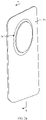
FIG. 2a is a schematic diagram of a rear cover of an electronic device according to an embodiment of the present application; -
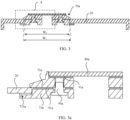
FIG. 3 is a schematic structural diagram showing cross sections of a camera decoration assembly and a rear cover in direction A-A inFIG. 2a ; -
FIG. 3a is an enlarged schematic structural diagram of part A inFIG. 3 ; -
FIG. 4 is a schematic structural diagram showing matching between a camera decoration assembly and a rear cover; -
FIG. 4a is an enlarged schematic structural diagram of part B inFIG. 4 ; -
FIG. 5 is a schematic diagram showing matching between a camera decoration assembly and a rear cover according to an embodiment of the present application; -
FIG. 5a is an enlarged schematic structural diagram of part C inFIG. 5 ; -
FIG. 5b is a schematic structural diagram showing part of matching between a camera decoration assembly and a rear cover according to an embodiment of the present application; -
FIG. 5c is a schematic diagram of disassembling the camera decoration assembly and the rear cover shown inFIG. 5 ; -
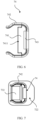
FIG. 6 is a schematic structural diagram of a connection assembly according to an embodiment of the present application; -
FIG. 7 is an internal view of a buckle cavity according to an embodiment of the present application; -
FIG. 8 is a schematic diagram of assembling a connection assembly and a second decoration part according to an embodiment of the present application; -
FIG. 9 is a schematic diagram showing matching between a connection assembly and a second decoration part according to an embodiment of the present application; -
FIG. 10 is a sectional view showing matching between a connection assembly and a second decoration part according to an embodiment of the present application; -
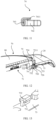
FIG. 11 is a sectional view of a connection assembly according to an embodiment of the present application; -
FIG. 12 is a schematic structural diagram showing part of matching between a camera decoration assembly and a rear cover according to an embodiment of the present application; and -
FIG. 13 is a schematic diagram of part of a structure of a second decoration part according to an embodiment of the present application. - Reference numerals in the accompanying drawings are as follows:
100: electronic device; 10: display screen; 20: rear cover; 21: opening; 30: middle frame; 31: metal middle plate; 32: rim; 40: circuit board; 50: battery; 60: camera module; 601: front-facing camera; 602: rear-facing camera; 70: camera decoration assembly; 71: photographing hole; 72: first decoration part; 721: first step; 7211: through hole; 722: buckle cavity; 7221: locking groove; 723: sealing cover; 724: convex edge; 725: mounting cavity; 726: second step; 727: hanging table; 73: second decoration part; 731: extension section; 732: buckle; 733: hanging table; 74: connection assembly; 741: locking structure; 7411: pin; 742: fixing structure; 743: reinforcing rib; 80: light-transmitting sheet; 90: connecting piece; and 91: binder. - Terms used in implementations of this application are used to only explain specific embodiments of this application, and are not intended to limit this application. The implementations of the embodiments of this application will be described in detail below with reference to the accompanying drawings.
- The embodiments of the present application provide an electronic device that may be, but is not limited to, a mobile phone, a tablet computer, a notebook computer, an ultra-mobile personal computer (Ultra-mobile Personal Computer, UMPC), a handheld computer, an intercom, a netbook, a POS terminal, a personal digital assistant (Personal Digital Assistant, PDA), a drive recorder, a security device, or another mobile or fixed terminal having a photographing function. The embodiments of the present application are described by using a mobile phone as an example.
-
FIG. 1 is a schematic structural diagram of an electronic device according to an embodiment of the present application.FIG. 2 is a schematic exploded structural diagram of an electronic device according to an embodiment of the present application. Referring toFIG. 1 andFIG. 2 , theelectronic device 100 provided in the embodiments of the present application may include a housing. The housing may provide a structural frame for theelectronic device 100. For example, inFIG. 2 , the housing may include amiddle frame 30 and arear cover 20. When theelectronic device 100 has a display function, theelectronic device 100 may be further provided with adisplay screen 10. Amiddle frame 30, acircuit board 40, and abattery 50 are disposed between thedisplay screen 10 and therear cover 20. Thecircuit board 40 and thebattery 50 may be disposed on themiddle frame 30. For example, thecircuit board 40 and thebattery 50 are disposed on a surface, facing therear cover 20, of themiddle frame 30; or thecircuit board 40 and thebattery 50 may be disposed on a surface, facing thedisplay screen 10, of themiddle frame 30. - It is easily understood that the housing of the electronic device provided in the present application includes, but is not limited to, the above structure. For example, in some other embodiments, the housing may be an integral or split housing made of metal, plastics, or the like. In the embodiments of the present application, the housing is specifically described by using a structure composed of the
middle frame 30 and therear cover 20 as an example. - The
battery 50 may be connected to thecircuit board 40, to supply power to a processor, an internal memory, an external memory, thedisplay screen 10, acamera module 60, a communications module, and the like. - The
display screen 10 may be an organic light-emitting diode (OLED), or a liquid crystal display (LCD). - The
rear cover 20 may be made of metal, glass, plastics, or ceramics. A material of therear cover 20 is not limited in the embodiments of the present application. - The
middle frame 30 may include amiddle plate 31 and arim 32. Therim 32 is provided around the outer periphery of themiddle plate 31. Generally, therim 32 may include a top frame, a bottom frame, a left side frame, and a right side frame. The top frame, the bottom frame, the left side frame, and the right side frame form a frame with a square ring structure. Themiddle plate 31 may be an aluminum plate, an aluminum alloy, or a magnesium alloy. Therim 32 may be made of metal or ceramics. The metalmiddle plate 31 and therim 32 may be clamped, welded, or bonded to each other, formed integrally, or fixedly connected via injection molding. - It should be noted that, in some other embodiments, the
electronic device 100 may include, but is not limited to, the structures shown inFIG. 1 andFIG. 2 . Therear cover 20 of the mobile phone may be connected to therim 32 to form an integral housing. For example, theelectronic device 100 may include thedisplay screen 10, the metalmiddle plate 31, and a shell. The shell may include therim 32 and therear cover 20 that are integrally formed. In this case, thecircuit board 40 and thebattery 50 are disposed in space enclosed by the metalmiddle plate 31 and the shell. - In the embodiments of the present application, the
electronic device 100 further includes at least onecamera module 60 and a flash (not shown in the figure), to implement the photographing function. Thecamera module 60 may be a front-facingcamera 601, a rear-facingcamera 602, or the like. There may be one or more front-facingcameras 601 or rear-facingcameras 602. For example, as shown inFIG. 2 , in theelectronic device 100 provided in the present application, thecamera module 60 includes a front-facingcamera 601 and a rear-facingcamera 602. In the embodiments of the present application, thecamera module 60 is described by using the rear-facingcamera 602 as an example. - The rear-facing
camera 602 and the flash may be disposed on a surface, facing therear cover 20, of the metalmiddle plate 31. Anopening 21, in which partial areas of the flash and the rear-facingcamera 602 can be mounted, is formed in therear cover 20. The front-facingcamera 601 may be disposed on a surface, facing thedisplay screen 10, of the metalmiddle plate 31. In the embodiments of the present application, disposing locations of the front-facingcamera 601 and the rear-facingcamera 602 include, but are not limited to, those in the above description. In some embodiments, there may be one or N front-facingcameras 601 and rear-facingcameras 602 in theelectronic device 100, and N is a positive integer greater than 1. - It may be understood that the schematic structure in this embodiment of this application constitutes no specific limitation on the
electronic device 100. In some other embodiments of this application, theelectronic device 100 may include more or fewer components than those shown in the figure, or some components may be combined, or some components may be split, or a different component deployment may be used. The components shown in the figure may be implemented by hardware, software, or a combination of software and hardware. - The
camera module 60 may include a lens, a filter, a support, a photosensitive element, a flexible plate, a connector, and the like. - It should be noted that, the
camera module 60 may have a focal length or a variable focal length. When thecamera module 60 has a variable focal length, thecamera module 60 may further include a focusing module (not shown in the figure), for example, a focusing motor. The focusing motor may be disposed on the support of the camera module. - In the embodiments of the present application, the filter may be disposed according to a functional requirement. For example, the filter may be an IR cut filter (IR cut Filter, IRCF). The IR cut filter can filter out infrared light, thereby avoiding an impact on imaging caused by infrared light entering the lens.
- The photosensitive element may be a charge coupled device (CCD) or a complementary metal-oxide-semiconductor (CMOS) phototransistor. The connector is configured to electrically connect the flexible plate with an image signal processor (Image Signal Processing, ISP) on the
circuit board 40. The image signal processor (ISP) is connected electrically to a digital signal processor (Digital Signal Processing, DSP). The image signal processor (ISP) and the digital signal processor (DSP) may be disposed on thecircuit board 40 independently or integrally. - During photographing, a shutter is enabled; light passes through the lens and is transmitted to the photosensitive element through the filter; a light signal is converted into an electrical signal; the photosensitive element transmits the electrical signal to the image signal processor (ISP) through the flexible plate and the connector; the image signal processor (ISP) converts the electrical signal into a digital image signal and outputs the digital image signal to the digital signal processor (DSP); and the digital signal processor (DSP) converts the digital image signal into an image signal in a standard format such as RGB or YUV.
-
FIG. 2a is a schematic diagram of a rear cover of an electronic device according to an embodiment of the present application. As shown inFIG. 2a , to guarantee aesthetics of the device and meet a mounting requirement, acamera decoration assembly 70 is generally disposed in theopening 21 in therear cover 20 when the rear-facingcamera 602 is disposed on therear cover 20 of theelectronic device 100. Thecamera decoration assembly 70 may be formed by splicing and assembling a plurality of components, such that thecamera decoration assembly 70 has diverse appearance effects, and flexibility in assembling thecamera decoration assembly 70 with therear cover 20 is increased. -
FIG. 3 is a schematic structural diagram showing cross sections of a camera decoration assembly and a rear cover in direction A-A inFIG. 2a .FIG. 3a is an enlarged schematic structural diagram of part A inFIG. 3 . Referring toFIG. 3a , thecamera decoration assembly 70a includes afirst decoration part 72a and asecond decoration part 73a. Thefirst decoration part 72a is disposed on an outer side of therear cover 20. An upper end surface of thefirst decoration part 72a is provided with a light-transmittingsheet 80a. Thesecond decoration part 73a is disposed below thefirst decoration part 72a. For example, as shown inFIG. 3a , a part of thesecond decoration part 73a is disposed in the opening 21 (referring toFIG. 2 ), and another part of thesecond decoration part 73a is disposed on an inner side of therear cover 20. Thesecond decoration part 73a is provided with a hanging table 733a. The hanging table 733a is in sealed connection with therear cover 20. Thefirst decoration part 72a and thesecond decoration part 73a are connected and sealed to each other through a connectingpiece 90a and abinder 91a. - It can be learned that because the
first decoration part 72a may be completely disposed on the outer side of therear cover 20, a size Wi of theopening 21 in therear cover 20 may be less than an outline dimension W2 (as shown inFIG. 3 ) of thecamera decoration assembly 70a. However, only an appearance surface of thefirst decoration part 72a is disposed on the outer side of the rear cover 20 (that is, thefirst decoration part 72a is exposed, but thesecond decoration part 73a is not exposed); and generally, thefirst decoration part 72a is made of a single material or has a single color. This limits appearance diversity of thecamera decoration assembly 70a, and goes against diverse design for decorating a camera on therear cover 20. In addition, thefirst decoration part 72a and thesecond decoration part 73a are connected to each other through a screw (namely, the connectingpiece 90a). However, the screw can be generally arranged only in a thick enough area of thecamera decoration assembly 70a, but is hard to be arranged in a relatively thin area of thecamera decoration assembly 70a (for example, areas, near therear cover 20, of thefirst decoration part 72a and thesecond decoration part 73a). As a result, stability of combination between thecamera decoration assembly 70a and therear cover 20 is weak, causing looseness of thecamera decoration assembly 70a. -
FIG. 4 is a schematic structural diagram showing matching between a camera decoration assembly and a rear cover.FIG. 4a is an enlarged schematic structural diagram of part B inFIG. 4 . Referring toFIG. 4a , thecamera decoration assembly 70b includes afirst decoration part 72b and asecond decoration part 73b. An upper end surface of thefirst decoration part 72b is provided with light-transmittingsheet 80b. Thefirst decoration part 72b is provided with a hanging table 727b. Thesecond decoration part 73b is provided with a hanging table 733b. An upper surface and a lower surface of the hanging table 727b are respectively in sealed connection with an inner surface of therear cover 20 and an upper surface of the hanging table 733b through abinder 91b. Thefirst decoration part 72b sleeves thesecond decoration part 73b. From the perspective of a visual effect, both thefirst decoration part 72b and thesecond decoration part 73b are exposed. Thefirst decoration part 72b and thesecond decoration part 73b may be made of different materials, and have different colors, patterns, and the like, thereby achieving different appearance effects. - However, referring to
FIG. 4 , a size W3 of theopening 21 in therear cover 20 needs to be greater than an outline dimension W4 of thecamera decoration assembly 70b. In this case, strength of therear cover 20 is weaken accordingly. In addition, connection among thefirst decoration part 72b, thesecond decoration part 73b, and therear cover 20 is implemented in a manner of laminating and bonding therear cover 20, the hanging table 727b, and the hanging table 733b. This manner still imposes a relatively high requirement for internal space of therear cover 20, which limits minimization and thinning of an overall dimension of theelectronic device 100. - To resolve the above problems,
FIG. 5 is a schematic diagram showing matching between a camera decoration assembly and a rear cover according to an embodiment of the present application;FIG. 5a is an enlarged schematic structural diagram of part C inFIG. 5 ; andFIG. 5b is a schematic structural diagram showing part of matching between a camera decoration assembly and a rear cover according to an embodiment of the present application. Referring toFIG. 5 andFIG. 5a , in the embodiments of the present application, theelectronic device 100 further includes acamera decoration assembly 70. Thecamera decoration assembly 70 penetrates the opening 21 (referring toFIG. 2 ) formed in therear cover 20. - The
camera decoration assembly 70 is provided with a photographinghole 71 allowing thecamera module 60 to perform photographing. Thecamera module 60 is disposed near thecamera decoration assembly 70. For example, the lens of thecamera module 60 is fixedly or telescopically disposed in the photographinghole 71; or the lens of thecamera module 60 is disposed in therear cover 20 of theelectronic device 100 and does not extend into the photographinghole 71 when the lens is in a standby state, and can extend into the photographinghole 71 when the lens is in a working state. - Still referring to
FIG. 5a andFIG. 5b , Thecamera decoration assembly 70 may include afirst decoration part 72, asecond decoration part 73, and at least oneconnection assembly 74 configured to connect thefirst decoration part 72 to thesecond decoration part 73. - During assembly, a first end of the
first decoration part 72 penetrates the opening 21 (referring toFIG. 2 and a range denoted by W5 inFIG. 5 ) and is disposed outside therear cover 20. A second end of thefirst decoration part 72 is disposed in therear cover 20 and is in sealed connection with the inner surface of therear cover 20. - For example, in
FIG. 5a , therear cover 20 is used for reference. An upper part of therear cover 20 is defined as an exterior of therear cover 20; and a lower part of therear cover 20 is defined as an interior of therear cover 20. - The
second decoration part 73 sleeves an outer side surface at an end, outside therear cover 20, of thefirst decoration part 72; and an outer edge of thesecond decoration part 73 extends to an outer surface of therear cover 20. When there are a plurality ofconnection assemblies 74, the connection assemblies 74 (for example, four connection assemblies or five connection assemblies) may be disposed at a periphery of thefirst decoration part 72, thereby enhancing connection between thesecond decoration part 73 and thefirst decoration part 72. In addition, thefirst decoration part 72 and thesecond decoration part 73 may be made of different materials, and have different colors, glyphs, patterns, and the like, thereby enriching an appearance effect of thecamera decoration assembly 70, and increasing overall aesthetics of the electronic device. Certainly, in some examples, thefirst decoration part 72 and thesecond decoration part 73 may have a same color and a same pattern. - It should be understood that when the
second decoration part 73 sleeves thefirst decoration part 72, and the outer edge of thesecond decoration part 73 may extend to the outer surface of therear cover 20, such that the outline dimension W5 of theopening 21 formed in therear cover 20 can be less than an outline dimension W6 (as shown inFIG. 5 ) of thecamera decoration assembly 70, thereby enhancing overall strength of therear cover 20. In addition, when the outer edge of thesecond decoration part 73 extends to the outer surface of therear cover 20, an assembling junction between thecamera decoration assembly 70 and theopening 21 in therear cover 20 can be hidden, thereby avoiding an impact on an appearance of therear cover 20 caused by exposure of assembling locations, in theopening 21, of therear cover 20 and thecamera decoration assembly 70. A gap between thecamera decoration assembly 70 and therear cover 20 is hidden in appearance, for example, a gap, outside the housing, betweenfirst decoration part 72b and therear cover 20 inFIG. 4a , thereby preventing accumulation of dust and increasing overall exquisiteness of the electronic device. - In addition, the
camera decoration assembly 70 provided in the present application has a simple structure, occupies less space, and is more flexible to disassemble. - It should be noted that, in some embodiments of the present application, the
second decoration part 73 may be disassembled into a plurality of circular decoration parts. The circular decoration parts sequentially sleeve an outer side surface at an end, outside therear cover 20, of thefirst decoration part 72 in circles one by one. In addition, an outer edge of a circular decoration part in the outermost circle extends to the outer surface of therear cover 20. - In some embodiments of the present application, a top surface of the
second decoration part 73, namely, a surface, facing the exterior of therear cover 20, of thesecond decoration part 73 may be an inclined surface (as shown inFIG. 5a ) inclined to therear cover 20. In this way, the appearance effect of thecamera decoration assembly 70 can be enriched; user's touch feeling can be enhanced; and user's experience effect can be improved. - Certainly, in some embodiments of the present application, the top surface of the
second decoration part 73 may be a plane (as shown inFIG. 5b ) extending towards therear cover 20, that is, a surface, away from the interior of therear cover 20, of thesecond decoration part 73 is parallel to the outer surface of therear cover 20. A shape of the top surface of thesecond decoration part 73 is not limited herein. - Still referring to
FIG. 5a , in some embodiments of the present application, an outer surface, between the first end outside therear cover 20 and the second end inside therear cover 20, of thefirst decoration part 72 may be provided with afirst step 721, to facilitate disassembly of thecamera decoration assembly 70, improve flexibility in disassembling thecamera decoration assembly 70, and increase structural stability of thecamera decoration assembly 70. Thefirst step 721 is disposed in theopening 21 and configured to support part of thesecond decoration part 73. The part of thesecond decoration part 73 is disposed on and connected to thefirst step 721, thereby guaranteeing stability of the second decoration part 7. - The part of the
second decoration part 73 is connected to thefirst step 721 through at least oneconnection assembly 74. For example, in some embodiments of the present application, theconnection assembly 74 is a screw (not shown in the figure). A throughhole 7211 may be formed in thefirst step 721. A threaded hole (not shown in the figure) may be formed, corresponding to the throughhole 7211, in thesecond decoration part 73. During assembly, the screw penetrates the throughhole 7211 from the interior of therear cover 20 and is connected to the threaded hole, thereby implementing connection between thefirst decoration part 72 and thesecond decoration part 73. - For another example, in some embodiments of the present application, referring to
FIG. 5a , a surface, facing thefirst step 721, of thesecond decoration part 73 is provided with anextension section 731. An end of theextension section 731 is provided with abuckle 732. A throughhole 7211 allowing theextension section 731 and thebuckle 732 to penetrate is formed in thefirst step 721. Connection between thefirst decoration part 72 and thesecond decoration part 73 is implemented via locking between theconnection assembly 74 and thebuckle 732. - A
binder 91 may be disposed between a hole wall of the throughhole 7211 and theextension section 731, thereby implementing a function of preventing water and dust. - Referring to
FIG. 5a , in some embodiments of the present application, a surface (namely, a bottom surface of the first decoration part 72), facing the interior of therear cover 20, of thefirst decoration part 72 may be further provided with abuckle cavity 722, to prevent components such as thebuckle 732 and theconnection assembly 74 from interfering with an internal structure of theelectronic device 100. Thebuckle cavity 722 may be an accommodation cavity formed in an end surface, inside therear cover 20, of thefirst decoration part 72. In addition, thebuckle cavity 722 is communicated with the throughhole 7211. Thebuckle cavity 722 may encircle the components such as thebuckle 732 and theconnection assembly 74. In this case, alocking groove 7221 used for locking apin 7411 of theconnection assembly 74 is formed in a gap between thebuckle 732 and an inner wall of thebuckle cavity 722. Thepin 7411 can be inserted into the lockinggroove 7221. Owing to thebuckle cavity 722, theconnection assembly 74 and thebuckle 732 do not occupy internal space of the electronic device. Therefore, theconnection assembly 74 and thebuckle 732 do not interfere with an internal device of the electronic device. - Referring to
FIG. 5a , in a possible implementation of the present application, theelectronic device 100 may further include a sealingcover 723. The sealingcover 723 covers and seals an opening, facing the interior of therear cover 20, of thebuckle cavity 722, thereby preventing liquid and dust from entering theelectronic device 100 through the throughhole 7211, and implementing the function of preventing dust and water. - When the
electronic device 100 has a higher requirement for dust prevention and water prevention, thebuckle cavity 722 may be further filled with a sealing glue. In addition, filling with the sealing glue can also reinforce a structure of thecamera decoration assembly 70. - As a manner of sealed connection between the
first decoration part 72 and therear cover 20, asecond step 726 may be disposed at the second end of thefirst decoration part 72, namely, the end in therear cover 20. A surface, facing the first end of thefirst decoration part 72, of thesecond step 726 is in sealed connection with the inner surface of therear cover 20. As shown inFIG. 5a , an upper surface of thesecond step 726 is in sealed connection with a lower surface of therear cover 20. A manner of the sealed connection may be using a binder to bond the second step with therear cover 20, thereby guaranteeing dust-proof and water-proof performance. - It is easily understood that when the
camera decoration assembly 70 is in sealed connection with therear cover 20 in the above manner, a dimension, inside therear cover 20, of thecamera decoration assembly 70 is a thickness of thesecond step 726, such that thecamera decoration assembly 70 occupies less internal space of therear cover 20. Therefore, theelectronic device 100 can develop in a minimizing and thinning trend. Moreover, thecamera decoration assembly 70 includes afirst decoration part 72 and asecond decoration part 73. Thefirst decoration part 72 may adopt a built-in scheme shown inFIG. 5a , and may be connected to an inner side surface of therear cover 20 from the interior of therear cover 20 through thesecond step 726. Thesecond decoration part 73 may adopt a built-out scheme shown inFIG. 5c , and may be connected to thefirst decoration part 72 after penetrating the throughhole 7211 from the exterior of therear cover 20, such that a width (for example, a range denoted by W7 inFIG. 5a ) of a matching surface between thefirst decoration part 72 and thesecond decoration part 73 in limited mounting space is small. When thefirst decoration part 72 and thesecond decoration part 73 respectively adopt the built-in scheme and the built-out scheme, an area of an assembling and matching surface between thesecond decoration part 73 and thefirst step 721 of thefirst decoration part 72 can be relatively small, which facilitates minimization of theopening 21 to enhance the overall strength of therear cover 20. - In addition, the
binder 91 may be further disposed between thesecond decoration part 73 and an outer side surface at an end, outside therear cover 20, of thefirst decoration part 72, between thesecond decoration part 73 and thesecond step 726, and between the throughhole 7211 and theextension section 731, to enhance tightness of thecamera decoration assembly 70 while further guaranteeing dust-proof and water-proof performance of thecamera decoration assembly 70. - Still referring to
FIG. 5a , in this embodiment of the present application, theelectronic device 100 may further include a light-transmittingsheet 80. The light-transmittingsheet 80 is disposed on a top surface of thefirst decoration part 72, namely, an end surface, facing the exterior of therear cover 20, of thefirst decoration part 72. Referring toFIG. 5c , a periphery on the top surface of thefirst decoration part 72 may be provided with aconvex edge 724, to enhance assembling stability of the light-transmittingsheet 80. Theconvex edge 724 and the top surface of thefirst decoration part 72 define a mountingcavity 725. The light-transmittingsheet 80 is disposed in the mountingcavity 725, and can be in sealed connection with the top surface of thefirst decoration part 72 by using thebinder 91. -
FIG. 6 is a schematic structural diagram of a connection assembly according to an embodiment of the present application. Referring toFIG. 5a andFIG. 6 , theconnection assembly 74 may include a lockingstructure 741. An outer diameter of the lockingstructure 741 is greater than an aperture of the throughhole 7211. An end of the lockingstructure 741 is provided with apin 7411. Thepin 7411 is configured to be locked to thebuckle 732. Specifically, referring toFIG. 5a , when thebuckle 732 penetrates the throughhole 7211, there is a certain gap between thebuckle 732 and a lower surface of thefirst step 721. When thepin 7411 is inserted into the gap, stability of thesecond decoration part 73 is guaranteed to prevent thesecond decoration part 73 from getting loose, and theextension section 731 is prevented from being pulled out of the throughhole 7211. Therefore, tightness of thesecond decoration part 73 is guaranteed. - Still referring to
FIG. 6 , in some embodiments of the present application, theconnection assembly 74 may further include fixingstructures 742. The fixingstructures 742 are configured to clamp theconnection assembly 74 on thebuckle 732, thereby guaranteeing stability of thesecond decoration part 73. For example, as shown inFIG. 6 , the fixingstructures 742 are respectively disposed at two ends of the lockingstructure 741, thereby forming a hooping structure. Referring toFIG. 7 to FIG. 10 ,FIG. 7 is an internal view of a buckle cavity according to an embodiment of the present application;FIG. 8 is a schematic diagram of assembling a connection assembly and a second decoration part according to an embodiment of the present application;FIG. 9 is a schematic diagram showing matching between a connection assembly and a second decoration part according to an embodiment of the present application; andFIG. 10 is a sectional view showing matching between a connection assembly and a second decoration part according to an embodiment of the present application. The fixingstructures 742 hoop thebuckle 732, such that theconnection assembly 74 is clamped on thebuckle 732, and theconnection assembly 74 and thebuckle 732 are prevented from getting loose. -
FIG. 11 is a sectional view of a connection assembly according to an embodiment of the present application. Referring toFIG. 11 , theconnection assembly 74 may be further provided with a reinforcingrib 743, to reinforce a structure of theconnection assembly 74. -
FIG. 12 is a schematic structural diagram showing part of matching between a camera decoration assembly and a rear cover according to an embodiment of the present application. Referring toFIG. 12 , in this embodiment of the present application, theelectronic device 100 further includes acamera decoration assembly 70. Thecamera decoration assembly 70 penetrates the opening 21 (referring toFIG. 2 ) formed in therear cover 20. - The
camera decoration assembly 70 is provided with a photographinghole 71 allowing thecamera module 60 to perform photographing. Thecamera module 60 is disposed near thecamera decoration assembly 70. For example, the lens of thecamera module 60 is fixedly or telescopically disposed in the photographinghole 71; or the lens of thecamera module 60 is disposed in therear cover 20 of theelectronic device 100 and does not extend into the photographinghole 71 when the lens is in a standby state, and can extend into the photographinghole 71 when the lens is in a working state. - Still referring to
FIG. 12 , thecamera decoration assembly 70 may include afirst decoration part 72, asecond decoration part 73, and at least oneconnection assembly 74 configured to connect thefirst decoration part 72 to thesecond decoration part 73. - During assembly, a first end of the
first decoration part 72 penetrates the opening 21 (referring toFIG. 2 and a range denoted by W5 inFIG. 5 ) and is disposed outside therear cover 20. A second end of thefirst decoration part 72 is disposed in therear cover 20 and is in sealed connection with the inner surface of therear cover 20. - For example, in
FIG. 12 , therear cover 20 is used for reference. An upper part of therear cover 20 is defined as an exterior of therear cover 20; and a lower part of therear cover 20 is defined as an interior of therear cover 20. - The
second decoration part 73 sleeves an outer side surface at an end, outside therear cover 20, of thefirst decoration part 72; and an outer edge of thesecond decoration part 73 extends to an outer surface of therear cover 20. When there are a plurality ofconnection assemblies 74, the connection assemblies 74 (for example, four connection assemblies or five connection assemblies) may be disposed at a periphery of thefirst decoration part 72, thereby enhancing connection between thesecond decoration part 73 and thefirst decoration part 72. In addition, thefirst decoration part 72 and thesecond decoration part 73 may be made of different materials, and have different colors, glyphs, patterns, and the like, thereby enriching an appearance effect of thecamera decoration assembly 70, and increasing overall aesthetics of the electronic device. Certainly, in some examples, thefirst decoration part 72 and thesecond decoration part 73 may have a same color and a same pattern. - It should be understood that when the
second decoration part 73 sleeves thefirst decoration part 72, and the outer edge of thesecond decoration part 73 may extend to the outer surface of therear cover 20, such that the outline dimension of theopening 21 formed in therear cover 20 can be less than the outline dimension (for a principle, refer toFIG. 5 of embodiment 1) of thecamera decoration assembly 70, thereby enhancing overall strength of therear cover 20. In addition, when the outer edge of thesecond decoration part 73 extends to the outer surface of therear cover 20, an assembling junction between thecamera decoration assembly 70 and theopening 21 in therear cover 20 can be hidden, thereby avoiding an impact on an appearance of therear cover 20 caused by exposure of assembling locations, in theopening 21, of therear cover 20 and thecamera decoration assembly 70. A gap between thecamera decoration assembly 70 and therear cover 20 is hidden in appearance, for example, a gap, outside the housing, betweenfirst decoration part 72b and therear cover 20 inFIG. 4a , thereby preventing accumulation of dust and increasing overall exquisiteness of the electronic device. - In addition, the
camera decoration assembly 70 provided in the present application has a simple structure, occupies less space, and is more flexible to disassemble. - It should be noted that, in some embodiments of the present application, the
second decoration part 73 may be disassembled into a plurality of circular decoration parts. The circular decoration parts sequentially sleeve an outer side surface at an end, outside therear cover 20, of thefirst decoration part 72 in circles one by one. In addition, an outer edge of a circular decoration part in the outermost circle extends to the outer surface of therear cover 20. - In some embodiments of the present application, a top surface of the
second decoration part 73, namely, a surface, facing the exterior of therear cover 20, of thesecond decoration part 73 may be a plane (as shown inFIG. 12 ) extending towards therear cover 20. Certainly, the surface may alternatively be an inclined surface inclined to therear cover 20. In this way, the appearance effect of thecamera decoration assembly 70 can be enriched; user's touch feeling can be enhanced; and user's experience effect can be improved. - Still referring to
FIG. 12 , in some embodiments of the present application, an outer surface, between the first end outside therear cover 20 and the second end inside therear cover 20, of thefirst decoration part 72 may be provided with afirst step 721, to facilitate disassembly of thecamera decoration assembly 70, improve flexibility in disassembling thecamera decoration assembly 70, and increase structural stability of thecamera decoration assembly 70. Thefirst step 721 is disposed in theopening 21 and configured to support part of thesecond decoration part 73. The part of thesecond decoration part 73 is disposed on and connected to thefirst step 721, thereby guaranteeing stability of the second decoration part 7. - In some embodiments of the present application, a surface, facing the
first step 721, of thesecond decoration part 73 is provided with anextension section 731. An end of theextension section 731 is provided with abuckle 732. A throughhole 7211 allowing theextension section 731 and thebuckle 732 to penetrate is formed in thefirst step 721. - An end surface, inside the
rear cover 20, of thefirst decoration part 72 is provided with abuckle cavity 722. Thebuckle cavity 722 is communicated with the throughhole 7211. Thebuckle 732 is disposed in thebuckle cavity 722. Theconnection assembly 74 is configured to connect to at least thebuckle 732, thereby connecting thesecond decoration part 73 to thefirst decoration part 72. - The
connection assembly 74 may include a sealing glue, which may be understood as that thebuckle cavity 722 is filled with the sealing glue, thereby fixing the buckle in thebuckle cavity 722. In addition, assembling between thefirst decoration part 72 andsecond decoration part 73 may be fixed by dispensing the glue. After the dispensing is completed, curing is performed within specified time. -
FIG. 13 is a schematic diagram of part of a structure of a second decoration part according to an embodiment of the present application. Referring toFIG. 13 , in some embodiments of the present application, thebuckle 732 may be T-shaped. In this case, drawing force on thesecond decoration part 73 after the sealing glue is cured can be increased. Certainly, thebuckle 732 may alternatively be L-shaped as in embodiment 1, or umbrella-shaped. A shape of thebuckle 732 is not limited herein. - Certainly, the
electronic device 100 may further include a sealing cover. The sealing cover covers and seals an opening, facing the interior of therear cover 20, of thebuckle cavity 722, thereby preventing liquid and dust from entering theelectronic device 100 through the through hole, and implementing a function of preventing dust and water. - As a manner of sealed connection between the
first decoration part 72 and therear cover 20, asecond step 726 may be disposed at the second end of thefirst decoration part 72, namely, the end in therear cover 20. A surface, facing the first end of thefirst decoration part 72, of thesecond step 726 is in sealed connection with the inner surface of therear cover 20. As shown inFIG. 12 , an upper surface of thesecond step 726 is in sealed connection with a lower surface of therear cover 20. A manner of the sealed connection may be using a binder to bond the second step with therear cover 20, thereby guaranteeing dust-proof and water-proof performance. - It is easily understood that when the
camera decoration assembly 70 is in sealed connection with therear cover 20 in the above manner, a dimension, inside therear cover 20, of thecamera decoration assembly 70 is a thickness of thesecond step 726, such that thecamera decoration assembly 70 occupies less internal space of therear cover 20. Therefore, theelectronic device 100 can develop in a minimizing and thinning trend. Moreover, thecamera decoration assembly 70 includes afirst decoration part 72 and asecond decoration part 73. Thefirst decoration part 72 may adopt a built-in scheme shown inFIG. 5a , and may be connected to an inner side surface of therear cover 20 from the interior of therear cover 20 through thesecond step 726. Thesecond decoration part 73 may adopt a built-out scheme shown inFIG. 5c , and may be connected to thefirst decoration part 72 after penetrating the throughhole 7211 from the exterior of therear cover 20, such that a width (for example, a range denoted by W7 inFIG. 5a ) of a matching surface between thefirst decoration part 72 and thesecond decoration part 73 in limited mounting space is small. When thefirst decoration part 72 and thesecond decoration part 73 respectively adopt the built-in scheme and the built-out scheme, an area of an assembling and matching surface between thesecond decoration part 73 and thefirst step 721 of thefirst decoration part 72 can be relatively small, which facilitates minimization of theopening 21 to enhance the overall strength of therear cover 20. - In addition, the binder may be further disposed between the
second decoration part 73 and an outer side surface at an end, outside therear cover 20, of thefirst decoration part 72, between a hole wall of the throughhole 7211 and theextension section 731, between thesecond decoration part 73 and thesecond step 726, and between the throughhole 7211 and theextension section 731, to enhance tightness of thecamera decoration assembly 70 while further guaranteeing dust-proof and water-proof performance of thecamera decoration assembly 70. - Still referring to
FIG. 12 , in this embodiment of the present application, theelectronic device 100 may further include a light-transmittingsheet 80. The light-transmittingsheet 80 is disposed on a top surface of thefirst decoration part 72, namely, an end surface, facing the exterior of therear cover 20, of thefirst decoration part 72. A periphery on the top surface of thefirst decoration part 72 may be provided with aconvex edge 724, to enhance assembling stability of the light-transmittingsheet 80. Theconvex edge 724 and the top surface of thefirst decoration part 72 define a mounting cavity. The light-transmittingsheet 80 is disposed in the mounting cavity, and can be in sealed connection with the top surface of thefirst decoration part 72 by using the binder. - In conclusion, the
electronic device 100 provided in the embodiments of the present application has the following advantage: The size of theopening 21 in therear cover 20 can be decreased while thecamera decoration assembly 70 has diverse appearance effects, thereby guaranteeing overall strength of therear cover 20. Moreover, a form of connection between thebuckle 732 and theconnection assembly 74 facilitates disassembly, decreases occupied space, and can increase flexibility in disassembling thecamera decoration assembly 70. Thecamera decoration assembly 70 may also be disassembled from the perspective of appearance. In addition, an overall structure of thecamera decoration assembly 70 is simple, such that the camera decoration assembly occupies less internal space of theelectronic device 100. This can further minimize and thin theelectronic device 100. Moreover, a gap between thecamera decoration assembly 70 and therear cover 20 can be hidden in appearance, thereby preventing accumulation of dust and increasing overall exquisiteness of the electronic device. In theelectronic device 100 provided in the embodiments of the present application, structural stability and reliability of thecamera decoration assembly 70 can also be enhanced. - In the descriptions of the embodiments of this application, it is to be noted that, unless otherwise specified or defined, the terms such as "mount", "connect", and "connection" should be understood in a broad sense, for example, which may be a fixed connection, an indirect connection through an intermediary, or internal communication between two components or mutual interaction relationship between two components. A person of ordinary skill in the art may understand the specific meanings of the foregoing terms in the embodiments of this application according to specific situations.
- In the specification, claims, and accompanying drawings of the embodiments of this application, the terms "first", "second", "third", "fourth", and so on (if existent) are intended to distinguish between similar objects but do not necessarily indicate a specific order or sequence.
- Finally, it is to be noted that the foregoing embodiments are merely intended for describing the technical solutions of this application, but are not intended to limit this application. Although this application is described in detail with reference to the foregoing embodiments, it should be appreciated by a person of ordinary skill in the art that, modifications may still be made to the technical solutions recorded in the foregoing embodiments, or equivalent replacements may be made to the part of all of the technical features; and these modifications or replacements will not cause the essence of corresponding technical solutions to depart from the scope of the technical solutions in the embodiments of this application.
Claims (32)
- An electronic device, at least comprising: a housing and at least one camera module, wherein an opening is formed in the housing;the electronic device further comprises a camera decoration assembly, wherein the camera decoration assembly penetrates the opening, and the camera module is disposed near the camera decoration assembly;the camera decoration assembly comprises a first decoration part, a second decoration part, and at least one connection assembly configured to connect the first decoration part to the second decoration part;a first end of the first decoration part penetrates the opening and is disposed outside the housing, and a second end of the first decoration part is disposed in the housing and connected to an inner surface of the housing; andthe second decoration part sleeves an outer side surface, outside the housing, of the first decoration part, and an outer edge of the second decoration part extends to an outer surface of the housing.
- The electronic device according to claim 1, wherein an outer surface between the first end and the second end of the first decoration part is provided with a first step, the first step is disposed in the opening, and the second decoration part is partially disposed on and connected to the first step.
- The electronic device according to claim 2, wherein a surface, facing the first step, of the second decoration part is provided with an extension section, an end of the extension section is provided with a buckle, and a through hole allowing the extension section and the buckle to penetrate is formed in the first step; and
the connection assembly is configured to connect to at least the buckle, thereby connecting the second decoration part to the first decoration part. - The electronic device according to claim 3, wherein an end surface, in the housing, of the first decoration part is provided with a buckle cavity, the buckle cavity is communicated with the through hole, and the buckle is disposed in the buckle cavity.
- The electronic device according to claim 4, wherein the connection assembly comprises a sealing glue; and
the buckle cavity is filled with the sealing glue, and the sealing glue is used to fix the buckle in the buckle cavity. - The electronic device according to claim 4 or 5, wherein the connection assembly comprises a locking structure, an end of the locking structure is provided with a pin, a locking groove is formed between the buckle and an inner wall of the buckle cavity, and the pin is disposed in the locking groove.
- The electronic device according to claim 6, wherein the connection assembly further comprises fixing structures, and the fixing structures are respectively disposed at two ends of the locking structure and are used to clamp the buckle.
- The electronic device according to any one of claims 4 to 7, further comprising: a sealing cover, wherein the sealing cover covers and seals an opening, facing an interior of the housing, of the buckle cavity.
- The electronic device according to any one of claims 6 to 8, wherein the connection assembly is provided with a reinforcing rib.
- The electronic device according to any one of claims 1 to 9, wherein the second end of the first decoration part is provided with a second step, and a surface, facing the first end of the first decoration part, of the second step is in sealed connection with the housing.
- The electronic device according to any one of claims 2 to 9, wherein a binder is disposed between the second decoration part and the first step; and
the binder is also disposed between the second decoration part and an outer side surface at an end, outside the housing, of the first decoration part. - The electronic device according to any one of claims 1 to 11, further comprising: a light-transmitting sheet, wherein
the light-transmitting sheet is disposed on a top surface of the first decoration part. - The electronic device according to claim 12, wherein a periphery of the top surface of the first decoration part is provided with a convex edge, the convex edge and the top surface of the first decoration part define a mounting cavity, and the mounting cavity is used for mounting of the light-transmitting sheet.
- The electronic device according to any one of claims 1 to 13, wherein a surface, away from an interior of the housing, of the second decoration part is an inclined surface inclined to the housing.
- The electronic device according to any one of claims 1 to 13, wherein a surface, away from an interior of the housing, of the second decoration part is parallel to the outer surface of the housing.
- The electronic device according to claim 2, wherein the connection assembly comprises a screw; and
the second decoration part is provided with a threaded hole, a through hole is formed in the first step, and the screw penetrates the through hole and is connected to the threaded hole. - An electronic device, at least comprising: a housing and at least one camera module, wherein an opening is formed in the housing;the electronic device further comprises a camera decoration assembly, wherein the camera decoration assembly penetrates the opening, and the camera module is disposed near the camera decoration assembly;the camera decoration assembly comprises a first decoration part, a second decoration part, and at least one connection assembly configured to connect the first decoration part to the second decoration part;a first end of the first decoration part penetrates the opening and is disposed outside the housing, and a second end of the first decoration part is disposed in the housing and connected to an inner surface of the housing;the second decoration part sleeves an outer side surface, outside the housing, of the first decoration part, and an outer edge of the second decoration part extends to an outer surface of the housing;an outer surface between the first end and the second end of the first decoration part is provided with a first step, the first step is disposed in the opening, and the second decoration part is partially disposed on and connected to the first step;a surface, facing the first step, of the second decoration part is provided with an extension section, an end of the extension section is provided with a buckle, and a through hole allowing the extension section and the buckle to penetrate is formed in the first step; andthe connection assembly is configured to connect to at least the buckle, thereby connecting the second decoration part to the first decoration part.
- The electronic device according to claim 17, wherein an end surface, in the housing, of the first decoration part is provided with a buckle cavity, the buckle cavity is communicated with the through hole, and the buckle is disposed in the buckle cavity.
- The electronic device according to claim 18, wherein the connection assembly comprises a sealing glue; and
the buckle cavity is filled with the sealing glue, and the sealing glue is used to fix the buckle in the buckle cavity. - The electronic device according to claim 18, wherein the connection assembly comprises a locking structure, an end of the locking structure is provided with a pin, a locking groove is formed between the buckle and an inner wall of the buckle cavity, and the pin is disposed in the locking groove.
- The electronic device according to claim 19, wherein the connection assembly comprises a locking structure, an end of the locking structure is provided with a pin, a locking groove is formed between the buckle and an inner wall of the buckle cavity, and the pin is disposed in the locking groove.
- The electronic device according to claim 20, wherein the connection assembly further comprises fixing structures, and the fixing structures are respectively disposed at two ends of the locking structure and are used to clamp the buckle.
- The electronic device according to claim 21, wherein the connection assembly further comprises fixing structures, and the fixing structures are respectively disposed at two ends of the locking structure and are used to clamp the buckle.
- The electronic device according to any one of claims 18 to 23, further comprising: a sealing cover, wherein the sealing cover covers and seals an opening, facing an interior of the housing, of the buckle cavity.
- The electronic device according to any one of claims 20 to 23, wherein the connection assembly is provided with a reinforcing rib.
- The electronic device according to any one of claims 17 to 23, wherein the second end of the first decoration part is provided with a second step, and a surface, facing the first end of the first decoration part, of the second step is in sealed connection with the housing.
- The electronic device according to any one of claims 17 to 23, wherein a binder is disposed between the second decoration part and the first step; and
the binder is also disposed between the second decoration part and an outer side surface at an end, outside the housing, of the first decoration part. - The electronic device according to any one of claims 17 to 23, further comprising: a light-transmitting sheet, wherein
the light-transmitting sheet is disposed on a top surface of the first decoration part. - The electronic device according to claim 28, wherein a periphery of the top surface of the first decoration part is provided with a convex edge, the convex edge and the top surface of the first decoration part define a mounting cavity, and the mounting cavity is used for mounting of the light-transmitting sheet.
- The electronic device according to any one of claims 17 to 23, wherein a surface, away from an interior of the housing, of the second decoration part is an inclined surface inclined to the housing.
- The electronic device according to any one of claims 17 to 23, wherein a surface, away from an interior of the housing, of the second decoration part is parallel to the outer surface of the housing.
- The electronic device according to claim 17, wherein the connection assembly comprises a screw; and
the second decoration part is provided with a threaded hole, a through hole is formed in the first step, and the screw penetrates the through hole and is connected to the threaded hole.
Applications Claiming Priority (2)
| Application Number | Priority Date | Filing Date | Title |
|---|---|---|---|
| CN202110753742.1A CN113726926B (en) | 2021-07-02 | 2021-07-02 | Electronic device |
| PCT/CN2022/093682 WO2023273677A1 (en) | 2021-07-02 | 2022-05-18 | Electronic device |
Publications (3)
| Publication Number | Publication Date |
|---|---|
| EP4138372A1 true EP4138372A1 (en) | 2023-02-22 |
| EP4138372A4 EP4138372A4 (en) | 2023-11-08 |
| EP4138372B1 EP4138372B1 (en) | 2024-09-18 |
Family
ID=78673042
Family Applications (1)
| Application Number | Title | Priority Date | Filing Date |
|---|---|---|---|
| EP22777211.8A Active EP4138372B1 (en) | 2021-07-02 | 2022-05-18 | Electronic device |
Country Status (4)
| Country | Link |
|---|---|
| US (1) | US12348658B2 (en) |
| EP (1) | EP4138372B1 (en) |
| CN (1) | CN113726926B (en) |
| WO (1) | WO2023273677A1 (en) |
Families Citing this family (9)
| Publication number | Priority date | Publication date | Assignee | Title |
|---|---|---|---|---|
| CN113726926B (en) | 2021-07-02 | 2022-06-24 | 荣耀终端有限公司 | Electronic device |
| CN218276765U (en) * | 2022-01-26 | 2023-01-10 | 荣耀终端有限公司 | an electronic device |
| CN114172989B (en) * | 2022-02-11 | 2022-06-17 | 荣耀终端有限公司 | Electronic device and method for assembling electronic device |
| CN114979450B (en) * | 2022-07-22 | 2022-12-23 | 荣耀终端有限公司 | A camera decorative bracket, a camera decorative component and electronic equipment |
| KR20240066220A (en) * | 2022-11-04 | 2024-05-14 | 삼성전자주식회사 | Electronic device including camera |
| CN115604556B (en) * | 2022-12-01 | 2023-09-05 | 荣耀终端有限公司 | Camera decoration assembly and electronic equipment |
| CN116193013B (en) * | 2023-04-24 | 2024-04-16 | 荣耀终端有限公司 | Electronic equipment |
| CN117295270B (en) * | 2023-09-25 | 2025-01-03 | 荣耀终端有限公司 | Decoration, housing assembly and electronic equipment |
| CN121125892A (en) * | 2024-06-05 | 2025-12-12 | 荣耀终端股份有限公司 | Screen components and electronic devices |
Family Cites Families (14)
| Publication number | Priority date | Publication date | Assignee | Title |
|---|---|---|---|---|
| US9395602B2 (en) * | 2014-01-15 | 2016-07-19 | Apple Inc. | Suspension for camera trim enabling thinner camera stack |
| CN107493358A (en) * | 2017-08-07 | 2017-12-19 | 广东欧珀移动通信有限公司 | Camera decoration assembly structure and mobile terminal |
| CN107370849B (en) * | 2017-08-28 | 2021-04-09 | Oppo广东移动通信有限公司 | Decorative assembly, housing assembly and assembly method thereof, and mobile terminal |
| CN208353377U (en) * | 2018-05-14 | 2019-01-08 | 维沃移动通信有限公司 | A kind of pick-up head mounting structure and mobile terminal |
| CN110417965A (en) * | 2019-07-31 | 2019-11-05 | Oppo广东移动通信有限公司 | Camera decoration assembly and electronic device |
| CN210137346U (en) * | 2019-09-10 | 2020-03-10 | Oppo广东移动通信有限公司 | Electronic equipment and shell assembly and camera decoration assembly thereof |
| CN110896419B (en) * | 2019-11-25 | 2021-07-27 | Oppo广东移动通信有限公司 | Housing assembly, mobile terminal and assembly method of decorative parts |
| CN110958339A (en) * | 2019-12-16 | 2020-04-03 | Oppo广东移动通信有限公司 | Decoration assembly of mobile terminal, manufacturing method of decoration assembly and mobile terminal |
| CN111586213B (en) * | 2020-04-13 | 2021-08-17 | 宇龙计算机通信科技(深圳)有限公司 | A camera decorative part and electronic equipment |
| CN212231510U (en) * | 2020-06-24 | 2020-12-25 | 上海闻泰信息技术有限公司 | Mounting structure of electronic equipment camera decorative ring |
| CN112437219A (en) * | 2020-11-30 | 2021-03-02 | Oppo广东移动通信有限公司 | Camera shooting assembly and electronic equipment |
| CN112689038B (en) * | 2020-12-17 | 2023-07-21 | Oppo广东移动通信有限公司 | Decorative components for electronic devices and electronic devices |
| CN112615951B (en) * | 2020-12-23 | 2023-03-28 | 维沃移动通信有限公司 | Electronic device |
| CN113726926B (en) * | 2021-07-02 | 2022-06-24 | 荣耀终端有限公司 | Electronic device |
-
2021
- 2021-07-02 CN CN202110753742.1A patent/CN113726926B/en active Active
-
2022
- 2022-05-18 US US17/920,360 patent/US12348658B2/en active Active
- 2022-05-18 EP EP22777211.8A patent/EP4138372B1/en active Active
- 2022-05-18 WO PCT/CN2022/093682 patent/WO2023273677A1/en not_active Ceased
Also Published As
| Publication number | Publication date |
|---|---|
| WO2023273677A1 (en) | 2023-01-05 |
| EP4138372B1 (en) | 2024-09-18 |
| US20240214481A1 (en) | 2024-06-27 |
| CN113726926B (en) | 2022-06-24 |
| CN113726926A (en) | 2021-11-30 |
| EP4138372A4 (en) | 2023-11-08 |
| US12348658B2 (en) | 2025-07-01 |
Similar Documents
| Publication | Publication Date | Title |
|---|---|---|
| EP4138372B1 (en) | Electronic device | |
| US11956550B2 (en) | Electronic device and in-screen optical detection assembly | |
| JP6460633B2 (en) | Electronic device including a camera module | |
| JP2003289367A (en) | Portable telephone set with camera | |
| US20230097321A1 (en) | Electronic device | |
| CN218277292U (en) | Motherboards and Electronics | |
| JP2006295082A (en) | Light source | |
| JP4117680B2 (en) | CAMERA MODULE DEVICE PRODUCTION METHOD AND SHIELD CASE COMPOSITION CASE USED FOR THE METHOD | |
| CN116193776B (en) | Electronic device and method for manufacturing the same | |
| EP4195642A1 (en) | Electronic device | |
| HK40079002A (en) | Electronic device | |
| HK40079002B (en) | Electronic device | |
| WO2023185603A1 (en) | Camera apparatus and electronic device | |
| EP4407963B1 (en) | Electronic device | |
| CN218276768U (en) | an electronic device | |
| CN116939328A (en) | Camera device and electronic equipment | |
| CN116939327A (en) | Camera device and electronic equipment | |
| CN208488694U (en) | Seal assembly and electronic equipment | |
| EP3609172A1 (en) | Electronic device | |
| KR100801642B1 (en) | Camera module with IR filter bracket | |
| CN119653214A (en) | Camera lift module and electronic equipment | |
| JP2010085505A (en) | Electronic equipment | |
| HK40069248B (en) | Electronic device and under-screen light detection assembly | |
| HK40021465A (en) | Electronic device | |
| HK40021465B (en) | Electronic device |
Legal Events
| Date | Code | Title | Description |
|---|---|---|---|
| STAA | Information on the status of an ep patent application or granted ep patent |
Free format text: STATUS: UNKNOWN |
|
| STAA | Information on the status of an ep patent application or granted ep patent |
Free format text: STATUS: THE INTERNATIONAL PUBLICATION HAS BEEN MADE |
|
| PUAI | Public reference made under article 153(3) epc to a published international application that has entered the european phase |
Free format text: ORIGINAL CODE: 0009012 |
|
| STAA | Information on the status of an ep patent application or granted ep patent |
Free format text: STATUS: REQUEST FOR EXAMINATION WAS MADE |
|
| 17P | Request for examination filed |
Effective date: 20221005 |
|
| AK | Designated contracting states |
Kind code of ref document: A1 Designated state(s): AL AT BE BG CH CY CZ DE DK EE ES FI FR GB GR HR HU IE IS IT LI LT LU LV MC MK MT NL NO PL PT RO RS SE SI SK SM TR |
|
| REG | Reference to a national code |
Ref country code: HK Ref legal event code: DE Ref document number: 40079002 Country of ref document: HK |
|
| A4 | Supplementary search report drawn up and despatched |
Effective date: 20231009 |
|
| RIC1 | Information provided on ipc code assigned before grant |
Ipc: H04M 1/18 20060101ALN20231003BHEP Ipc: G06F 1/16 20060101ALI20231003BHEP Ipc: H04M 1/02 20060101AFI20231003BHEP |
|
| GRAP | Despatch of communication of intention to grant a patent |
Free format text: ORIGINAL CODE: EPIDOSNIGR1 |
|
| STAA | Information on the status of an ep patent application or granted ep patent |
Free format text: STATUS: GRANT OF PATENT IS INTENDED |
|
| RIC1 | Information provided on ipc code assigned before grant |
Ipc: H04M 1/18 20060101ALN20240402BHEP Ipc: G06F 1/16 20060101ALI20240402BHEP Ipc: H04M 1/02 20060101AFI20240402BHEP |
|
| DAV | Request for validation of the european patent (deleted) | ||
| DAX | Request for extension of the european patent (deleted) | ||
| INTG | Intention to grant announced |
Effective date: 20240422 |
|
| GRAS | Grant fee paid |
Free format text: ORIGINAL CODE: EPIDOSNIGR3 |
|
| GRAA | (expected) grant |
Free format text: ORIGINAL CODE: 0009210 |
|
| STAA | Information on the status of an ep patent application or granted ep patent |
Free format text: STATUS: THE PATENT HAS BEEN GRANTED |
|
| AK | Designated contracting states |
Kind code of ref document: B1 Designated state(s): AL AT BE BG CH CY CZ DE DK EE ES FI FR GB GR HR HU IE IS IT LI LT LU LV MC MK MT NL NO PL PT RO RS SE SI SK SM TR |
|
| REG | Reference to a national code |
Ref country code: GB Ref legal event code: FG4D |
|
| REG | Reference to a national code |
Ref country code: CH Ref legal event code: EP |
|
| REG | Reference to a national code |
Ref country code: IE Ref legal event code: FG4D |
|
| REG | Reference to a national code |
Ref country code: DE Ref legal event code: R096 Ref document number: 602022006249 Country of ref document: DE |
|
| REG | Reference to a national code |
Ref country code: NL Ref legal event code: FP |
|
| REG | Reference to a national code |
Ref country code: LT Ref legal event code: MG9D |
|
| PG25 | Lapsed in a contracting state [announced via postgrant information from national office to epo] |
Ref country code: NO Free format text: LAPSE BECAUSE OF FAILURE TO SUBMIT A TRANSLATION OF THE DESCRIPTION OR TO PAY THE FEE WITHIN THE PRESCRIBED TIME-LIMIT Effective date: 20241218 |
|
| PG25 | Lapsed in a contracting state [announced via postgrant information from national office to epo] |
Ref country code: GR Free format text: LAPSE BECAUSE OF FAILURE TO SUBMIT A TRANSLATION OF THE DESCRIPTION OR TO PAY THE FEE WITHIN THE PRESCRIBED TIME-LIMIT Effective date: 20241219 Ref country code: FI Free format text: LAPSE BECAUSE OF FAILURE TO SUBMIT A TRANSLATION OF THE DESCRIPTION OR TO PAY THE FEE WITHIN THE PRESCRIBED TIME-LIMIT Effective date: 20240918 |
|
| PG25 | Lapsed in a contracting state [announced via postgrant information from national office to epo] |
Ref country code: BG Free format text: LAPSE BECAUSE OF FAILURE TO SUBMIT A TRANSLATION OF THE DESCRIPTION OR TO PAY THE FEE WITHIN THE PRESCRIBED TIME-LIMIT Effective date: 20240918 |
|
| PG25 | Lapsed in a contracting state [announced via postgrant information from national office to epo] |
Ref country code: LV Free format text: LAPSE BECAUSE OF FAILURE TO SUBMIT A TRANSLATION OF THE DESCRIPTION OR TO PAY THE FEE WITHIN THE PRESCRIBED TIME-LIMIT Effective date: 20240918 |
|
| PG25 | Lapsed in a contracting state [announced via postgrant information from national office to epo] |
Ref country code: HR Free format text: LAPSE BECAUSE OF FAILURE TO SUBMIT A TRANSLATION OF THE DESCRIPTION OR TO PAY THE FEE WITHIN THE PRESCRIBED TIME-LIMIT Effective date: 20240918 |
|
| PG25 | Lapsed in a contracting state [announced via postgrant information from national office to epo] |
Ref country code: RS Free format text: LAPSE BECAUSE OF FAILURE TO SUBMIT A TRANSLATION OF THE DESCRIPTION OR TO PAY THE FEE WITHIN THE PRESCRIBED TIME-LIMIT Effective date: 20241218 |
|
| PG25 | Lapsed in a contracting state [announced via postgrant information from national office to epo] |
Ref country code: RS Free format text: LAPSE BECAUSE OF FAILURE TO SUBMIT A TRANSLATION OF THE DESCRIPTION OR TO PAY THE FEE WITHIN THE PRESCRIBED TIME-LIMIT Effective date: 20241218 Ref country code: NO Free format text: LAPSE BECAUSE OF FAILURE TO SUBMIT A TRANSLATION OF THE DESCRIPTION OR TO PAY THE FEE WITHIN THE PRESCRIBED TIME-LIMIT Effective date: 20241218 Ref country code: LV Free format text: LAPSE BECAUSE OF FAILURE TO SUBMIT A TRANSLATION OF THE DESCRIPTION OR TO PAY THE FEE WITHIN THE PRESCRIBED TIME-LIMIT Effective date: 20240918 Ref country code: HR Free format text: LAPSE BECAUSE OF FAILURE TO SUBMIT A TRANSLATION OF THE DESCRIPTION OR TO PAY THE FEE WITHIN THE PRESCRIBED TIME-LIMIT Effective date: 20240918 Ref country code: GR Free format text: LAPSE BECAUSE OF FAILURE TO SUBMIT A TRANSLATION OF THE DESCRIPTION OR TO PAY THE FEE WITHIN THE PRESCRIBED TIME-LIMIT Effective date: 20241219 Ref country code: FI Free format text: LAPSE BECAUSE OF FAILURE TO SUBMIT A TRANSLATION OF THE DESCRIPTION OR TO PAY THE FEE WITHIN THE PRESCRIBED TIME-LIMIT Effective date: 20240918 Ref country code: BG Free format text: LAPSE BECAUSE OF FAILURE TO SUBMIT A TRANSLATION OF THE DESCRIPTION OR TO PAY THE FEE WITHIN THE PRESCRIBED TIME-LIMIT Effective date: 20240918 |
|
| REG | Reference to a national code |
Ref country code: AT Ref legal event code: MK05 Ref document number: 1725664 Country of ref document: AT Kind code of ref document: T Effective date: 20240918 |
|
| PG25 | Lapsed in a contracting state [announced via postgrant information from national office to epo] |
Ref country code: IS Free format text: LAPSE BECAUSE OF FAILURE TO SUBMIT A TRANSLATION OF THE DESCRIPTION OR TO PAY THE FEE WITHIN THE PRESCRIBED TIME-LIMIT Effective date: 20250118 Ref country code: PT Free format text: LAPSE BECAUSE OF FAILURE TO SUBMIT A TRANSLATION OF THE DESCRIPTION OR TO PAY THE FEE WITHIN THE PRESCRIBED TIME-LIMIT Effective date: 20250120 |
|
| PG25 | Lapsed in a contracting state [announced via postgrant information from national office to epo] |
Ref country code: SM Free format text: LAPSE BECAUSE OF FAILURE TO SUBMIT A TRANSLATION OF THE DESCRIPTION OR TO PAY THE FEE WITHIN THE PRESCRIBED TIME-LIMIT Effective date: 20240918 Ref country code: RO Free format text: LAPSE BECAUSE OF FAILURE TO SUBMIT A TRANSLATION OF THE DESCRIPTION OR TO PAY THE FEE WITHIN THE PRESCRIBED TIME-LIMIT Effective date: 20240918 |
|
| PG25 | Lapsed in a contracting state [announced via postgrant information from national office to epo] |
Ref country code: ES Free format text: LAPSE BECAUSE OF FAILURE TO SUBMIT A TRANSLATION OF THE DESCRIPTION OR TO PAY THE FEE WITHIN THE PRESCRIBED TIME-LIMIT Effective date: 20240918 |
|
| PG25 | Lapsed in a contracting state [announced via postgrant information from national office to epo] |
Ref country code: AT Free format text: LAPSE BECAUSE OF FAILURE TO SUBMIT A TRANSLATION OF THE DESCRIPTION OR TO PAY THE FEE WITHIN THE PRESCRIBED TIME-LIMIT Effective date: 20240918 Ref country code: EE Free format text: LAPSE BECAUSE OF FAILURE TO SUBMIT A TRANSLATION OF THE DESCRIPTION OR TO PAY THE FEE WITHIN THE PRESCRIBED TIME-LIMIT Effective date: 20240918 |
|
| PG25 | Lapsed in a contracting state [announced via postgrant information from national office to epo] |
Ref country code: PL Free format text: LAPSE BECAUSE OF FAILURE TO SUBMIT A TRANSLATION OF THE DESCRIPTION OR TO PAY THE FEE WITHIN THE PRESCRIBED TIME-LIMIT Effective date: 20240918 Ref country code: CZ Free format text: LAPSE BECAUSE OF FAILURE TO SUBMIT A TRANSLATION OF THE DESCRIPTION OR TO PAY THE FEE WITHIN THE PRESCRIBED TIME-LIMIT Effective date: 20240918 |
|
| PG25 | Lapsed in a contracting state [announced via postgrant information from national office to epo] |
Ref country code: SK Free format text: LAPSE BECAUSE OF FAILURE TO SUBMIT A TRANSLATION OF THE DESCRIPTION OR TO PAY THE FEE WITHIN THE PRESCRIBED TIME-LIMIT Effective date: 20240918 Ref country code: IT Free format text: LAPSE BECAUSE OF FAILURE TO SUBMIT A TRANSLATION OF THE DESCRIPTION OR TO PAY THE FEE WITHIN THE PRESCRIBED TIME-LIMIT Effective date: 20240918 |
|
| PGFP | Annual fee paid to national office [announced via postgrant information from national office to epo] |
Ref country code: NL Payment date: 20250409 Year of fee payment: 4 |
|
| REG | Reference to a national code |
Ref country code: DE Ref legal event code: R097 Ref document number: 602022006249 Country of ref document: DE |
|
| PGFP | Annual fee paid to national office [announced via postgrant information from national office to epo] |
Ref country code: DE Payment date: 20250402 Year of fee payment: 4 |
|
| PG25 | Lapsed in a contracting state [announced via postgrant information from national office to epo] |
Ref country code: DK Free format text: LAPSE BECAUSE OF FAILURE TO SUBMIT A TRANSLATION OF THE DESCRIPTION OR TO PAY THE FEE WITHIN THE PRESCRIBED TIME-LIMIT Effective date: 20240918 |
|
| PLBE | No opposition filed within time limit |
Free format text: ORIGINAL CODE: 0009261 |
|
| STAA | Information on the status of an ep patent application or granted ep patent |
Free format text: STATUS: NO OPPOSITION FILED WITHIN TIME LIMIT |
|
| 26N | No opposition filed |
Effective date: 20250619 |
|
| PG25 | Lapsed in a contracting state [announced via postgrant information from national office to epo] |
Ref country code: SE Free format text: LAPSE BECAUSE OF FAILURE TO SUBMIT A TRANSLATION OF THE DESCRIPTION OR TO PAY THE FEE WITHIN THE PRESCRIBED TIME-LIMIT Effective date: 20240918 |
|
| REG | Reference to a national code |
Ref country code: CH Ref legal event code: H13 Free format text: ST27 STATUS EVENT CODE: U-0-0-H10-H13 (AS PROVIDED BY THE NATIONAL OFFICE) Effective date: 20251223 |
|
| PG25 | Lapsed in a contracting state [announced via postgrant information from national office to epo] |
Ref country code: LU Free format text: LAPSE BECAUSE OF NON-PAYMENT OF DUE FEES Effective date: 20250518 |
|
| PG25 | Lapsed in a contracting state [announced via postgrant information from national office to epo] |
Ref country code: CH Free format text: LAPSE BECAUSE OF NON-PAYMENT OF DUE FEES Effective date: 20250531 |
|
| REG | Reference to a national code |
Ref country code: BE Ref legal event code: MM Effective date: 20250531 |
|
| PG25 | Lapsed in a contracting state [announced via postgrant information from national office to epo] |
Ref country code: MC Free format text: LAPSE BECAUSE OF FAILURE TO SUBMIT A TRANSLATION OF THE DESCRIPTION OR TO PAY THE FEE WITHIN THE PRESCRIBED TIME-LIMIT Effective date: 20240918 |
|
| PGFP | Annual fee paid to national office [announced via postgrant information from national office to epo] |
Ref country code: GB Payment date: 20260324 Year of fee payment: 5 |
|
| PG25 | Lapsed in a contracting state [announced via postgrant information from national office to epo] |
Ref country code: IE Free format text: LAPSE BECAUSE OF NON-PAYMENT OF DUE FEES Effective date: 20250518 |
|
| PG25 | Lapsed in a contracting state [announced via postgrant information from national office to epo] |
Ref country code: BE Free format text: LAPSE BECAUSE OF NON-PAYMENT OF DUE FEES Effective date: 20250531 |
|
| PG25 | Lapsed in a contracting state [announced via postgrant information from national office to epo] |
Ref country code: FR Free format text: LAPSE BECAUSE OF NON-PAYMENT OF DUE FEES Effective date: 20250531 |