EP4138149A1 - Light emitting element array - Google Patents
Light emitting element array Download PDFInfo
- Publication number
- EP4138149A1 EP4138149A1 EP21808504.1A EP21808504A EP4138149A1 EP 4138149 A1 EP4138149 A1 EP 4138149A1 EP 21808504 A EP21808504 A EP 21808504A EP 4138149 A1 EP4138149 A1 EP 4138149A1
- Authority
- EP
- European Patent Office
- Prior art keywords
- light
- emitting element
- wire
- emitting
- emitting elements
- Prior art date
- Legal status (The legal status is an assumption and is not a legal conclusion. Google has not performed a legal analysis and makes no representation as to the accuracy of the status listed.)
- Withdrawn
Links
Images


















Classifications
-
- H—ELECTRICITY
- H01—ELECTRIC ELEMENTS
- H01S—DEVICES USING THE PROCESS OF LIGHT AMPLIFICATION BY STIMULATED EMISSION OF RADIATION [LASER] TO AMPLIFY OR GENERATE LIGHT; DEVICES USING STIMULATED EMISSION OF ELECTROMAGNETIC RADIATION IN WAVE RANGES OTHER THAN OPTICAL
- H01S5/00—Semiconductor lasers
- H01S5/02—Structural details or components not essential to laser action
- H01S5/022—Mountings; Housings
- H01S5/0233—Mounting configuration of laser chips
-
- H—ELECTRICITY
- H01—ELECTRIC ELEMENTS
- H01S—DEVICES USING THE PROCESS OF LIGHT AMPLIFICATION BY STIMULATED EMISSION OF RADIATION [LASER] TO AMPLIFY OR GENERATE LIGHT; DEVICES USING STIMULATED EMISSION OF ELECTROMAGNETIC RADIATION IN WAVE RANGES OTHER THAN OPTICAL
- H01S5/00—Semiconductor lasers
- H01S5/02—Structural details or components not essential to laser action
- H01S5/022—Mountings; Housings
- H01S5/0233—Mounting configuration of laser chips
- H01S5/02345—Wire-bonding
-
- H—ELECTRICITY
- H01—ELECTRIC ELEMENTS
- H01S—DEVICES USING THE PROCESS OF LIGHT AMPLIFICATION BY STIMULATED EMISSION OF RADIATION [LASER] TO AMPLIFY OR GENERATE LIGHT; DEVICES USING STIMULATED EMISSION OF ELECTROMAGNETIC RADIATION IN WAVE RANGES OTHER THAN OPTICAL
- H01S5/00—Semiconductor lasers
- H01S5/02—Structural details or components not essential to laser action
- H01S5/022—Mountings; Housings
- H01S5/023—Mount members, e.g. sub-mount members
- H01S5/02315—Support members, e.g. bases or carriers
-
- H—ELECTRICITY
- H01—ELECTRIC ELEMENTS
- H01S—DEVICES USING THE PROCESS OF LIGHT AMPLIFICATION BY STIMULATED EMISSION OF RADIATION [LASER] TO AMPLIFY OR GENERATE LIGHT; DEVICES USING STIMULATED EMISSION OF ELECTROMAGNETIC RADIATION IN WAVE RANGES OTHER THAN OPTICAL
- H01S5/00—Semiconductor lasers
- H01S5/04—Processes or apparatus for excitation, e.g. pumping, e.g. by electron beams
- H01S5/042—Electrical excitation ; Circuits therefor
- H01S5/0425—Electrodes, e.g. characterised by the structure
- H01S5/04254—Electrodes, e.g. characterised by the structure characterised by the shape
-
- H—ELECTRICITY
- H01—ELECTRIC ELEMENTS
- H01S—DEVICES USING THE PROCESS OF LIGHT AMPLIFICATION BY STIMULATED EMISSION OF RADIATION [LASER] TO AMPLIFY OR GENERATE LIGHT; DEVICES USING STIMULATED EMISSION OF ELECTROMAGNETIC RADIATION IN WAVE RANGES OTHER THAN OPTICAL
- H01S5/00—Semiconductor lasers
- H01S5/04—Processes or apparatus for excitation, e.g. pumping, e.g. by electron beams
- H01S5/042—Electrical excitation ; Circuits therefor
- H01S5/0425—Electrodes, e.g. characterised by the structure
- H01S5/04256—Electrodes, e.g. characterised by the structure characterised by the configuration
-
- H—ELECTRICITY
- H01—ELECTRIC ELEMENTS
- H01S—DEVICES USING THE PROCESS OF LIGHT AMPLIFICATION BY STIMULATED EMISSION OF RADIATION [LASER] TO AMPLIFY OR GENERATE LIGHT; DEVICES USING STIMULATED EMISSION OF ELECTROMAGNETIC RADIATION IN WAVE RANGES OTHER THAN OPTICAL
- H01S5/00—Semiconductor lasers
- H01S5/40—Arrangement of two or more semiconductor lasers, not provided for in groups H01S5/02 - H01S5/30
- H01S5/42—Arrays of surface emitting lasers
- H01S5/423—Arrays of surface emitting lasers having a vertical cavity
-
- H—ELECTRICITY
- H10—SEMICONDUCTOR DEVICES; ELECTRIC SOLID-STATE DEVICES NOT OTHERWISE PROVIDED FOR
- H10H—INORGANIC LIGHT-EMITTING SEMICONDUCTOR DEVICES HAVING POTENTIAL BARRIERS
- H10H29/00—Integrated devices, or assemblies of multiple devices, comprising at least one light-emitting semiconductor element covered by group H10H20/00
- H10H29/20—Assemblies of multiple devices comprising at least one light-emitting semiconductor device covered by group H10H20/00
- H10H29/24—Assemblies of multiple devices comprising at least one light-emitting semiconductor device covered by group H10H20/00 comprising multiple light-emitting semiconductor devices
-
- H—ELECTRICITY
- H10—SEMICONDUCTOR DEVICES; ELECTRIC SOLID-STATE DEVICES NOT OTHERWISE PROVIDED FOR
- H10H—INORGANIC LIGHT-EMITTING SEMICONDUCTOR DEVICES HAVING POTENTIAL BARRIERS
- H10H29/00—Integrated devices, or assemblies of multiple devices, comprising at least one light-emitting semiconductor element covered by group H10H20/00
- H10H29/80—Constructional details
- H10H29/85—Packages
- H10H29/857—Interconnections
-
- H—ELECTRICITY
- H01—ELECTRIC ELEMENTS
- H01S—DEVICES USING THE PROCESS OF LIGHT AMPLIFICATION BY STIMULATED EMISSION OF RADIATION [LASER] TO AMPLIFY OR GENERATE LIGHT; DEVICES USING STIMULATED EMISSION OF ELECTROMAGNETIC RADIATION IN WAVE RANGES OTHER THAN OPTICAL
- H01S5/00—Semiconductor lasers
- H01S5/10—Construction or shape of the optical resonator, e.g. extended or external cavity, coupled cavities, bent-guide, varying width, thickness or composition of the active region
- H01S5/18—Surface-emitting [SE] lasers, e.g. having both horizontal and vertical cavities
- H01S5/183—Surface-emitting [SE] lasers, e.g. having both horizontal and vertical cavities having only vertical cavities, e.g. vertical cavity surface-emitting lasers [VCSEL]
- H01S5/18344—Surface-emitting [SE] lasers, e.g. having both horizontal and vertical cavities having only vertical cavities, e.g. vertical cavity surface-emitting lasers [VCSEL] characterized by the mesa, e.g. dimensions or shape of the mesa
- H01S5/1835—Non-circular mesa
-
- H—ELECTRICITY
- H10—SEMICONDUCTOR DEVICES; ELECTRIC SOLID-STATE DEVICES NOT OTHERWISE PROVIDED FOR
- H10H—INORGANIC LIGHT-EMITTING SEMICONDUCTOR DEVICES HAVING POTENTIAL BARRIERS
- H10H20/00—Individual inorganic light-emitting semiconductor devices having potential barriers, e.g. light-emitting diodes [LED]
- H10H20/80—Constructional details
- H10H20/81—Bodies
- H10H20/814—Bodies having reflecting means, e.g. semiconductor Bragg reflectors
- H10H20/8142—Bodies having reflecting means, e.g. semiconductor Bragg reflectors forming resonant cavity structures
-
- H—ELECTRICITY
- H10—SEMICONDUCTOR DEVICES; ELECTRIC SOLID-STATE DEVICES NOT OTHERWISE PROVIDED FOR
- H10H—INORGANIC LIGHT-EMITTING SEMICONDUCTOR DEVICES HAVING POTENTIAL BARRIERS
- H10H29/00—Integrated devices, or assemblies of multiple devices, comprising at least one light-emitting semiconductor element covered by group H10H20/00
- H10H29/10—Integrated devices comprising at least one light-emitting semiconductor component covered by group H10H20/00
- H10H29/14—Integrated devices comprising at least one light-emitting semiconductor component covered by group H10H20/00 comprising multiple light-emitting semiconductor components
- H10H29/142—Two-dimensional arrangements, e.g. asymmetric LED layout
Definitions
- the present technology relates to a light-emitting element array in which a plurality of light-emitting elements is arrayed.
- a light-emitting element such as a vertical cavity surface emitting laser (VCSEL) element is often used as a light-emitting element array in which a plurality of light-emitting elements is arrayed.
- VCSEL vertical cavity surface emitting laser
- wiring of each light-emitting element causes a problem in accordance with the number and density of light-emitting elements constituting the array.
- Patent Literature 1 discloses an image forming apparatus in which an anode wire and a cathode wire are connected to each of a large number of light-emitting elements arrayed in a matrix.
- the anode wire and the cathode wire are provided so as to extend in directions orthogonal to each other and intersect with each other and configured such that the size of the light-emitting unit can be reduced and the size of the individual light-emitting element can be increased.
- Patent Literature 2 discloses an image forming apparatus in which a first wire and a second wire are connected to each of a large number of light-emitting element arranged in an n ⁇ m matrix. N or more first wires are provided and n or more second wires intersecting with the first wires are provided, so that the wiring resistance and the electrostatic capacity of each wire can be suppressed.
- Patent Literature 1 the space for providing wires is limited as the interval between light-emitting elements is reduced and it is difficult to form wires. Further, the configuration described in Patent Literature 2 has a problem that the operation delay increases as the density of the light-emitting elements increases. As described above, the existing technology has not sufficiently dealt with the increase in density of light-emitting elements from the viewpoint of the wiring structure.
- a light-emitting element array includes: a light-emitting element group; a first wire; and a second wire.
- the light-emitting element group includes a plurality of first light-emitting elements and a plurality of second light-emitting elements that are arrayed in a planar manner to form a light-emitting element surface.
- the first wire extends in a direction parallel to the light-emitting element surface, has a region overlapping with the plurality of first light-emitting elements and a region overlapping with the plurality of second light-emitting elements as viewed from a direction perpendicular to the light-emitting element surface, is electrically connected to the plurality of first light-emitting elements, and is not electrically connected to the plurality of second light-emitting elements.
- the second wire extends in a direction parallel to the light-emitting element surface, has a region overlapping with the plurality of first light-emitting elements and a region overlapping with the plurality of second light-emitting elements as viewed from a direction perpendicular to the light-emitting element surface, is electrically connected to the plurality of second light-emitting elements, and is not electrically connected to the plurality of first light-emitting elements.
- each of the first wire and the second wire has the regions overlapping with the first light-emitting element and the second light-emitting element, the first wire is electrically connected to only the first light-emitting element, and the second wire is electrically connected to only the second light-emitting element, it is possible to make the first wire and the second wire independently emit light while increasing the density of the first wires and the second wires.
- the light-emitting element group may include a first light-emitting element column in which the plurality of first light-emitting elements is arrayed, and a second light-emitting element column in which the plurality of second light-emitting elements is arrayed,
- the light-emitting element group may further include a third light-emitting element column in which the plurality of first light-emitting elements is arrayed, the third light-emitting element column being provided on a side opposite to the first light-emitting element column with respect to the second light-emitting element column,
- the first light-emitting element column, the second light-emitting element column, the third light-emitting element column, the first wire, and the second wire may each extend in a first direction parallel to the light-emitting element surface and are separated from each other in a second direction that is parallel to the light-emitting element surface and orthogonal to the first direction,
- the first wire and the second wire may be formed in a same layer.
- the first wire may be stacked on the plurality of first light-emitting elements and the plurality of second light-emitting elements via an insulation layer, be electrically connected to the plurality of first light-emitting elements via a first through hole provided in the insulation layer on the plurality of first light-emitting elements, and be insulated from the plurality of second light-emitting elements by the insulation layer on the plurality of second light-emitting elements, and the second wire may be stacked on the plurality of first light-emitting elements and the plurality of second light-emitting elements via the insulation layer, be electrically connected to the plurality of second light-emitting elements via a second through hole provided in the insulation layer on the plurality of second light-emitting elements, and be insulated from the plurality of first light-emitting elements by the insulation layer on the plurality of first light-emitting elements.
- the plurality of first light-emitting elements may each be a vertical cavity surface emitting laser element and include a first light-emitting surface and a first electrode provided around the first light-emitting surface,
- the plurality of first light-emitting elements and the plurality of second light-emitting elements may each have a mesa structure surrounded by a recessed portion,
- the light-emitting elements constituting the light-emitting element group may include a plurality of third light-emitting elements and a plurality of fourth light-emitting elements, the plurality of third light-emitting elements and the plurality of fourth light-emitting elements each having a mesa structure surrounded by a recessed portion, the recessed portion being separated from the light-emitting element surface and having a bottom surface parallel to the light-emitting element surface, an element isolation groove that electrically separates the plurality of third light-emitting elements and the plurality of fourth light-emitting elements from each other being provided in the bottom surface, and the light-emitting element array may further include:
- the light-emitting element group may include a first light-emitting element column in which the plurality of first light-emitting elements is arrayed, a second light-emitting element column in which the plurality of second light-emitting elements is arrayed, a third light-emitting element column in which the plurality of third light-emitting elements is arrayed, and a fourth light-emitting element column in which the plurality of fourth light-emitting elements is arrayed.
- the first light-emitting element column, the second light-emitting element column, the first wire, and the second wire may each extend in a first direction parallel to the light-emitting element surface
- the third light-emitting element column, the fourth light-emitting element column, the third wire, and the fourth wire may each extend in a second direction that is parallel to the light-emitting element surface and is orthogonal to the first direction.
- the first light-emitting element column, the second light-emitting element column, the first wire, and the second wire may each extend in a first direction parallel to the light-emitting element surface, and the third light-emitting element column, the fourth light-emitting element column, the third wire, and the fourth wire may each extend in the first direction.
- the third wire may be stacked on the bottom surface and the element isolation groove via an insulation layer, be electrically connected to the plurality of third light-emitting elements via a first opening provided in the insulation layer in a region of the bottom surface between the element isolation groove and the third light-emitting element, and be insulated from the plurality of fourth light-emitting elements by the insulation layer in a region of the bottom surface between the element isolation groove and the fourth light-emitting element, and the fourth wire may be stacked on the bottom surface and the element isolation groove via the insulation layer, be electrically connected to the plurality of fourth light-emitting elements via a second opening provided in the insulation layer in a region of the bottom surface between the element isolation groove and the fourth light-emitting element, and be insulated from the plurality of third light-emitting elements by the insulation layer in a region of the bottom surface between the element isolation groove and the third light-emitting element.
- the third wire may have a width from the element isolation groove to a side of the third light-emitting element larger than a width from the element isolation groove to a side of the fourth light-emitting element
- the fourth wire may have a width from the element isolation groove to a side of the fourth light-emitting element larger than a width from the element isolation groove to a side of the third light-emitting element.
- a light-emitting element array includes: a light-emitting element group; a first wire; and a second wire.
- the light-emitting element group is a light-emitting element group in which a plurality of first light-emitting elements and a plurality of second light-emitting elements are arrayed in a planar manner to form a light-emitting element surface, the plurality of first light-emitting elements and the plurality of second light-emitting elements each having a mesa structure surrounded by a recessed portion, the recessed portion being separated from the light-emitting element surface and having a bottom surface parallel to the light-emitting element surface, an element isolation groove that electrically separates the plurality of first light-emitting elements and the plurality of second light-emitting elements from each other being provided in the bottom surface.
- the first wire extends in a direction parallel to the bottom surface, has a region of the bottom surface between the element isolation groove and the first light-emitting element and a region of the bottom surface between the element isolation groove and the second light-emitting element as viewed from a direction perpendicular to the bottom surface, overlaps with the element isolation groove, is electrically connected to the first light-emitting element, and is not electrically connected to the second light-emitting element.
- the second wire extends in a direction parallel to the bottom surface, has a region of the bottom surface between the element isolation groove and the first light-emitting element and a region of the bottom surface between the element isolation groove and the second light-emitting element as viewed from a direction perpendicular to the bottom surface, overlaps with the element isolation groove, is electrically connected to the second light-emitting element, and is not electrically connected to the first light-emitting element.
- a light-emitting element array according to an embodiment of the present technology will be described.
- Fig. 1 is a plan view of a light-emitting element array 100 according to this embodiment
- Fig. 2 is an enlarged view of Fig. 1
- Fig. 3 and Fig. 4 are each a cross-sectional view of the light-emitting element array 100.
- Fig. 3 is a cross-sectional view taken along the line A-A in Fig. 2
- Fig. 4 is a cross-sectional view taken along the line B-B in Fig. 2 .
- the light-emitting element array 100 includes a first light-emitting element 121, a second light-emitting element 122, a first wire 131, and a second wire 132.
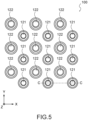
- Fig. 5 is a plan view of the light-emitting element array 100 in which illustration of the first wire 131 and the second wire 132 is omitted.
- Fig. 6 is a cross-sectional view of this light-emitting element array 100 and is a cross-sectional view taken along the line C-C in Fig. 5 .
- the light-emitting element array 100 includes a light-emitting element group configured by arraying a plurality of first light-emitting elements 121 and a plurality of second light-emitting elements 122 in a planar manner.
- a surface on which the first light-emitting element 121 and the second light-emitting element 122 are arrayed will be referred to as the light-emitting element surface 120
- one surface parallel to the light-emitting element surface 120 will be referred to as the X direction
- a direction that is parallel to the light-emitting element surface 120 and is orthogonal to the X direction will be referred to as the Y direction.
- the light-emitting element surface 120 is parallel to the X-Y plane. Further, a direction perpendicular to the light-emitting element surface 120 will be referred to as the Z direction.
- the number of the first light-emitting elements 121 and the number of the second light-emitting elements 122 are not particularly limited and can each be, for example, several tens to several thousands.
- the first light-emitting element 121 and the second light-emitting element 122 can be light-emitting elements having the same configuration.
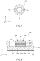
- Fig. 7 is a plan view of a light-emitting element 150 capable of constituting the first light-emitting element 121 and the second light-emitting element 122
- Fig. 8 is a cross-sectional view of the light-emitting element 150.
- the light-emitting element 150 is a vertical cavity surface emitting laser (VCSEL) element. As shown in Fig. 7 and Fig. 8 , the light-emitting element 150 has a mesa structure in which a mesa (plateau shape) 153 is formed by being surrounded by an annular recessed portion 152 provided on a substrate 151.
- VCSEL vertical cavity surface emitting laser
- the light-emitting element 150 includes an n-type DBR layer 154, an active layer 155, a current confinement layer 156, a p-type DBR layer 157, a p-electrode 158, and an n-electrode 159.
- the n-type DBR layer 154, the active layer 155, the current confinement layer 156, and the p-type DBR layer 157 are stacked on the substrate 151 in this order.
- the n-type DBR layer 154 is formed of an n-type semiconductor material, functions as a DBR (Distributed Bragg Reflector), and reflects light having a specific wavelength (hereinafter, the wavelength ⁇ ).
- the n-type DBR layer 154 constitutes an optical resonator for laser oscillation together with the p-type DBR layer 157.
- the active layer 155 is provided between the n-type DBR layer 154 and the p-type DBR layer 157, and emits and amplifies spontaneously emitted light.
- the active layer 155 can include a plurality of layers obtained by alternately stacking a quantum well layer and a barrier layer.
- the current confinement layer 156 is provided in the vicinity of the active layer 155 and imparts a confinement action to a current.
- the current confinement layer 156 includes a non-oxidized region 156a and an oxidized region 156b.
- the non-oxidized region 156a is provided in the center of the current confinement layer 156 and the oxidized region 156b is provided around the non-oxidized region 156a.
- the oxidized region 156b can be formed by performing oxidation treatment from the outer periphery side of a mesa 153 via the recessed portion 152.
- the p-type DBR layer 157 is formed of a p-type semiconductor material, functions as a DBR, and reflects light having the wavelength ⁇ .
- the p-type DBR layer 157 constitutes an optical resonator for laser oscillation together with the n-type DBR layer 154.
- the p-electrode 158 is provided on the surface of the mesa 153 and is electrically connected to the p-type DBR layer 157. As shown in Fig. 7 , the p-electrode 158 has an annular shape.
- the n-electrode 159 is provided on the surface of the substrate 151 on the side opposite to the light-emitting element 150 and is electrically connected to the n-type DBR layer 154 via the substrate 151.
- the light-emitting element 150 has the configuration as described above.
- a voltage is applied between the p-electrode 158 and the n-electrode 159
- a current flows between the p-electrode 158 and the n-electrode 159.
- the current is subjected to a current confinement action by the current confinement layer 156 and is injected into the active layer 155 in the vicinity of the non-oxidized region 156a.
- This injected current causes spontaneously emitted light in the active layer 155, and the spontaneously emitted light is reflected by the n-type DBR layer 154 and the p-type DBR layer 157.
- a component of the oscillation wavelength X forms a standing wave between the n-type DBR layer 154 and the p-type DBR layer 157 and is amplified by the active layer 155.
- the injected current exceeds a threshold value, laser oscillation of light forming a standing wave occurs, and a laser beam passes through the p-type DBR layer 157 and is emitted.
- a surface from which a laser beam is emitted is shown as a light-emitting surface S.
- the p-electrode 158 is provided around the light-emitting surface S.
- the configuration of the light-emitting element 150 is not limited to the one shown here.
- the n-type and the p-type in the light-emitting element 150 may be reversed.
- the configuration described above shows the configuration of a surface emission type VCSEL element
- the light-emitting element 150 may be a backside emission type VCSEL.
- the light-emitting element 150 is not limited to the VCSEL and may be a light-emitting element formed of a semiconductor such as an LED (Light Emitting Diode).
- the light-emitting element array 100 can be a light-emitting element array in which the first light-emitting element 121 and the second light-emitting element 122, each of which has the configuration of the light-emitting element 150, are arrayed.
- the size of the mesa 153 may differ or may be the same.
- the first light-emitting element 121 and the second light-emitting element 122 have the configurations as described above.
- the first light-emitting element 121 and the second light-emitting element 122 are configured to be capable of emitting light independently of each other.
- the n-electrode 159 is uniformly formed on the back surface of the substrate 151 and is a common electrode between the first light-emitting element 121 and the second light-emitting element 122.
- the p-electrode 158 is provided on each mesa 153 and is an independent electrode for each of the first light-emitting element 121 and the second light-emitting element 122. Therefore, when a voltage is applied between the p-electrode 158 and the n-electrode 159 provided in the first light-emitting element 121, the first light-emitting element 121 can be caused to emit light. When a voltage is applied between the p-electrode 158 and the n-electrode 159 provided in the second light-emitting element 122, the second light-emitting element 122 can be caused to emit light. Note that in the figures other than Fig. 8 , illustration of the layer structure of the light-emitting element 150 is omitted and only the p-electrode 158 is illustrated.
- an insulation layer 161 is provided on the light-emitting element surface 120.
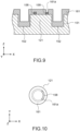
- Fig. 9 is a cross-sectional view showing the insulation layer 161 on the first light-emitting element 121
- Fig. 10 is a plan view of the insulation layer 161 on the first light-emitting element 121.
- a first through hole 161a is provided in the insulation layer 161 on the first light-emitting element 121. The first through hole 161a penetrates the insulation layer 161 and exposes part of the p-electrode 158 of the first light-emitting element 121.
- Fig. 11 is a cross-sectional view showing the insulation layer 161 on the second light-emitting element 122
- Fig. 12 is a plan view of the insulation layer 161 on the second light-emitting element 122.
- a second through hole 161b is provided in the insulation layer 161 on the second light-emitting element 122.
- the second through hole 161b penetrates the insulation layer 161 and exposes part of the p-electrode 158 of the second light-emitting element 122. Note that in Fig. 1 , Fig. 2 , and Fig. 5 , illustration of the insulation layer 161 is omitted.
- the first wire 131 and the second wire 132 are each formed of a conductive material such as Au and are formed in the same layer as shown in Fig. 3 and Fig. 4 . Further, as shown in Fig. 1 to Fig. 4 , the first wire 131 and the second wire 132 extend in parallel to the light-emitting element surface (X-Y plane) 120 and are separated from each other.
- the first wire 131 and the second wire 132 each have regions overlapping with the first light-emitting element 121 and the second light-emitting element 122 as viewed from a direction (the Z direction) perpendicular to the light-emitting element surface 120.
- the regions of the first wire 131 and the second wire 132 overlapping with the first light-emitting element 121 are shown as regions R1
- the regions of the first wire 131 and the second wire 132 overlapping with the second light-emitting element 122 are shown as regions R2.
- both the first wire 131 and the second wire 132 have the region R1 and the region R2.
- the region R1 and the region R2 are formed on the outer periphery side than the p-electrode 158 so as not to shield the light-emitting surface S (see Fig. 8 ).
- the region R1 and the region R2 may be formed on the inner periphery side than the p-electrode 158 as long as the light-emitting surface S is not shielded. Further, in the case of prioritizing the increase in the width of the first wire 131 and the second wire 132, the region R1 and the region R2 can be formed so as to partially shield the light-emitting surface S.
- the first wire 131 is electrically connected to the first light-emitting element 121
- the second wire 132 is electrically connected to the second light-emitting element 122.
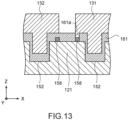
- Fig. 13 is a cross-sectional view showing a connection relationship between the first light-emitting element 121 and the first wire 131 and the second wire 132. As shown in the figure, the first wire 131 comes into contact with the p-electrode 158 of the first light-emitting element 121 via the first through hole 161a and is electrically connected to the p-electrode 158 of the first light-emitting element 121.
- the second wire 132 is insulated from the p-electrode 158 of the first light-emitting element 121 by the insulation layer 161 provided between the second wire 132 and the p-electrode 158 of the first light-emitting element 121.
- the other first light-emitting elements 121 included in the light-emitting element array 100 are each electrically connected to the first wire 131 and insulated from the second wire 132.
- Fig. 14 is a cross-sectional view showing a connection relationship between the second light-emitting element 122 and the first wire 131 and the second wire 132.
- the second wire 132 comes into contact with the p-electrode 158 of the second light-emitting element 122 vis the second through hole 161b and is electrically connected to the p-electrode 158 of the second light-emitting element 122.
- the first wire 131 is insulated from the p-electrode 158 of the second light-emitting element 122 by the insulation layer 161 provided between the first wire 131 and the p-electrode 158 of the second light-emitting element 122.
- the other second light-emitting elements 122 included in the light-emitting element array 100 are each electrically connected to the second wire 132 and insulated from the first wire 131.
- Fig. 15 is a schematic diagram showing the array of the first light-emitting element 121 and the second light-emitting element 122.
- the first light-emitting elements 121 are arrayed along one direction (Y direction) in the light-emitting element surface 120 to form a plurality of light-emitting element columns L1.
- the second light-emitting elements 122 are arrayed along a direction (Y direction) parallel to the light-emitting element column L1 in the light-emitting element surface 120 to form a plurality of light-emitting element columns L2.
- the light-emitting element column L1 and the light-emitting element column L2 are alternately arranged and are separated from each other in a direction (X direction) orthogonal to the extending direction (Y direction).
- the line connecting the centers of the first light-emitting elements 121 to each other is shown as a center C1 of the light-emitting element column L1
- the line connecting the centers of the second light-emitting element 122 to each other is shown as a center C2 of the light-emitting element column L2.
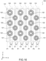
- Fig. 16 and Fig. 17 are each a schematic diagram showing the arrangement of the first wire 131 and the second wire 132.
- the first wire 131 and the second wire 132 are alternately provided between the center C1 of the light-emitting element column L1 and the center C2 of the light-emitting element column L2 as viewed from a direction (Z direction) perpendicular to the light-emitting element surface 120, extend along the extending direction (Y direction) of the light-emitting element column L1 and the light-emitting element column L2, and are separated from each other in a direction (X direction) orthogonal to the extending direction.
- one of the light-emitting element columns L1 is defined as a first light-emitting element column L1a
- the light-emitting element column L2 adjacent to the first light-emitting element column L1a is defined as a second light-emitting element column L2b
- the light-emitting element column L1 provided on the side opposite to the first light-emitting element column L1a with respect to the second light-emitting element column L2b is defined as a third light-emitting element column L1c.
- the first wire 131 is provided between the center C1 of the first light-emitting element column L1a and the center C2 of the second light-emitting element column L2b as viewed from the Z direction
- the second wire 132 is provided between the center C2 of the second light-emitting element column L2b and the center C1 of the third light-emitting element column L1c as viewed from the Z direction.
- the other first wires 131 and the other second wires 132 are arranged with respect to the light-emitting element columns L1 and the light-emitting element columns L2 such that a similar positional relationship is achieved.
- the center of the first wire 131 is defined as a center P1 and the center of the second wire 132 is defined as a center P2.
- the center P1 is offset in the X direction with respect to the center C1 as shown by an arrow A1 and is separated from the center C1.
- the center P2 is offset in the X direction with respect to the center C2 as shown by an arrow A2 and is separated from the center C2.
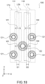
- Fig. 18 is a schematic diagram showing the widths of the first wire 131 and the second wire 132. As shown in the figure, the minimum width of the first wire 131 in the X direction is defined as a width W1 and the minimum width of the second wire 132 in the X direction is defined as a width W2.
- the interval between the first light-emitting element column L1a and the second light-emitting element column L2b in the X direction is defined as D1 and the interval between the second light-emitting element column L2b and the third light-emitting element column L1c in the X direction is defined as D2.
- the width W1 can be larger than the interval D1 and the width W2 can be larger than the interval D2.
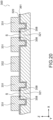
- Fig. 19 is a plan view of a light-emitting element array 300 according to a Comparative Example
- Fig. 20 is a cross-sectional view of the light-emitting element array 300.
- Fig. 20 is a cross-sectional view taken along the line D-D in Fig. 19 .
- the light-emitting element array 300 includes a first light-emitting element 321, a second light-emitting element 322, a first wire 331, and a second wire 332.
- the first light-emitting element 321 and the second light-emitting element 322 are arrayed in a planar manner to form a light-emitting element surface 320.
- the first light-emitting elements 321 and the second light-emitting elements 322 are each arrayed along one direction (Y direction) on the light-emitting element surface 320 to form a plurality of light-emitting element columns.
- the first wire 331 and the second wire 332 are formed on the light-emitting element surface 320 via an insulation layer 361.
- the first wire 331 extends on the column of the first light-emitting elements 321 and is electrically connected to a p-electrode 358 of the first light-emitting element 321 as shown in Fig. 20 .
- the first light-emitting element 321 emits light by the drive current supplied from the first wire 331.
- the first wire 331 is provided on the peripheral edge of the first light-emitting element 321 so as not to shield the light-emitting surface S on the first light-emitting element 321.
- the second wire 332 extends on the column of the second light-emitting elements 322 and is electrically connected to the p-electrode 358 of the second light-emitting element 322, similarly to the first wire 331.
- the second light-emitting element 322 emits light by the drive current supplied from the second wire 332.
- the second wire 332 is provided on the peripheral edge of the second light-emitting element 322 so as not to shield the light-emitting surface S on the second light-emitting element 322.
- the first wire 331 and the second wire 332 do not shield the light-emitting surface S and it is necessary to maintain the interval between adjacent wires in order to prevent a short circuit, it is difficult to increase the width of the wire. For this reason, when the number of arrays of light-emitting elements increases or the density of light-emitting elements increases, the influence of the wiring resistance becomes large and a problem that the amount of light emitted on the downstream side of the wire decreases occurs. Further, it is not easy to increase the thickness of the wire from the viewpoint of the production process.
- the first wire 131 and the second wire 132 are arranged so as to overlap with the first light-emitting element 121 and the second light-emitting element 122 (see Fig. 2 ).
- the widths of the first wire 131 and the second wire 132 are same as those in the Comparative Example, it is possible to bring the light-emitting elements and the wirings closer to each other and improve the density thereof. Further, since the first wire 131 and the second wire 132 are in the same layer, the production process is not complicated and it is possible to suppress the influence on the light-emitting properties.
- the light-emitting element array 100 may include groove portions for the first wire 131 and the second wire 132 in addition to the configuration described above.
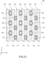
- Fig. 21 is a plan view of the light-emitting element array 100 including a groove portion
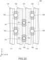
- Fig. 22 is an enlarged view of Fig. 21 .
- Fig. 23 is a cross-sectional view of this light-emitting element array 100 and is a cross-sectional view taken along the line E1 to E4 in Fig. 22 .
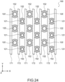
- Fig. 24 is a plan view of this light-emitting element array 100 in which illustration of the first wire 131 and the second wire 132 is omitted.
- a first groove portion 171 that connects between the recessed portions 152 (see Fig. 8 ) of the first light-emitting element 121 and a second groove portion 172 that connects between the recessed portions 152 (see Fig. 8 ) of the second light-emitting element 122 are provided in the substrate 151.
- the first groove portion 171 may be connected also to the recessed portion 152 of the second light-emitting element 122 and does not necessarily need to be connected thereto.
- the second groove portion 172 may be connected to the recessed portion 152 of the first light-emitting element 121 and does not necessarily need to be connected thereto.
- the first wire 131 is formed in the first groove portion 171 continuously from the recessed portion 152 of the first light-emitting element 121 and is continuous with the recessed portion 152 of the adjacent first light-emitting element.
- the second wire 132 is formed in the second groove portion 172 continuously from the recessed portion 152 of the second light-emitting element 122 and is continuous with the recessed portion 152 of the adjacent second light-emitting element.
- the thickness of each of the first wire 131 and the second wire 132 increases as compared with the case where the first groove portion 171 and the second groove portion 172 are not provided, and it is possible to further suppress the wiring resistance and contribute to the increase in the density of light-emitting elements and wires.
- the p-electrode 158 has an annular shape (see Fig. 7 ) as described above, the p-electrode 158 may have another shape.
- Fig. 25 to Fig. 31 are each a schematic diagram showing another shape of the p-electrode 158.
- the p-electrode 158 may have a rectangular annular shape as viewed from a direction (Z direction) perpendicular to the light-emitting element surface 120 as shown in Fig. 25 , or may have a hexagonal annular shape as viewed from the Z direction as shown in Fig. 26 . Further, the p-electrode 158 may have a polygonal shape or another annular shape as viewed from the Z direction.
- the p-electrode 158 may have a C-shape as viewed from a direction (Z direction) perpendicular to the light-emitting element surface 120 or may have various annular shapes from which part thereof is missing. Further, the p-electrode 158 may have a pair of arc shapes facing each other as viewed from the Z direction as shown in Fig. 28 or may have a pair of linear shapes facing each other as viewed from the Z direction as shown in Fig. 29 .
- the p-electrode 158 may have one arc shape as viewed from the Z direction as shown in Fig. 30 or may have one linear shape as viewed from the Z direction as shown in Fig. 31 .
- the p-electrode 158 is provided at a position overlapping with the first wire 131 or the second wire 132 to be connected (see Fig. 3 and Fig. 4 ) as viewed from the Z direction.
- the p-electrode 158 may have various shapes.
- the light-emitting element 150 has been described to include the mesa 153 having a cylindrical shape (see Fig. 7 ), the shape of the mesa 153 is not limited to a cylindrical shape.
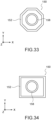
- Fig. 32 to Fig. 34 are each a schematic diagram showing another shape of the mesa 153.
- the mesa 153 may have a hexagonal column shape as shown in Fig. 32 or may have an octagonal column shape as shown in Fig. 33 . Further, the mesa 153 may have a quadrangular column shape as shown in Fig. 34 . In addition, the mesa 153 can have a polygonal column shape including a pentagonal column shape and a heptagonal column shape, or another columnar shape.
- Fig. 35 is a schematic diagram showing another configuration in the recessed portion 152.
- an embed material 162 may be embedded in the recessed portion 152 and may be covered with an insulation film 163.
- the first wire 131 and the second wire 132 can be formed on the insulation film 163. Further, in the case where the embed material 162 is formed of an insulating material, the insulation film 163 does not need to be provided.
- the embed material 162 may be used as the first wire 131 or the second wire 132 without providing the insulation film 163.
- the embed material 162 can be used as only one of the first wire 131 and the second wire 132, and the other wire needs to be provided on the insulation film 163.
- Fig. 36 and Fig. 37 are each a schematic diagram showing another arrangement of the first wire 131 and the second wire 132.
- the first wire 131 and the second wire 132 may be arranged as shown in these figures.
- the plurality of first wire 131 is adjacent to each other, the plurality of adjacent first wires 131 may be used as one first wire 131.
- the plurality of adjacent second wires 132 may be used as one second wire 132.
- the light-emitting element column L1 and the light-emitting element column L2 have been described as a linear column extending in the Y direction, the present technology is not limited thereto.
- the light-emitting element column L1 and the light-emitting element column L2 may extend in a curved shape, a spiral shape, a comb tooth shape, or the like.
- the first wire 131 and the second wire 132 each have the regions R1 and R2 (see Fig. 2 ) overlapping with the first light-emitting element 121 and the second light-emitting element 122 and make it possible to increase the density of light-emitting elements and wires.
- the light-emitting element array 100 can be used for a distance measurement light source device or the like capable of emitting short-distance light and long-distance light because the first light-emitting element 121 and the second light-emitting element 122 can be caused to independently emit light as described above.
- the light-emitting element group constituting the light-emitting element array 100 includes the first light-emitting element 121 and the second light-emitting element 122. Further, the light-emitting element group constituting the light-emitting element array 100 can include a third light-emitting element 123 and a fourth light-emitting element 124.
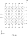
- Fig. 38 is a plan view of the light-emitting element array 100 that includes the third light-emitting element 123 and the fourth light-emitting element 124.
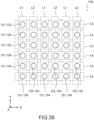
- the third light-emitting elements 123 are arrayed along one direction in the light-emitting element surface 120 to form a plurality of light-emitting element columns L3.
- the fourth light-emitting elements 124 are arrayed along a direction parallel to the light-emitting element column L3 in the light-emitting element surface 120 to form a plurality of light-emitting element columns L4.
- the light-emitting element column L3 and the light-emitting element column L4 are alternately arranged and are separated from each other in a direction orthogonal to the extending direction.
- Fig. 39 is a schematic diagram showing a relationship between the light-emitting element column L1 and the light-emitting element column L2 and the light-emitting element column L3 and the light-emitting element column L4. As shown in Fig. 39 , the light-emitting element column L3 and the light-emitting element column L4 extend in a direction (X direction) orthogonal to the extending direction (Y direction) of the light-emitting element column L1 and the light-emitting element column L2.
- the third light-emitting elements 123 include some of the first light-emitting elements 121 and some of the second light-emitting elements 122
- the fourth light-emitting elements 124 include the others of the first light-emitting element 121 and the others of the second light-emitting element 122.
- the first light-emitting element 121 and the second light-emitting element 122 are defined by whether the wire connected to the p-side (see Fig. 8 ) of each light-emitting element 150 is the first wire 131 or the second wire 132 as described above. Meanwhile, the third light-emitting element 123 and the fourth light-emitting element 124 are defined by the wire connected to the n-side of each light-emitting element 150 as described below. The wiring structure on this n-side will be described below.
- the electrical connection on the n-side can be made as follows.
- Fig. 40 is a plan view showing a wiring structure on the n-side of the light-emitting element array 100
- Fig. 41 is an enlarged view of Fig. 40
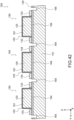
- Fig. 42 is a cross-sectional view of the light-emitting element array 100 and is a cross-sectional view taken along the line E-E in Fig. 41 .
- the light-emitting element array 100 includes a third wire 133 and a fourth wire 134 as n-side wires. Note that in Fig. 40 to Fig. 42 , illustration of a partial configuration such as the p-electrode 158, the first wire 131, and the second wire 132 is omitted.
- the third light-emitting element 123 and the fourth light-emitting element 124 each have a mesa structure in which the mesa (plateau shape) 153 is formed by being surrounded by the recessed portion 152 provided in the substrate 151.
- the recessed portion 152 has a bottom surface 125 that is separated from the light-emitting element surface 120 (see Fig. 6 ) and is parallel to the light-emitting element surface 120.
- the bottom surface 125 is a surface formed by an n-contact layer 164.
- the n-contact layer 164 is formed of an n-type semiconductor material and is provided adjacent to the n-type DBR layer 154 on the substrate 151 side of the n-type DBR layer 154.
- An element isolation groove 165 is provided in the bottom surface 125.
- the element isolation groove 165 is provided between the light-emitting element column L3 and the light-emitting element column L4 and extend along the extending direction of the light-emitting element column L3 and the light-emitting element column L4.
- the element isolation groove 165 has a depth at which at least the n-contact layer 164 can be separated and electrically separates the third light-emitting element 123 and the fourth light-emitting element 124 from each other by separating the n-contact layer 164.
- the third wire 133 and the fourth wire 134 are each formed of a conductive material such as Au and is formed on the bottom surface 125.
- the third wire 133 is provided between the element isolation grooves 165 and around the third light-emitting element 123 as viewed from a direction (Z direction) perpendicular to the bottom surface 125 and extends along the extending direction (X direction) of the light-emitting element column L3.
- the fourth wire 134 is provided between the element isolation grooves 165 and around the fourth light-emitting element 124 as viewed from a direction (Z direction) perpendicular to the bottom surface 125 and extends along the extending direction (X direction) of the light-emitting element column L4.
- the third wire 133 and the fourth wire 134 have the configuration as described above, it is possible to switch the light-emitting element 150 that emits light. Specifically, by applying a voltage between the first wire 131 and the third wire 133, it is possible to cause the light-emitting element 150 (see Fig. 39 ) included in both the light-emitting element column L1 and the light-emitting element column L3 to emit light.
- the widths of the third wire 133 and the fourth wire 134 will be examined.
- the minimum width of the third wire 133 in the Y direction is defined as a width W3 and the minimum width of the fourth wire 134 in the Y direction is defined as a width W4.
- the width W3 and the width W4 are widened, the density of light-emitting elements decreases and the light emission intensity of the light-emitting element array 100 is reduced.
- a configuration the width W3 and the width W4 are widened while maintaining the density of light-emitting elements will be described.
- the structure described above can be formed by etching the mesa 153 up to the n-contact layer 164 by RIE (Reactive Ion Etching). After that, the mesa 153 is covered with the insulation layer 161 and the insulation layer 161 around the mesa 153 is further opened by RIE. As a result, the bottom surface 125 is exposed, so that the third wire 133 and the fourth wire 134 can be formed on the bottom surface 125.
- RIE Reactive Ion Etching
- Fig. 43 is a plan view showing this wiring structure
- Fig. 44 is an enlarged view of Fig. 43
- Fig. 45 is a cross-sectional view of the light-emitting element array 100, and is a cross-sectional view taken along the line F-F in Fig. 44 . Note that in Fig. 43 to Fig. 45 , illustration of a partial configuration such as the p-electrode 158, the first wire 131, and the second wire 132 is omitted. As shown in Fig. 43 and Fig.
- the third wire 133 and the fourth wire 134 are each arranged between the light-emitting element column L3 and the light-emitting element column L4. Further, as shown in Fig. 45 , the third wire 133 and the fourth wire 134 are provided on the bottom surface 125 and the element isolation groove 165.
- Fig. 46 is a plan view showing the bottom surface 125
- Fig. 47 is a cross-sectional view taken along the line G-G in Fig. 46 .
- a region of the bottom surface 125 between the element isolation groove 165 and the third light-emitting element 123 is defined as a region R3.
- a region of the bottom surface 125 between the element isolation groove 165 and the fourth light-emitting element 124 is defined as a region R4.
- Fig. 48 is a plan view showing the insulation layer 161
- Fig. 49 is a cross-sectional view taken along the line H-H in Fig. 48 .
- a first opening 161c that is an opening of the insulation layer 161 is provided on one of the regions R3 (see Fig. 47 ) on both sides of the third light-emitting element 123.
- a second opening 161d that is an opening of the insulation layer 161 is provided on one of the regions R4 (see Fig. 47 ) on both sides of the fourth light-emitting element 124.
- the third wire 133 is provided on the insulation layer 161 and in the element isolation groove 165, which are provided on the bottom surface 125, and overlaps with the region R3, the region R4, and the element isolation groove 165 as viewed from a direction (Z direction) perpendicular to the bottom surface 125.
- the third wire 133 comes into contact with the n-contact layer 164 of the third light-emitting element 123 via the first opening 161c provided on the region R3 and is electrically connected to the n-contact layer 164 of the third light-emitting element 123.
- the third wire 133 is insulated from the n-contact layer 164 of the fourth light-emitting element 124 by the insulation layer 161 on the region R4.
- the fourth wire 134 is provided on the insulation layer 161 and in the element isolation groove 165, which are provide on the bottom surface 125, and overlaps with the region R3, the region R4, and the element isolation groove 165 as viewed from a direction (Z direction) perpendicular to the bottom surface 125.
- the fourth wire 134 comes into contact with the n-contact layer 164 of the fourth light-emitting element 124 via the second opening 161d provided on the region R4 and is electrically connected to the n-contact layer 164 of the fourth light-emitting element 124.
- the fourth wire 134 is insulated from the n-contact layer 164 of the third light-emitting element 123 by the insulation layer 161 on the region R3.
- the minimum width W3 of the third wire 133 in the Y direction and the minimum width W4 of the fourth wire 134 in the Y direction can be widened while maintaining the density of light-emitting elements. As a result, it is possible to reduce the wiring resistance of the third wire 133 and the fourth wire 134.
- the structure described above can be formed by etching the mesa 153 up to the n-contact layer 164 by RIE. After that, the mesa 153 is covered with the insulation layer 161, and the first opening 161c and the second opening 161d are formed by RIE. As a result, it is possible to form the third wire 133 on the first opening 161c and the insulation layer 161 and form the fourth wire 134 on the second opening 161d and the insulation layer 161.
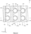
- Fig. 50 is a plan view showing this wiring structure
- Fig. 51 is an enlarged view of Fig. 50 .
- the cross-sectional view taken along the line I-I of this light-emitting element array 100 is the same as that in Fig. 45 .
- illustration of a partial configuration such as the p-electrode 158, the first wire 131, and the second wire 132 is omitted.
- the third wire 133 and the fourth wire 134 are different from the third wire 133 and the fourth wire 134 (see Fig. 43 ) shown in the wiring structure 2 in the separation positions of the wires.
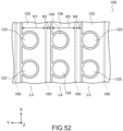
- Fig. 52 is a plan view showing the shapes of the third wire 133 and the fourth wire 134.
- the width of the third wire 133 in the Y direction from the element isolation groove 165 to the third light-emitting element 123 side is defined as a width K1
- the width of the third wire 133 in the Y direction from the element isolation groove 165 to the fourth light-emitting element 124 side is defined as a width K2
- the width K1 is larger than the width K2.
- the width of the fourth wire 134 in the Y direction from the element isolation groove 165 to the fourth light-emitting element 124 side is defined as a width K3 and the width of the fourth wire 134 in the Y direction from the element isolation groove 165 to the third light-emitting element 123 side is defined as a width K4, the width K3 is larger than the width K4.
- the opening areas of the first opening 161c and the second opening 161d can be increased as shown in Fig. 51 while the minimum width W3 of the third wire 133 and the minimum width W4 of the fourth wire 134 are the same as those in the wiring structure 2.
- Fig. 53 is a schematic diagram showing another extending direction of the light-emitting element column L3 and the light-emitting element column L4.
- the extending direction of the light-emitting element column L3 and the light-emitting element column L4 can be the Y direction that is the same as the extending direction of the light-emitting element column L1 and the light-emitting element column L2.
- the third light-emitting element 123 coincides with the first light-emitting element 121 and the fourth light-emitting element 124 coincides with the second light-emitting element 122.
- the light-emitting element 150 included in the light-emitting element column L1 (same as the light-emitting element column L3) can be caused to emit light by applying a voltage between the first wire 131 and the third wire 133.
- the light-emitting element 150 included in the light-emitting element column L2 (same as the light-emitting element column L4) can be caused to emit light.
- the extending direction of the light-emitting element column L3 and the light-emitting element column L4 can be any direction parallel to the X-Y plane.
- the first wire 131 and the second wire 132 that are p-side wires have had a configuration according to the present technology (see Fig. 2 ) and the third wire 133 and the fourth wire 134 that are n-side wires also have had a configuration according to the present technology (see Fig. 45 ).
- both the wires on the p-side and the n-side do not necessarily need to have a configuration according to the present technology. That is, in the light-emitting element array 100, only the p-side wire may have a configuration according to the present technology and the n-side wire may have a general wiring structure in a light-emitting element array. Further, in the light-emitting element array 100, only the n-side wire may have a configuration according to the present technology and the p-side wire may have a general wiring structure in a light-emitting element array.
- first wire 131 and the second wire 132 have been the p-side wires and the third wire 133 and the fourth wire 134 have been the n-side wires in the above description, the n-type and the p-type in the light-emitting element 150 may be reversed.
- the first wire 131 and the second wire 132 are n-side wires and the third wire 133 and the fourth wire 134 are p-side wires.
- the effects described in the present disclosure are merely examples and are not limited, and additional effects may be exerted.
- the description of the plurality of effects described above does not necessarily mean that these effects are exerted at the same time. It means that at least one of the effects described above can be achieved and there is a possibility that an effect that is not described in the present disclosure is exerted. Further, at least two feature parts of the feature parts described in the present disclosure may be arbitrarily combined with each other.
Landscapes
- Physics & Mathematics (AREA)
- Condensed Matter Physics & Semiconductors (AREA)
- General Physics & Mathematics (AREA)
- Electromagnetism (AREA)
- Optics & Photonics (AREA)
- Led Devices (AREA)
- Semiconductor Lasers (AREA)
Abstract
Description
- The present technology relates to a light-emitting element array in which a plurality of light-emitting elements is arrayed.
- A light-emitting element such as a vertical cavity surface emitting laser (VCSEL) element is often used as a light-emitting element array in which a plurality of light-emitting elements is arrayed. Here, in the light-emitting element array, wiring of each light-emitting element causes a problem in accordance with the number and density of light-emitting elements constituting the array.
- For example,
Patent Literature 1 discloses an image forming apparatus in which an anode wire and a cathode wire are connected to each of a large number of light-emitting elements arrayed in a matrix. The anode wire and the cathode wire are provided so as to extend in directions orthogonal to each other and intersect with each other and configured such that the size of the light-emitting unit can be reduced and the size of the individual light-emitting element can be increased. - Further, Patent Literature 2 discloses an image forming apparatus in which a first wire and a second wire are connected to each of a large number of light-emitting element arranged in an n×m matrix. N or more first wires are provided and n or more second wires intersecting with the first wires are provided, so that the wiring resistance and the electrostatic capacity of each wire can be suppressed.
-
- Patent Literature 1:
Japanese Patent Application Laid-open No. 2001-063139 - Patent Literature 2:
Japanese Patent Application Laid-open No. 1998-107386 - However, in the configuration described in
Patent Literature 1, the space for providing wires is limited as the interval between light-emitting elements is reduced and it is difficult to form wires. Further, the configuration described in Patent Literature 2 has a problem that the operation delay increases as the density of the light-emitting elements increases. As described above, the existing technology has not sufficiently dealt with the increase in density of light-emitting elements from the viewpoint of the wiring structure. - In view of the circumstances as described above, it is an object of the present technology to provide a light-emitting element array having a wiring structure making it possible to increase the density of light-emitting elements.
- In order to achieve the above-mentioned object, a light-emitting element array according to an embodiment of the present technology includes: a light-emitting element group; a first wire; and a second wire.
- The light-emitting element group includes a plurality of first light-emitting elements and a plurality of second light-emitting elements that are arrayed in a planar manner to form a light-emitting element surface.
- The first wire extends in a direction parallel to the light-emitting element surface, has a region overlapping with the plurality of first light-emitting elements and a region overlapping with the plurality of second light-emitting elements as viewed from a direction perpendicular to the light-emitting element surface, is electrically connected to the plurality of first light-emitting elements, and is not electrically connected to the plurality of second light-emitting elements.
- The second wire extends in a direction parallel to the light-emitting element surface, has a region overlapping with the plurality of first light-emitting elements and a region overlapping with the plurality of second light-emitting elements as viewed from a direction perpendicular to the light-emitting element surface, is electrically connected to the plurality of second light-emitting elements, and is not electrically connected to the plurality of first light-emitting elements.
- In accordance with this configuration, since each of the first wire and the second wire has the regions overlapping with the first light-emitting element and the second light-emitting element, the first wire is electrically connected to only the first light-emitting element, and the second wire is electrically connected to only the second light-emitting element, it is possible to make the first wire and the second wire independently emit light while increasing the density of the first wires and the second wires.
- The light-emitting element group may include a first light-emitting element column in which the plurality of first light-emitting elements is arrayed, and a second light-emitting element column in which the plurality of second light-emitting elements is arrayed,
- a center of the first wire may be separated from a center of the first light-emitting element column in a direction parallel to the light-emitting element surface, and
- a center of the second wire may be separated from a center of the second light-emitting element column in a direction parallel to the light-emitting element surface.
- The light-emitting element group may further include a third light-emitting element column in which the plurality of first light-emitting elements is arrayed, the third light-emitting element column being provided on a side opposite to the first light-emitting element column with respect to the second light-emitting element column,
- the first wire may be provided between the center of the first light-emitting element column and the center of the second light-emitting element column as viewed from a direction perpendicular to the light-emitting element surface, and
- the second wire may be provided between the center of the second light-emitting element column and a center of the third light-emitting element column as viewed from a direction perpendicular to the light-emitting element surface.
- The first light-emitting element column, the second light-emitting element column, the third light-emitting element column, the first wire, and the second wire may each extend in a first direction parallel to the light-emitting element surface and are separated from each other in a second direction that is parallel to the light-emitting element surface and orthogonal to the first direction,
- a width of the first wire in the second direction may be larger than an interval between the first light-emitting element column and the second light-emitting element column in the second direction, and
- a width of the second wire in the second direction may be larger than an interval between the second light-emitting element column and the third light-emitting element column in the second direction.
- The first wire and the second wire may be formed in a same layer.
- The first wire may be stacked on the plurality of first light-emitting elements and the plurality of second light-emitting elements via an insulation layer, be electrically connected to the plurality of first light-emitting elements via a first through hole provided in the insulation layer on the plurality of first light-emitting elements, and be insulated from the plurality of second light-emitting elements by the insulation layer on the plurality of second light-emitting elements, and
the second wire may be stacked on the plurality of first light-emitting elements and the plurality of second light-emitting elements via the insulation layer, be electrically connected to the plurality of second light-emitting elements via a second through hole provided in the insulation layer on the plurality of second light-emitting elements, and be insulated from the plurality of first light-emitting elements by the insulation layer on the plurality of first light-emitting elements. - The plurality of first light-emitting elements may each be a vertical cavity surface emitting laser element and include a first light-emitting surface and a first electrode provided around the first light-emitting surface,
- the plurality of second light-emitting elements may each be a vertical cavity surface emitting laser element and include a second light-emitting surface and a second electrode provided around the second light-emitting surface,
- the first wire may abut on the first electrode via the first through hole in the plurality of first light-emitting elements, and
- the second wire may abut on the second electrode via the second through hole in the plurality of second light-emitting elements.
- The plurality of first light-emitting elements and the plurality of second light-emitting elements may each have a mesa structure surrounded by a recessed portion,
- the light-emitting element group may include a first groove portion that connects the recessed portions to each other between the plurality of first light-emitting elements and a second groove portion that connects the recessed portions to each other between the plurality of second light-emitting elements,
- the first wire may have a portion formed in the first groove portion, and
- the second wire may have a portion formed in the second groove portion.
- The light-emitting elements constituting the light-emitting element group may include a plurality of third light-emitting elements and a plurality of fourth light-emitting elements, the plurality of third light-emitting elements and the plurality of fourth light-emitting elements each having a mesa structure surrounded by a recessed portion, the recessed portion being separated from the light-emitting element surface and having a bottom surface parallel to the light-emitting element surface, an element isolation groove that electrically separates the plurality of third light-emitting elements and the plurality of fourth light-emitting elements from each other being provided in the bottom surface, and
the light-emitting element array may further include: - a third wire that extends in a direction parallel to the bottom surface, has a region of the bottom surface between the element isolation groove and the third light-emitting element and a region of the bottom surface between the element isolation groove and the fourth light-emitting element as viewed from a direction perpendicular to the bottom surface, overlaps with the element isolation groove, is electrically connected to the third light-emitting element, and is not electrically connected to the fourth light-emitting element; and
- a fourth wire that extends in a direction parallel to the bottom surface, has a region of the bottom surface between the element isolation groove and the third light-emitting element and a region of the bottom surface between the element isolation groove and the fourth light-emitting element as viewed from a direction perpendicular to the bottom surface, overlaps with the element isolation groove, is electrically connected to the fourth light-emitting element, and is not electrically connected to the third light-emitting element.
- The light-emitting element group may include a first light-emitting element column in which the plurality of first light-emitting elements is arrayed, a second light-emitting element column in which the plurality of second light-emitting elements is arrayed, a third light-emitting element column in which the plurality of third light-emitting elements is arrayed, and a fourth light-emitting element column in which the plurality of fourth light-emitting elements is arrayed.
- The first light-emitting element column, the second light-emitting element column, the first wire, and the second wire may each extend in a first direction parallel to the light-emitting element surface, and
the third light-emitting element column, the fourth light-emitting element column, the third wire, and the fourth wire may each extend in a second direction that is parallel to the light-emitting element surface and is orthogonal to the first direction. - The first light-emitting element column, the second light-emitting element column, the first wire, and the second wire may each extend in a first direction parallel to the light-emitting element surface, and
the third light-emitting element column, the fourth light-emitting element column, the third wire, and the fourth wire may each extend in the first direction. - The third wire may be stacked on the bottom surface and the element isolation groove via an insulation layer, be electrically connected to the plurality of third light-emitting elements via a first opening provided in the insulation layer in a region of the bottom surface between the element isolation groove and the third light-emitting element, and be insulated from the plurality of fourth light-emitting elements by the insulation layer in a region of the bottom surface between the element isolation groove and the fourth light-emitting element, and
the fourth wire may be stacked on the bottom surface and the element isolation groove via the insulation layer, be electrically connected to the plurality of fourth light-emitting elements via a second opening provided in the insulation layer in a region of the bottom surface between the element isolation groove and the fourth light-emitting element, and be insulated from the plurality of third light-emitting elements by the insulation layer in a region of the bottom surface between the element isolation groove and the third light-emitting element. - The third wire may have a width from the element isolation groove to a side of the third light-emitting element larger than a width from the element isolation groove to a side of the fourth light-emitting element, and
the fourth wire may have a width from the element isolation groove to a side of the fourth light-emitting element larger than a width from the element isolation groove to a side of the third light-emitting element. - In order to achieve the above-mentioned object, a light-emitting element array according to an embodiment of the present technology includes: a light-emitting element group; a first wire; and a second wire.
- The light-emitting element group is a light-emitting element group in which a plurality of first light-emitting elements and a plurality of second light-emitting elements are arrayed in a planar manner to form a light-emitting element surface, the plurality of first light-emitting elements and the plurality of second light-emitting elements each having a mesa structure surrounded by a recessed portion, the recessed portion being separated from the light-emitting element surface and having a bottom surface parallel to the light-emitting element surface, an element isolation groove that electrically separates the plurality of first light-emitting elements and the plurality of second light-emitting elements from each other being provided in the bottom surface.
- The first wire extends in a direction parallel to the bottom surface, has a region of the bottom surface between the element isolation groove and the first light-emitting element and a region of the bottom surface between the element isolation groove and the second light-emitting element as viewed from a direction perpendicular to the bottom surface, overlaps with the element isolation groove, is electrically connected to the first light-emitting element, and is not electrically connected to the second light-emitting element.
- The second wire extends in a direction parallel to the bottom surface, has a region of the bottom surface between the element isolation groove and the first light-emitting element and a region of the bottom surface between the element isolation groove and the second light-emitting element as viewed from a direction perpendicular to the bottom surface, overlaps with the element isolation groove, is electrically connected to the second light-emitting element, and is not electrically connected to the first light-emitting element.
-
- [
Fig. 1] Fig. 1 is a plan view of a light-emitting element array according to an embodiment of the present technology. - [
Fig. 2] Fig. 2 is an enlarged plan view of the light-emitting element array. - [
Fig. 3] Fig. 3 is a cross-sectional view of the light-emitting element array. - [
Fig. 4] Fig. 4 is a cross-sectional view of the light-emitting element array. - [
Fig. 5] Fig. 5 is a plan view of a partial configuration of the light-emitting element array. - [
Fig. 6] Fig. 6 is a cross-sectional view of a partial configuration of the light-emitting element array. - [
Fig. 7] Fig. 7 is a plan view of a light-emitting element constituting the light-emitting element array. - [
Fig. 8] Fig. 8 is a cross-sectional view of the light-emitting element constituting the light-emitting element array. - [
Fig. 9] Fig. 9 is a cross-sectional view showing an insulation layer included in the light-emitting element array. - [
Fig. 10] Fig. 10 is a plan view showing the insulation layer included in the light-emitting element array. - [
Fig. 11] Fig. 11 is a cross-sectional view showing the insulation layer included in the light-emitting element array. - [
Fig. 12] Fig. 12 is a plan view showing the insulation layer included in the light-emitting element array. - [
Fig. 13] Fig. 13 is a cross-sectional view showing a connection relationship between a first light-emitting element, a first wire, and a second wire in the light-emitting element array. - [
Fig. 14] Fig. 14 is a cross-sectional view showing a connection relationship between a second light-emitting element, the first wire, and the second wire in the light-emitting element array. - [
Fig. 15] Fig. 15 is a plan view showing a light-emitting element column in the light-emitting element array. - [
Fig. 16] Fig. 16 is a plan view showing a positional relationship between the light-emitting element column, the first wire, and the second wire in the light-emitting element array. - [
Fig. 17] Fig. 17 is a plan view showing a positional relationship between first to third light-emitting element columns, the first wire, and the second wire in the light-emitting element array. - [
Fig. 18] Fig. 18 is a plan view showing widths of the first wire and the second wire in the light-emitting element array. - [
Fig. 19] Fig. 19 is a plan view of a light-emitting element array according to a Comparative Example. - [
Fig. 20] Fig. 20 is a cross-sectional view of the light-emitting element array according to the Comparative Example. -
Fig. 21] Fig. 21 is a plan view of a light-emitting element array in which a groove portion is provided according to an embodiment of the present technology. - [
Fig. 22] Fig. 22 is an enlarged plan view of the light-emitting element array. - [
Fig. 23] Fig. 23 is a cross-sectional view of the light-emitting element array. - [
Fig. 24] Fig. 24 is a plan view of a partial configuration of the light-emitting element array. - [
Fig. 25] Fig. 25 is a plan view of a light-emitting element constituting a light-emitting element array according to a modified example of the present technology. - [
Fig. 26] Fig. 26 is a plan view of the light-emitting element constituting the light-emitting element array according to the modified example of the present technology. - [
Fig. 27] Fig. 27 is a plan view of the light-emitting element constituting the light-emitting element array according to the modified example of the present technology. - [
Fig. 28] Fig. 28 is a plan view of the light-emitting element constituting the light-emitting element array according to the modified example of the present technology. - [
Fig. 29] Fig. 29 is a plan view of the light-emitting element constituting the light-emitting element array according to the modified example of the present technology. - [
Fig. 30] Fig. 30 is a plan view of the light-emitting element constituting the light-emitting element array according to the modified example of the present technology. - [
Fig. 31] Fig. 31 is a plan view of the light-emitting element constituting the light-emitting element array according to the modified example of the present technology. - [
Fig. 32] Fig. 32 is a plan view of the light-emitting element constituting the light-emitting element array according to the modified example of the present technology. - [
Fig. 33] Fig. 33 is a plan view of the light-emitting element constituting the light-emitting element array according to the modified example of the present technology. - [
Fig. 34] Fig. 34 is a plan view of the light-emitting element constituting the light-emitting element array according to the modified example of the present technology. - [
Fig. 35] Fig. 35 is a cross-sectional view of the light-emitting element array according to the modified example of the present technology. - [
Fig. 36] Fig. 36 is a plan view of the light-emitting element array according to the modified example of the present technology. - [
Fig. 37] Fig. 37 is a plan view of the light-emitting element array according to the modified example of the present technology. - [
Fig. 38] Fig. 38 is a plan view of a light-emitting element array that includes a third light-emitting element and a fourth light-emitting element according to an embodiment of the present technology. - [
Fig. 39] Fig. 39 is a schematic diagram showing a light-emitting element column of the light-emitting element array. - [
Fig. 40] Fig. 40 is a plan view of the light-emitting element array showing a third wire and a fourth wire. - [
Fig. 41] Fig. 41 is an enlarged plan view of the light-emitting element array showing the third wire and the fourth wire. - [
Fig. 42] Fig. 42 is a cross-sectional view of the light-emitting element array showing the third wire and the fourth wire. - [
Fig. 43] Fig. 43 is a plan view of the light-emitting element array showing the third wire and the fourth wire. - [
Fig. 44] Fig. 44 is an enlarged plan view of the light-emitting element array showing the third wire and the fourth wire. - [
Fig. 45] Fig. 45 is a cross-sectional view of the light-emitting element array showing the third wire and the fourth wire. - [
Fig. 46] Fig. 46 is a plan view of the light-emitting element array showing a bottom surface of a recessed portion. - [
Fig. 47] Fig. 47 is a cross-sectional view of the light-emitting element array showing the bottom surface of the recessed portion. - [
Fig. 48] Fig. 48 is a plan view of the light-emitting element array showing an opening of an insulation layer. - [
Fig. 49] Fig. 49 is a cross-sectional view of the light-emitting element array showing the opening of the insulation layer. - [
Fig. 50 ]Fig. 40 is a plan view of the light-emitting element array showing the third wire and the fourth wire. - [
Fig. 51] Fig. 51 is an enlarged plan view of the light-emitting element array showing the third wire and the fourth wire. - [
Fig. 52] Fig. 52 is an enlarged plan view of the light-emitting element array showing the third wire and the fourth wire. - [
Fig. 53] Fig. 53 is a schematic diagram showing a light-emitting element column of the light-emitting element array. - A light-emitting element array according to an embodiment of the present technology will be described.
-
Fig. 1 is a plan view of a light-emittingelement array 100 according to this embodiment, andFig. 2 is an enlarged view ofFig. 1 .Fig. 3 andFig. 4 are each a cross-sectional view of the light-emittingelement array 100.Fig. 3 is a cross-sectional view taken along the line A-A inFig. 2 , andFig. 4 is a cross-sectional view taken along the line B-B inFig. 2 . As shown in these figures, the light-emittingelement array 100 includes a first light-emittingelement 121, a second light-emittingelement 122, afirst wire 131, and asecond wire 132. -
Fig. 5 is a plan view of the light-emittingelement array 100 in which illustration of thefirst wire 131 and thesecond wire 132 is omitted.Fig. 6 is a cross-sectional view of this light-emittingelement array 100 and is a cross-sectional view taken along the line C-C inFig. 5 . - As shown in
Fig. 5 , the light-emittingelement array 100 includes a light-emitting element group configured by arraying a plurality of first light-emittingelements 121 and a plurality of second light-emittingelements 122 in a planar manner. Hereinafter, as shown inFig. 6 , a surface on which the first light-emittingelement 121 and the second light-emittingelement 122 are arrayed will be referred to as the light-emittingelement surface 120, one surface parallel to the light-emittingelement surface 120 will be referred to as the X direction, and a direction that is parallel to the light-emittingelement surface 120 and is orthogonal to the X direction will be referred to as the Y direction. That is, the light-emittingelement surface 120 is parallel to the X-Y plane. Further, a direction perpendicular to the light-emittingelement surface 120 will be referred to as the Z direction. Note that the number of the first light-emittingelements 121 and the number of the second light-emittingelements 122 are not particularly limited and can each be, for example, several tens to several thousands. - The first light-emitting
element 121 and the second light-emittingelement 122 can be light-emitting elements having the same configuration.Fig. 7 is a plan view of a light-emittingelement 150 capable of constituting the first light-emittingelement 121 and the second light-emittingelement 122, andFig. 8 is a cross-sectional view of the light-emittingelement 150. - The light-emitting
element 150 is a vertical cavity surface emitting laser (VCSEL) element. As shown inFig. 7 and Fig. 8 , the light-emittingelement 150 has a mesa structure in which a mesa (plateau shape) 153 is formed by being surrounded by an annular recessedportion 152 provided on asubstrate 151. - As shown in
Fig. 8 , the light-emittingelement 150 includes an n-type DBR layer 154, anactive layer 155, acurrent confinement layer 156, a p-type DBR layer 157, a p-electrode 158, and an n-electrode 159. The n-type DBR layer 154, theactive layer 155, thecurrent confinement layer 156, and the p-type DBR layer 157 are stacked on thesubstrate 151 in this order. - The n-
type DBR layer 154 is formed of an n-type semiconductor material, functions as a DBR (Distributed Bragg Reflector), and reflects light having a specific wavelength (hereinafter, the wavelength λ). The n-type DBR layer 154 constitutes an optical resonator for laser oscillation together with the p-type DBR layer 157. Theactive layer 155 is provided between the n-type DBR layer 154 and the p-type DBR layer 157, and emits and amplifies spontaneously emitted light. Theactive layer 155 can include a plurality of layers obtained by alternately stacking a quantum well layer and a barrier layer. - The
current confinement layer 156 is provided in the vicinity of theactive layer 155 and imparts a confinement action to a current. Thecurrent confinement layer 156 includes anon-oxidized region 156a and anoxidized region 156b. Thenon-oxidized region 156a is provided in the center of thecurrent confinement layer 156 and the oxidizedregion 156b is provided around thenon-oxidized region 156a. The oxidizedregion 156b can be formed by performing oxidation treatment from the outer periphery side of amesa 153 via the recessedportion 152. - The p-
type DBR layer 157 is formed of a p-type semiconductor material, functions as a DBR, and reflects light having the wavelength λ. The p-type DBR layer 157 constitutes an optical resonator for laser oscillation together with the n-type DBR layer 154. The p-electrode 158 is provided on the surface of themesa 153 and is electrically connected to the p-type DBR layer 157. As shown inFig. 7 , the p-electrode 158 has an annular shape. The n-electrode 159 is provided on the surface of thesubstrate 151 on the side opposite to the light-emittingelement 150 and is electrically connected to the n-type DBR layer 154 via thesubstrate 151. - The light-emitting
element 150 has the configuration as described above. In the light-emittingelement 150, when a voltage is applied between the p-electrode 158 and the n-electrode 159, a current flows between the p-electrode 158 and the n-electrode 159. The current is subjected to a current confinement action by thecurrent confinement layer 156 and is injected into theactive layer 155 in the vicinity of thenon-oxidized region 156a. - This injected current causes spontaneously emitted light in the
active layer 155, and the spontaneously emitted light is reflected by the n-type DBR layer 154 and the p-type DBR layer 157. Of the spontaneously emitted light, a component of the oscillation wavelength X forms a standing wave between the n-type DBR layer 154 and the p-type DBR layer 157 and is amplified by theactive layer 155. When the injected current exceeds a threshold value, laser oscillation of light forming a standing wave occurs, and a laser beam passes through the p-type DBR layer 157 and is emitted. InFig. 7 and Fig. 8 , a surface from which a laser beam is emitted is shown as a light-emitting surface S. The p-electrode 158 is provided around the light-emitting surface S. - Note that the configuration of the light-emitting
element 150 is not limited to the one shown here. For example, the n-type and the p-type in the light-emittingelement 150 may be reversed. Further, although the configuration described above shows the configuration of a surface emission type VCSEL element, the light-emittingelement 150 may be a backside emission type VCSEL. Further, the light-emittingelement 150 is not limited to the VCSEL and may be a light-emitting element formed of a semiconductor such as an LED (Light Emitting Diode). - As shown in
Fig. 5 , the light-emittingelement array 100 can be a light-emitting element array in which the first light-emittingelement 121 and the second light-emittingelement 122, each of which has the configuration of the light-emittingelement 150, are arrayed. As shown inFig. 5 , in the first light-emittingelement 121 and the second light-emittingelement 122, the size of themesa 153 may differ or may be the same. - The first light-emitting
element 121 and the second light-emittingelement 122 have the configurations as described above. Here, the first light-emittingelement 121 and the second light-emittingelement 122 are configured to be capable of emitting light independently of each other. Specifically, as shown inFig. 8 , the n-electrode 159 is uniformly formed on the back surface of thesubstrate 151 and is a common electrode between the first light-emittingelement 121 and the second light-emittingelement 122. - Meanwhile, the p-
electrode 158 is provided on eachmesa 153 and is an independent electrode for each of the first light-emittingelement 121 and the second light-emittingelement 122. Therefore, when a voltage is applied between the p-electrode 158 and the n-electrode 159 provided in the first light-emittingelement 121, the first light-emittingelement 121 can be caused to emit light. When a voltage is applied between the p-electrode 158 and the n-electrode 159 provided in the second light-emittingelement 122, the second light-emittingelement 122 can be caused to emit light. Note that in the figures other thanFig. 8 , illustration of the layer structure of the light-emittingelement 150 is omitted and only the p-electrode 158 is illustrated. - Further, in the light-emitting
element array 100, aninsulation layer 161 is provided on the light-emittingelement surface 120.Fig. 9 is a cross-sectional view showing theinsulation layer 161 on the first light-emittingelement 121, andFig. 10 is a plan view of theinsulation layer 161 on the first light-emittingelement 121. As shown in these figures, a first throughhole 161a is provided in theinsulation layer 161 on the first light-emittingelement 121. The first throughhole 161a penetrates theinsulation layer 161 and exposes part of the p-electrode 158 of the first light-emittingelement 121. -
Fig. 11 is a cross-sectional view showing theinsulation layer 161 on the second light-emittingelement 122, andFig. 12 is a plan view of theinsulation layer 161 on the second light-emittingelement 122. As shown in these figures, a second throughhole 161b is provided in theinsulation layer 161 on the second light-emittingelement 122. The second throughhole 161b penetrates theinsulation layer 161 and exposes part of the p-electrode 158 of the second light-emittingelement 122. Note that inFig. 1 ,Fig. 2 , andFig. 5 , illustration of theinsulation layer 161 is omitted. - The
first wire 131 and thesecond wire 132 are each formed of a conductive material such as Au and are formed in the same layer as shown inFig. 3 andFig. 4 . Further, as shown inFig. 1 to Fig. 4 , thefirst wire 131 and thesecond wire 132 extend in parallel to the light-emitting element surface (X-Y plane) 120 and are separated from each other. Thefirst wire 131 and thesecond wire 132 each have regions overlapping with the first light-emittingelement 121 and the second light-emittingelement 122 as viewed from a direction (the Z direction) perpendicular to the light-emittingelement surface 120. - In
Fig. 2 to Fig. 4 , the regions of thefirst wire 131 and thesecond wire 132 overlapping with the first light-emittingelement 121 are shown as regions R1, and the regions of thefirst wire 131 and thesecond wire 132 overlapping with the second light-emittingelement 122 are shown as regions R2. As shown in these figures, both thefirst wire 131 and thesecond wire 132 have the region R1 and the region R2. The region R1 and the region R2 are formed on the outer periphery side than the p-electrode 158 so as not to shield the light-emitting surface S (seeFig. 8 ). Further, the region R1 and the region R2 may be formed on the inner periphery side than the p-electrode 158 as long as the light-emitting surface S is not shielded. Further, in the case of prioritizing the increase in the width of thefirst wire 131 and thesecond wire 132, the region R1 and the region R2 can be formed so as to partially shield the light-emitting surface S. - The
first wire 131 is electrically connected to the first light-emittingelement 121, and thesecond wire 132 is electrically connected to the second light-emittingelement 122.Fig. 13 is a cross-sectional view showing a connection relationship between the first light-emittingelement 121 and thefirst wire 131 and thesecond wire 132. As shown in the figure, thefirst wire 131 comes into contact with the p-electrode 158 of the first light-emittingelement 121 via the first throughhole 161a and is electrically connected to the p-electrode 158 of the first light-emittingelement 121. - Meanwhile, the
second wire 132 is insulated from the p-electrode 158 of the first light-emittingelement 121 by theinsulation layer 161 provided between thesecond wire 132 and the p-electrode 158 of the first light-emittingelement 121. Similarly, also the other first light-emittingelements 121 included in the light-emittingelement array 100 are each electrically connected to thefirst wire 131 and insulated from thesecond wire 132. -
Fig. 14 is a cross-sectional view showing a connection relationship between the second light-emittingelement 122 and thefirst wire 131 and thesecond wire 132. As shown in the figure, thesecond wire 132 comes into contact with the p-electrode 158 of the second light-emittingelement 122 vis the second throughhole 161b and is electrically connected to the p-electrode 158 of the second light-emittingelement 122. Meanwhile, thefirst wire 131 is insulated from the p-electrode 158 of the second light-emittingelement 122 by theinsulation layer 161 provided between thefirst wire 131 and the p-electrode 158 of the second light-emittingelement 122. Similarly, also the other second light-emittingelements 122 included in the light-emittingelement array 100 are each electrically connected to thesecond wire 132 and insulated from thefirst wire 131. - The array of the first light-emitting
element 121 and the second light-emittingelement 122 in the light-emittingelement array 100 will be described.Fig. 15 is a schematic diagram showing the array of the first light-emittingelement 121 and the second light-emittingelement 122. - As shown in the figure, the first light-emitting
elements 121 are arrayed along one direction (Y direction) in the light-emittingelement surface 120 to form a plurality of light-emitting element columns L1. Further, the second light-emittingelements 122 are arrayed along a direction (Y direction) parallel to the light-emitting element column L1 in the light-emittingelement surface 120 to form a plurality of light-emitting element columns L2. The light-emitting element column L1 and the light-emitting element column L2 are alternately arranged and are separated from each other in a direction (X direction) orthogonal to the extending direction (Y direction). Further, the line connecting the centers of the first light-emittingelements 121 to each other is shown as a center C1 of the light-emitting element column L1, and the line connecting the centers of the second light-emittingelement 122 to each other is shown as a center C2 of the light-emitting element column L2. -
Fig. 16 andFig. 17 are each a schematic diagram showing the arrangement of thefirst wire 131 and thesecond wire 132. As shown inFig. 16 , thefirst wire 131 and thesecond wire 132 are alternately provided between the center C1 of the light-emitting element column L1 and the center C2 of the light-emitting element column L2 as viewed from a direction (Z direction) perpendicular to the light-emittingelement surface 120, extend along the extending direction (Y direction) of the light-emitting element column L1 and the light-emitting element column L2, and are separated from each other in a direction (X direction) orthogonal to the extending direction. - More specifically, as shown in
Fig. 17 , one of the light-emitting element columns L1 is defined as a first light-emitting element column L1a, and the light-emitting element column L2 adjacent to the first light-emitting element column L1a is defined as a second light-emitting element column L2b. Further, the light-emitting element column L1 provided on the side opposite to the first light-emitting element column L1a with respect to the second light-emitting element column L2b is defined as a third light-emitting element column L1c. - In this case, the
first wire 131 is provided between the center C1 of the first light-emitting element column L1a and the center C2 of the second light-emitting element column L2b as viewed from the Z direction, and thesecond wire 132 is provided between the center C2 of the second light-emitting element column L2b and the center C1 of the third light-emitting element column L1c as viewed from the Z direction. Also the otherfirst wires 131 and the othersecond wires 132 are arranged with respect to the light-emitting element columns L1 and the light-emitting element columns L2 such that a similar positional relationship is achieved. - Further, as shown in
Fig. 16 , the center of thefirst wire 131 is defined as a center P1 and the center of thesecond wire 132 is defined as a center P2. The center P1 is offset in the X direction with respect to the center C1 as shown by an arrow A1 and is separated from the center C1. The center P2 is offset in the X direction with respect to the center C2 as shown by an arrow A2 and is separated from the center C2. - By arranging the
first wire 131 and thesecond wire 132 in this way, it is possible to increase the widths of thefirst wire 131 and thesecond wire 132.Fig. 18 is a schematic diagram showing the widths of thefirst wire 131 and thesecond wire 132. As shown in the figure, the minimum width of thefirst wire 131 in the X direction is defined as a width W1 and the minimum width of thesecond wire 132 in the X direction is defined as a width W2. - Further, the interval between the first light-emitting element column L1a and the second light-emitting element column L2b in the X direction is defined as D1 and the interval between the second light-emitting element column L2b and the third light-emitting element column L1c in the X direction is defined as D2. In this case, the width W1 can be larger than the interval D1 and the width W2 can be larger than the interval D2. This can be realized by causing the
first wire 131 and thesecond wire 132 to overlap with the first light-emittingelement 121 and the second light-emittingelement 122, i.e., by forming the region R1 and the region R2 (seeFig. 2 ). - The effects of the light-emitting
element array 100 will be described as compared with Comparative Example.Fig. 19 is a plan view of a light-emittingelement array 300 according to a Comparative Example, andFig. 20 is a cross-sectional view of the light-emittingelement array 300.Fig. 20 is a cross-sectional view taken along the line D-D inFig. 19 . - As shown in these figures, the light-emitting
element array 300 includes a first light-emittingelement 321, a second light-emittingelement 322, afirst wire 331, and asecond wire 332. The first light-emittingelement 321 and the second light-emittingelement 322 are arrayed in a planar manner to form a light-emittingelement surface 320. The first light-emittingelements 321 and the second light-emittingelements 322 are each arrayed along one direction (Y direction) on the light-emittingelement surface 320 to form a plurality of light-emitting element columns. - As shown in
Fig. 20 , thefirst wire 331 and thesecond wire 332 are formed on the light-emittingelement surface 320 via aninsulation layer 361. As shown inFig. 19 , thefirst wire 331 extends on the column of the first light-emittingelements 321 and is electrically connected to a p-electrode 358 of the first light-emittingelement 321 as shown inFig. 20 . As a result, the first light-emittingelement 321 emits light by the drive current supplied from thefirst wire 331. Thefirst wire 331 is provided on the peripheral edge of the first light-emittingelement 321 so as not to shield the light-emitting surface S on the first light-emittingelement 321. - As shown in
Fig. 19 , thesecond wire 332 extends on the column of the second light-emittingelements 322 and is electrically connected to the p-electrode 358 of the second light-emittingelement 322, similarly to thefirst wire 331. As a result, the second light-emittingelement 322 emits light by the drive current supplied from thesecond wire 332. Thesecond wire 332 is provided on the peripheral edge of the second light-emittingelement 322 so as not to shield the light-emitting surface S on the second light-emittingelement 322.
with such a structure of the light-emittingelement array 300, since thefirst wire 331 and thesecond wire 332 do not shield the light-emitting surface S and it is necessary to maintain the interval between adjacent wires in order to prevent a short circuit, it is difficult to increase the width of the wire. For this reason, when the number of arrays of light-emitting elements increases or the density of light-emitting elements increases, the influence of the wiring resistance becomes large and a problem that the amount of light emitted on the downstream side of the wire decreases occurs. Further, it is not easy to increase the thickness of the wire from the viewpoint of the production process. - By providing a multilayer structure of the
first wire 331 and thesecond wire 332 via an insulation layer instead of forming these layers in the same layer, it is possible to increase the width of the wire but the production process is complicated. Further, in the case of providing a multilayer structure, there is a problem that the light-emitting properties vary due to the increased thickness of the insulation layer on the light-emitting element. - Meanwhile, in the light-emitting
element array 100, thefirst wire 131 and thesecond wire 132 are arranged so as to overlap with the first light-emittingelement 121 and the second light-emitting element 122 (seeFig. 2 ). As a result, it is possible to increase the widths of the wires while forming thefirst wire 131 and thesecond wire 132 in the same layer and suppress the wiring resistance of thefirst wire 131 and thesecond wire 132. - Further, in the case of making the widths of the
first wire 131 and thesecond wire 132 the same as those in the Comparative Example, it is possible to bring the light-emitting elements and the wirings closer to each other and improve the density thereof. Further, since thefirst wire 131 and thesecond wire 132 are in the same layer, the production process is not complicated and it is possible to suppress the influence on the light-emitting properties. - The light-emitting
element array 100 may include groove portions for thefirst wire 131 and thesecond wire 132 in addition to the configuration described above.Fig. 21 is a plan view of the light-emittingelement array 100 including a groove portion, andFig. 22 is an enlarged view ofFig. 21 .Fig. 23 is a cross-sectional view of this light-emittingelement array 100 and is a cross-sectional view taken along the line E1 to E4 inFig. 22 . -
Fig. 24 is a plan view of this light-emittingelement array 100 in which illustration of thefirst wire 131 and thesecond wire 132 is omitted. As shown in the figure, afirst groove portion 171 that connects between the recessed portions 152 (seeFig. 8 ) of the first light-emittingelement 121 and asecond groove portion 172 that connects between the recessed portions 152 (seeFig. 8 ) of the second light-emittingelement 122 are provided in thesubstrate 151. As shown inFig. 24 , thefirst groove portion 171 may be connected also to the recessedportion 152 of the second light-emittingelement 122 and does not necessarily need to be connected thereto. Further, thesecond groove portion 172 may be connected to the recessedportion 152 of the first light-emittingelement 121 and does not necessarily need to be connected thereto. - As shown in
Fig. 23 , thefirst wire 131 is formed in thefirst groove portion 171 continuously from the recessedportion 152 of the first light-emittingelement 121 and is continuous with the recessedportion 152 of the adjacent first light-emitting element. Similarly, also thesecond wire 132 is formed in thesecond groove portion 172 continuously from the recessedportion 152 of the second light-emittingelement 122 and is continuous with the recessedportion 152 of the adjacent second light-emitting element. - As a result, the thickness of each of the
first wire 131 and thesecond wire 132 increases as compared with the case where thefirst groove portion 171 and thesecond groove portion 172 are not provided, and it is possible to further suppress the wiring resistance and contribute to the increase in the density of light-emitting elements and wires. - Although the p-
electrode 158 has an annular shape (seeFig. 7 ) as described above, the p-electrode 158 may have another shape.Fig. 25 to Fig. 31 are each a schematic diagram showing another shape of the p-electrode 158. The p-electrode 158 may have a rectangular annular shape as viewed from a direction (Z direction) perpendicular to the light-emittingelement surface 120 as shown inFig. 25 , or may have a hexagonal annular shape as viewed from the Z direction as shown inFig. 26 . Further, the p-electrode 158 may have a polygonal shape or another annular shape as viewed from the Z direction. - Further, as shown in
Fig. 27 , the p-electrode 158 may have a C-shape as viewed from a direction (Z direction) perpendicular to the light-emittingelement surface 120 or may have various annular shapes from which part thereof is missing. Further, the p-electrode 158 may have a pair of arc shapes facing each other as viewed from the Z direction as shown inFig. 28 or may have a pair of linear shapes facing each other as viewed from the Z direction as shown inFig. 29 . - Further, the p-
electrode 158 may have one arc shape as viewed from the Z direction as shown inFig. 30 or may have one linear shape as viewed from the Z direction as shown inFig. 31 . In the case of the shapes shown inFig. 30 andFig. 31 , the p-electrode 158 is provided at a position overlapping with thefirst wire 131 or thesecond wire 132 to be connected (seeFig. 3 andFig. 4 ) as viewed from the Z direction. In addition to the above, the p-electrode 158 may have various shapes. - Further, although the light-emitting
element 150 has been described to include themesa 153 having a cylindrical shape (seeFig. 7 ), the shape of themesa 153 is not limited to a cylindrical shape.Fig. 32 to Fig. 34 are each a schematic diagram showing another shape of themesa 153. - The
mesa 153 may have a hexagonal column shape as shown inFig. 32 or may have an octagonal column shape as shown inFig. 33 . Further, themesa 153 may have a quadrangular column shape as shown inFig. 34 . In addition, themesa 153 can have a polygonal column shape including a pentagonal column shape and a heptagonal column shape, or another columnar shape. - Further, although the
first wire 131 and thesecond wire 132 have been described to be formed in the recessed portion 152 (seeFig. 13 ) together with theinsulation layer 161, the present technology is not limited thereto.Fig. 35 is a schematic diagram showing another configuration in the recessedportion 152. As shown in the figure, an embedmaterial 162 may be embedded in the recessedportion 152 and may be covered with aninsulation film 163. Thefirst wire 131 and thesecond wire 132 can be formed on theinsulation film 163. Further, in the case where the embedmaterial 162 is formed of an insulating material, theinsulation film 163 does not need to be provided. - Further, in the case where the embed
material 162 is formed of a metal material, the embedmaterial 162 may be used as thefirst wire 131 or thesecond wire 132 without providing theinsulation film 163. However, in this case, the embedmaterial 162 can be used as only one of thefirst wire 131 and thesecond wire 132, and the other wire needs to be provided on theinsulation film 163. - Further, although the
first wire 131 and thesecond wire 132 have been described to be alternately arranged (seeFig. 1 ), the present technology is not limited thereto.Fig. 36 andFig. 37 are each a schematic diagram showing another arrangement of thefirst wire 131 and thesecond wire 132. Thefirst wire 131 and thesecond wire 132 may be arranged as shown in these figures. As shown inFig. 36 andFig. 37 , the plurality offirst wire 131 is adjacent to each other, the plurality of adjacentfirst wires 131 may be used as onefirst wire 131. Similarly, in the case where the plurality ofsecond wires 132 is adjacent to each other, the plurality of adjacentsecond wires 132 may be used as onesecond wire 132. - Further, although the light-emitting element column L1 and the light-emitting element column L2 have been described as a linear column extending in the Y direction, the present technology is not limited thereto. The light-emitting element column L1 and the light-emitting element column L2 may extend in a curved shape, a spiral shape, a comb tooth shape, or the like. Also in this case, the
first wire 131 and thesecond wire 132 each have the regions R1 and R2 (seeFig. 2 ) overlapping with the first light-emittingelement 121 and the second light-emittingelement 122 and make it possible to increase the density of light-emitting elements and wires. - The light-emitting
element array 100 can be used for a distance measurement light source device or the like capable of emitting short-distance light and long-distance light because the first light-emittingelement 121 and the second light-emittingelement 122 can be caused to independently emit light as described above. - As described above, the light-emitting element group constituting the light-emitting
element array 100 includes the first light-emittingelement 121 and the second light-emittingelement 122. Further, the light-emitting element group constituting the light-emittingelement array 100 can include a third light-emittingelement 123 and a fourth light-emittingelement 124.Fig. 38 is a plan view of the light-emittingelement array 100 that includes the third light-emittingelement 123 and the fourth light-emittingelement 124. - As shown in the figure, the third light-emitting
elements 123 are arrayed along one direction in the light-emittingelement surface 120 to form a plurality of light-emitting element columns L3. Further, the fourth light-emittingelements 124 are arrayed along a direction parallel to the light-emitting element column L3 in the light-emittingelement surface 120 to form a plurality of light-emitting element columns L4. The light-emitting element column L3 and the light-emitting element column L4 are alternately arranged and are separated from each other in a direction orthogonal to the extending direction. -
Fig. 39 is a schematic diagram showing a relationship between the light-emitting element column L1 and the light-emitting element column L2 and the light-emitting element column L3 and the light-emitting element column L4. As shown inFig. 39 , the light-emitting element column L3 and the light-emitting element column L4 extend in a direction (X direction) orthogonal to the extending direction (Y direction) of the light-emitting element column L1 and the light-emitting element column L2. Therefore, the third light-emittingelements 123 include some of the first light-emittingelements 121 and some of the second light-emittingelements 122, and the fourth light-emittingelements 124 include the others of the first light-emittingelement 121 and the others of the second light-emittingelement 122. - The first light-emitting
element 121 and the second light-emittingelement 122 are defined by whether the wire connected to the p-side (seeFig. 8 ) of each light-emittingelement 150 is thefirst wire 131 or thesecond wire 132 as described above. Meanwhile, the third light-emittingelement 123 and the fourth light-emittingelement 124 are defined by the wire connected to the n-side of each light-emittingelement 150 as described below. The wiring structure on this n-side will be described below. - Although the n-
electrode 159 has been provided on the surface of thesubstrate 151 on the side opposite to the light-emitting element 150 (seeFig. 8 ) and the electrical connection has been made on the n-side of the light-emittingelement 150 via the n-electrode 159 in the light-emittingelement array 100 in the above description, the electrical connection on the n-side can be made as follows. -
Fig. 40 is a plan view showing a wiring structure on the n-side of the light-emittingelement array 100, andFig. 41 is an enlarged view ofFig. 40 .Fig. 42 is a cross-sectional view of the light-emittingelement array 100 and is a cross-sectional view taken along the line E-E inFig. 41 . As shown in these figures, the light-emittingelement array 100 includes athird wire 133 and afourth wire 134 as n-side wires. Note that inFig. 40 to Fig. 42 , illustration of a partial configuration such as the p-electrode 158, thefirst wire 131, and thesecond wire 132 is omitted. - As shown in
Fig. 41 andFig. 42 , the third light-emittingelement 123 and the fourth light-emittingelement 124 each have a mesa structure in which the mesa (plateau shape) 153 is formed by being surrounded by the recessedportion 152 provided in thesubstrate 151. The recessedportion 152 has abottom surface 125 that is separated from the light-emitting element surface 120 (seeFig. 6 ) and is parallel to the light-emittingelement surface 120. - As shown in
Fig. 42 , thebottom surface 125 is a surface formed by an n-contact layer 164. The n-contact layer 164 is formed of an n-type semiconductor material and is provided adjacent to the n-type DBR layer 154 on thesubstrate 151 side of the n-type DBR layer 154. Anelement isolation groove 165 is provided in thebottom surface 125. As shown inFig. 40 , theelement isolation groove 165 is provided between the light-emitting element column L3 and the light-emitting element column L4 and extend along the extending direction of the light-emitting element column L3 and the light-emitting element column L4. Theelement isolation groove 165 has a depth at which at least the n-contact layer 164 can be separated and electrically separates the third light-emittingelement 123 and the fourth light-emittingelement 124 from each other by separating the n-contact layer 164. - The
third wire 133 and thefourth wire 134 are each formed of a conductive material such as Au and is formed on thebottom surface 125. Specifically, thethird wire 133 is provided between theelement isolation grooves 165 and around the third light-emittingelement 123 as viewed from a direction (Z direction) perpendicular to thebottom surface 125 and extends along the extending direction (X direction) of the light-emitting element column L3. Further, thefourth wire 134 is provided between theelement isolation grooves 165 and around the fourth light-emittingelement 124 as viewed from a direction (Z direction) perpendicular to thebottom surface 125 and extends along the extending direction (X direction) of the light-emitting element column L4. - By making the
third wire 133 and thefourth wire 134 have the configuration as described above, it is possible to switch the light-emittingelement 150 that emits light. Specifically, by applying a voltage between thefirst wire 131 and thethird wire 133, it is possible to cause the light-emitting element 150 (seeFig. 39 ) included in both the light-emitting element column L1 and the light-emitting element column L3 to emit light. - Further, by applying a voltage between the
first wire 131 and thefourth wire 134, it is possible to cause the light-emittingelement 150 included in both the light-emitting element column L1 and the light-emitting element column L4 to emit light. Similarly, by applying a voltage between thesecond wire 132 and thethird wire 133, it is possible to cause the light-emittingelement 150 included in both the light-emitting element column L2 and the light-emitting element column L3 to emit light. Further, by applying a voltage between thesecond wire 132 and thefourth wire 134, it is possible to cause the light-emittingelement 150 included in both the light-emitting element column L2 and the light-emitting element column L4 to emit light. - Here, the widths of the
third wire 133 and thefourth wire 134 will be examined. As shown inFig. 41 , the minimum width of thethird wire 133 in the Y direction is defined as a width W3 and the minimum width of thefourth wire 134 in the Y direction is defined as a width W4. By making the width W3 and the width W4 wider, the wiring resistance of thethird wire 133 and thefourth wire 134 can be reduced. Meanwhile, when the width W3 and the width W4 are widened, the density of light-emitting elements decreases and the light emission intensity of the light-emittingelement array 100 is reduced. Hereinafter, a configuration the width W3 and the width W4 are widened while maintaining the density of light-emitting elements will be described. - Note that the structure described above can be formed by etching the
mesa 153 up to the n-contact layer 164 by RIE (Reactive Ion Etching). After that, themesa 153 is covered with theinsulation layer 161 and theinsulation layer 161 around themesa 153 is further opened by RIE. As a result, thebottom surface 125 is exposed, so that thethird wire 133 and thefourth wire 134 can be formed on thebottom surface 125. - Another example of the wiring structure on the n-side of the light-emitting
element array 100 will be described.Fig. 43 is a plan view showing this wiring structure, andFig. 44 is an enlarged view ofFig. 43 .Fig. 45 is a cross-sectional view of the light-emittingelement array 100, and is a cross-sectional view taken along the line F-F inFig. 44 . Note that inFig. 43 to Fig. 45 , illustration of a partial configuration such as the p-electrode 158, thefirst wire 131, and thesecond wire 132 is omitted. As shown inFig. 43 andFig. 44 , thethird wire 133 and thefourth wire 134 are each arranged between the light-emitting element column L3 and the light-emitting element column L4. Further, as shown inFig. 45 , thethird wire 133 and thefourth wire 134 are provided on thebottom surface 125 and theelement isolation groove 165. -
Fig. 46 is a plan view showing thebottom surface 125, andFig. 47 is a cross-sectional view taken along the line G-G inFig. 46 . As shown in these figures, a region of thebottom surface 125 between theelement isolation groove 165 and the third light-emittingelement 123 is defined as a region R3. Further, a region of thebottom surface 125 between theelement isolation groove 165 and the fourth light-emittingelement 124 is defined as a region R4. - As shown in
Fig. 45 , theinsulation layer 161 is provided in theelement isolation groove 165 and on thebottom surface 125.Fig. 48 is a plan view showing theinsulation layer 161, andFig. 49 is a cross-sectional view taken along the line H-H inFig. 48 . As shown inFig. 48 andFig. 49 , Afirst opening 161c that is an opening of theinsulation layer 161 is provided on one of the regions R3 (seeFig. 47 ) on both sides of the third light-emittingelement 123. Further, as shown inFig. 48 andFig. 49 , asecond opening 161d that is an opening of theinsulation layer 161 is provided on one of the regions R4 (seeFig. 47 ) on both sides of the fourth light-emittingelement 124. - As shown in
Fig. 44 andFig. 45 , thethird wire 133 is provided on theinsulation layer 161 and in theelement isolation groove 165, which are provided on thebottom surface 125, and overlaps with the region R3, the region R4, and theelement isolation groove 165 as viewed from a direction (Z direction) perpendicular to thebottom surface 125. Thethird wire 133 comes into contact with the n-contact layer 164 of the third light-emittingelement 123 via thefirst opening 161c provided on the region R3 and is electrically connected to the n-contact layer 164 of the third light-emittingelement 123. Further, thethird wire 133 is insulated from the n-contact layer 164 of the fourth light-emittingelement 124 by theinsulation layer 161 on the region R4. - Further, as shown in
Fig. 44 andFig. 45 , thefourth wire 134 is provided on theinsulation layer 161 and in theelement isolation groove 165, which are provide on thebottom surface 125, and overlaps with the region R3, the region R4, and theelement isolation groove 165 as viewed from a direction (Z direction) perpendicular to thebottom surface 125. Thefourth wire 134 comes into contact with the n-contact layer 164 of the fourth light-emittingelement 124 via thesecond opening 161d provided on the region R4 and is electrically connected to the n-contact layer 164 of the fourth light-emittingelement 124. Further, thefourth wire 134 is insulated from the n-contact layer 164 of the third light-emittingelement 123 by theinsulation layer 161 on the region R3. - In this structure, as shown in
Fig. 44 , the minimum width W3 of thethird wire 133 in the Y direction and the minimum width W4 of thefourth wire 134 in the Y direction can be widened while maintaining the density of light-emitting elements. As a result, it is possible to reduce the wiring resistance of thethird wire 133 and thefourth wire 134. - Note that the structure described above can be formed by etching the
mesa 153 up to the n-contact layer 164 by RIE. After that, themesa 153 is covered with theinsulation layer 161, and thefirst opening 161c and thesecond opening 161d are formed by RIE. As a result, it is possible to form thethird wire 133 on thefirst opening 161c and theinsulation layer 161 and form thefourth wire 134 on thesecond opening 161d and theinsulation layer 161. - Another example of the wiring structure of the light-emitting
element array 100 on the n-side will be described.Fig. 50 is a plan view showing this wiring structure, andFig. 51 is an enlarged view ofFig. 50 . The cross-sectional view taken along the line I-I of this light-emittingelement array 100 is the same as that inFig. 45 . Note that inFig. 50 andFig. 51 , illustration of a partial configuration such as the p-electrode 158, thefirst wire 131, and thesecond wire 132 is omitted. As shown in these figures, thethird wire 133 and thefourth wire 134 are different from thethird wire 133 and the fourth wire 134 (seeFig. 43 ) shown in the wiring structure 2 in the separation positions of the wires. -
Fig. 52 is a plan view showing the shapes of thethird wire 133 and thefourth wire 134. As shown in the figure, when the width of thethird wire 133 in the Y direction from theelement isolation groove 165 to the third light-emittingelement 123 side is defined as a width K1 and the width of thethird wire 133 in the Y direction from theelement isolation groove 165 to the fourth light-emittingelement 124 side is defined as a width K2, the width K1 is larger than the width K2. Further, the width of thefourth wire 134 in the Y direction from theelement isolation groove 165 to the fourth light-emittingelement 124 side is defined as a width K3 and the width of thefourth wire 134 in the Y direction from theelement isolation groove 165 to the third light-emittingelement 123 side is defined as a width K4, the width K3 is larger than the width K4. - By forming the
third wire 133 and thefourth wire 134 in such shapes, the opening areas of thefirst opening 161c and thesecond opening 161d can be increased as shown inFig. 51 while the minimum width W3 of thethird wire 133 and the minimum width W4 of thefourth wire 134 are the same as those in the wiring structure 2. As a result, it is possible to reduce the contact resistance between thethird wire 133 and the n-contact layer 164 of the third light-emittingelement 123, which are in contact with each other via thefirst opening 161c. Further, it is possible to reduce the contact resistance between thefourth wire 134 and the n-contact layer 164 of the fourth light-emittingelement 124, which are in contact with each other via thesecond opening 161d. - Although the light-emitting element column L3 and the light-emitting element column L4 have extent in a direction (X direction) orthogonal to the extending direction (Y direction) of the light-emitting element column L1 and the light-emitting element column L2 in the above description (see
Fig. 39 ), the extending direction of the light-emitting element column L3 and the light-emitting element column L4 is not limited thereto.Fig. 53 is a schematic diagram showing another extending direction of the light-emitting element column L3 and the light-emitting element column L4. As shown in the figure, the extending direction of the light-emitting element column L3 and the light-emitting element column L4 can be the Y direction that is the same as the extending direction of the light-emitting element column L1 and the light-emitting element column L2. In this case, the third light-emittingelement 123 coincides with the first light-emittingelement 121 and the fourth light-emittingelement 124 coincides with the second light-emittingelement 122. - By making the
third wire 133 and thefourth wire 134 have the configuration as described above, the light-emittingelement 150 included in the light-emitting element column L1 (same as the light-emitting element column L3) can be caused to emit light by applying a voltage between thefirst wire 131 and thethird wire 133. By applying a voltage between thesecond wire 132 and thefourth wire 134, the light-emittingelement 150 included in the light-emitting element column L2 (same as the light-emitting element column L4) can be caused to emit light. In addition, the extending direction of the light-emitting element column L3 and the light-emitting element column L4 can be any direction parallel to the X-Y plane. - Further, in the light-emitting
element array 100 described above, thefirst wire 131 and thesecond wire 132 that are p-side wires have had a configuration according to the present technology (seeFig. 2 ) and thethird wire 133 and thefourth wire 134 that are n-side wires also have had a configuration according to the present technology (seeFig. 45 ). Here, in the light-emittingelement array 100, both the wires on the p-side and the n-side do not necessarily need to have a configuration according to the present technology. That is, in the light-emittingelement array 100, only the p-side wire may have a configuration according to the present technology and the n-side wire may have a general wiring structure in a light-emitting element array. Further, in the light-emittingelement array 100, only the n-side wire may have a configuration according to the present technology and the p-side wire may have a general wiring structure in a light-emitting element array. - Note that although the
first wire 131 and thesecond wire 132 have been the p-side wires and thethird wire 133 and thefourth wire 134 have been the n-side wires in the above description, the n-type and the p-type in the light-emittingelement 150 may be reversed. In this case, thefirst wire 131 and thesecond wire 132 are n-side wires and thethird wire 133 and thefourth wire 134 are p-side wires. - The effects described in the present disclosure are merely examples and are not limited, and additional effects may be exerted. The description of the plurality of effects described above does not necessarily mean that these effects are exerted at the same time. It means that at least one of the effects described above can be achieved and there is a possibility that an effect that is not described in the present disclosure is exerted. Further, at least two feature parts of the feature parts described in the present disclosure may be arbitrarily combined with each other.
- It should be noted that the present technology may also take the following configurations.
- (1) A light-emitting element array, including:
- a light-emitting element group that includes a plurality of first light-emitting elements and a plurality of second light-emitting elements that are arrayed in a planar manner to form a light-emitting element surface;
- a first wire that extends in a direction parallel to the light-emitting element surface, has a region overlapping with the plurality of first light-emitting elements and a region overlapping with the plurality of second light-emitting elements as viewed from a direction perpendicular to the light-emitting element surface, is electrically connected to the plurality of first light-emitting elements, and is not electrically connected to the plurality of second light-emitting elements; and
- a second wire that extends in a direction parallel to the light-emitting element surface, has a region overlapping with the plurality of first light-emitting elements and a region overlapping with the plurality of second light-emitting elements as viewed from a direction perpendicular to the light-emitting element surface, is electrically connected to the plurality of second light-emitting elements, and is not electrically connected to the plurality of first light-emitting elements.
- (2) The light-emitting element array according to (1) above, in which
- the light-emitting element group includes a first light-emitting element column in which the plurality of first light-emitting elements is arrayed, and a second light-emitting element column in which the plurality of second light-emitting elements is arrayed,
- a center of the first wire is separated from a center of the first light-emitting element column in a direction parallel to the light-emitting element surface, and
- a center of the second wire is separated from a center of the second light-emitting element column in a direction parallel to the light-emitting element surface.
- (3) The light-emitting element array according to (2) above, in which
- the light-emitting element group further includes a third light-emitting element column in which the plurality of first light-emitting elements is arrayed, the third light-emitting element column being provided on a side opposite to the first light-emitting element column with respect to the second light-emitting element column,
- the first wire is provided between the center of the first light-emitting element column and the center of the second light-emitting element column as viewed from a direction perpendicular to the light-emitting element surface, and
- the second wire is provided between the center of the second light-emitting element column and a center of the third light-emitting element column as viewed from a direction perpendicular to the light-emitting element surface.
- (4) The light-emitting element array according to (3) above, in which
- the first light-emitting element column, the second light-emitting element column, the third light-emitting element column, the first wire, and the second wire extend in a first direction parallel to the light-emitting element surface and are separated from each other in a second direction that is parallel to the light-emitting element surface and orthogonal to the first direction,
- a width of the first wire in the second direction is larger than an interval between the first light-emitting element column and the second light-emitting element column in the second direction, and
- a width of the second wire in the second direction is larger than an interval between the second light-emitting element column and the third light-emitting element column in the second direction.
- (5) The light-emitting element array according to any one of (1) to (4) above, in which
the first wire and the second wire are formed in a same layer. - (6) The light-emitting element array according to (5) above, in which
- the first wire is stacked on the plurality of first light-emitting elements and the plurality of second light-emitting elements via an insulation layer, is electrically connected to the plurality of first light-emitting elements via a first through hole provided in the insulation layer on the plurality of first light-emitting elements, and is insulated from the plurality of second light-emitting elements by the insulation layer on the plurality of second light-emitting elements, and
- the second wire is stacked on the plurality of first light-emitting elements and the plurality of second light-emitting elements via the insulation layer, is electrically connected to the plurality of second light-emitting elements via a second through hole provided in the insulation layer on the plurality of second light-emitting elements, and is insulated from the plurality of first light-emitting elements by the insulation layer on the plurality of first light-emitting elements.
- (7) The light-emitting element array according to (6) above, in which
- the plurality of first light-emitting elements is each a vertical cavity surface emitting laser element and includes a first light-emitting surface and a first electrode provided around the first light-emitting surface,
- the plurality of second light-emitting elements is each a vertical cavity surface emitting laser element and includes a second light-emitting surface and a second electrode provided around the second light-emitting surface,
- the first wire abuts on the first electrode via the first through hole in the plurality of first light-emitting elements, and
- the second wire abuts on the second electrode via the second through hole in the plurality of second light-emitting elements.
- (8) The light-emitting element array according to any one of (1) to (7) above, in which
- the plurality of first light-emitting elements and the plurality of second light-emitting elements each have a mesa structure surrounded by a recessed portion,
- the light-emitting element group includes a first groove portion that connects the recessed portions to each other between the plurality of first light-emitting elements and a second groove portion that connects the recessed portions to each other between the plurality of second light-emitting elements,
- the first wire may have a portion formed in the first groove portion, and
- the second wire may have a portion formed in the second groove portion.
- (9) The light-emitting element array according to any one of (1) to (8) above, in which
- the light-emitting elements constituting the light-emitting element group include a plurality of third light-emitting elements and a plurality of fourth light-emitting elements, the plurality of third light-emitting elements and the plurality of fourth light-emitting elements each having a mesa structure surrounded by a recessed portion, the recessed portion being separated from the light-emitting element surface and having a bottom surface parallel to the light-emitting element surface, an element isolation groove that electrically separates the plurality of third light-emitting elements and the plurality of fourth light-emitting elements from each other being provided in the bottom surface,
- the light-emitting element array further including:
- a third wire that extends in a direction parallel to the bottom surface, has a region of the bottom surface between the element isolation groove and the third light-emitting element and a region of the bottom surface between the element isolation groove and the fourth light-emitting element as viewed from a direction perpendicular to the bottom surface, overlaps with the element isolation groove, is electrically connected to the third light-emitting element, and is not electrically connected to the fourth light-emitting element; and
- a fourth wire that extends in a direction parallel to the bottom surface, has a region of the bottom surface between the element isolation groove and the third light-emitting element and a region of the bottom surface between the element isolation groove and the fourth light-emitting element as viewed from a direction perpendicular to the bottom surface, overlaps with the element isolation groove, is electrically connected to the fourth light-emitting element, and is not electrically connected to the third light-emitting element.
- (10) The light-emitting element array according to (9) above, in which
the light-emitting element group includes a first light-emitting element column in which the plurality of first light-emitting elements is arrayed, a second light-emitting element column in which the plurality of second light-emitting elements is arrayed, a third light-emitting element column in which the plurality of third light-emitting elements is arrayed, and a fourth light-emitting element column in which the plurality of fourth light-emitting elements is arrayed. - (11) The light-emitting element array according to (10) above, in which
- the first light-emitting element column, the second light-emitting element column, the first wire, and the second wire each extend in a first direction parallel to the light-emitting element surface, and
- the third light-emitting element column, the fourth light-emitting element column, the third wire, and the fourth wire each extend in a second direction that is parallel to the light-emitting element surface and is orthogonal to the first direction.
- (12) The light-emitting element array according to (10) above, in which
- the first light-emitting element column, the second light-emitting element column, the first wire, and the second wire each extend in a first direction parallel to the light-emitting element surface, and
- the third light-emitting element column, the fourth light-emitting element column, the third wire, and the fourth wire each extend in the first direction.
- (13) The light-emitting element array according to any one of (9) to (12) above, in which
- the third wire is stacked on the bottom surface and the element isolation groove via an insulation layer, is electrically connected to the plurality of third light-emitting elements via a first opening provided in the insulation layer in a region of the bottom surface between the element isolation groove and the third light-emitting element, and is insulated from the plurality of fourth light-emitting elements by the insulation layer in a region of the bottom surface between the element isolation groove and the fourth light-emitting element, and
- the fourth wire is stacked on the bottom surface and the element isolation groove via the insulation layer, is electrically connected to the plurality of fourth light-emitting elements via a second opening provided in the insulation layer in a region of the bottom surface between the element isolation groove and the fourth light-emitting element, and is insulated from the plurality of third light-emitting elements by the insulation layer in a region of the bottom surface between the element isolation groove and the third light-emitting element.
- (14) The light-emitting element array according to any one of (9) to (13) above, in which
- the third wire has a width from the element isolation groove to a side of the third light-emitting element larger than a width from the element isolation groove to a side of the fourth light-emitting element, and
- the fourth wire has a width from the element isolation groove to a side of the fourth light-emitting element larger than a width from the element isolation groove to a side of the third light-emitting element.
- (15) A light-emitting element array, including:
- a light-emitting element group in which a plurality of first light-emitting elements and a plurality of second light-emitting elements are arrayed in a planar manner to form a light-emitting element surface, the plurality of first light-emitting elements and the plurality of second light-emitting elements each having a mesa structure surrounded by a recessed portion, the recessed portion being separated from the light-emitting element surface and having a bottom surface parallel to the light-emitting element surface, an element isolation groove that electrically separates the plurality of first light-emitting elements and the plurality of second light-emitting elements from each other being provided in the bottom surface.
- a first wire that extends in a direction parallel to the bottom surface, has a region of the bottom surface between the element isolation groove and the first light-emitting element and a region of the bottom surface between the element isolation groove and the second light-emitting element as viewed from a direction perpendicular to the bottom surface, overlaps with the element isolation groove, is electrically connected to the first light-emitting element, and is not electrically connected to the second light-emitting element;
- a second wire that extends in a direction parallel to the bottom surface, has a region of the bottom surface between the element isolation groove and the first light-emitting element and a region of the bottom surface between the element isolation groove and the second light-emitting element as viewed from a direction perpendicular to the bottom surface, overlaps with the element isolation groove, is electrically connected to the second light-emitting element, and is not electrically connected to the first light-emitting element.
-
- 100
- light-emitting element array
- 120
- light-emitting element surface
- 121
- first light-emitting element
- 122
- second light-emitting element
- 123
- third light-emitting element
- 124
- fourth light-emitting element
- 125
- bottom surface
- 131
- first wire
- 132
- second wire
- 133
- third wire
- 134
- fourth wire
- 150
- light-emitting element
- 151
- substrate
- 152
- recessed portion
- 153
- mesa
- 154
- n-type DBR layer
- 155
- active layer
- 156
- current confinement layer
- 157
- p-type DBR layer
- 158
- p-electrode
- 159
- n-electrode
- 161
- insulation layer
- 161a
- first through hole
- 161b
- second through hole
- 161c
- first opening
- 161d
- second opening
- 164
- n-contact layer
- 165
- element isolation groove
- 171
- first groove portion
- 172
- second groove portion
Claims (15)
- A light-emitting element array, comprising:a light-emitting element group that includes a plurality of first light-emitting elements and a plurality of second light-emitting elements that are arrayed in a planar manner to form a light-emitting element surface;a first wire that extends in a direction parallel to the light-emitting element surface, has a region overlapping with the plurality of first light-emitting elements and a region overlapping with the plurality of second light-emitting elements as viewed from a direction perpendicular to the light-emitting element surface, is electrically connected to the plurality of first light-emitting elements, and is not electrically connected to the plurality of second light-emitting elements; anda second wire that extends in a direction parallel to the light-emitting element surface, has a region overlapping with the plurality of first light-emitting elements and a region overlapping with the plurality of second light-emitting elements as viewed from a direction perpendicular to the light-emitting element surface, is electrically connected to the plurality of second light-emitting elements, and is not electrically connected to the plurality of first light-emitting elements.
- The light-emitting element array according to claim 1, whereinthe light-emitting element group includes a first light-emitting element column in which the plurality of first light-emitting elements is arrayed, and a second light-emitting element column in which the plurality of second light-emitting elements is arrayed,a center of the first wire is separated from a center of the first light-emitting element column in a direction parallel to the light-emitting element surface, anda center of the second wire is separated from a center of the second light-emitting element column in a direction parallel to the light-emitting element surface.
- The light-emitting element array according to claim 2, whereinthe light-emitting element group further includes a third light-emitting element column in which the plurality of first light-emitting elements is arrayed, the third light-emitting element column being provided on a side opposite to the first light-emitting element column with respect to the second light-emitting element column,the first wire is provided between the center of the first light-emitting element column and the center of the second light-emitting element column as viewed from a direction perpendicular to the light-emitting element surface, andthe second wire is provided between the center of the second light-emitting element column and a center of the third light-emitting element column as viewed from a direction perpendicular to the light-emitting element surface.
- The light-emitting element array according to claim 3, whereinthe first light-emitting element column, the second light-emitting element column, the third light-emitting element column, the first wire, and the second wire extend in a first direction parallel to the light-emitting element surface and are separated from each other in a second direction that is parallel to the light-emitting element surface and orthogonal to the first direction,a width of the first wire in the second direction is larger than an interval between the first light-emitting element column and the second light-emitting element column in the second direction, anda width of the second wire in the second direction is larger than an interval between the second light-emitting element column and the third light-emitting element column in the second direction.
- The light-emitting element array according to claim 1, wherein
the first wire and the second wire are formed in a same layer. - The light-emitting element array according to claim 5, whereinthe first wire is stacked on the plurality of first light-emitting elements and the plurality of second light-emitting elements via an insulation layer, is electrically connected to the plurality of first light-emitting elements via a first through hole provided in the insulation layer on the plurality of first light-emitting elements, and is insulated from the plurality of second light-emitting elements by the insulation layer on the plurality of second light-emitting elements, andthe second wire is stacked on the plurality of first light-emitting elements and the plurality of second light-emitting elements via the insulation layer, is electrically connected to the plurality of second light-emitting elements via a second through hole provided in the insulation layer on the plurality of second light-emitting elements, and is insulated from the plurality of first light-emitting elements by the insulation layer on the plurality of first light-emitting elements.
- The light-emitting element array according to claim 6, whereinthe plurality of first light-emitting elements is each a vertical cavity surface emitting laser element and includes a first light-emitting surface and a first electrode provided around the first light-emitting surface,the plurality of second light-emitting elements is each a vertical cavity surface emitting laser element and includes a second light-emitting surface and a second electrode provided around the second light-emitting surface,the first wire abuts on the first electrode via the first through hole in the plurality of first light-emitting elements, andthe second wire abuts on the second electrode via the second through hole in the plurality of second light-emitting elements.
- The light-emitting element array according to claim 1, whereinthe plurality of first light-emitting elements and the plurality of second light-emitting elements each have a mesa structure surrounded by a recessed portion,the light-emitting element group includes a first groove portion that connects the recessed portions to each other between the plurality of first light-emitting elements and a second groove portion that connects the recessed portions to each other between the plurality of second light-emitting elements,the first wire may have a portion formed in the first groove portion, andthe second wire may have a portion formed in the second groove portion.
- The light-emitting element array according to claim 1, whereinthe light-emitting elements constituting the light-emitting element group include a plurality of third light-emitting elements and a plurality of fourth light-emitting elements, the plurality of third light-emitting elements and the plurality of fourth light-emitting elements each having a mesa structure surrounded by a recessed portion, the recessed portion being separated from the light-emitting element surface and having a bottom surface parallel to the light-emitting element surface, an element isolation groove that electrically separates the plurality of third light-emitting elements and the plurality of fourth light-emitting elements from each other being provided in the bottom surface,the light-emitting element array further comprising:a third wire that extends in a direction parallel to the bottom surface, has a region of the bottom surface between the element isolation groove and the third light-emitting element and a region of the bottom surface between the element isolation groove and the fourth light-emitting element as viewed from a direction perpendicular to the bottom surface, overlaps with the element isolation groove, is electrically connected to the third light-emitting element, and is not electrically connected to the fourth light-emitting element; anda fourth wire that extends in a direction parallel to the bottom surface, has a region of the bottom surface between the element isolation groove and the third light-emitting element and a region of the bottom surface between the element isolation groove and the fourth light-emitting element as viewed from a direction perpendicular to the bottom surface, overlaps with the element isolation groove, is electrically connected to the fourth light-emitting element, and is not electrically connected to the third light-emitting element.
- The light-emitting element array according to claim 9, wherein
the light-emitting element group includes a first light-emitting element column in which the plurality of first light-emitting elements is arrayed, a second light-emitting element column in which the plurality of second light-emitting elements is arrayed, a third light-emitting element column in which the plurality of third light-emitting elements is arrayed, and a fourth light-emitting element column in which the plurality of fourth light-emitting elements is arrayed. - The light-emitting element array according to claim 10, whereinthe first light-emitting element column, the second light-emitting element column, the first wire, and the second wire each extend in a first direction parallel to the light-emitting element surface, andthe third light-emitting element column, the fourth light-emitting element column, the third wire, and the fourth wire each extend in a second direction that is parallel to the light-emitting element surface and is orthogonal to the first direction.
- The light-emitting element array according to claim 10, whereinthe first light-emitting element column, the second light-emitting element column, the first wire, and the second wire each extend in a first direction parallel to the light-emitting element surface, andthe third light-emitting element column, the fourth light-emitting element column, the third wire, and the fourth wire each extend in the first direction.
- The light-emitting element array according to claim 9, whereinthe third wire is stacked on the bottom surface and the element isolation groove via an insulation layer, is electrically connected to the plurality of third light-emitting elements via a first opening provided in the insulation layer in a region of the bottom surface between the element isolation groove and the third light-emitting element, and is insulated from the plurality of fourth light-emitting elements by the insulation layer in a region of the bottom surface between the element isolation groove and the fourth light-emitting element, andthe fourth wire is stacked on the bottom surface and the element isolation groove via the insulation layer, is electrically connected to the plurality of fourth light-emitting elements via a second opening provided in the insulation layer in a region of the bottom surface between the element isolation groove and the fourth light-emitting element, and is insulated from the plurality of third light-emitting elements by the insulation layer in a region of the bottom surface between the element isolation groove and the third light-emitting element.
- The light-emitting element array according to claim 9, whereinthe third wire has a width from the element isolation groove to a side of the third light-emitting element larger than a width from the element isolation groove to a side of the fourth light-emitting element, andthe fourth wire has a width from the element isolation groove to a side of the fourth light-emitting element larger than a width from the element isolation groove to a side of the third light-emitting element.
- A light-emitting element array, comprising:a light-emitting element group in which a plurality of first light-emitting elements and a plurality of second light-emitting elements are arrayed in a planar manner to form a light-emitting element surface, the plurality of first light-emitting elements and the plurality of second light-emitting elements each having a mesa structure surrounded by a recessed portion, the recessed portion being separated from the light-emitting element surface and having a bottom surface parallel to the light-emitting element surface, an element isolation groove that electrically separates the plurality of first light-emitting elements and the plurality of second light-emitting elements from each other being provided in the bottom surface.a first wire that extends in a direction parallel to the bottom surface, has a region of the bottom surface between the element isolation groove and the first light-emitting element and a region of the bottom surface between the element isolation groove and the second light-emitting element as viewed from a direction perpendicular to the bottom surface, overlaps with the element isolation groove, is electrically connected to the first light-emitting element, and is not electrically connected to the second light-emitting element;a second wire that extends in a direction parallel to the bottom surface, has a region of the bottom surface between the element isolation groove and the first light-emitting element and a region of the bottom surface between the element isolation groove and the second light-emitting element as viewed from a direction perpendicular to the bottom surface, overlaps with the element isolation groove, is electrically connected to the second light-emitting element, and is not electrically connected to the first light-emitting element.
Applications Claiming Priority (2)
| Application Number | Priority Date | Filing Date | Title |
|---|---|---|---|
| JP2020089114 | 2020-05-21 | ||
| PCT/JP2021/018938 WO2021235473A1 (en) | 2020-05-21 | 2021-05-19 | Light emitting element array |
Publications (2)
| Publication Number | Publication Date |
|---|---|
| EP4138149A1 true EP4138149A1 (en) | 2023-02-22 |
| EP4138149A4 EP4138149A4 (en) | 2023-10-18 |
Family
ID=78707814
Family Applications (1)
| Application Number | Title | Priority Date | Filing Date |
|---|---|---|---|
| EP21808504.1A Withdrawn EP4138149A4 (en) | 2020-05-21 | 2021-05-19 | ARRAY OF LIGHT-EMITTING ELEMENTS |
Country Status (5)
| Country | Link |
|---|---|
| US (1) | US12476433B2 (en) |
| EP (1) | EP4138149A4 (en) |
| JP (1) | JPWO2021235473A1 (en) |
| CN (1) | CN115668667B (en) |
| WO (1) | WO2021235473A1 (en) |
Families Citing this family (2)
| Publication number | Priority date | Publication date | Assignee | Title |
|---|---|---|---|---|
| JP7730857B2 (en) * | 2023-04-21 | 2025-08-28 | キヤノン株式会社 | Light-emitting device |
| JP7406292B1 (en) | 2023-07-27 | 2023-12-27 | アルディーテック株式会社 | Micro light emitting diode chip, method for manufacturing micro light emitting diode chip, substrate for micro light emitting diode chip transfer, method for manufacturing micro light emitting diode chip transfer substrate, micro light emitting diode display and XR glass |
Family Cites Families (20)
| Publication number | Priority date | Publication date | Assignee | Title |
|---|---|---|---|---|
| JPS60201382A (en) * | 1984-03-26 | 1985-10-11 | ロ−ム株式会社 | light emitting display device |
| JP3013886B2 (en) | 1996-09-27 | 2000-02-28 | 富士ゼロックス株式会社 | Two-dimensional element array, two-dimensional surface emitting laser array, and image forming apparatus |
| JP3684778B2 (en) * | 1997-08-21 | 2005-08-17 | 富士ゼロックス株式会社 | Surface emitting semiconductor laser array |
| JP3965801B2 (en) | 1998-10-05 | 2007-08-29 | 富士ゼロックス株式会社 | Surface emitting laser array device |
| JP4325890B2 (en) | 1999-08-30 | 2009-09-02 | 京セラ株式会社 | Image forming apparatus |
| US9825425B2 (en) * | 2013-06-19 | 2017-11-21 | Apple Inc. | Integrated structured-light projector comprising light-emitting elements on a substrate |
| JP6083194B2 (en) | 2012-11-06 | 2017-02-22 | 富士ゼロックス株式会社 | Surface emitting semiconductor laser array device, light source and light source module |
| JP6221236B2 (en) * | 2013-01-17 | 2017-11-01 | 株式会社リコー | Surface emitting laser array and manufacturing method thereof |
| JP6137318B2 (en) | 2013-07-22 | 2017-05-31 | 株式会社村田製作所 | Vertical cavity surface emitting laser array |
| JP6252222B2 (en) * | 2014-02-13 | 2017-12-27 | 株式会社リコー | Surface emitting laser array and laser apparatus |
| JP2016100487A (en) | 2014-11-21 | 2016-05-30 | スタンレー電気株式会社 | Light emitting device |
| US10027091B2 (en) * | 2016-06-15 | 2018-07-17 | GM Global Technology Operations LLC | Monolithic two-dimensional VCSEL array |
| JP6729079B2 (en) * | 2016-06-30 | 2020-07-22 | 富士ゼロックス株式会社 | Light emitting component and light emitting device |
| EP3673545B1 (en) * | 2017-08-22 | 2024-01-03 | Princeton Optronics, Inc. | Multilayer conductor interconnects for high density light emitter arrays |
| KR102566409B1 (en) * | 2018-09-12 | 2023-08-11 | 삼성전자주식회사 | Addressable laser array device including vertical cavity surface emitting lasers adopting nanostructure reflector |
| JP6724961B2 (en) * | 2018-09-25 | 2020-07-15 | 富士ゼロックス株式会社 | Light emitting element array |
| US12191636B2 (en) * | 2018-09-25 | 2025-01-07 | Shenzhen Raysees Ai Technology Co. Ltd. | Vertical cavity surface emitting laser (VCSEL) array and manufacturing method |
| KR102115189B1 (en) * | 2018-11-09 | 2020-05-26 | 엘지전자 주식회사 | Display device using semiconductor light emitting device |
| JP2020120018A (en) * | 2019-01-25 | 2020-08-06 | 富士ゼロックス株式会社 | Light-emitting device, optical device, optical measuring device, and image formation device |
| JP7463782B2 (en) * | 2020-03-17 | 2024-04-09 | 富士フイルムビジネスイノベーション株式会社 | Light emitting element array, light emitting device, optical device, measuring device, and information processing device |
-
2021
- 2021-05-19 EP EP21808504.1A patent/EP4138149A4/en not_active Withdrawn
- 2021-05-19 WO PCT/JP2021/018938 patent/WO2021235473A1/en not_active Ceased
- 2021-05-19 US US17/916,897 patent/US12476433B2/en active Active
- 2021-05-19 JP JP2022524510A patent/JPWO2021235473A1/ja not_active Ceased
- 2021-05-19 CN CN202180035196.6A patent/CN115668667B/en active Active
Also Published As
| Publication number | Publication date |
|---|---|
| CN115668667B (en) | 2025-09-26 |
| CN115668667A (en) | 2023-01-31 |
| US12476433B2 (en) | 2025-11-18 |
| EP4138149A4 (en) | 2023-10-18 |
| WO2021235473A1 (en) | 2021-11-25 |
| US20230163560A1 (en) | 2023-05-25 |
| JPWO2021235473A1 (en) | 2021-11-25 |
Similar Documents
| Publication | Publication Date | Title |
|---|---|---|
| US9041039B2 (en) | Semiconductor light emitting element | |
| US11418010B2 (en) | VCSEL array with tight pitch and high efficiency | |
| US8619826B2 (en) | Laser diode | |
| US11923479B2 (en) | Light-emitting element and electronic apparatus | |
| CN111048996B (en) | Emitter array with multiple groups of interspersed emitters | |
| US7034340B2 (en) | Light-emitting diode array | |
| US12476433B2 (en) | Light-emitting element array | |
| JP7527068B2 (en) | Semiconductor light source and its driving circuit | |
| US5373174A (en) | Semiconductor light-emitting device | |
| CN113410751B (en) | Light emitting element array and device using the same | |
| US20240413605A1 (en) | Light-emitting element array | |
| US10224692B2 (en) | Surface emitting laser element and optical device | |
| CN115249944A (en) | Matrix addressable vertical cavity surface emitting laser array | |
| US20240421175A1 (en) | Optical semiconductor element | |
| CN217882299U (en) | Edge-emitting semiconductor laser | |
| EP4125167A1 (en) | Light-emitting element array, optical device, optical measurement device, and method for manufacturing light-emitting element array | |
| US20230096713A1 (en) | Light-emiting element | |
| JP7750062B2 (en) | Light-emitting element array, optical device, optical measurement device, and method for manufacturing the light-emitting element array | |
| JP7750063B2 (en) | Light-emitting element array, optical device, optical measurement device, and method for manufacturing the light-emitting element array | |
| US20240356308A1 (en) | Light emitting apparatus | |
| JP2022049592A (en) | Light emitting device and manufacturing method of light emitting device | |
| JP7823350B2 (en) | Light emitting device and light measuring device | |
| CN115692454A (en) | Light emitting element array, optical device, optical measurement device, and method of manufacturing light emitting element array | |
| JP2001168394A (en) | Light emitting diode array | |
| JP2021064710A (en) | Surface emitting laser device |
Legal Events
| Date | Code | Title | Description |
|---|---|---|---|
| STAA | Information on the status of an ep patent application or granted ep patent |
Free format text: STATUS: THE INTERNATIONAL PUBLICATION HAS BEEN MADE |
|
| PUAI | Public reference made under article 153(3) epc to a published international application that has entered the european phase |
Free format text: ORIGINAL CODE: 0009012 |
|
| STAA | Information on the status of an ep patent application or granted ep patent |
Free format text: STATUS: REQUEST FOR EXAMINATION WAS MADE |
|
| 17P | Request for examination filed |
Effective date: 20221116 |
|
| AK | Designated contracting states |
Kind code of ref document: A1 Designated state(s): AL AT BE BG CH CY CZ DE DK EE ES FI FR GB GR HR HU IE IS IT LI LT LU LV MC MK MT NL NO PL PT RO RS SE SI SK SM TR |
|
| DAV | Request for validation of the european patent (deleted) | ||
| DAX | Request for extension of the european patent (deleted) | ||
| REG | Reference to a national code |
Ref country code: DE Ref legal event code: R079 Free format text: PREVIOUS MAIN CLASS: H01L0033620000 Ipc: H01L0025075000 |
|
| A4 | Supplementary search report drawn up and despatched |
Effective date: 20230919 |
|
| RIC1 | Information provided on ipc code assigned before grant |
Ipc: H01S 5/183 20060101ALN20230913BHEP Ipc: H01L 33/10 20100101ALN20230913BHEP Ipc: H01L 33/62 20100101ALN20230913BHEP Ipc: H01S 5/042 20060101ALI20230913BHEP Ipc: H01S 5/02345 20210101ALI20230913BHEP Ipc: H01L 27/15 20060101ALI20230913BHEP Ipc: H01S 5/42 20060101ALI20230913BHEP Ipc: H01S 5/022 20210101ALI20230913BHEP Ipc: H01L 25/075 20060101AFI20230913BHEP |
|
| REG | Reference to a national code |
Ref country code: DE Ref legal event code: R079 Free format text: PREVIOUS MAIN CLASS: H01L0025075000 Ipc: H01S0005022000 |
|
| GRAP | Despatch of communication of intention to grant a patent |
Free format text: ORIGINAL CODE: EPIDOSNIGR1 |
|
| STAA | Information on the status of an ep patent application or granted ep patent |
Free format text: STATUS: GRANT OF PATENT IS INTENDED |
|
| RIC1 | Information provided on ipc code assigned before grant |
Ipc: H10H 20/814 20250101ALN20250225BHEP Ipc: H01S 5/183 20060101ALN20250225BHEP Ipc: H10H 29/85 20250101ALI20250225BHEP Ipc: H10H 29/24 20250101ALI20250225BHEP Ipc: H01S 5/042 20060101ALI20250225BHEP Ipc: H01S 5/02345 20210101ALI20250225BHEP Ipc: H01S 5/42 20060101ALI20250225BHEP Ipc: H01S 5/022 20210101AFI20250225BHEP |
|
| RIC1 | Information provided on ipc code assigned before grant |
Ipc: H10H 20/814 20250101ALN20250306BHEP Ipc: H01S 5/183 20060101ALN20250306BHEP Ipc: H10H 29/85 20250101ALI20250306BHEP Ipc: H10H 29/24 20250101ALI20250306BHEP Ipc: H01S 5/042 20060101ALI20250306BHEP Ipc: H01S 5/02345 20210101ALI20250306BHEP Ipc: H01S 5/42 20060101ALI20250306BHEP Ipc: H01S 5/022 20210101AFI20250306BHEP |
|
| INTG | Intention to grant announced |
Effective date: 20250325 |
|
| STAA | Information on the status of an ep patent application or granted ep patent |
Free format text: STATUS: THE APPLICATION IS DEEMED TO BE WITHDRAWN |
|
| 18D | Application deemed to be withdrawn |
Effective date: 20250726 |