EP4138128A1 - Image capturing device - Google Patents
Image capturing device Download PDFInfo
- Publication number
- EP4138128A1 EP4138128A1 EP22189384.5A EP22189384A EP4138128A1 EP 4138128 A1 EP4138128 A1 EP 4138128A1 EP 22189384 A EP22189384 A EP 22189384A EP 4138128 A1 EP4138128 A1 EP 4138128A1
- Authority
- EP
- European Patent Office
- Prior art keywords
- elementary
- chip
- capture
- layer
- transfer substrate
- Prior art date
- Legal status (The legal status is an assumption and is not a legal conclusion. Google has not performed a legal analysis and makes no representation as to the accuracy of the status listed.)
- Granted
Links
- 239000000758 substrate Substances 0.000 claims abstract description 121
- 239000004065 semiconductor Substances 0.000 claims description 19
- 239000000463 material Substances 0.000 claims description 13
- 230000005540 biological transmission Effects 0.000 claims description 11
- 238000010521 absorption reaction Methods 0.000 claims description 4
- 229910000530 Gallium indium arsenide Inorganic materials 0.000 claims description 3
- 229910021421 monocrystalline silicon Inorganic materials 0.000 claims description 3
- KXNLCSXBJCPWGL-UHFFFAOYSA-N [Ga].[As].[In] Chemical compound [Ga].[As].[In] KXNLCSXBJCPWGL-UHFFFAOYSA-N 0.000 claims description 2
- 239000010410 layer Substances 0.000 description 121
- 238000000151 deposition Methods 0.000 description 24
- 230000006870 function Effects 0.000 description 22
- 238000001465 metallisation Methods 0.000 description 19
- 230000008021 deposition Effects 0.000 description 15
- 229910052751 metal Inorganic materials 0.000 description 13
- 239000002184 metal Substances 0.000 description 13
- 238000004519 manufacturing process Methods 0.000 description 11
- 230000003287 optical effect Effects 0.000 description 11
- VYPSYNLAJGMNEJ-UHFFFAOYSA-N Silicium dioxide Chemical compound O=[Si]=O VYPSYNLAJGMNEJ-UHFFFAOYSA-N 0.000 description 10
- 230000015654 memory Effects 0.000 description 10
- 229910052814 silicon oxide Inorganic materials 0.000 description 10
- 238000000034 method Methods 0.000 description 9
- 238000011084 recovery Methods 0.000 description 9
- 238000010586 diagram Methods 0.000 description 8
- 230000015572 biosynthetic process Effects 0.000 description 7
- XUIMIQQOPSSXEZ-UHFFFAOYSA-N Silicon Chemical compound [Si] XUIMIQQOPSSXEZ-UHFFFAOYSA-N 0.000 description 6
- 239000003795 chemical substances by application Substances 0.000 description 6
- 238000001514 detection method Methods 0.000 description 6
- 239000011159 matrix material Substances 0.000 description 6
- BASFCYQUMIYNBI-UHFFFAOYSA-N platinum Chemical compound [Pt] BASFCYQUMIYNBI-UHFFFAOYSA-N 0.000 description 6
- GPXJNWSHGFTCBW-UHFFFAOYSA-N Indium phosphide Chemical compound [In]#P GPXJNWSHGFTCBW-UHFFFAOYSA-N 0.000 description 5
- 230000000694 effects Effects 0.000 description 5
- 230000005855 radiation Effects 0.000 description 5
- ZOKXTWBITQBERF-UHFFFAOYSA-N Molybdenum Chemical compound [Mo] ZOKXTWBITQBERF-UHFFFAOYSA-N 0.000 description 4
- BQCADISMDOOEFD-UHFFFAOYSA-N Silver Chemical compound [Ag] BQCADISMDOOEFD-UHFFFAOYSA-N 0.000 description 4
- 238000000407 epitaxy Methods 0.000 description 4
- 238000005530 etching Methods 0.000 description 4
- 239000011810 insulating material Substances 0.000 description 4
- 238000002161 passivation Methods 0.000 description 4
- 230000008569 process Effects 0.000 description 4
- 229910052710 silicon Inorganic materials 0.000 description 4
- 239000010703 silicon Substances 0.000 description 4
- 230000009471 action Effects 0.000 description 3
- 230000004913 activation Effects 0.000 description 3
- 238000000576 coating method Methods 0.000 description 3
- 238000005538 encapsulation Methods 0.000 description 3
- 238000000227 grinding Methods 0.000 description 3
- 238000009413 insulation Methods 0.000 description 3
- 238000000206 photolithography Methods 0.000 description 3
- 238000007639 printing Methods 0.000 description 3
- 235000019687 Lamb Nutrition 0.000 description 2
- KJTLSVCANCCWHF-UHFFFAOYSA-N Ruthenium Chemical compound [Ru] KJTLSVCANCCWHF-UHFFFAOYSA-N 0.000 description 2
- 229910045601 alloy Inorganic materials 0.000 description 2
- 239000000956 alloy Substances 0.000 description 2
- 238000000137 annealing Methods 0.000 description 2
- 238000005513 bias potential Methods 0.000 description 2
- 238000003486 chemical etching Methods 0.000 description 2
- 239000011248 coating agent Substances 0.000 description 2
- 239000004020 conductor Substances 0.000 description 2
- 230000008020 evaporation Effects 0.000 description 2
- 238000001704 evaporation Methods 0.000 description 2
- PCHJSUWPFVWCPO-UHFFFAOYSA-N gold Chemical compound [Au] PCHJSUWPFVWCPO-UHFFFAOYSA-N 0.000 description 2
- 229910052737 gold Inorganic materials 0.000 description 2
- 239000010931 gold Substances 0.000 description 2
- 238000007641 inkjet printing Methods 0.000 description 2
- 239000012212 insulator Substances 0.000 description 2
- 230000010354 integration Effects 0.000 description 2
- 230000002452 interceptive effect Effects 0.000 description 2
- 230000000670 limiting effect Effects 0.000 description 2
- 229910052750 molybdenum Inorganic materials 0.000 description 2
- 239000011733 molybdenum Substances 0.000 description 2
- 238000000623 plasma-assisted chemical vapour deposition Methods 0.000 description 2
- 229910052697 platinum Inorganic materials 0.000 description 2
- 238000007650 screen-printing Methods 0.000 description 2
- 229910052709 silver Inorganic materials 0.000 description 2
- 239000004332 silver Substances 0.000 description 2
- 230000003068 static effect Effects 0.000 description 2
- 229910018072 Al 2 O 3 Inorganic materials 0.000 description 1
- PIGFYZPCRLYGLF-UHFFFAOYSA-N Aluminum nitride Chemical compound [Al]#N PIGFYZPCRLYGLF-UHFFFAOYSA-N 0.000 description 1
- 229910002601 GaN Inorganic materials 0.000 description 1
- JMASRVWKEDWRBT-UHFFFAOYSA-N Gallium nitride Chemical compound [Ga]#N JMASRVWKEDWRBT-UHFFFAOYSA-N 0.000 description 1
- 229910052581 Si3N4 Inorganic materials 0.000 description 1
- 238000004026 adhesive bonding Methods 0.000 description 1
- 229910052782 aluminium Inorganic materials 0.000 description 1
- 239000004411 aluminium Substances 0.000 description 1
- XAGFODPZIPBFFR-UHFFFAOYSA-N aluminium Chemical compound [Al] XAGFODPZIPBFFR-UHFFFAOYSA-N 0.000 description 1
- PNEYBMLMFCGWSK-UHFFFAOYSA-N aluminium oxide Inorganic materials [O-2].[O-2].[O-2].[Al+3].[Al+3] PNEYBMLMFCGWSK-UHFFFAOYSA-N 0.000 description 1
- 238000005452 bending Methods 0.000 description 1
- 229910052790 beryllium Inorganic materials 0.000 description 1
- ATBAMAFKBVZNFJ-UHFFFAOYSA-N beryllium atom Chemical compound [Be] ATBAMAFKBVZNFJ-UHFFFAOYSA-N 0.000 description 1
- 239000003990 capacitor Substances 0.000 description 1
- 230000000295 complement effect Effects 0.000 description 1
- PMHQVHHXPFUNSP-UHFFFAOYSA-M copper(1+);methylsulfanylmethane;bromide Chemical compound Br[Cu].CSC PMHQVHHXPFUNSP-UHFFFAOYSA-M 0.000 description 1
- 239000003989 dielectric material Substances 0.000 description 1
- 238000009792 diffusion process Methods 0.000 description 1
- 230000005684 electric field Effects 0.000 description 1
- 238000005516 engineering process Methods 0.000 description 1
- 238000011049 filling Methods 0.000 description 1
- 229910052733 gallium Inorganic materials 0.000 description 1
- 230000014509 gene expression Effects 0.000 description 1
- 239000011521 glass Substances 0.000 description 1
- 238000005286 illumination Methods 0.000 description 1
- 238000002513 implantation Methods 0.000 description 1
- AMGQUBHHOARCQH-UHFFFAOYSA-N indium;oxotin Chemical compound [In].[Sn]=O AMGQUBHHOARCQH-UHFFFAOYSA-N 0.000 description 1
- 238000005224 laser annealing Methods 0.000 description 1
- WABPQHHGFIMREM-UHFFFAOYSA-N lead(0) Chemical compound [Pb] WABPQHHGFIMREM-UHFFFAOYSA-N 0.000 description 1
- 229910044991 metal oxide Inorganic materials 0.000 description 1
- 150000004706 metal oxides Chemical class 0.000 description 1
- 230000036961 partial effect Effects 0.000 description 1
- 238000001020 plasma etching Methods 0.000 description 1
- 239000011241 protective layer Substances 0.000 description 1
- 230000004044 response Effects 0.000 description 1
- 230000002441 reversible effect Effects 0.000 description 1
- 230000000630 rising effect Effects 0.000 description 1
- 229910052707 ruthenium Inorganic materials 0.000 description 1
- HQVNEWCFYHHQES-UHFFFAOYSA-N silicon nitride Chemical compound N12[Si]34N5[Si]62N3[Si]51N64 HQVNEWCFYHHQES-UHFFFAOYSA-N 0.000 description 1
- 238000007764 slot die coating Methods 0.000 description 1
- 238000005476 soldering Methods 0.000 description 1
- 239000007787 solid Substances 0.000 description 1
- 238000005507 spraying Methods 0.000 description 1
- 238000004544 sputter deposition Methods 0.000 description 1
- 230000000638 stimulation Effects 0.000 description 1
- JBQYATWDVHIOAR-UHFFFAOYSA-N tellanylidenegermanium Chemical compound [Te]=[Ge] JBQYATWDVHIOAR-UHFFFAOYSA-N 0.000 description 1
- 238000001771 vacuum deposition Methods 0.000 description 1
Images


Classifications
-
- H—ELECTRICITY
- H01—ELECTRIC ELEMENTS
- H01L—SEMICONDUCTOR DEVICES NOT COVERED BY CLASS H10
- H01L25/00—Assemblies consisting of a plurality of individual semiconductor or other solid state devices ; Multistep manufacturing processes thereof
- H01L25/16—Assemblies consisting of a plurality of individual semiconductor or other solid state devices ; Multistep manufacturing processes thereof the devices being of types provided for in two or more different main groups of groups H01L27/00 - H01L33/00, or in a single subclass of H10K, H10N, e.g. forming hybrid circuits
- H01L25/167—Assemblies consisting of a plurality of individual semiconductor or other solid state devices ; Multistep manufacturing processes thereof the devices being of types provided for in two or more different main groups of groups H01L27/00 - H01L33/00, or in a single subclass of H10K, H10N, e.g. forming hybrid circuits comprising optoelectronic devices, e.g. LED, photodiodes
-
- H—ELECTRICITY
- H10—SEMICONDUCTOR DEVICES; ELECTRIC SOLID-STATE DEVICES NOT OTHERWISE PROVIDED FOR
- H10K—ORGANIC ELECTRIC SOLID-STATE DEVICES
- H10K59/00—Integrated devices, or assemblies of multiple devices, comprising at least one organic light-emitting element covered by group H10K50/00
- H10K59/10—OLED displays
- H10K59/12—Active-matrix OLED [AMOLED] displays
- H10K59/13—Active-matrix OLED [AMOLED] displays comprising photosensors that control luminance
-
- G—PHYSICS
- G09—EDUCATION; CRYPTOGRAPHY; DISPLAY; ADVERTISING; SEALS
- G09G—ARRANGEMENTS OR CIRCUITS FOR CONTROL OF INDICATING DEVICES USING STATIC MEANS TO PRESENT VARIABLE INFORMATION
- G09G3/00—Control arrangements or circuits, of interest only in connection with visual indicators other than cathode-ray tubes
- G09G3/20—Control arrangements or circuits, of interest only in connection with visual indicators other than cathode-ray tubes for presentation of an assembly of a number of characters, e.g. a page, by composing the assembly by combination of individual elements arranged in a matrix no fixed position being assigned to or needed to be assigned to the individual characters or partial characters
- G09G3/22—Control arrangements or circuits, of interest only in connection with visual indicators other than cathode-ray tubes for presentation of an assembly of a number of characters, e.g. a page, by composing the assembly by combination of individual elements arranged in a matrix no fixed position being assigned to or needed to be assigned to the individual characters or partial characters using controlled light sources
- G09G3/30—Control arrangements or circuits, of interest only in connection with visual indicators other than cathode-ray tubes for presentation of an assembly of a number of characters, e.g. a page, by composing the assembly by combination of individual elements arranged in a matrix no fixed position being assigned to or needed to be assigned to the individual characters or partial characters using controlled light sources using electroluminescent panels
- G09G3/32—Control arrangements or circuits, of interest only in connection with visual indicators other than cathode-ray tubes for presentation of an assembly of a number of characters, e.g. a page, by composing the assembly by combination of individual elements arranged in a matrix no fixed position being assigned to or needed to be assigned to the individual characters or partial characters using controlled light sources using electroluminescent panels semiconductive, e.g. using light-emitting diodes [LED]
- G09G3/3208—Control arrangements or circuits, of interest only in connection with visual indicators other than cathode-ray tubes for presentation of an assembly of a number of characters, e.g. a page, by composing the assembly by combination of individual elements arranged in a matrix no fixed position being assigned to or needed to be assigned to the individual characters or partial characters using controlled light sources using electroluminescent panels semiconductive, e.g. using light-emitting diodes [LED] organic, e.g. using organic light-emitting diodes [OLED]
-
- H—ELECTRICITY
- H10—SEMICONDUCTOR DEVICES; ELECTRIC SOLID-STATE DEVICES NOT OTHERWISE PROVIDED FOR
- H10K—ORGANIC ELECTRIC SOLID-STATE DEVICES
- H10K59/00—Integrated devices, or assemblies of multiple devices, comprising at least one organic light-emitting element covered by group H10K50/00
-
- H—ELECTRICITY
- H10—SEMICONDUCTOR DEVICES; ELECTRIC SOLID-STATE DEVICES NOT OTHERWISE PROVIDED FOR
- H10K—ORGANIC ELECTRIC SOLID-STATE DEVICES
- H10K59/00—Integrated devices, or assemblies of multiple devices, comprising at least one organic light-emitting element covered by group H10K50/00
- H10K59/30—Devices specially adapted for multicolour light emission
- H10K59/35—Devices specially adapted for multicolour light emission comprising red-green-blue [RGB] subpixels
-
- H—ELECTRICITY
- H10—SEMICONDUCTOR DEVICES; ELECTRIC SOLID-STATE DEVICES NOT OTHERWISE PROVIDED FOR
- H10K—ORGANIC ELECTRIC SOLID-STATE DEVICES
- H10K59/00—Integrated devices, or assemblies of multiple devices, comprising at least one organic light-emitting element covered by group H10K50/00
- H10K59/60—OLEDs integrated with inorganic light-sensitive elements, e.g. with inorganic solar cells or inorganic photodiodes
- H10K59/65—OLEDs integrated with inorganic image sensors
-
- G—PHYSICS
- G09—EDUCATION; CRYPTOGRAPHY; DISPLAY; ADVERTISING; SEALS
- G09G—ARRANGEMENTS OR CIRCUITS FOR CONTROL OF INDICATING DEVICES USING STATIC MEANS TO PRESENT VARIABLE INFORMATION
- G09G2300/00—Aspects of the constitution of display devices
- G09G2300/04—Structural and physical details of display devices
- G09G2300/0421—Structural details of the set of electrodes
- G09G2300/0426—Layout of electrodes and connections
-
- G—PHYSICS
- G09—EDUCATION; CRYPTOGRAPHY; DISPLAY; ADVERTISING; SEALS
- G09G—ARRANGEMENTS OR CIRCUITS FOR CONTROL OF INDICATING DEVICES USING STATIC MEANS TO PRESENT VARIABLE INFORMATION
- G09G2360/00—Aspects of the architecture of display systems
- G09G2360/14—Detecting light within display terminals, e.g. using a single or a plurality of photosensors
- G09G2360/144—Detecting light within display terminals, e.g. using a single or a plurality of photosensors the light being ambient light
-
- H—ELECTRICITY
- H10—SEMICONDUCTOR DEVICES; ELECTRIC SOLID-STATE DEVICES NOT OTHERWISE PROVIDED FOR
- H10K—ORGANIC ELECTRIC SOLID-STATE DEVICES
- H10K59/00—Integrated devices, or assemblies of multiple devices, comprising at least one organic light-emitting element covered by group H10K50/00
- H10K59/90—Assemblies of multiple devices comprising at least one organic light-emitting element
Definitions
- the present description generally relates to the field of image capture devices, and more particularly aims at a so-called mixed image capture device, combining an optical capture function and a light emission function, and a method of manufacturing of such a device. More generally, it relates to a mixed image capture device combining an optical capture function and another function, for example a transmission or actuation function or another capture function.
- image display devices comprising a plurality of elementary monolithic electronic chips arranged in a matrix on the same transfer substrate.
- the elementary chips are mounted integral with the transfer substrate and connected to electrical connection elements of the transfer substrate for their control.
- Each chip comprises one or more light-emitting diodes (LEDs) and a control circuit for said one or more LEDs and corresponds to a pixel of the device.
- the control circuit comprises a connection face opposite to said one or more LEDs, comprising a plurality of electrical connection pads intended to be connected to the transfer substrate for controlling the microchip.
- the transfer substrate comprises a connection face comprising, for each microchip, a plurality of electrical connection pads intended to be connected respectively to the electrical connection pads of the microchip. Fleas are attached to the transfer substrate, connection faces facing the connection face of the transfer substrate, and fixed to the transfer substrate so as to connect the electrical connection pads of each microchip to the corresponding electrical connection pads of the substrate of report.
- This type of display device is particularly suitable for producing large-area display screens, for example computer screens, television screens, tablets, etc.
- the electronic circuit for reading said at least one photodetector and the electronic circuit for controlling the emission, capture or actuation element associated with the chip comprise MOS transistors formed in and on a layer of monocrystalline silicon.
- said at least one photodetector is an inorganic photodetector based on a III-V semiconductor material.
- said at least one photodetector comprises an indium gallium arsenide absorption layer.
- the emission, capture or actuation element comprises at least one light-emitting diode.
- said at least one light-emitting diode is an organic light-emitting diode.
- each emission, capture or actuation element comprises three light-emitting diodes respectively defining three emission sub-pixels, and in which each elementary chip comprises a plurality of control sub-circuits suitable for controlling individually respectively the three light-emitting diodes.
- the three transmission sub-pixels are suitable for transmitting respectively in three different wavelength ranges.
- the three control sub-circuits are linked to the same input terminal of the chip, connected to a range corresponding connection of the transfer substrate, intended to sequentially receive transmission setpoint signals from the three light-emitting diodes.
- the capture or actuation element associated with each elementary chip is a piezoelectric transducer.
- an image capture device comprising a plurality of elementary monolithic electronic chips arranged in a matrix on the same transfer substrate.
- the elementary chips are mounted integral with the transfer substrate and connected to electrical connection elements of the transfer substrate.
- Each chip comprises one or more photodetectors (for example photodiodes) and a control circuit of said one or more photodetectors and corresponds to a pixel of the capture device.
- the control circuit comprises a connection face opposite to said one or more photodetectors, comprising a plurality of electrical connection pads (also called terminals or pads) intended to be connected to the transfer substrate for controlling the microchip.
- the transfer substrate comprises a connection face comprising, for each microchip, a plurality of pads (also called terminals or pads) for electrical connection intended to be connected respectively to the electrical connection pads of the microchip.
- the chips are attached to the transfer substrate, connection faces facing the connection face of the transfer substrate, and fixed to the transfer substrate so as to connect the electrical connection pads of each microchip to the corresponding electrical connection pads of the transfer substrate.
- the mixed image capture device further comprises a light emission function, for example an image display function.
- the device comprises a plurality of light-emitting diodes (LEDs), for example organic LEDs, arranged in a matrix according to rows and columns and defining an image display device.
- the LEDs are external to the elementary pixel chips of the mixed capture device, and are arranged on the transfer substrate of the device, on the same side of the transfer substrate as the elementary pixel chips.
- the LEDs are connected to electrical connection terminals of the transfer substrate for their control.
- the LEDs can emit in the visible or in the infrared, or even simultaneously in the visible and in the infrared, in which case one of the emissions (preferably infrared) is picked up by the capture device.
- the device comprises an elementary group of one or more LEDs per elementary pixel chip of the mixed capture device, arranged in the vicinity of said elementary pixel chip.
- the matrix of elementary pixel chips of the capture device and the matrix of elementary groups of LEDs are interleaved matrices of the same dimensions and the same pitch.
- each elementary pixel chip of the mixed capture device integrates an electronic circuit for controlling the elementary group of one or more corresponding LEDs, that is to say of the same position (same coordinates) in the matrix of pixels.
- Each elementary pixel chip of the device comprises, for each LED of the elementary group of one or more corresponding LEDs, a connection terminal individually connected to an electrode of the LED via a conductive track of the transfer substrate.
- THE figures 1A to 1J are cross-sectional views illustrating an example of a method of manufacturing the elementary pixel chips of the device.
- FIG. 1A comprises a view (a) schematically representing a control structure comprising a first substrate 101 in and on which have been formed a plurality of elementary control integrated circuits 103, for example identical or similar, corresponding respectively to the control integrated circuits of the future elementary pixel chips of the device.
- the substrate 101 is an SOI type substrate (from the English "Semiconductor On Insulator" - semiconductor on insulator), comprising a semiconductor support substrate 101a, for example made of silicon, an insulating layer 101b, for example of silicon oxide, placed on and in contact with the upper face of the support substrate 101a, and an upper semiconductor layer 101c, for example of monocrystalline silicon, placed on and in contact with the upper face of the insulating layer 101b.
- SOI type substrate from the English "Semiconductor On Insulator" - semiconductor on insulator
- the elementary control circuits 103 are formed in and on the upper semiconductor layer 101c of the substrate 101.
- Each elementary control circuit 103 comprises for example a plurality of MOS transistors (not detailed on the figures 1A to 1J ).
- the elementary control circuits 103 are for example produced in CMOS (Complementary Metal Oxide Semiconductor) technology.
- Each elementary control circuit 103 can comprise a circuit for reading the photodetector of the future elementary pixel chip of the device, and a circuit suitable for controlling the emission of light by the LED(s) associated with the future elementary pixel chip of the device .
- each elementary control circuit 103 comprises, on the side of its upper face, one or more metal connection pads 105a, 105b.
- the pads 105a, 105b are flush with the side of the upper face of an upper insulating layer, for example of silicon oxide, of an interconnection stack (not detailed in the figures) coating the upper face. of the upper semiconductor layer 103c of the substrate 101.
- the upper surface of the control structure is a flat surface comprising an alternation of metallic regions (the pads 105a, 105b) and insulating regions.
- each elementary control circuit 103 comprises a metal stud 105a specific for each photodetector of the future elementary pixel chip of the device, intended to be connected to a first terminal, for example an anode terminal, of the photodetector , making it possible to individually read an electrical signal representative of light radiation received by each photodetector.
- Each elementary control circuit 103 can also include a metal stud 105b intended to be connected to a second terminal, for example a cathode terminal of each photodetector of the future elementary pixel chip of the device.
- the cathode contact can be common to all the photodetectors of the chip.
- the elementary control circuit 103 can comprise a single metallic pad 105b.
- the elementary control circuit 103 comprises a metal pad 105b specific for each photodetector.
- each elementary pixel chip of the device comprises a single photodetector, for example adapted to mainly capture infrared light.
- each elementary control circuit 103 comprises a single metal pad 105a and a single metal pad 105b intended to be connected respectively to the anode and cathode regions of the photodetector.
- FIG. 1A further comprises a view (b) schematically representing a structure comprising a second substrate 111, on the upper face of which rests an active stack of photosensitive diodes 113.
- Stack 113 is a stack of inorganic semiconductor layers.
- Stack 113 for example comprises one or more layers made of a III-V type semiconductor material.
- the stack 113 is for example an active photodiode stack sensitive in the infrared or the near infrared.
- the stack 113 is an active photodiode stack sensitive in the visible.
- the stack 113 comprises, in order from the upper face of the substrate 111, a layer 113a of indium phosphide (InP) not intentionally doped, an absorption layer 113b of arsenide d indium-gallium (InGaAs), for example intrinsic or weakly doped type N (for example of the order of 10 15 atoms/cm 3 ), and an N-type doped indium phosphide (InP) layer 113c.
- 113c is between 10 16 and 10 18 atoms/cm 3 .
- layer 113b is in contact, via its lower face, with the upper face of layer 113a
- layer 113c is in contact, via its lower face, with the upper face of layer 113b.
- the substrate 111 is for example made of indium phosphide.
- Layers 113a, 113b and 113c can be formed successively by epitaxy on the upper face of substrate 111.
- Substrate 111 is then a growth substrate.
- a buffer layer not shown, for example made of indium phosphide, can optionally act as an interface between the substrate 111 and the layer 113a.
- the buffer layer is for example in contact, by its lower face, with the upper face of the substrate 111, and, by its upper face, with the lower face of the layer 113a.
- the buffer layer can also be formed by epitaxy from the upper face of the substrate 111, before the formation of the layers 113a, 113b and 113c.
- the active stack can be formed in the reverse order on a growth substrate, not shown, then transferred and fixed on the substrate 111.
- the layers 113c, 113b and 113a are successively formed by epitaxy on one side of the growth substrate.
- a buffer layer for example made of indium phosphide, can optionally act as an interface between the growth substrate and the layer 113c.
- the stack 113 is then fixed on the upper face of the substrate 111, for example by direct bonding or molecular bonding of the lower face. of the layer 113a on the upper face of the substrate 111.
- the substrate 111 is a support substrate, for example made of silicon, or of any other material suitable for serving as a support for receiving the active stack 113.
- each of the layers of the active photosensitive diode stack 113 extends for example continuously and with a substantially uniform thickness over the entire upper surface of the substrate 111.
- FIG. 1A further illustrates a step of depositing a dielectric layer 107, for example of silicon oxide, on and in contact with the upper face of the sight control structure (a).
- layer 107 extends continuously and with a substantially uniform thickness over the entire top surface of the view control structure interconnect stack (a).
- FIG. 1A further illustrates a step of depositing a dielectric layer 115, for example made of the same material as layer 107, for example silicon oxide, on and in contact with the upper face of the active photosensitive diode stack 113 of the structure of the view (b).
- layer 115 is deposited on and in contact with the upper face of layer 113c.
- Layer 115 extends, for example, continuously and with a substantially uniform thickness over the entire upper surface of stack 113.
- FIG. 1B illustrates the structure obtained at the end of a step of transferring and fixing the active stack of photosensitive diode 113 and the dielectric layer 115 on the view control structure (a) of the Figure 1A .
- the structure of view (b) of the Figure 1A is attached to the upper face of the structure in view (a) of the Figure 1A , using the substrate 111 as a handle.
- the underside (in the orientation of the figure 1B , corresponding to the upper face in the orientation of the Figure 1A ) of the dielectric layer 115 is fixed on the upper face of the dielectric layer 107.
- the fixing is for example obtained by direct bonding or molecular bonding of the lower face of the layer 115 on the upper face of the layer 107, it is that is to say without adding material between the two layers.
- the substrate 111 is then removed, for example by grinding and/or chemical etching, so as to free up access to the upper face of the active photosensitive diode stack 113, that is to say, in this example, the upper face of the semiconductor layer 113a.
- the dielectric layer 117 is for example deposited by a plasma-enhanced chemical vapor deposition (PECVD) process.
- PECVD plasma-enhanced chemical vapor deposition
- step ii) the through openings formed in the dielectric layer 117 are for example formed by photolithography and etching.
- the doping of the regions 119 can be carried out by diffusion or implantation of P-type doping elements, for example zinc (Zn) or beryllium (Be), opposite the openings formed in step ii).
- An activation annealing of the doping elements can then be implemented.
- the activation annealing can be a superficial laser annealing, which makes it possible not to alter the integrated circuits 103 nor the quality of the bonding between the integrated circuits 103 and the active stack of photosensitive diode 113.
- P-type doped regions 119 form anode regions of the photosensitive diodes of the device. In this example, the regions 119 extend over the entire thickness of the layer 113a, and come into contact, by their lower face, with the upper face of the absorption layer 113b.
- a metal layer is first deposited continuously over the entire upper surface of the structure, that is to say on and in contact with the upper face of the dielectric layer 117 and in the openings formed in step ii), then removed by photolithography and etching while retaining the metallizations 121.
- each metallization 121 constitutes an anode electrode of a photosensitive diode D1 of the device.
- FIG. 1D illustrates the structure obtained at the end of a step of forming, from the upper face of the structure, first contact openings or vias 123 passing through the active stack of photosensitive diode 113 and leading to the contact pads anode connection 105a of the control integrated circuits 103.
- the openings 123 extend vertically from the upper face of the dielectric layer 117 to the upper face of the pads 105a, through the layers 117, 113a, 113b, 113c, 115 and 107.
- the openings 123 have for example a circular shape (in top view, not shown).
- a specific opening 123 forming an opening for taking up the anode contact of the diode is formed.
- FIG. 1D further illustrates a step of depositing an electrically insulating layer 125, for example of silicon oxide, on the side walls of the openings 123.
- the layer 125 is for example first deposited continuously, by a conformal deposition method , over the entire upper surface of the structure after the formation of the openings 123.
- the horizontal portions of the layer 125 are then removed by vertical anisotropic etching so that only the vertical portions remaining coating the side walls of the openings 123. This makes it possible in particular to free access to the upper face of the studs 105a at the bottom of the openings 123.
- FIG. 1E illustrates the structure obtained at the end of a step of forming, from the upper face of the structure, second openings or contact recovery vias 127 passing through the active diode stack photosensitive 113 and leading to the cathode connection pads 105b of the control integrated circuits 103.
- the openings 127 extend vertically from the upper face of the dielectric layer 117 to the upper face of the pads 105b, through the layers 117 , 113a, 113b, 113c, 115 and 107.
- the openings 127 have for example a circular shape (in top view, not shown).
- a specific opening 127 forming a cathode contact take-up opening of the diode is formed.
- FIG. 1E further illustrates a step of depositing an electrically insulating layer 129, for example of silicon oxide, on an upper part of the side walls of the openings 127.
- the layer 129 covers the sides of the upper semiconductor layer 113a and an upper part of the sides of the intermediate semiconductor layer 113b of the stack 113.
- the insulating layer 129 on the other hand leaves accessible at least a part, and preferably all of the sides of the lower semiconductor layer 113c of the stack 113.
- the insulating layer 129 is for example deposited by sputtering, using a system for tilting and rotating the substrate so as to deposit the insulating material only in the upper part of the openings 127. The depth of the deposit can be adjusted by adjusting the inclination of the substrate relative to the direction of spraying.
- the openings 123 are for example protected by means of a mask, not shown.
- FIG. 1F illustrates a subsequent step of filling the openings 123 and 127 with metal, so as to form conductive vias 131, respectively 133.
- a step of planarization of the face upper part of the structure for example a chemical-mechanical planarization (CMP)
- CMP chemical-mechanical planarization
- the anode contact recovery vias 131 of the diodes D1 are isolated from the layers of the stack 113 by the lateral insulation layer 125.
- the cathode contact recovery vias 133 of the diodes D1 are insulated from the layer 113a by the lateral insulation layer 129 and are in contact, laterally, with the cathode layer 113c.
- the vias 133 electrically connect the cathode layer 113c of the photosensitive diode stack to the cathode connection pads 105b of the photosensitive diodes D1.
- the top side insulation layer 129 may be omitted.
- the lateral contact between the via 133 and said layers 113b, 113c does not lead to a short-circuit of the diodes D1.
- FIG. 1G illustrates the structure obtained at the end of a step of forming metallizations on the upper face of the structure of the figure 1F .
- the metallizations formed in this step are in contact, by their lower face, with the upper face of the dielectric layer 117 and with underlying metallizations 131 and 121.
- a metallization 135 is formed which electrically connects the anode contact take-up via 131 of the diode D1 to the anode contact metallization 121 of this diode.
- a layer of metal is first deposited full plate on the entire upper surface of the structure of the figure 1F , then removed locally by photolithography and etching while retaining the metallizations 135.
- FIG. 1G further illustrates an optional subsequent step of forming a passivation layer 137, for example of a dielectric material, for example of silicon oxide, on the upper face of the structure obtained at the end of the step of forming the metallizations 135.
- a passivation layer 137 for example of a dielectric material, for example of silicon oxide, on the upper face of the structure obtained at the end of the step of forming the metallizations 135.
- Layer 137 extends for example continuously over the entire upper surface of the structure.
- layer 137 has a substantially planar upper surface.
- FIG 1H illustrates a later stage of deferring the structure of the figure 1G on a temporary support substrate 140.
- the temporary support substrate is fixed on the face of the passivation layer 137 opposite to the substrate 101, that is to say its lower face in the orientation of the figure 1H (corresponding to its upper face in the orientation of the figure 1G ).
- the temporary support substrate 140 is for example a silicon substrate.
- the fixing of the temporary support substrate 140 on the layer 137 can be obtained by means of an adhesive bonding layer, or by direct bonding.
- FIG. 1H further illustrates a subsequent step of removing the support substrate 101a from the starting SOI structure, for example by grinding and/or chemical etching, so as to free up access to the upper face of the insulating layer 101b of the SOI structure .
- the substrate 101 is an SOI type substrate.
- the substrate 101 can be a solid semiconductor substrate, for example made of silicon.
- the substrate 101 can be thinned by its rear face (upper face in the orientation of the figure 1H ), For example by grinding.
- An insulating passivation layer for example of silicon oxide, can then be deposited on the upper face of the thinned substrate, replacing the layer 101b of the SOI substrate.
- layer 101b can be omitted or removed.
- FIG. 1I illustrates the structure obtained at the end of steps of forming contact recovery openings in layers 101b and 101c, and of forming contact recovery metallizations 143 in and on said openings.
- the metallizations 143 make it possible to resume electrical contacts on the metallic levels (not detailed in the figures) of the interconnection stack arranged on the side of the lower face of the semiconductor layer 101c.
- the metallizations 131 are for example electrically connected to transistors of the control circuit, these transistors being themselves connected or electrically linked to connection metallizations 105a, 105b of the diodes D1.
- the metallizations 143 form connection terminals of the future elementary pixel chips of the device, intended to be connected to corresponding connection terminals of the transfer substrate of the device.
- FIG. 1J illustrates the structure obtained at the end of a step of singularization of the elementary pixel chips of the device.
- trenches 151 extending vertically through layers 101b, 101c, 107, 115, 113a, 113b, 113c, 117 and 137 are formed from the upper face of the structure, along cut lines.
- the trenches open onto the upper face of the temporary support substrate 140.
- the trenches 151 form a continuous grid laterally delimiting a plurality of elementary pixel chips 153, for example identical or similar, each comprising a elementary control circuit 103 and one or more diodes photosensitive D1 (a single diode D1 in the example shown).
- the trenches 151 are for example produced by plasma etching.
- steps for forming optical filters can be provided, for example after the deposition of the passivation layer 137 and before the fixing of the temporary support substrate 140.
- each photosensitive diode D1 can be coated , on the side of its face exposed to light, namely its lower face in the orientation of the figure 1J , of an optical filter, for example a band-pass filter, making it possible to filter the radiation illuminating the diode D1.
- an optical filter for example a band-pass filter
- the elementary pixel chips 153 are intended to be transferred onto a transfer substrate 200 of the capture device, as will be described in more detail below in relation to the figures 3A to 3D .
- FIG. 2 is a schematic and partial top view of an embodiment of the transfer substrate 200 of the display device.
- the transfer substrate 200 comprises for example a support plate or sheet 201 made of an insulating material, for example glass or plastic.
- the support plate or sheet 201 comprises a conductive support, for example metal, covered by a layer of an insulating material.
- the transfer substrate further comprises electrical connection elements, and in particular conductive tracks and conductive pads, formed on the upper face of the support plate 201. These electrical connection elements are for example formed by printing a succession of conductive and insulating levels on the upper face of the support plate 201.
- the electrical connection elements are for example formed by a deposition or printing process of the inkjet printing type, by screen printing, by rotogravure, by vacuum deposition, or by any other suitable method.
- the transfer substrate 201 comprises two metallic conductive levels M1 and M2 separated by an insulating level (not visible in the figure), and metallic vias V connecting the two metallic levels through the insulating level.
- the transfer substrate 201 further comprises metallic connection pads formed on the upper metallic level M2, intended to be connected to corresponding connection pads 143 of the elementary pixel chips 153 of the device.
- Active circuits for controlling the display device suitable for powering and controlling the elementary chips of the device via the electrical connection elements of the transfer substrate, are for example connected to the electrical connection elements of the transfer substrate at the periphery of transfer substrate 200.
- the manufacture of the transfer substrate comprises the following three successive deposition steps.
- a plurality of conductive tracks are formed on the upper face of the support plate 201 substantially parallel to the direction of the columns of the display device (vertical direction in the orientation of the figure 2 ). More particularly, in this example, during the first deposition step, one forms, for each column of the display device, three conductive tracks C1, C2 and C3 extending over substantially the entire length of the columns of the display device.
- the tracks C1 are intended to convey a signal VX representative of the light intensity received by the photodetectors of the elementary chips 153 of the column.
- Tracks C2 are intended to convey a signal DATA for adjusting the light intensity emitted by the LEDs of the pixels of the column.
- Tracks C3 are intended to distribute a high supply potential VDD to the various elementary pixel chips 153.
- the conductive elements formed during this first deposition step define the first conductive level M1 of the transfer substrate.
- the first conductor is covered with an insulating material (not visible in the figure), so as to allow the subsequent deposition of conductive tracks extending above the tracks C1, C2 and C3 , without creating a short-circuit with tracks C1, C2 and C3.
- a plurality of conductive tracks are formed on the upper face of support plate 201 substantially parallel to the direction of the lines of the display device. More particularly, in this example, during the third deposition step, for each row of the display device, three conductive tracks L1, L2 and L3 are printed, extending over substantially the entire length of the rows of the display device. .
- Tracks L1 are intended to convey a signal RESET for resetting the photodetectors of the corresponding pixel line.
- the tracks L2 are intended to convey a signal SELECT for selecting the photodetectors and/or the LEDs of the corresponding row of pixels.
- the L3 tracks are intended to distribute a bias potential fixed VA, for example lower than the potential VDD, to the various elementary pixel chips 153.
- the device that is sought to be produced comprises, for each elementary pixel chip 153, three organic LEDs LR, LG, LB respectively defining a red light emission sub-pixel, a green light emission and a blue light emission sub-pixel of the device.
- the third deposition step are additionally printed, for each pixel of the device, three metal regions AR, AG, AB, defining the respective anode electrodes of the organic LEDs LR, LG, LB of the pixel.
- a metallic region K defining a cathode contact recovery area common to the organic LEDs LR, LG, LB of the pixel.
- the conductive elements printed during this third deposition step define the second conductive level M2 of the transfer substrate.
- ten metal pads P1, P2, P3, P4, P5, P6, P7, P8, P9 and P10 intended to receive respectively ten distinct connection pads 143 of the elementary chip 153 of the pixel.
- Pads P1, P2, P3 are respectively connected to conductive tracks C1, C2 and C3 of the corresponding column of pixels.
- Pads P4 and P5 are respectively connected to electrodes AR and AG of the pixel.
- Pads P6, P7, P8 are respectively connected to conductive tracks L1, L2, L3 of the corresponding line of pixels.
- Pads P9 and P10 are respectively connected to electrodes K and AB of the pixel.
- the vias V connecting the lower M1 and upper M2 metallic levels are open in the insulating level separating the levels M1 and M2, before the formation of the upper level M2.
- THE figures 3A to 3D are cross-sectional views illustrating successive steps of an example of a method of manufacturing a mixed image capture device.
- THE figures 3A and 3B more particularly illustrate a step of forming the organic LEDs LR, LG, LB of the pixels of the device.
- FIG. 3A schematically represents the support substrate 200 of the figure 2
- FIG. 3B illustrates the structure obtained at the end of steps of depositing organic emissive semiconductor active layers 211-R, 211-G, 211-B respectively on and in contact with the anode electrodes AR, AG, AB of each pixel, and depositing a common upper electrode 213 on and in contact with the active layers 211-R, 211-G, 211-B.
- the active layers 211-R, 211-G, 211-B are deposited successively, in a localized manner, respectively on the electrodes AR, AG, AB of each pixel, for example by evaporation through a stencil ("shadow mask" in English).
- the active layers 211-R, 211-G, 211-B are successively deposited by a localized printing process, for example by inkjet printing, by screen printing or by a coating process using a die to slot ("slot-die coating" in English).
- the organic active layer portion 211-R, 211-G, 211-B of the sub-pixel extends for example over the entire upper surface of the corresponding electrode AR, respectively AG, respectively AB.
- the active layers 211-R, 211-G and 211-B are for example adapted to mainly emit respectively red light, green light, and blue light, and optionally infrared radiation.
- Upper electrode layer 213 extends continuously over and in contact with the upper face of active layers 211-R, 211-G, 211-B.
- the upper electrode layer 213 also extends over and in contact with the upper face of the metallic cathode contact recovery region K common to the LEDs LR, LG, LB.
- the upper electrode layer 213 is transparent to the emission wavelengths of the LEDs LR, LG, LB.
- the upper electrode layer 213 is made of a transparent conductive oxide, for example indium-tin oxide (ITO).
- the upper electrode layer 213 can be deposited in a localized manner, for each pixel, above the active layers 211-R, 211-G, 211-B and the metallic region K of the pixel, for example by evaporation over through a stencil.
- the layer 213 does not extend above the metal pads P1, P2, P3, P4, P5, P6, P7, P8, P9, P10 nor above the conductive tracks L1, L2, L3, of so as not to short-circuit these elements.
- the organic LEDs LR, LG, LB are formed.
- the LED LR is formed by the stacking of layers AR, 211-R and 213.
- the LED LG is formed by the stacking of layers AG, 211-G and 213.
- the LED LB is formed by the stacking of layers AB , 211-B and 213.
- a transparent insulating encapsulation layer is preferably deposited on the upper face of the organic LEDs.
- the protective layer is for example made of alumina (Al 2 O 3 ) or of silicon oxide.
- the encapsulation layer does not cover the metallic contact pads P1, P2, P3, P4, P5, P6, P7, P8, P9, P10, so as to allow the subsequent connection of the elementary chips 153 on these beaches.
- THE 3C and 3D figures more particularly illustrate a step of collective transfer of elementary pixel chips 153 onto transfer substrate 200.
- the elementary chips 153 are initially fixed to one face of the temporary support substrate 140.
- the structure comprising the temporary support substrate 140 and the elementary chips 153 is for example produced by a process of the type described in relation to the figures 1A to 1J .
- the structure is flipped relative to the orientation of the figure 1J , that is to say that the elementary chips 153 are arranged on the side of the lower face of the temporary support substrate 140.
- the elementary chips 153 are added collectively opposite the connection face of the transfer substrate 200, namely its upper face in the orientation of the 3C and 3D figures , using the temporary support substrate 140 as a handle ( Fig. 3C ).
- connection terminals 143 of elementary chips 153 located on the side of the lower face of said chips, are then brought into contact with the corresponding connection pads P1, P2, P3, P4, P5, P6, P7, P8, P9, P10 transfer substrate 200, and fixed to said connection pads P1, P2, P3, P4, P5, P6, P7, P8, P9, P10.
- the fixing of the connection terminals 143 of the elementary chips 153 to the connection pads of the transfer substrate is for example carried out by direct bonding, by thermocompression, by soldering, to the means of metallic microstructure (for example micropillars) previously formed on the terminals 143, or by any other method of fixing and suitable connection.
- the elementary chips 153 are detached from the temporary support substrate 140 and the latter is removed ( 3d figure ), freeing access to the illumination face of the D1 photodetectors (not detailed on the 3C and 3D figures ).
- the pitch of the elementary chips 153 on the transfer substrate 200 can be greater than the pitch of the elementary microchips 153 on the temporary support substrate 140.
- the pitch of the elementary chips 153 on the transfer substrate 200 is a multiple of the pitch of the elementary microchips 153 on the temporary support substrate 140. In this case, only a part of the chips 153 is taken from the support substrate 140 at each transfer, as illustrated in the 3C and 3D figures .
- the other chips 153 remain attached to the temporary support substrate 140 and can be used during another collective transfer step to populate another part of the transfer substrate 200 or another transfer substrate.
- the organic LEDs LR, LG, LB are formed before the transfer of the elementary chips 153 onto the transfer substrate 200.
- the organic LEDs LR, LG, LB can be formed after the transfer of the elementary chips 153 on the substrate 200.
- the encapsulation layer of the organic LEDs can extend continuously over the entire upper surface of the device, that is to say not only on the organic LEDs but also on the upper face and on the sides of the elementary chips 153.
- Optical systems for example lenses for focusing the captured image
- Optical systems can be added to the capture devices.
- FIG. 4 is an electrical diagram of the circuits of an example of an elementary pixel chip 153 of a mixed capture device of the type described above.
- the chip 153 is a chip with 10 terminals or connection pads 143 connected respectively to the ten connection pads P1, P2, P3, P4, P5, P6, P7, P8, P9 and P10 of the support substrate 200 of there figure 2 .
- the 153 chip of the figure 4 comprises a detection pixel DET suitable for measuring an intensity of light radiation received by the chip, for example infrared radiation.
- the detection pixel DET comprises the photodetector D1, and a circuit for reading a signal representative of a light intensity received by the photodetector D1.
- Chip 153 further comprises a circuit CMD for controlling the organic LEDs LR, LG, LB defining the emission sub-pixels associated with the chip. More particularly, the control circuit CMD comprises three elementary control circuits R, G and B suitable for controlling the LEDs LR, LG and LB respectively.
- each of the control sub-circuits R, G and B comprises a MOS transistor SW having a first conduction node connected, for example connected, to the terminal P3 for applying the high supply potential VDD, and a second conduction node connected, for example connected, to the anode terminal P4, respectively P5, respectively P10 of the corresponding LED LR, respectively LG, respectively LB.
- the SW transistors are P-channel MOS transistors, each SW transistor having its source connected, for example connected, to terminal P3 and its drain connected, for example connected, to the anode of the LED 123 of the sub-pixel.
- the cathodes of the LEDs LR, LG, LB can be connected to the terminal P9 of the chip, providing a fixed bias potential VK, lower than the potential VDD.
- Chip 153 may include a circuit, not detailed, for supplying potential VK.
- the terminals P8 and P9 can be connected, the cathode potential VK of the LEDs LR, LG, LB then being equal to the anode potential VA of the photosensitive diode D1.
- the terminal P9 can be omitted, the potential VK being distributed on the metallizations K of the pixels via column or row conductive tracks formed in the level of metallizations M1 or M2 of the transfer substrate 200.
- the LEDs LR, LG, LB are controlled by means of binary-coded digital setpoint signals, for example according to a control method of the PWM type (from the English "Pulse Width Modulation" - modulation in width of impulse), for example of the type described in the patent application EP3079142 previously filed by the applicant.
- PWM Pulse Width Modulation
- Each of the control sub-circuits R, G and B comprises a memory circuit 401 (MEM), for example an SRAM memory (from the English "Static Random Access Memory” - static random access memory) or a D-type flip-flop , adapted to memorize a sequence of binary values (0 or 1) respectively defining an off or on state of the transistor SW, and therefore an off or on state of the associated LED LR, respectively LG, respectively LB.
- memory circuit 401 may include a simple switch and a low-leakage capacitor.
- Each memory circuit comprises an output node connected, for example connected, to a control node (gate) of the transistor SW.
- each of the R, G and B control sub-circuits further comprises a D flip-flop 403 having a data input node D, a data output node Q connected, for example connected, to an input node of the memory circuit 401 of the sub-circuit, and a control node CK connected, by example connected, to terminal P7 of application of the control signal SELECT.
- the flip-flops 403 of the R, G and B sub-circuits of the chip are connected in series.
- the flip-flop 403 of the control sub-circuit R has its data input node D connected, for example connected, to the terminal P2 of application of the transmission data signal DATA
- the flip-flop 403 of the control sub-circuit G has its data input node D connected, for example connected, to the output node Q of the flip-flop 403 of the control sub-circuit R
- the flip-flop 403 of the sub-circuit control B has its data input node D connected, for example connected, to the output node Q of flip-flop 403 of control sub-circuit G.
- the circuit READ for reading the detection pixel DET comprises three N-channel MOS transistors RST, SF and RD.
- the transistor RST has its drain connected, for example connected, to the terminal P3 for applying the high supply voltage VDD and its source connected, for example connected, to the cathode of the photodetector D1.
- the gate of the transistor RST is connected to the terminal P6 of application of the reset signal RESET of the pixel.
- the transistor SF has its drain connected, for example connected, to the terminal P3 and its source connected, for example connected, to the drain of the transistor RD.
- the transistor SF has its gate connected, for example connected, to the source of the transistor RST.
- the transistor RD has its source connected, for example connected, to the terminal P1 supplying the output signal VX of the photodetector.
- the gate of transistor RD is connected, for example connected, to terminal P7 of application of control signal SELECT.
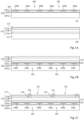
- FIG. 5 is a diagram schematically illustrating the operation of the elementary pixel chip 153 of the figure 4 .
- There figure 5 represents more particularly the evolution, as a function of time, of the signals SELECT, RESET, DATA, VX, as well as of the potential SN of the gate node of the transistor SF, and of the signals MEM(R), MEM(G) and MEM( B) contained respectively in the memories MEM of the control sub-circuits R, G and B.
- the respective transmission setpoint signals DATA R, DATA G and DATA B of the LEDs LR, LG and LB are time multiplexed digital signals on the terminal P2 (signal DATA).
- a transmission data bit of the signal DATA is transmitted from the terminal P2 to the memory 401 of the control sub-circuit R
- the previous transmission data bit is transmitted from the terminal of Q output of the D flip-flop 403 of the R control sub-circuit to the memory 401 of the G control sub-circuit
- the previous transmit data bit is transmitted from the Q output terminal of the D flip-flop 403 of the sub control circuit G to memory 401 of control sub-circuit B.
- three periods of the signal SELECT are necessary to transmit three setpoint signals respectively to the three control sub-circuits R, G and B of the device.
- the signal RESET makes it possible to control the reset transistor RST of the reading circuit of the detection pixel DET. This makes it possible, on each read, to sample a first value of the signal VX at the end of an integration period during which the reset transistor RST is kept off, then a second value of the signal VX immediately after a reset period of the photodetector D1 during which the reset transistor RST is kept on (the end of the reset period marking the start of a second integration period). The difference between the two read values defines the output value of the pixel. A double-sampled readout is thus achieved.
- FIG. 6 is an electrical circuit diagram of another example of an elementary pixel chip 153 of an interactive display device of the type described above.
- the elementary chip 153 of the figure 6 differs from the elementary chip 153 of the figure 4 essentially in that it does not include terminal P6 for applying the reset signal RESET.
- the gate of transistor RST is connected to the drain of this same transistor.
- the RST transistor is connected as a diode.
- FIG 7 is a diagram schematically illustrating the operation of the elementary pixel chip 153 of the figure 6 .
- There figure 7 represents more particularly the evolution, as a function of time, of the signals SELECT, DATA, VX, as well as of the potential SN of the gate node of the transistor SF, and of the signals MEM(R), MEM(G) and MEM(B) contained respectively in the memories MEM of the control sub-circuits R, G and B.
- the diode configuration of the RST transistor operating in weak inversion regime implies a logarithmic response of the voltage on its source according to the current which crosses its channel, in this case the photo-current generated by the photodiode D1.
- the detection pixel reading circuit DET implements a logarithmic reading of the photo-current generated by the photodetector D1.
- transistor RD is turned on.
- the signal VX provided on the output terminal P1 is then an analog voltage representative of the instantaneous luminosity received by the photodetector D1 of the pixel.
- the VX signal can be read and digitized at the bottom of the column.
- the signal VX of the pixel can be read successively three times and an average of the three values can be made, so as to minimize read noise.
- embodiments described are not limited to the particular examples of embodiment of the electronic control circuits (control of the emission of LED light or of the actuation element or reading of the capture or dimmer element). actuation) of the elementary pixel chips described in relation to the figures 4 to 7 .
- the embodiments described are not limited to the particular case described above in which the LEDs of the device are organic LEDs.
- the organic LEDs of the device described can be replaced by inorganic LEDs, for example based on type III-V semiconductor materials, for example based on gallium nitride.
- the LEDs can be replaced, all or in part, by any other capture or actuation element external to the chips 153.
- These capture elements or action can be of any type.
- a non-limiting example of such elements can be, for example, ultrasonic or acoustic transducers, for example of the piezoelectric type. This makes it possible, for example, to implement functions for detecting the touch or proximity of an object, for example the hand of a user, for example by using the direct piezoelectric effect, and/or haptic stimulation functions, and/or directional acoustic wave emission functions, for example by using the indirect piezoelectric effect.
- actuation function is meant, for example, the actuation of piezoelectric actuators in order to generate an ultrasonic wave or a mode of vibration capable of causing a haptic effect sensitive to the user.
- the application of an electric field between the upper electrode and the lower electrode induces a deformation of the piezoelectric material.
- the actuator Depending on the signal sent, for example sinusoidal at a frequency defined as being the dimensioned working frequency, the actuator generates an ultrasonic wave or a vibration mode (for example type of bending mode, or an antisymmetrical Lamb mode), by example capable of generating a haptic effect.
- a vibration mode for example type of bending mode, or an antisymmetrical Lamb mode
- the electronic control circuits of the elementary chips 153 are then replaced by electronic control circuits of the capture or actuation elements, for example control circuits of the ultrasonic transducers in transmission and/or in reception.
- the capture or action elements external to the chips 153 can be photodetectors of a different nature from the photodetectors D1, for example organic photodetectors.
- the electronic control circuits of the elementary chips 153 then include circuits for reading the external photodetectors.
Abstract
La présente description concerne un dispositif comportant :- un substrat de report (200) comportant des éléments de connexion électrique ; et- une pluralité de puces élémentaires (153) fixées et connectées électriquement au substrat de report (200), chaque puce élémentaire (153) comportant au moins un photodétecteur et un circuit électronique de lecture dudit au moins un photodétecteur,- le dispositif comportant en outre, associé à au moins une puce élémentaire (153), un élément (LR, LG, LB) d'émission, de capture ou d'actuation externe à la puce élémentaire (153), fixé et connecté électriquement au substrat de report (200), chaque puce élémentaire (153) comportant un circuit électronique de contrôle de l'élément (LR, LG, LB) d'émission, de capture ou d'actuation associé à la puce.The present description relates to a device comprising:- a transfer substrate (200) comprising electrical connection elements; and- a plurality of elementary chips (153) fixed and electrically connected to the transfer substrate (200), each elementary chip (153) comprising at least one photodetector and an electronic circuit for reading said at least one photodetector,- the device comprising Furthermore, associated with at least one elementary chip (153), an emission, capture or actuation element (LR, LG, LB) external to the elementary chip (153), fixed and electrically connected to the transfer substrate ( 200), each elementary chip (153) comprising an electronic circuit for controlling the emission, capture or actuation element (LR, LG, LB) associated with the chip.
Description
La présente description concerne de façon générale le domaine des dispositifs de capture d'images, et vise plus particulièrement un dispositif de capture d'images dit mixte, combinant une fonction de capture optique et une fonction d'émission lumineuse, et un procédé de fabrication d'un tel dispositif. Plus généralement, elle concerne un dispositif de capture d'images mixte combinant une fonction de capture optique et une autre fonction, par exemple une fonction d'émission ou d'actuation ou une autre fonction de capture.The present description generally relates to the field of image capture devices, and more particularly aims at a so-called mixed image capture device, combining an optical capture function and a light emission function, and a method of manufacturing of such a device. More generally, it relates to a mixed image capture device combining an optical capture function and another function, for example a transmission or actuation function or another capture function.
Il a déjà été proposé, par exemple dans les demandes de brevet
Ce type de dispositif d'affichage est particulièrement adapté pour réaliser des écrans d'affichage de grande surface, par exemple des écrans d'ordinateur, de téléviseur, de tablette, etc.This type of display device is particularly suitable for producing large-area display screens, for example computer screens, television screens, tablets, etc.
On s'intéresse ici plus particulièrement à la réalisation d'un dispositif d'affichage d'images interactif, combinant une fonction d'émission lumineuse et une fonction de capture optique. Plus généralement, on s'intéresse ici à la réalisation d'un dispositif de capture d'images mixte, combinant une fonction de capture optique et une autre fonction, par exemple une fonction d'émission lumineuse ou d'actuation, ou une autre fonction de capture optique.We are more particularly interested here in the production of an interactive image display device, combining a light emission function and an optical capture function. More generally, we are interested here in the production of a mixed image capture device, combining an optical capture function and another function, for example a light emission or actuation function, or another function optical capture.
Un mode de réalisation prévoit un dispositif comportant :
- un substrat de report comportant des éléments de connexion électrique ; et
- une pluralité de puces élémentaires fixées et connectées électriquement au substrat de report, chaque puce élémentaire comportant au moins un photodétecteur et un circuit électronique de lecture dudit au moins un photodétecteur,
le dispositif comportant en outre, associé à au moins une puce élémentaire, un élément d'émission, de capture ou d'actuation externe à la puce élémentaire, fixé et connecté électriquement au substrat de report, chaque puce élémentaire comportant un circuit électronique de contrôle de l'élément d'émission, de capture ou d'actuation associé à la puce.
- a transfer substrate comprising electrical connection elements; And
- a plurality of elementary chips fixed and electrically connected to the transfer substrate, each elementary chip comprising at least one photodetector and an electronic circuit for reading said at least one photodetector,
the device further comprising, associated with at least one elementary chip, an emission, capture or actuation element external to the elementary chip, fixed and electrically connected to the transfer substrate, each elementary chip comprising an electronic control circuit of the emission, capture or actuation element associated with the chip.
Selon un mode de réalisation, dans chaque puce élémentaire, le circuit électronique de lecture dudit au moins un photodétecteur et le circuit électronique de contrôle de l'élément d'émission, de capture ou d'actuation associé à la puce comprennent des transistors MOS formés dans et sur une couche de silicium monocristallin.According to one embodiment, in each elementary chip, the electronic circuit for reading said at least one photodetector and the electronic circuit for controlling the emission, capture or actuation element associated with the chip comprise MOS transistors formed in and on a layer of monocrystalline silicon.
Selon un mode de réalisation, dans chaque puce élémentaire, ledit au moins un photodétecteur est un photodétecteur inorganique à base d'un matériau semiconducteur III-V.According to one embodiment, in each elementary chip, said at least one photodetector is an inorganic photodetector based on a III-V semiconductor material.
Selon un mode de réalisation, dans chaque puce élémentaire, ledit au moins un photodétecteur comprend une couche d'absorption en arséniure d'indium gallium.According to one embodiment, in each elementary chip, said at least one photodetector comprises an indium gallium arsenide absorption layer.
Selon un mode de réalisation, l'élément d'émission, de capture ou d'actuation comprend au moins une diode électroluminescente.According to one embodiment, the emission, capture or actuation element comprises at least one light-emitting diode.
Selon un mode de réalisation, ladite au moins une diode électroluminescente est une diode électroluminescente organique.According to one embodiment, said at least one light-emitting diode is an organic light-emitting diode.
Selon un mode de réalisation, chaque élément d'émission, de capture ou d'actuation comprend trois diodes électroluminescentes définissant respectivement trois sous-pixels d'émission, et dans lequel chaque puce élémentaire comprend une pluralité de sous-circuits de commande adaptés à commander individuellement respectivement les trois diodes électroluminescentes.According to one embodiment, each emission, capture or actuation element comprises three light-emitting diodes respectively defining three emission sub-pixels, and in which each elementary chip comprises a plurality of control sub-circuits suitable for controlling individually respectively the three light-emitting diodes.
Selon un mode de réalisation, les trois sous-pixels d'émission sont adaptés à émettre respectivement dans trois gammes de longueurs d'ondes différentes.According to one embodiment, the three transmission sub-pixels are suitable for transmitting respectively in three different wavelength ranges.
Selon un mode de réalisation, dans chaque puce élémentaire, les trois sous-circuits de commande sont reliés à une même borne d'entrée de la puce, connectée à une plage de connexion correspondante du substrat de report, destinée à recevoir séquentiellement des signaux de consigne d'émission des trois diodes électroluminescentes.According to one embodiment, in each elementary chip, the three control sub-circuits are linked to the same input terminal of the chip, connected to a range corresponding connection of the transfer substrate, intended to sequentially receive transmission setpoint signals from the three light-emitting diodes.
Selon un mode de réalisation, l'élément de capture ou d'actuation associé à chaque puce élémentaire est un transducteur piézoélectrique.According to one embodiment, the capture or actuation element associated with each elementary chip is a piezoelectric transducer.
Ces caractéristiques et avantages, ainsi que d'autres, seront exposés en détail dans la description suivante de modes de réalisation particuliers faite à titre non limitatif en relation avec les figures jointes parmi lesquelles :
- les
figures 1A, 1B, 1C ,1D, 1E, 1F ,1G, 1H, 1I et 1J sont des vues en coupe illustrant des étapes successives d'un exemple d'un procédé de fabrication de puces élémentaires de pixel d'un dispositif de capture d'images mixte selon un mode de réalisation ; - la
figure 2 est une vue de dessus illustrant de façon schématique et partielle un exemple d'un substrat de report d'un dispositif de capture d'images mixte selon un mode de réalisation ; - les
figures 3A, 3B ,3C et 3D sont des vues en coupe illustrant des étapes successives d'un exemple d'un procédé de fabrication d'un dispositif de capture d'images mixte selon un mode de réalisation ; - la
figure 4 est un schéma électrique des circuits d'un exemple d'une puce élémentaire de pixel d'un dispositif de capture d'images mixte selon un mode de réalisation ; - la
figure 5 est un diagramme illustrant de façon schématique le fonctionnement de la puce élémentaire de pixel de lafigure 4 ; - la
figure 6 est un schéma électrique des circuits d'un autre exemple d'une puce élémentaire de pixel d'un dispositif de capture d'images mixte selon un mode de réalisation ; et - la
figure 7 est un diagramme illustrant de façon schématique le fonctionnement de la puce élémentaire de pixel de lafigure 6 .
- THE
Figures 1A, 1B, 1C ,1D, 1E, 1F ,1G, 1H, 1I and 1J are cross-sectional views illustrating successive steps of an example of a method for manufacturing elementary pixel chips of a mixed image capture device according to one embodiment; - there
figure 2 is a top view schematically and partially illustrating an example of a transfer substrate of a mixed image capture device according to one embodiment; - THE
Figures 3A, 3B ,3C and 3D are cross-sectional views illustrating successive steps of an example of a method of manufacturing a mixed image capture device according to one embodiment; - there
figure 4 is an electrical diagram of the circuits of an example of an elementary pixel chip of a mixed image capture device according to one embodiment; - there
figure 5 is a diagram schematically illustrating the operation of the elementary pixel chip of thefigure 4 ; - there
figure 6 is an electric diagram of the circuits of another example of an elementary pixel chip of a mixed image capture device according to one embodiment; And - there
figure 7 is a diagram schematically illustrating the operation of the elementary pixel chip of thefigure 6 .
De mêmes éléments ont été désignés par de mêmes références dans les différentes figures. En particulier, les éléments structurels et/ou fonctionnels communs aux différents modes de réalisation peuvent présenter les mêmes références et peuvent disposer de propriétés structurelles, dimensionnelles et matérielles identiques.The same elements have been designated by the same references in the different figures. In particular, the structural and/or functional elements common to the various embodiments may have the same references and may have identical structural, dimensional and material properties.
Par souci de clarté, seuls les étapes et éléments utiles à la compréhension des modes de réalisation décrits ont été représentés et sont détaillés. En particulier, les diverses applications que peuvent avoir les dispositifs de capture d'images mixtes décrits n'ont pas été détaillées, les modes de réalisation décrits étant compatibles avec toutes ou la plupart des applications connues d'un dispositif de capture optique intégrant une fonction d'affichage émissif, par exemple des applications de détection de mouvement, de reconnaissance de visage, d'identification, etc., et plus généralement, d'un dispositif de capture optique intégrant une autre fonction, par exemple d'émission, de capture ou d'actuation.For the sake of clarity, only the steps and elements useful for understanding the embodiments described have been represented and are detailed. In particular, the various applications that the mixed image capture devices described may have have not been detailed, the embodiments described being compatible with all or most of the known applications of an optical capture device integrating a function emissive display, for example applications for motion detection, face recognition, identification, etc., and more generally, an optical capture device integrating another function, for example transmission, capture or action.
Sauf précision contraire, lorsque l'on fait référence à deux éléments connectés entre eux, cela signifie directement connectés sans éléments intermédiaires autres que des conducteurs, et lorsque l'on fait référence à deux éléments reliés (en anglais "coupled") entre eux, cela signifie que ces deux éléments peuvent être connectés ou être reliés par l'intermédiaire d'un ou plusieurs autres éléments.Unless otherwise specified, when reference is made to two elements connected together, this means directly connected without intermediate elements other than conductors, and when reference is made to two elements connected (in English "coupled") between them, it means that these two elements can be connected or be linked via one or more other elements.
Dans la description qui suit, lorsque l'on fait référence à des qualificatifs de position absolue, tels que les termes "avant", "arrière", "haut", "bas", "gauche", "droite", etc., ou relative, tels que les termes "dessus", "dessous", "supérieur", "inférieur", etc., ou à des qualificatifs d'orientation, tels que les termes "horizontal", "vertical", etc., il est fait référence sauf précision contraire à l'orientation des figures.In the following description, when referring to absolute position qualifiers, such as "front", "rear", "up", "down", "left", "right", etc., or relative, such as the terms "above", "below", "upper", "lower", etc., or to qualifiers of orientation, such as the terms "horizontal", "vertical", etc., it reference is made unless otherwise specified to the orientation of the figures.
Sauf précision contraire, les expressions "environ", "approximativement", "sensiblement", et "de l'ordre de" signifient à 10 % près, de préférence à 5 % près.Unless specified otherwise, the expressions “about”, “approximately”, “substantially”, and “of the order of” mean to within 10%, preferably within 5%.
Selon un aspect d'un mode de réalisation, on prévoit un dispositif de capture d'images comportant une pluralité de puces électroniques monolithiques élémentaires disposées en matrice sur un même substrat de report. Comme dans les exemples décrits dans les demandes de brevet
Selon un aspect d'un mode de réalisation, le dispositif de capture d'images mixte comprend en outre une fonction d'émission de lumière, par exemple une fonction d'affichage d'images. Pour cela, le dispositif comprend une pluralité de diodes électroluminescentes (LED), par exemple des LED organiques, agencées en matrice selon des rangées et des colonnes et définissant un dispositif d'affichage d'images. Les LED sont externes aux puces élémentaires de pixel du dispositif de capture mixte, et sont disposées sur le substrat de report du dispositif, du même côté du substrat de report que les puces élémentaires de pixel. Les LED sont connectées à des bornes de connexion électrique du substrat de report pour leur commande. Les LED peuvent émettre dans le visible ou dans l'infrarouges, voire simultanément dans le visible et dans l'infrarouge auquel cas l'une des émissions (de préférence, l'infrarouge) est captée par le dispositif de capture.According to one aspect of an embodiment, the mixed image capture device further comprises a light emission function, for example an image display function. For this, the device comprises a plurality of light-emitting diodes (LEDs), for example organic LEDs, arranged in a matrix according to rows and columns and defining an image display device. The LEDs are external to the elementary pixel chips of the mixed capture device, and are arranged on the transfer substrate of the device, on the same side of the transfer substrate as the elementary pixel chips. The LEDs are connected to electrical connection terminals of the transfer substrate for their control. The LEDs can emit in the visible or in the infrared, or even simultaneously in the visible and in the infrared, in which case one of the emissions (preferably infrared) is picked up by the capture device.
A titre d'exemple, le dispositif comprend un groupe élémentaire d'une ou plusieurs LED par puce élémentaire de pixel du dispositif de capture mixte, disposé au voisinage de ladite puce élémentaire de pixel. Autrement dit, la matrice de puces élémentaires de pixel du dispositif de capture et la matrice de groupes élémentaires de LED sont des matrices entrelacées de mêmes dimensions et de même pas.By way of example, the device comprises an elementary group of one or more LEDs per elementary pixel chip of the mixed capture device, arranged in the vicinity of said elementary pixel chip. In other words, the matrix of elementary pixel chips of the capture device and the matrix of elementary groups of LEDs are interleaved matrices of the same dimensions and the same pitch.
Selon un aspect d'un mode de réalisation, chaque puce élémentaire de pixel du dispositif de capture mixte intègre un circuit électronique de contrôle du groupe élémentaire d'une ou plusieurs LED correspondant, c'est-à-dire de même position (mêmes coordonnées) dans la matrice de pixels. Chaque puce élémentaire de pixel du dispositif comprend, pour chaque LED du groupe élémentaire d'une ou plusieurs LED correspondant, une borne de connexion connectée individuellement à une électrode de la LED par l'intermédiaire d'une piste conductrice du substrat de report.According to one aspect of an embodiment, each elementary pixel chip of the mixed capture device integrates an electronic circuit for controlling the elementary group of one or more corresponding LEDs, that is to say of the same position (same coordinates) in the matrix of pixels. Each elementary pixel chip of the device comprises, for each LED of the elementary group of one or more corresponding LEDs, a connection terminal individually connected to an electrode of the LED via a conductive track of the transfer substrate.
Des exemples de réalisation d'un tel dispositif de capture d'images mixte vont être décrits plus en détail ci-après en relation avec les figures.Examples of embodiments of such a mixed image capture device will be described in more detail below in relation to the figures.
Les
La
Dans l'exemple représenté, le substrat 101 est un substrat de type SOI (de l'anglais "Semiconductor On Insulator" - semiconducteur sur isolant), comportant un substrat semiconducteur de support 101a, par exemple en silicium, une couche isolante 101b, par exemple en oxyde de silicium, disposée sur et en contact avec la face supérieure du substrat de support 101a, et une couche semiconductrice supérieure 101c, par exemple en silicium monocristallin, disposée sur et en contact avec la face supérieure de la couche isolante 101b.In the example represented, the
Dans cet exemple, les circuits élémentaires de contrôle 103 sont formés dans et sur la couche semiconductrice supérieure 101c du substrat 101. Chaque circuit élémentaire de contrôle 103 comprend par exemple une pluralité de transistors MOS (non détaillés sur les
Dans cet exemple, chaque circuit élémentaire de contrôle 103 comprend, du côté de sa face supérieure, un ou plusieurs plots de connexion métalliques 105a, 105b. A titre d'exemple, les plots 105a, 105b affleurent du côté de la face supérieure d'une couche isolante supérieure, par exemple en oxyde de silicium, d'un empilement d'interconnexion (non détaillé sur les figures) revêtant la face supérieure de la couche semiconductrice supérieure 103c du substrat 101. Ainsi, dans cet exemple, la surface supérieure de la structure de contrôle est une surface plane comportant une alternance de régions métalliques (les plots 105a, 105b) et de régions isolantes.In this example, each
A titre d'exemple, chaque circuit élémentaire de contrôle 103 comprend un plot métallique 105a spécifique pour chaque photodétecteur de la future puce élémentaire de pixel du dispositif, destiné à être connecté à une première borne, par exemple une borne d'anode, du photodétecteur, permettant de lire individuellement un signal électrique représentatif d'un rayonnement lumineux reçu par chaque photodétecteur. Chaque circuit élémentaire de contrôle 103 peut en outre comprendre un plot métallique 105b destiné à être connecté à une deuxième borne, par exemple une borne de cathode de chaque photodétecteur de la future puce élémentaire de pixel du dispositif. Dans le cas où la puce élémentaire comporte plusieurs photodétecteurs, le contact de cathode peut être commun à tous les photodétecteurs de la puce. Ainsi, le circuit élémentaire de contrôle 103 peut comprendre un unique plot métallique 105b. A titre de variante, le circuit élémentaire de contrôle 103 comprend un plot métallique 105b spécifique par photodétecteur.By way of example, each
Dans l'exemple représenté, chaque puce élémentaire de pixel du dispositif comprend un unique photodétecteur, par exemple adapté à capter majoritairement de la lumière infrarouge. Ainsi, chaque circuit élémentaire de contrôle 103 comprend un unique plot métallique 105a et un unique plot métallique 105b destinés à être connectés respectivement aux régions d'anode et de cathode du photodétecteur.In the example represented, each elementary pixel chip of the device comprises a single photodetector, for example adapted to mainly capture infrared light. Thus, each
La
L'empilement 113 est un empilement de couches semiconductrices inorganiques. L'empilement 113 comprend par exemple une ou plusieurs couches en un matériau semiconducteur de type III-V. L'empilement 113 est par exemple un empilement actif de photodiode sensible dans l'infrarouge ou le proche infrarouge. A titre de variante, l'empilement 113 est un empilement actif de photodiode sensible dans le visible. A titre d'exemple, l'empilement 113 comprend, dans l'ordre à partir de la face supérieure du substrat 111, une couche 113a en phosphure d'indium (InP) non intentionnellement dopé, une couche d'absorption 113b en arséniure d'indium-gallium (InGaAs), par exemple intrinsèque ou faiblement dopé de type N (par exemple de l'ordre de 1015 atomes/cm3), et une couche 113c en phosphure d'indium (InP) dopé de type N. A titre d'exemple, le niveau de dopage de type N de la couche 113c est compris entre 1016 et 1018 atomes/cm3. Dans cet exemple, la couche 113b est en contact, par sa face inférieure, avec la face supérieure de la couche 113a, et la couche 113c est en contact, par sa face inférieure, avec la face supérieure de la couche 113b.
Le substrat 111 est par exemple en phosphure d'indium. Les couches 113a, 113b et 113c peuvent être formées successivement par épitaxie sur la face supérieure du substrat 111. Le substrat 111 est alors un substrat de croissance. Une couche tampon, non représentée, par exemple en phosphure d'indium, peut éventuellement faire interface entre le substrat 111 et la couche 113a. La couche tampon est par exemple en contact, par sa face inférieure, avec la face supérieure du substrat 111, et, par sa face supérieure, avec la face inférieure de la couche 113a. La couche tampon peut également être formée par épitaxie à partir de la face supérieure du substrat 111, avant la formation des couches 113a, 113b et 113c.The
A titre de variante, plutôt que de former l'empilement actif de diode photosensible 113 par épitaxie sur la face supérieure du substrat 111, l'empilement actif peut être formé dans l'ordre inverse sur un substrat de croissance, non représenté, puis reporté et fixé sur le substrat 111. Dans ce cas, les couches 113c, 113b et 113a sont successivement formées par épitaxie sur une face du substrat de croissance. Une couche tampon, par exemple en phosphure d'indium, peut éventuellement faire interface entre le substrat de croissance et la couche 113c. L'empilement 113 est ensuite fixé sur la face supérieure du substrat 111, par exemple par collage direct ou collage moléculaire de la face inférieure de la couche 113a sur la face supérieure du substrat 111. Le substrat de croissance, et, le cas échéant, la couche tampon faisant interface entre le substrat de croissance et la couche 113c, peuvent ensuite être retirés de façon à libérer l'accès à la face supérieure de la couche 113c. Dans cette variante, le substrat 111 est un substrat de support, par exemple en silicium, ou en tout autre matériau adapté à servir de support de réception de l'empilement actif 113.As a variant, rather than forming the active
A ce stade, chacune des couches de l'empilement actif de diode photosensible 113 s'étend par exemple de façon continue et avec une épaisseur sensiblement uniforme sur toute la surface supérieure du substrat 111.At this stage, each of the layers of the active
La
La
La
Sur la
Lors de cette étape, la structure de la vue (b) de la
Le substrat 111 est ensuite retiré, par exemple par meulage et/ou gravure chimique, de façon à libérer l'accès à la face supérieure de l'empilement actif de diode photosensible 113, c'est-à-dire, dans cet exemple, la face supérieure de la couche semiconductrice 113a.The
La
- i) dépôt d'une couche diélectrique 117, par exemple en nitrure de silicium ou en oxyde de silicium, sur la face supérieure de la couche 113a, par exemple en contact avec la face supérieure de la couche 113a ;
- ii) formation d'ouvertures traversantes localisées dans la couche diélectrique 117, en vis-à-vis de futures zones de reprise de contact de type P correspondant à des régions d'anode des diodes photosensibles du dispositif ;
- iii) dopage de type P de régions localisées 119 de la couche 113a, situées en vis-à-vis desdites ouvertures traversantes ;
- iv) formation de métallisations de reprise de contact 121 dans les ouvertures traversantes, chaque métallisation 121 venant contacter individuellement la région dopée de
type P 119 sous-jacente, à travers l'ouverture correspondante.
- i) depositing a
dielectric layer 117, for example of silicon nitride or silicon oxide, on the upper face of thelayer 113a, for example in contact with the upper face of thelayer 113a; - ii) formation of through openings located in
dielectric layer 117, facing future P-type contact recovery zones corresponding to anode regions of the photosensitive diodes of the device; - iii) P-type doping of
localized regions 119 of thelayer 113a, located opposite said through openings; - iv) formation of
contact recovery metallizations 121 in the through openings, eachmetallization 121 individually coming into contact with the underlying P-type dopedregion 119, through the corresponding opening.
A l'étape i), la couche diélectrique 117 est par exemple déposée par un procédé de dépôt chimique en phase vapeur assisté par plasma (PECVD).In step i), the
A l'étape ii), les ouvertures traversantes formées dans la couche diélectrique 117 sont par exemple formées par photolithographie et gravure.In step ii), the through openings formed in the
A l'étape iii), le dopage des régions 119 peut être réalisé par diffusion ou implantation d'éléments dopants de type P, par exemple du zinc (Zn) ou du béryllium (Be), en vis-à-vis des ouvertures formées à l'étape ii). Un recuit d'activation des éléments dopants peut ensuite être mis en oeuvre. A titre d'exemple, le recuit d'activation peut être un recuit laser superficiel, ce qui permet de ne pas altérer les circuits intégrés 103 ni la qualité du collage entre les circuits intégrés 103 et l'empilement actif de diode photosensible 113. Les régions dopées de type P 119 forment des régions d'anode des diodes photosensibles du dispositif. Dans cet exemple, les régions 119 s'étendent sur toute l'épaisseur de la couche 113a, et viennent en contact, par leur face inférieure, avec la face supérieure de la couche d'absorption 113b.In step iii), the doping of the
A l'étape iv), à titre d'exemple, une couche métallique est d'abord déposée de façon continue sur toute la surface supérieure de la structure, c'est-à-dire sur et en contact avec la face supérieure de la couche diélectrique 117 et dans les ouvertures formées à l'étape ii), puis retirée par photolithographie et gravure en conservant les métallisations 121. Dans cet exemple, chaque métallisation 121 constitue une électrode d'anode d'une diode photosensible D1 du dispositif.In step iv), by way of example, a metal layer is first deposited continuously over the entire upper surface of the structure, that is to say on and in contact with the upper face of the
La
La
La
La
La
Dans cet exemple, les vias 131 de reprise de contact d'anode des diodes D1 sont isolés des couches de l'empilement 113 par la couche d'isolation latérale 125. Les vias 133 de reprise de contact de cathode des diodes D1 sont isolés de la couche 113a par la couche d'isolation latérale 129 et sont en contact, latéralement, avec la couche de cathode 113c. Les vias 133 connectent électriquement la couche de cathode 113c de l'empilement de diode photosensible aux plots 105b de connexion de cathode des diodes photosensibles D1. A titre de variante, la couche d'isolation latérale supérieure 129 peut être omise. En effet, dans la mesure les couches 113b et 113a de l'empilement 113 sont peu ou pas dopées, le contact latéral entre le via 133 et lesdites couches 113b, 113c n'entraine pas de court-circuit des diodes D1.In this example, the anode contact recovery vias 131 of the diodes D1 are isolated from the layers of the
La
A cette étape, on forme par exemple, pour chaque diode D1, une métallisation 135 connectant électriquement le via de reprise de contact d'anode 131 de la diode D1 à la métallisation de contact d'anode 121 de cette diode.At this step, for example, for each diode D1, a
A titre d'exemple, une couche de métal est d'abord déposée pleine plaque sur toute la surface supérieure de la structure de la
La
La
La
On notera que les modes de réalisation décrits ne se limitent pas à l'exemple décrit ci-dessus dans lequel le substrat 101 est un substrat de type SOI. A titre de variante, le substrat 101 peut être un substrat semiconducteur massif, par exemple en silicium. Dans ce cas, à l'étape de la
La
Les métallisations 143 forment des bornes de connexion des futures puces élémentaires de pixel du dispositif, destinées à être connectées à des bornes de connexion correspondantes du substrat de report du dispositif.The
La
A titre de variante, non représentée, des étapes de formation de filtres optiques peuvent être prévues, par exemple après le dépôt de la couche de passivation 137 et avant la fixation du substrat de support temporaire 140. Ainsi, chaque diode photosensible D1 peut être revêtue, du côté de sa face d'exposition à la lumière, à savoir sa face inférieure dans l'orientation de la
Les puces élémentaires de pixel 153 sont destinées à être reportées sur un substrat de report 200 du dispositif de capture, comme cela sera décrit plus en détail ci-après en relation avec les
La
Sur la
Le substrat de report 200 comprend par exemple une plaque ou feuille de support 201 en un matériau isolant, par exemple en verre ou en plastique. A titre de variante, la plaque ou feuille de support 201 comprend un support conducteur, par exemple métallique, recouvert par une couche d'un matériau isolant. Le substrat de report comprend en outre des éléments de connexion électrique, et en particulier des pistes conductrices et des plages conductrices, formés sur la face supérieure de la plaque de support 201. Ces éléments de connexion électrique sont par exemple formés par impression d'une succession de niveaux conducteurs et isolants sur la face supérieure de la plaque de support 201. Les éléments de connexion électrique sont par exemple formés par un procédé de dépôt ou d'impression de type impression jet d'encre, par sérigraphie, par rotogravure, par dépôt sous vide, ou par toute autre méthode adaptée.The
Dans l'exemple représenté, le substrat de report 201 comprend deux niveaux métalliques conducteurs M1 et M2 séparés par un niveau isolant (non visible sur la figure), et des vias métalliques V connectant les deux niveaux métalliques à travers le niveau isolant. Dans cet exemple, le substrat de report 201 comprend en outre des plages métalliques de connexion formées sur le niveau métallique supérieur M2, destinées à être connectées à des plages de connexion 143 correspondantes des puces élémentaires de pixel 153 du dispositif.In the example represented, the
Des circuits actifs de commande du dispositif d'affichage, adaptés à alimenter et commander les puces élémentaires du dispositif par l'intermédiaire des éléments de connexion électrique du substrat de report, sont par exemple connectés aux éléments de connexion électrique du substrat de report à la périphérie du substrat de report 200.Active circuits for controlling the display device, suitable for powering and controlling the elementary chips of the device via the electrical connection elements of the transfer substrate, are for example connected to the electrical connection elements of the transfer substrate at the periphery of
Dans l'exemple représenté, la fabrication du substrat de report comprend les trois étapes successives de dépôt suivantes.In the example shown, the manufacture of the transfer substrate comprises the following three successive deposition steps.
Lors d'une première étape de dépôt, on forme sur la face supérieure de la plaque de support 201 une pluralité de pistes conductrices sensiblement parallèles à la direction des colonnes du dispositif d'affichage (direction verticale dans l'orientation de la
Les éléments conducteurs formés lors de cette première étape de dépôt définissent le premier niveau conducteur M1 du substrat de report.The conductive elements formed during this first deposition step define the first conductive level M1 of the transfer substrate.
Lors d'une deuxième étape de dépôt, on recouvre le premier conducteur d'un matériau isolant (non visible sur la figure), de façon à permettre le dépôt ultérieur de pistes conductrices s'étendant au-dessus des pistes C1, C2 et C3, sans créer de court-circuit avec les pistes C1, C2 et C3.During a second deposition step, the first conductor is covered with an insulating material (not visible in the figure), so as to allow the subsequent deposition of conductive tracks extending above the tracks C1, C2 and C3 , without creating a short-circuit with tracks C1, C2 and C3.
Lors d'une troisième étape de dépôt, on forme sur la face supérieure de la plaque de support 201, une pluralité de pistes conductrices sensiblement parallèles à la direction des lignes du dispositif d'affichage. Plus particulièrement, dans cet exemple, lors de la troisième étape de dépôt, on imprime, pour chaque ligne du dispositif d'affichage, trois pistes conductrices L1, L2 et L3 s'étendant sur sensiblement toute la longueur des lignes du dispositif d'affichage. Les pistes L1 sont destinées à véhiculer un signal RESET de commande de réinitialisation des photodétecteurs de la ligne de pixel correspondante. Les pistes L2 sont destinées à véhiculer un signal SELECT de sélection des photodétecteurs et/ou des LED de la ligne de pixel correspondante. Les pistes L3 sont destinées à distribuer un potentiel de polarisation fixe VA, par exemple inférieur au potentiel VDD, aux différentes puces élémentaires de pixel 153.During a third deposition step, a plurality of conductive tracks are formed on the upper face of
Dans cet exemple, le dispositif que l'on cherche à réaliser comprend, pour chaque puce élémentaire de pixel 153, trois LED organiques LR, LG, LB définissant respectivement un sous-pixel d'émission de lumière rouge, un sous-pixel d'émission de lumière verte et un sous-pixel d'émission de lumière bleue du dispositif.In this example, the device that is sought to be produced comprises, for each
Dans cet exemple, lors de la troisième étape de dépôt, sont en outre imprimées, pour chaque pixel du dispositif, trois régions métalliques AR, AG, AB, définissant les électrodes d'anode respectives des LED organiques LR, LG, LB du pixel. De plus, dans cet exemple, lors de la troisième étape de dépôt, est en outre imprimée, pour chaque pixel du dispositif, une région métallique K définissant une plage de reprise de contact de cathode commune aux LED organiques LR, LG, LB du pixel.In this example, during the third deposition step, are additionally printed, for each pixel of the device, three metal regions AR, AG, AB, defining the respective anode electrodes of the organic LEDs LR, LG, LB of the pixel. Moreover, in this example, during the third deposition step, is additionally printed, for each pixel of the device, a metallic region K defining a cathode contact recovery area common to the organic LEDs LR, LG, LB of the pixel .
Les éléments conducteurs imprimés lors de cette troisième étape de dépôt définissent le deuxième niveau conducteur M2 du substrat de report.The conductive elements printed during this third deposition step define the second conductive level M2 of the transfer substrate.
Après la troisième étape de dépôt, on vient former, pour chaque pixel, sur des zones conductrices du niveau métallique M2, dix plages métalliques P1, P2, P3, P4, P5, P6, P7, P8, P9 et P10 destinées à recevoir respectivement dix plages de connexion 143 distinctes de la puce élémentaire 153 du pixel. Les plages P1, P2, P3 sont connectées respectivement aux pistes conductrices C1, C2 et C3 de la colonne de pixels correspondante. Les plages P4 et P5 sont connectées respectivement aux électrodes AR et AG du pixel. Les plages P6, P7, P8 sont connectées respectivement aux pistes conductrices L1, L2, L3 de la ligne de pixels correspondante. Les plages P9 et P10 sont connectées respectivement aux électrodes K et AB du pixel.After the third deposition step, ten metal pads P1, P2, P3, P4, P5, P6, P7, P8, P9 and P10 intended to receive respectively ten
Les vias V reliant les niveaux métalliques inférieur M1 et supérieur M2 sont ouverts dans le niveau isolant séparant les niveaux M1 et M2, avant la formation du niveau supérieur M2.The vias V connecting the lower M1 and upper M2 metallic levels are open in the insulating level separating the levels M1 and M2, before the formation of the upper level M2.
Les
Par souci de simplification, sur les
Les
La
La
Les couches actives 211-R, 211-G, 211-B sont déposées successivement, de façon localisée, respectivement sur les électrodes AR, AG, AB de chaque pixel, par exemple par évaporation au travers d'un pochoir ("shadow mask" en anglais). A titre de variante, les couches actives 211-R, 211-G, 211-B sont déposées successivement par un procédé d'impression localisée, par exemple par impression jet d'encre, par sérigraphie ou par un procédé de revêtement par filière à fente ("slot-die coating" en anglais). Dans chaque sous-pixels d'émission, la portion de couche active organique 211-R, 211-G, 211-B du sous-pixel s'étend par exemple sur toute la surface supérieure de l'électrode AR, respectivement AG, respectivement AB correspondante. Les couches actives 211-R, 211-G et 211-B sont par exemple adaptées à émettre majoritairement respectivement de la lumière rouge, de la lumière verte, et de la lumière bleue, et optionnellement un rayonnement infrarouge.The active layers 211-R, 211-G, 211-B are deposited successively, in a localized manner, respectively on the electrodes AR, AG, AB of each pixel, for example by evaporation through a stencil ("shadow mask" in English). As a variant, the active layers 211-R, 211-G, 211-B are successively deposited by a localized printing process, for example by inkjet printing, by screen printing or by a coating process using a die to slot ("slot-die coating" in English). In every sub-pixel emission, the organic active layer portion 211-R, 211-G, 211-B of the sub-pixel extends for example over the entire upper surface of the corresponding electrode AR, respectively AG, respectively AB. The active layers 211-R, 211-G and 211-B are for example adapted to mainly emit respectively red light, green light, and blue light, and optionally infrared radiation.
La couche d'électrode supérieure 213 s'étend de façon continue sur et en contact avec la face supérieure des couches actives 211-R, 211-G, 211-B. La couche d'électrode supérieure 213 s'étend en outre sur et en contact avec la face supérieure de la région métallique de reprise de contact de cathode K commune aux LED LR, LG, LB. La couche d'électrode supérieure 213 est transparente aux longueurs d'onde d'émissions des LED LR, LG, LB. A titre d'exemple, la couche d'électrode supérieure 213 est en un oxyde conducteur transparent, par exemple en oxyde d'indium-étain (ITO). La couche d'électrode supérieure 213 peut être déposée de façon localisée, pour chaque pixel, au-dessus des couches actives 211-R, 211-G, 211-B et de la région métallique K du pixel, par exemple par évaporation au-travers d'un pochoir. En particulier, la couche 213 ne s'étend pas au-dessus des plages métalliques P1, P2, P3, P4, P5, P6, P7, P8, P9, P10 ni au-dessus des pistes conductrices L1, L2, L3, de façon à ne pas court-circuiter ces éléments.
A l'issue de ces étapes, les LED organiques LR, LG, LB sont formées. La LED LR est constituée par l'empilement des couches AR, 211-R et 213. La LED LG est constituée par l'empilement des couches AG, 211-G et 213. La LED LB est constituée par l'empilement des couches AB, 211-B et 213.At the end of these steps, the organic LEDs LR, LG, LB are formed. The LED LR is formed by the stacking of layers AR, 211-R and 213. The LED LG is formed by the stacking of layers AG, 211-G and 213. The LED LB is formed by the stacking of layers AB , 211-B and 213.
Après le dépôt de la couche d'électrode supérieure 213, une couche isolante transparente d'encapsulation, non représentée, est de préférence déposée sur la face supérieure des LED organiques. La couche de protection est par exemple en alumine (Al2O3) ou en oxyde de silicium. Dans cet exemple, la couche d'encapsulation ne recouvre pas les plages métalliques de contact P1, P2, P3, P4, P5, P6, P7, P8, P9, P10, de façon à permettre la connexion ultérieure des puces élémentaires 153 sur ces plages.After the deposition of the
Les
Les puces élémentaires 153 sont initialement fixées à une face du substrat de support temporaire 140. La structure comportant le substrat de support temporaire 140 et les puces élémentaires 153 est par exemple réalisée par un procédé du type décrit en relation avec les
Les puces élémentaires 153 sont rapportées collectivement en vis-à-vis de la face de connexion du substrat de report 200, à savoir sa face supérieure dans l'orientation des
Les bornes de connexion 143 de puces élémentaires 153, situées du côté de la face inférieure desdites puces, sont alors mises en contact avec les plages de connexion correspondantes P1, P2, P3, P4, P5, P6, P7, P8, P9, P10 du substrat de report 200, et fixées auxdites plages de connexion P1, P2, P3, P4, P5, P6, P7, P8, P9, P10. La fixation des bornes de connexion 143 des puces élémentaires 153 aux plages de connexion du substrat de report est par exemple réalisée par collage direct, par thermocompression, par brasure, au moyen de microstructure métalliques (par exemple des micropiliers) préalablement formées sur les bornes 143, ou par toute autre méthode de fixation et de connexion adaptée.The
Une fois fixées, par leurs bornes de connexion 143, au substrat de report 200, les puces élémentaires 153 sont détachées du substrat de support temporaire 140 et ce dernier est retiré (
Le pas des puces élémentaires 153 sur le substrat de report 200 peut être supérieur au pas des micropuces élémentaires 153 sur le substrat de support temporaire 140. De préférence, le pas des puces élémentaires 153 sur le substrat de report 200 est un multiple du pas des micropuces élémentaires 153 sur le substrat de support temporaire 140. Dans ce cas, seule une partie des puces 153 est prélevée sur le substrat de support 140 à chaque transfert, comme illustré sur les
Dans cet exemple, les LED organiques LR, LG, LB sont formées avant le report des puces élémentaires 153 sur le substrat de report 200. A titre de variante, les LED organiques LR, LG, LB peuvent être formées après le report des puces élémentaires 153 sur le substrat 200. Dans ce cas, la couche d'encapsulation des LED organiques peut s'étendre de façon continue sur toute la surface supérieure du dispositif, c'est-à-dire non seulement sur les LED organiques mais aussi sur la face supérieure et sur les flancs des puces élémentaires 153.In this example, the organic LEDs LR, LG, LB are formed before the transfer of the
Des systèmes optiques (par exemple des lentilles de focalisation de l'image captée) peuvent être rajoutées dur les dispositifs de capture.Optical systems (for example lenses for focusing the captured image) can be added to the capture devices.
La
Dans cet exemple, la puce 153 est une puce à 10 bornes ou plots de connexion 143 connectés respectivement aux dix plages de connexion P1, P2, P3, P4, P5, P6, P7, P8, P9 et P10 du substrat de support 200 de la
La puce 153 de la
Dans cet exemple, chacun des sous-circuits de commande R, G et B comprend un transistor MOS SW ayant un premier noeud de conduction relié, par exemple connecté, à la borne P3 d'application du potentiel d'alimentation haut VDD, et un deuxième noeud de conduction relié, par exemple connecté, à la borne d'anode P4, respectivement P5, respectivement P10 de la LED LR, respectivement LG, respectivement LB correspondante. Dans cet exemple, les transistors SW sont des transistors MOS à canal P, chaque transistor SW ayant sa source reliée, par exemple connectée, à la borne P3 et son drain relié, par exemple connecté, à l'anode de la LED 123 du sous-pixel.In this example, each of the control sub-circuits R, G and B comprises a MOS transistor SW having a first conduction node connected, for example connected, to the terminal P3 for applying the high supply potential VDD, and a second conduction node connected, for example connected, to the anode terminal P4, respectively P5, respectively P10 of the corresponding LED LR, respectively LG, respectively LB. In this example, the SW transistors are P-channel MOS transistors, each SW transistor having its source connected, for example connected, to terminal P3 and its drain connected, for example connected, to the anode of the
Les cathodes des LED LR, LG, LB peuvent être connectées à la borne P9 de la puce, fournissant un potentiel de polarisation fixe VK, inférieur au potentiel VDD. La puce 153 peut comprendre un circuit, non détaillé, de fourniture du potentiel VK. En variante, les bornes P8 et P9 peuvent être reliées, le potentiel VK de cathode des LED LR, LG, LB étant alors égal au potentiel VA d'anode de la diode photosensible D1. Dans une autre variante, la borne P9 peut être omise, le potentiel VK étant distribué sur les métallisations K des pixels par l'intermédiaire de pistes conductrices de colonne ou de ligne formées dans le niveau de métallisations M1 ou M2 du substrat de report 200.The cathodes of the LEDs LR, LG, LB can be connected to the terminal P9 of the chip, providing a fixed bias potential VK, lower than the potential VDD.
Dans cet exemple, les LED LR, LG, LB sont commandées au moyen de signaux de consigne numériques à codage binaire, par exemple selon un procédé de commande de type PWM (de l'anglais "Pulse Width Modulation" - modulation en largeur d'impulsion), par exemple du type décrit dans la demande de brevet
Dans cet exemple, le circuit READ de lecture du pixel de détection DET comprend trois transistors MOS à canal N RST, SF et RD. Le transistor RST a son drain relié, par exemple connecté, à la borne P3 d'application du potentiel d'alimentation haut VDD et sa source reliée, par exemple connectée, à la cathode du photodétecteur D1. Dans cet exemple, la grille du transistor RST est connectée à la borne P6 d'application du signal de réinitialisation RESET du pixel. Le transistor SF a son drain relié, par exemple connecté, à la borne P3 et sa source reliée, par exemple connectée, au drain du transistor RD. Le transistor SF a sa grille reliée, par exemple connectée, à la source du transistor RST. Le transistor RD a sa source reliée, par exemple connectée, à la borne P1 de fourniture du signal de sortie VX du photodétecteur. La grille du transistor RD est reliée, par exemple connectée, à la borne P7 d'application du signal de commande SELECT.In this example, the circuit READ for reading the detection pixel DET comprises three N-channel MOS transistors RST, SF and RD. The transistor RST has its drain connected, for example connected, to the terminal P3 for applying the high supply voltage VDD and its source connected, for example connected, to the cathode of the photodetector D1. In this example, the gate of the transistor RST is connected to the terminal P6 of application of the reset signal RESET of the pixel. The transistor SF has its drain connected, for example connected, to the terminal P3 and its source connected, for example connected, to the drain of the transistor RD. The transistor SF has its gate connected, for example connected, to the source of the transistor RST. The transistor RD has its source connected, for example connected, to the terminal P1 supplying the output signal VX of the photodetector. The gate of transistor RD is connected, for example connected, to terminal P7 of application of control signal SELECT.
La
Dans cet exemple, les signaux de consigne d'émission respectifs DATA R, DATA G et DATA B des LED LR, LG et LB sont des signaux numériques multiplexés temporellement sur la borne P2 (signal DATA). A chaque front montant du signal SELECT, un bit de donnée d'émission du signal DATA est transmis de la borne P2 à la mémoire 401 du sous-circuit de commande R, le bit de données d'émission précédent est transmis de la borne de sortie Q de la bascule D 403 du sous-circuit de commande R à la mémoire 401 du sous-circuit de commande G, et le bit de données d'émission précédent est transmis de la borne de sortie Q de la bascule D 403 du sous-circuit de commande G à la mémoire 401 du sous-circuit de commande B. Ainsi, trois périodes du signal SELECT sont nécessaires pour transmettre trois signaux de consigne respectivement aux trois sous-circuits de commande R, G et B du dispositif.In this example, the respective transmission setpoint signals DATA R, DATA G and DATA B of the LEDs LR, LG and LB are time multiplexed digital signals on the terminal P2 (signal DATA). At each rising edge of the signal SELECT, a transmission data bit of the signal DATA is transmitted from the terminal P2 to the
Dans cet exemple, le signal RESET permet de commander le transistor de réinitialisation RST du circuit de lecture du pixel de détection DET. Ceci permet, à chaque lecture, d'échantillonner une première valeur du signal VX à la fin d'une période d'intégration pendant laquelle le transistor de réinitialisation RST est maintenu bloqué, puis une deuxième valeur du signal VX immédiatement après une période de réinitialisation du photodétecteur D1 pendant laquelle le transistor de réinitialisation RST est maintenu passant (la fin de la période de réinitialisation marquant le début d'une deuxième période d'intégration). La différence entre les deux valeurs lues définit la valeur de sortie du pixel. On réalise ainsi une lecture à échantillonnage double.In this example, the signal RESET makes it possible to control the reset transistor RST of the reading circuit of the detection pixel DET. This makes it possible, on each read, to sample a first value of the signal VX at the end of an integration period during which the reset transistor RST is kept off, then a second value of the signal VX immediately after a reset period of the photodetector D1 during which the reset transistor RST is kept on (the end of the reset period marking the start of a second integration period). The difference between the two read values defines the output value of the pixel. A double-sampled readout is thus achieved.
La
La puce élémentaire 153 de la
Dans l'exemple de la
La
La configuration en diode du transistor RST fonctionnant en régime de faible inversion implique une réponse logarithmique de la tension sur sa source en fonction du courant qui traverse son canal, dans ce cas le photo-courant généré par la photodiode D1. Ainsi, le circuit de lecture du pixel de détection DET met en oeuvre une lecture logarithmique du photo-courant généré par le photodétecteur D1. A chaque période d'activation du signal SELECT, le transistor RD est rendu passant. Le signal VX fourni sur la borne de sortie P1 est alors une tension analogique représentative de la luminosité instantanée reçue par le photodétecteur D1 du pixel. Le signal VX peut être lu et numérisé en pied de colonne. A titre d'exemple, à chaque mise à jour des signaux de consigne d'émission des sous-circuit de commande R, G et B de la puce, le signal VX du pixel peut être lu successivement trois fois et une moyenne des trois valeurs peut être réalisée, de façon à minimiser le bruit de lecture.The diode configuration of the RST transistor operating in weak inversion regime implies a logarithmic response of the voltage on its source according to the current which crosses its channel, in this case the photo-current generated by the photodiode D1. Thus, the detection pixel reading circuit DET implements a logarithmic reading of the photo-current generated by the photodetector D1. At each period of activation of signal SELECT, transistor RD is turned on. The signal VX provided on the output terminal P1 is then an analog voltage representative of the instantaneous luminosity received by the photodetector D1 of the pixel. The VX signal can be read and digitized at the bottom of the column. By way of example, on each update of the transmission setpoint signals of the R, G and B control sub-circuits of the chip, the signal VX of the pixel can be read successively three times and an average of the three values can be made, so as to minimize read noise.
Divers modes de réalisation et variantes ont été décrits. La personne du métier comprendra que certaines caractéristiques de ces divers modes de réalisation et variantes pourraient être combinées, et d'autres variantes apparaîtront à la personne du métier. En particulier, les modes de réalisation décrits ne se limitent pas aux exemples particuliers de réalisation des puces élémentaires de pixel et du substrat de report décrits en relation avec les
En outre, les modes de réalisation décrits ne se limitent pas aux exemples particuliers de réalisation des circuits électroniques de contrôle (commande de l'émission de lumière de LED ou de l'élément d'actuation ou lecture de l'élément de capture ou d'actuation) des puces élémentaires de pixel décrits en relation avec les
De plus, les modes de réalisation décrits ne se limitent pas au cas particulier décrit ci-dessus dans lequel les LED du dispositif sont des LED organiques. A titre de variante, les LED organiques du dispositif décrit peuvent être remplacés par des LED inorganiques, par exemple à base de matériaux semiconducteurs de type III-V, par exemple à base de nitrure de gallium.Moreover, the embodiments described are not limited to the particular case described above in which the LEDs of the device are organic LEDs. As a variant, the organic LEDs of the device described can be replaced by inorganic LEDs, for example based on type III-V semiconductor materials, for example based on gallium nitride.
Plus généralement, les LED peuvent être remplacées, toutes ou en partie, par tout autre élément de capture ou d'actuation externes aux puces 153. Ces éléments de capture ou d'actuation peuvent être de tout type. Un exemple non limitatif de tels éléments peut être, par exemple, des transducteurs ultrasonores ou acoustiques, par exemple de type piézoélectrique. Ceci permet par exemple de mettre en oeuvre des fonctions de détection de toucher ou de proximité d'un objet, par exemple la main d'un utilisateur, par exemple en utilisant l'effet piézoélectrique direct, et/ou des fonctions de stimulation haptique, et/ou des fonctions d'émission d'ondes acoustiques directives, par exemple en utilisant l'effet piézoélectrique indirect.More generally, the LEDs can be replaced, all or in part, by any other capture or actuation element external to the
Ainsi, par fonction d'actuation, on entend, par exemple, l'actionnement d'actionneurs piézoélectriques afin de générer une onde ultrasonore ou un mode de vibration apte à provoquer un effet haptique sensible à l'utilisateur.Thus, by actuation function is meant, for example, the actuation of piezoelectric actuators in order to generate an ultrasonic wave or a mode of vibration capable of causing a haptic effect sensitive to the user.
A titre d'exemple, tout ou une partie des photodétecteur peuvent être remplacés par des actionneurs piézoélectriques comprenant chacun un empilement :
- d'une électrode inférieure, par exemple métallique, par exemple en argent, en molybdène, en platine, en or ou en un alliage d'un ou plusieurs de ces matériaux,
- d'une couche d'un matériau piézoélectrique, par exemple du titano-zirconiate de plomb (PZT), du nitrure d'aluminium (AlN), ou tout autre matériau piézoélectrique, et
- d'une électrode supérieure, par exemple métallique, par exemple en argent, en molybdène, en platine, en ruthénium, en or, ou en un alliage d'un ou plusieurs de ces matériaux.
- a lower electrode, for example metallic, for example silver, molybdenum, platinum, gold or an alloy of one or more of these materials,
- a layer of a piezoelectric material, for example lead titano-zirconate (PZT), aluminum nitride (AlN), or any other piezoelectric material, and
- an upper electrode, for example metallic, for example silver, molybdenum, platinum, ruthenium, gold, or an alloy of one or more of these materials.
L'application d'un champ électrique entre l'électrode supérieure et l'électrode inférieure induit une déformation du matériau piézoélectrique. Suivant le signal envoyé, par exemple sinusoïdal à une fréquence définie comme étant la fréquence de travail dimensionnée, l'actionneur génère une onde ultrasonore ou un mode de vibration (par exemple type mode de flexion, ou un mode de Lamb antisymétrique), par exemple apte à générer un effet haptique. Cet effet peut résulter d'une variation du coefficient de friction, notamment si le mode de vibration généré est un mode de Lamb.The application of an electric field between the upper electrode and the lower electrode induces a deformation of the piezoelectric material. Depending on the signal sent, for example sinusoidal at a frequency defined as being the dimensioned working frequency, the actuator generates an ultrasonic wave or a vibration mode (for example type of bending mode, or an antisymmetrical Lamb mode), by example capable of generating a haptic effect. This effect can result from a variation of the coefficient of friction, in particular if the vibration mode generated is a Lamb mode.
Les circuits électroniques de contrôle des puces élémentaires 153 sont alors remplacés par des circuits électroniques de commande des éléments de capture ou d'actuation, par exemple des circuits de commande des transducteurs ultrasonores en émission et/ou en réception.The electronic control circuits of the
A titre de variante, les éléments de capture ou d'action externes aux puces 153 peuvent être des photodétecteurs de nature différente des photodétecteurs D1, par exemple des photodétecteurs organiques. Les circuits électroniques de contrôle des puces élémentaires 153 comprennent alors des circuits de lecture des photodétecteurs externes.As a variant, the capture or action elements external to the
Enfin, la mise en oeuvre pratique des modes de réalisation et variantes décrits est à la portée de la personne du métier à partir des indications fonctionnelles données ci-dessus.Finally, the practical implementation of the embodiments and variants described is within the abilities of those skilled in the art based on the functional indications given above.
Claims (10)
Applications Claiming Priority (1)
| Application Number | Priority Date | Filing Date | Title |
|---|---|---|---|
| FR2108774A FR3126261B1 (en) | 2021-08-19 | 2021-08-19 | Image capture device and method of manufacturing such a device |
Publications (2)
| Publication Number | Publication Date |
|---|---|
| EP4138128A1 true EP4138128A1 (en) | 2023-02-22 |
| EP4138128B1 EP4138128B1 (en) | 2023-12-20 |
Family
ID=78820311
Family Applications (1)
| Application Number | Title | Priority Date | Filing Date |
|---|---|---|---|
| EP22189384.5A Active EP4138128B1 (en) | 2021-08-19 | 2022-08-09 | Image capturing device |
Country Status (4)
| Country | Link |
|---|---|
| US (1) | US20230056511A1 (en) |
| EP (1) | EP4138128B1 (en) |
| CN (1) | CN115714904A (en) |
| FR (1) | FR3126261B1 (en) |
Citations (6)
| Publication number | Priority date | Publication date | Assignee | Title |
|---|---|---|---|---|
| EP3079142A1 (en) | 2015-04-10 | 2016-10-12 | Commissariat A L'energie Atomique Et Aux Energies Alternatives | Method for displaying images on a matrix screen |
| WO2017089676A1 (en) | 2015-11-26 | 2017-06-01 | Commissariat A L'energie Atomique Et Aux Energies Alternatives | Illuminated faceplate and method for producing such an illuminated faceplate |
| WO2018185433A1 (en) | 2017-04-05 | 2018-10-11 | Commissariat A L'energie Atomique Et Aux Energies Alternatives | Led emissive image display device |
| EP3401958A1 (en) | 2017-05-11 | 2018-11-14 | Commissariat à l'Energie Atomique et aux Energies Alternatives | Method for manufacturing an led emissive display |
| US20200035151A1 (en) * | 2017-04-27 | 2020-01-30 | Boe Technology Group Co., Ltd. | OLED Array Substrate, OLED Display Panel, Pixel Circuit, Driving Method And Method For Fingerprint Recognition Using OLED Display Panel |
| WO2020199674A1 (en) * | 2019-03-29 | 2020-10-08 | Boe Technology Group Co., Ltd. | Electroluminescent display panel and display apparatus |
-
2021
- 2021-08-19 FR FR2108774A patent/FR3126261B1/en active Active
-
2022
- 2022-08-09 EP EP22189384.5A patent/EP4138128B1/en active Active
- 2022-08-16 US US17/888,837 patent/US20230056511A1/en active Pending
- 2022-08-19 CN CN202210998487.1A patent/CN115714904A/en active Pending
Patent Citations (6)
| Publication number | Priority date | Publication date | Assignee | Title |
|---|---|---|---|---|
| EP3079142A1 (en) | 2015-04-10 | 2016-10-12 | Commissariat A L'energie Atomique Et Aux Energies Alternatives | Method for displaying images on a matrix screen |
| WO2017089676A1 (en) | 2015-11-26 | 2017-06-01 | Commissariat A L'energie Atomique Et Aux Energies Alternatives | Illuminated faceplate and method for producing such an illuminated faceplate |
| WO2018185433A1 (en) | 2017-04-05 | 2018-10-11 | Commissariat A L'energie Atomique Et Aux Energies Alternatives | Led emissive image display device |
| US20200035151A1 (en) * | 2017-04-27 | 2020-01-30 | Boe Technology Group Co., Ltd. | OLED Array Substrate, OLED Display Panel, Pixel Circuit, Driving Method And Method For Fingerprint Recognition Using OLED Display Panel |
| EP3401958A1 (en) | 2017-05-11 | 2018-11-14 | Commissariat à l'Energie Atomique et aux Energies Alternatives | Method for manufacturing an led emissive display |
| WO2020199674A1 (en) * | 2019-03-29 | 2020-10-08 | Boe Technology Group Co., Ltd. | Electroluminescent display panel and display apparatus |
Also Published As
| Publication number | Publication date |
|---|---|
| FR3126261B1 (en) | 2023-07-14 |
| US20230056511A1 (en) | 2023-02-23 |
| EP4138128B1 (en) | 2023-12-20 |
| FR3126261A1 (en) | 2023-02-24 |
| CN115714904A (en) | 2023-02-24 |
Similar Documents
| Publication | Publication Date | Title |
|---|---|---|
| EP3401958B1 (en) | Method for manufacturing an led emissive display | |
| EP3815139B1 (en) | Optoelectronic device comprising light-emitting diodes | |
| FR3069378A1 (en) | OPTOELECTRONIC DEVICE | |
| FR3069379A1 (en) | OPTOELECTRONIC DEVICE | |
| EP3767679B1 (en) | Image sensor pixel | |
| EP3289522B1 (en) | Pyroelectric sensor for the detection of skin prints | |
| EP4138128B1 (en) | Image capturing device | |
| EP4149232A1 (en) | Matrix device for image sensor, comprising thin-film transistors and organic photodiodes | |
| WO2023285449A1 (en) | Interactive display device and method for manufacturing such a device | |
| EP3503194B1 (en) | Image sensor | |
| EP4138140A1 (en) | Method for manufacturing an optoelectronic device | |
| EP4181201A1 (en) | Interactive display device and method for manufacturing such a device | |
| EP4092736A1 (en) | Method for manufacturing an optoelectronic device, corresponding device and system comprising the same | |
| EP4092739A1 (en) | Method for manufacturing an optoelectronic device, corresponding device and system comprising the same | |
| EP4167282A1 (en) | Method for manufacturing an optoelectronic device | |
| EP3971979A1 (en) | Three-dimensional microelectronic circuit with optimised distribution of its digital and analogue functions | |
| EP4145507A1 (en) | Method for manufacturing an optoelectronic device and optoelectronic device | |
| FR3090199A1 (en) | Optoelectronic device for the acquisition of images from several points of view and / or the display of images from several points of view | |
| EP4148810A1 (en) | Optoelectronic device with stacked emissive and photodetector components | |
| EP4092746A1 (en) | Method for manufacturing an optoelectronic device | |
| EP3767678A1 (en) | Image sensor pixel | |
| EP4191675A1 (en) | X-ray imaging device | |
| WO2023118166A1 (en) | Image sensor and method for producing such a sensor | |
| EP4362093A1 (en) | Light emitting and receiving device | |
| EP4191676A1 (en) | X-ray imaging device |
Legal Events
| Date | Code | Title | Description |
|---|---|---|---|
| PUAI | Public reference made under article 153(3) epc to a published international application that has entered the european phase |
Free format text: ORIGINAL CODE: 0009012 |
|
| STAA | Information on the status of an ep patent application or granted ep patent |
Free format text: STATUS: REQUEST FOR EXAMINATION WAS MADE |
|
| 17P | Request for examination filed |
Effective date: 20220809 |
|
| AK | Designated contracting states |
Kind code of ref document: A1 Designated state(s): AL AT BE BG CH CY CZ DE DK EE ES FI FR GB GR HR HU IE IS IT LI LT LU LV MC MK MT NL NO PL PT RO RS SE SI SK SM TR |
|
| RIC1 | Information provided on ipc code assigned before grant |
Ipc: H10K 59/65 20230101ALI20230712BHEP Ipc: H01L 25/16 20230101AFI20230712BHEP |
|
| GRAP | Despatch of communication of intention to grant a patent |
Free format text: ORIGINAL CODE: EPIDOSNIGR1 |
|
| STAA | Information on the status of an ep patent application or granted ep patent |
Free format text: STATUS: GRANT OF PATENT IS INTENDED |
|
| INTG | Intention to grant announced |
Effective date: 20230912 |
|
| RAP3 | Party data changed (applicant data changed or rights of an application transferred) |
Owner name: COMMISSARIAT A L'ENERGIE ATOMIQUE ET AUX ENERGIES ALTERNATIVES |
|
| RIN1 | Information on inventor provided before grant (corrected) |
Inventor name: CASSET, FABRICE Inventor name: SEGURA PUCHADES, JOSEP Inventor name: TEMPLIER, FRANCOIS |
|
| GRAS | Grant fee paid |
Free format text: ORIGINAL CODE: EPIDOSNIGR3 |
|
| GRAA | (expected) grant |
Free format text: ORIGINAL CODE: 0009210 |
|
| STAA | Information on the status of an ep patent application or granted ep patent |
Free format text: STATUS: THE PATENT HAS BEEN GRANTED |
|
| AK | Designated contracting states |
Kind code of ref document: B1 Designated state(s): AL AT BE BG CH CY CZ DE DK EE ES FI FR GB GR HR HU IE IS IT LI LT LU LV MC MK MT NL NO PL PT RO RS SE SI SK SM TR |
|
| REG | Reference to a national code |
Ref country code: GB Ref legal event code: FG4D Free format text: NOT ENGLISH |
|
| REG | Reference to a national code |
Ref country code: CH Ref legal event code: EP |
|
| REG | Reference to a national code |
Ref country code: DE Ref legal event code: R096 Ref document number: 602022001387 Country of ref document: DE |
|
| REG | Reference to a national code |
Ref country code: IE Ref legal event code: FG4D Free format text: LANGUAGE OF EP DOCUMENT: FRENCH |
|
| PG25 | Lapsed in a contracting state [announced via postgrant information from national office to epo] |
Ref country code: GR Free format text: LAPSE BECAUSE OF FAILURE TO SUBMIT A TRANSLATION OF THE DESCRIPTION OR TO PAY THE FEE WITHIN THE PRESCRIBED TIME-LIMIT Effective date: 20240321 |
|
| REG | Reference to a national code |
Ref country code: LT Ref legal event code: MG9D |
|
| PG25 | Lapsed in a contracting state [announced via postgrant information from national office to epo] |
Ref country code: LT Free format text: LAPSE BECAUSE OF FAILURE TO SUBMIT A TRANSLATION OF THE DESCRIPTION OR TO PAY THE FEE WITHIN THE PRESCRIBED TIME-LIMIT Effective date: 20231220 |