EP4191675A1 - X-ray imaging device - Google Patents
X-ray imaging device Download PDFInfo
- Publication number
- EP4191675A1 EP4191675A1 EP22208821.3A EP22208821A EP4191675A1 EP 4191675 A1 EP4191675 A1 EP 4191675A1 EP 22208821 A EP22208821 A EP 22208821A EP 4191675 A1 EP4191675 A1 EP 4191675A1
- Authority
- EP
- European Patent Office
- Prior art keywords
- pixel
- elementary
- photodiode
- transfer substrate
- pixels
- Prior art date
- Legal status (The legal status is an assumption and is not a legal conclusion. Google has not performed a legal analysis and makes no representation as to the accuracy of the status listed.)
- Pending
Links
- 238000003384 imaging method Methods 0.000 title claims abstract description 50
- 239000000758 substrate Substances 0.000 claims abstract description 106
- 239000011159 matrix material Substances 0.000 claims abstract description 14
- 239000000463 material Substances 0.000 claims description 22
- 238000004519 manufacturing process Methods 0.000 claims description 21
- 238000000034 method Methods 0.000 claims description 21
- 230000015572 biosynthetic process Effects 0.000 claims description 17
- 239000004065 semiconductor Substances 0.000 claims description 14
- 238000005516 engineering process Methods 0.000 claims description 6
- 229910021417 amorphous silicon Inorganic materials 0.000 claims description 4
- 239000012780 transparent material Substances 0.000 claims description 4
- 239000011701 zinc Substances 0.000 claims description 2
- 229910052725 zinc Inorganic materials 0.000 claims description 2
- 229910003437 indium oxide Inorganic materials 0.000 claims 1
- PJXISJQVUVHSOJ-UHFFFAOYSA-N indium(iii) oxide Chemical compound [O-2].[O-2].[O-2].[In+3].[In+3] PJXISJQVUVHSOJ-UHFFFAOYSA-N 0.000 claims 1
- 229910052751 metal Inorganic materials 0.000 description 20
- 239000002184 metal Substances 0.000 description 20
- 238000006243 chemical reaction Methods 0.000 description 10
- 238000000151 deposition Methods 0.000 description 9
- 229920000297 Rayon Polymers 0.000 description 6
- 238000001514 detection method Methods 0.000 description 6
- 238000001465 metallisation Methods 0.000 description 6
- 230000005855 radiation Effects 0.000 description 6
- 239000002964 rayon Substances 0.000 description 6
- 230000008021 deposition Effects 0.000 description 5
- 238000011084 recovery Methods 0.000 description 5
- 238000009826 distribution Methods 0.000 description 4
- 238000001914 filtration Methods 0.000 description 4
- VYPSYNLAJGMNEJ-UHFFFAOYSA-N Silicium dioxide Chemical compound O=[Si]=O VYPSYNLAJGMNEJ-UHFFFAOYSA-N 0.000 description 3
- XUIMIQQOPSSXEZ-UHFFFAOYSA-N Silicon Chemical compound [Si] XUIMIQQOPSSXEZ-UHFFFAOYSA-N 0.000 description 3
- 238000010521 absorption reaction Methods 0.000 description 3
- 229910052782 aluminium Inorganic materials 0.000 description 3
- XAGFODPZIPBFFR-UHFFFAOYSA-N aluminium Chemical compound [Al] XAGFODPZIPBFFR-UHFFFAOYSA-N 0.000 description 3
- 229910052792 caesium Inorganic materials 0.000 description 3
- TVFDJXOCXUVLDH-UHFFFAOYSA-N caesium atom Chemical compound [Cs] TVFDJXOCXUVLDH-UHFFFAOYSA-N 0.000 description 3
- 239000004020 conductor Substances 0.000 description 3
- 238000005530 etching Methods 0.000 description 3
- 239000010408 film Substances 0.000 description 3
- 239000011810 insulating material Substances 0.000 description 3
- 239000012212 insulator Substances 0.000 description 3
- 238000002161 passivation Methods 0.000 description 3
- 229910052710 silicon Inorganic materials 0.000 description 3
- 239000010703 silicon Substances 0.000 description 3
- 229910052814 silicon oxide Inorganic materials 0.000 description 3
- 239000010409 thin film Substances 0.000 description 3
- RYGMFSIKBFXOCR-UHFFFAOYSA-N Copper Chemical compound [Cu] RYGMFSIKBFXOCR-UHFFFAOYSA-N 0.000 description 2
- KRHYYFGTRYWZRS-UHFFFAOYSA-N Fluorane Chemical compound F KRHYYFGTRYWZRS-UHFFFAOYSA-N 0.000 description 2
- 239000011248 coating agent Substances 0.000 description 2
- 238000000576 coating method Methods 0.000 description 2
- 229910052802 copper Inorganic materials 0.000 description 2
- 239000010949 copper Substances 0.000 description 2
- 239000003989 dielectric material Substances 0.000 description 2
- 229910001938 gadolinium oxide Inorganic materials 0.000 description 2
- 229940075613 gadolinium oxide Drugs 0.000 description 2
- CMIHHWBVHJVIGI-UHFFFAOYSA-N gadolinium(iii) oxide Chemical compound [O-2].[O-2].[O-2].[Gd+3].[Gd+3] CMIHHWBVHJVIGI-UHFFFAOYSA-N 0.000 description 2
- 239000011521 glass Substances 0.000 description 2
- 238000000227 grinding Methods 0.000 description 2
- 238000002955 isolation Methods 0.000 description 2
- 229910021421 monocrystalline silicon Inorganic materials 0.000 description 2
- 238000001020 plasma etching Methods 0.000 description 2
- 239000002861 polymer material Substances 0.000 description 2
- XLOMVQKBTHCTTD-UHFFFAOYSA-N zinc oxide Inorganic materials [Zn]=O XLOMVQKBTHCTTD-UHFFFAOYSA-N 0.000 description 2
- 239000011787 zinc oxide Substances 0.000 description 2
- 229910052581 Si3N4 Inorganic materials 0.000 description 1
- RTAQQCXQSZGOHL-UHFFFAOYSA-N Titanium Chemical compound [Ti] RTAQQCXQSZGOHL-UHFFFAOYSA-N 0.000 description 1
- HCHKCACWOHOZIP-UHFFFAOYSA-N Zinc Chemical compound [Zn] HCHKCACWOHOZIP-UHFFFAOYSA-N 0.000 description 1
- 239000000853 adhesive Substances 0.000 description 1
- 230000001070 adhesive effect Effects 0.000 description 1
- 239000004411 aluminium Substances 0.000 description 1
- XQPRBTXUXXVTKB-UHFFFAOYSA-M caesium iodide Chemical compound [I-].[Cs+] XQPRBTXUXXVTKB-UHFFFAOYSA-M 0.000 description 1
- 239000002800 charge carrier Substances 0.000 description 1
- 238000003486 chemical etching Methods 0.000 description 1
- 230000000295 complement effect Effects 0.000 description 1
- 238000002059 diagnostic imaging Methods 0.000 description 1
- 229910001195 gallium oxide Inorganic materials 0.000 description 1
- 230000014509 gene expression Effects 0.000 description 1
- XMBWDFGMSWQBCA-UHFFFAOYSA-N hydrogen iodide Chemical compound I XMBWDFGMSWQBCA-UHFFFAOYSA-N 0.000 description 1
- 238000005286 illumination Methods 0.000 description 1
- AMGQUBHHOARCQH-UHFFFAOYSA-N indium;oxotin Chemical compound [In].[Sn]=O AMGQUBHHOARCQH-UHFFFAOYSA-N 0.000 description 1
- 230000010354 integration Effects 0.000 description 1
- 230000003993 interaction Effects 0.000 description 1
- 229910044991 metal oxide Inorganic materials 0.000 description 1
- 150000004706 metal oxides Chemical class 0.000 description 1
- 238000000206 photolithography Methods 0.000 description 1
- 239000004033 plastic Substances 0.000 description 1
- 238000007639 printing Methods 0.000 description 1
- 238000002601 radiography Methods 0.000 description 1
- 238000000926 separation method Methods 0.000 description 1
- HQVNEWCFYHHQES-UHFFFAOYSA-N silicon nitride Chemical compound N12[Si]34N5[Si]62N3[Si]51N64 HQVNEWCFYHHQES-UHFFFAOYSA-N 0.000 description 1
- 238000005476 soldering Methods 0.000 description 1
- 239000007787 solid Substances 0.000 description 1
- 230000003595 spectral effect Effects 0.000 description 1
- 239000010936 titanium Substances 0.000 description 1
- 229910052719 titanium Inorganic materials 0.000 description 1
- 238000001039 wet etching Methods 0.000 description 1
Images


Classifications
-
- A—HUMAN NECESSITIES
- A61—MEDICAL OR VETERINARY SCIENCE; HYGIENE
- A61B—DIAGNOSIS; SURGERY; IDENTIFICATION
- A61B6/00—Apparatus for radiation diagnosis, e.g. combined with radiation therapy equipment
- A61B6/42—Apparatus for radiation diagnosis, e.g. combined with radiation therapy equipment with arrangements for detecting radiation specially adapted for radiation diagnosis
- A61B6/4208—Apparatus for radiation diagnosis, e.g. combined with radiation therapy equipment with arrangements for detecting radiation specially adapted for radiation diagnosis characterised by using a particular type of detector
-
- H—ELECTRICITY
- H01—ELECTRIC ELEMENTS
- H01L—SEMICONDUCTOR DEVICES NOT COVERED BY CLASS H10
- H01L27/00—Devices consisting of a plurality of semiconductor or other solid-state components formed in or on a common substrate
- H01L27/14—Devices consisting of a plurality of semiconductor or other solid-state components formed in or on a common substrate including semiconductor components sensitive to infrared radiation, light, electromagnetic radiation of shorter wavelength or corpuscular radiation and specially adapted either for the conversion of the energy of such radiation into electrical energy or for the control of electrical energy by such radiation
- H01L27/144—Devices controlled by radiation
- H01L27/146—Imager structures
- H01L27/14643—Photodiode arrays; MOS imagers
- H01L27/14658—X-ray, gamma-ray or corpuscular radiation imagers
- H01L27/14663—Indirect radiation imagers, e.g. using luminescent members
-
- G—PHYSICS
- G01—MEASURING; TESTING
- G01T—MEASUREMENT OF NUCLEAR OR X-RADIATION
- G01T1/00—Measuring X-radiation, gamma radiation, corpuscular radiation, or cosmic radiation
- G01T1/16—Measuring radiation intensity
- G01T1/20—Measuring radiation intensity with scintillation detectors
- G01T1/2018—Scintillation-photodiode combinations
- G01T1/20181—Stacked detectors, e.g. for measuring energy and positional information
-
- G—PHYSICS
- G01—MEASURING; TESTING
- G01T—MEASUREMENT OF NUCLEAR OR X-RADIATION
- G01T1/00—Measuring X-radiation, gamma radiation, corpuscular radiation, or cosmic radiation
- G01T1/16—Measuring radiation intensity
- G01T1/20—Measuring radiation intensity with scintillation detectors
- G01T1/2018—Scintillation-photodiode combinations
-
- G—PHYSICS
- G01—MEASURING; TESTING
- G01T—MEASUREMENT OF NUCLEAR OR X-RADIATION
- G01T1/00—Measuring X-radiation, gamma radiation, corpuscular radiation, or cosmic radiation
- G01T1/16—Measuring radiation intensity
- G01T1/24—Measuring radiation intensity with semiconductor detectors
-
- H—ELECTRICITY
- H01—ELECTRIC ELEMENTS
- H01L—SEMICONDUCTOR DEVICES NOT COVERED BY CLASS H10
- H01L25/00—Assemblies consisting of a plurality of individual semiconductor or other solid state devices ; Multistep manufacturing processes thereof
- H01L25/16—Assemblies consisting of a plurality of individual semiconductor or other solid state devices ; Multistep manufacturing processes thereof the devices being of types provided for in two or more different main groups of groups H01L27/00 - H01L33/00, or in a single subclass of H10K, H10N, e.g. forming hybrid circuits
- H01L25/167—Assemblies consisting of a plurality of individual semiconductor or other solid state devices ; Multistep manufacturing processes thereof the devices being of types provided for in two or more different main groups of groups H01L27/00 - H01L33/00, or in a single subclass of H10K, H10N, e.g. forming hybrid circuits comprising optoelectronic devices, e.g. LED, photodiodes
-
- H—ELECTRICITY
- H01—ELECTRIC ELEMENTS
- H01L—SEMICONDUCTOR DEVICES NOT COVERED BY CLASS H10
- H01L27/00—Devices consisting of a plurality of semiconductor or other solid-state components formed in or on a common substrate
- H01L27/14—Devices consisting of a plurality of semiconductor or other solid-state components formed in or on a common substrate including semiconductor components sensitive to infrared radiation, light, electromagnetic radiation of shorter wavelength or corpuscular radiation and specially adapted either for the conversion of the energy of such radiation into electrical energy or for the control of electrical energy by such radiation
- H01L27/144—Devices controlled by radiation
- H01L27/146—Imager structures
- H01L27/14601—Structural or functional details thereof
- H01L27/14609—Pixel-elements with integrated switching, control, storage or amplification elements
- H01L27/14612—Pixel-elements with integrated switching, control, storage or amplification elements involving a transistor
Definitions
- the present description concerns an X-ray imaging device and a method for manufacturing such a device, in particular for radiography applications, for example in the field of medical imaging.
- indirect conversion devices and direct conversion devices can be distinguished.
- Indirect conversion devices comprise a matrix of photodiodes adapted to capture light radiation, and a scintillator arranged above the matrix of photodiodes.
- the scintillator emits light following the absorption of X-rays.
- the light emitted by the scintillator is converted into electrical charges by the photodiodes.
- the array of photodiodes acquires an image representative of the light distribution emitted by the scintillator, this light distribution itself being representative of the X-ray distribution received by the scintillator.
- Direct conversion devices include a layer of a conversion semiconductor material suitable for directly converting the absorbed X-rays into electrical charges.
- the conversion layer is arranged above a matrix of elementary circuits adapted to read the electric charges generated in the conversion material. In operation, the conversion layer generates electrical charges following the absorption of X-rays. These charges are read by the matrix of read circuits. Thus, the matrix of read circuits directly acquires an image representative of the X-ray distribution received by the conversion material.
- the integrated circuit for reading the photodiode of the pixel is produced in CMOS technology.
- the photodiode in each pixel, comprises an active stack based on an inorganic semiconductor material, for example amorphous silicon or indium-gallium-zinc oxide.
- an inorganic semiconductor material for example amorphous silicon or indium-gallium-zinc oxide.
- the photodiode comprises an active stack of organic photosensitive diode.
- the photodiode in each pixel, comprises an upper electrode made of a transparent material.
- the photodiode in each pixel, does not cover the elementary chip of the pixel.
- the photodiode in each pixel, covers the elementary chip of the pixel.
- the elementary chip of the pixel comprises an inorganic LED and an integrated circuit for controlling the LED.
- Another embodiment provides an assembly comprising first and second X-ray imaging devices as defined above, superimposed.
- the assembly comprises a filtering layer between the first and second devices.
- Another embodiment provides a method for manufacturing an X-ray imaging device as defined above, in which the elementary chips are transferred and fixed collectively to the transfer substrate, by means of a support substrate temporary.
- the method comprises the formation of the photodiodes of the pixels on the transfer substrate before the step of collective transfer of the elementary chips onto the transfer substrate.
- the method comprises the formation of the photodiodes of the pixels on the transfer substrate after the step of collective transfer of the elementary chips onto the transfer substrate.
- X-ray imaging devices For the sake of clarity, only the steps and elements useful for understanding the embodiments described have been represented and are detailed. In particular, the various applications that the described X-ray imaging devices may have have not been detailed, the described embodiments being compatible with all or most of the known X-ray imaging applications, and most particularly applications that can take advantage of large X-ray imaging devices, for example devices with lateral dimensions greater than 10 cm and preferably greater than 20 cm. In addition, the realization of the photosensitive diodes, the electronic control circuits, and the scintillator of the devices described have not been detailed, the realization of these elements being within the reach of the person skilled in the art from the indications of this description. .
- X-rays is meant here, for example, radiation consisting of photons of energy comprised, for example, between 1000 eV (electron-volt) and 20 MeV (mega-electron-volt).
- an X-ray imaging device comprising a transfer substrate, an array of photo-detection pixels formed on the transfer substrate, and a scintillator coating the array of photo-detection pixels -detection.
- Each photo-detection pixel comprises a photodiode formed on the transfer substrate and connected or electrically connected to electrical connection elements (track, pads, terminals or electrical connection pads) of the transfer substrate, and a monolithic elementary chip, fixed and electrically connected to electrical connection elements of the transfer substrate.
- the elementary chip is connected to the photodiode, for example by at least one electrical connection element of the transfer substrate.
- the elementary chip comprises at least one integrated circuit for reading the photodiode of the pixel, preferably made in CMOS technology.
- Each elementary chip has a connection face comprising a plurality of electrical connection pads (also called terminals or pads) intended to be connected to the transfer substrate for controlling the chip.
- the transfer substrate comprises a connection face comprising, for each elementary chip, a plurality of electrical connection pads (also called terminals or pads) intended to be connected respectively to the electrical connection pads of the chip.
- the chips are reported on the transfer substrate, connection faces facing the connection face of the transfer substrate, and fixed on the transfer substrate so as to connect the electrical connection pads of each chip to the corresponding electrical connection pads of the transfer substrate.
- An advantage of the embodiments described is that they make it possible to obtain imaging devices of large dimensions, for example of lateral dimensions greater than 10 cm and preferably greater than 20 cm, at relatively low costs, while benefiting advantages of monolithic integrated circuits, for example CMOS circuits, for reading photodiodes.
- One advantage lies in particular in the low reading noise introduced by such monolithic integrated circuits compared to circuits based on TFT transistors (from the English "Thin Film Transistor" - thin film transistor), formed by successive deposits of several thin layers directly on the transfer substrate.
- Another advantage is a gain in reading speed, linked to the better mobility of the charge carriers in such monolithic integrated circuits compared to TFT circuits.
- such circuits make it possible, optionally, to implement additional functions for processing the electrical signals supplied by the photodiodes.
- Another advantage lies in the small size of monolithic elementary chips compared to TFT circuits.
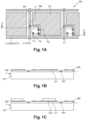
- FIGS. 1A, 1B, 1C , 1D, 1E, 1F , 1G, 1H and 1I are top and cross-sectional views illustrating steps of an example of a method of manufacturing an x-ray imaging device according to one embodiment.
- FIG. 1A is a schematic and partial top view of an embodiment of the transfer substrate 100 of the imaging device.
- THE figures 1B to 1I are cross-sectional views of the device at various stages of manufacture, along section line AA of the Figure 1A .
- the transfer substrate 100 comprises for example a support plate or sheet 101 made of an insulating material, for example glass or plastic.
- the support plate or sheet 101 comprises a conductive support, for example metallic, covered by a layer of an insulating material.
- the transfer substrate further comprises electrical connection elements, and in particular conductive tracks and conductive pads, formed on the upper face of the support plate 101. These electrical connection elements are for example formed by full plate deposition and etching of a succession of conductive and insulating levels on the upper face of the support plate 101.
- the electrical connection elements are formed by printing (or another method of localized deposition) of a succession of conductive levels and insulators on the upper face of the support plate 101.
- the transfer substrate 100 comprises two metallic conductive levels M1 and M2 separated by an insulating level I (not represented on the Figure 1A ), and metal vias V (not visible on the figure 1B ) connecting the two metallic levels M1 and M2 through the insulating level I.
- the transfer substrate 100 further comprises metallic connection pads formed on the upper metallic level M2, intended to be connected to corresponding connection pads of the elementary chips of the pixels of the device.
- Active circuits for controlling the display device suitable for powering and controlling the elementary chips of the device via the electrical connection elements of the transfer substrate, are for example connected to the electrical connection elements of the transfer substrate at the periphery of transfer substrate 100.
- the manufacture of the transfer substrate 100 comprises the following three successive steps of deposition and etching.
- a conductive layer for example metallic, for example titanium, copper or aluminum, is deposited on the upper face of the substrate 101 then etched to form the level M1.
- the level M1 comprises a plurality of conductive tracks substantially parallel to the direction of the columns of the matrix of pixels of the imaging device (vertical direction in the orientation of the Figure 1A ). More particularly, in this example, in level M1, for each column of the imaging device, a conductive track C1 is formed extending over substantially the entire length of the columns of the device. Each track C1 is intended to convey a signal VX representative of the quantity of charges photogenerated in the photodiodes of the pixels of the corresponding column, and therefore of the light intensity received by the photodiodes of the pixels of the corresponding column.
- the level M1 is covered with a layer of an insulating material, for example silicon oxide or silicon nitride, to form the insulating level I.
- an insulating material for example silicon oxide or silicon nitride
- Localized openings are then etched in the insulating layer I at the locations of the vias V, to make it possible to establish electrical connections between the M1 level and M2 level.
- the openings in the insulating layer I are for example formed by wet etching, for example of the BHF (Buffered Hydrofluoric Acid) type, or by plasma etching.
- a conductive layer for example metallic, is deposited on the upper face of the insulating level I then etched to form the level M2.
- the metallic layer of level M2 is preferably reflective.
- the metallic layer of level M2 is made of aluminium.
- the level M2 comprises a plurality of conductive tracks substantially parallel to the direction of the rows of the pixel matrix of the imaging device (horizontal direction in the orientation of the Figure 1A ). More particularly, in this example, in level M2, for each line of the imaging device, a conductive track L1 is formed extending over substantially the entire length of the lines of the device. Each track L1 is intended to convey a signal SELECT for selecting the photodiodes of the pixels of the corresponding row.
- a metal region E1 is also formed in level M2, for each pixel of the device, defining a lower electrode of the photodiode of the pixel.
- three metal pads P1, P2, P3 are formed for each pixel, on conductive areas of the metal level M2, intended to respectively receive three separate connection pads of the elementary chip of the pixel.
- the pads P1, P2, P3 are respectively connected to the conductive track L1 of the corresponding line of pixels, to the conductive track C1 of the corresponding column of pixels, and to the lower electrode E1 of the photodiode of the corresponding pixel.
- the metallic pads P1, P2, P3 can be formed immediately after the formation of the level M2, or subsequently.
- the metal studs P1, P2, P3 are formed after the production of the photodiodes of the pixels (step of the Figure 1E ).
- FIG. 1C illustrates the structure obtained at the end of a step of formation, in each pixel, of an active stack of photosensitive diode 103 on the lower electrode E1 of the photodiode of the pixel.
- Stack 103 is for example a stack of PIN diodes.
- the stack 103 is a stack based on an inorganic semiconductor material which can be deposited as a thin film on a relatively large surface, for example amorphous silicon, or indium-gallium-oxide. zinc (IGZO).
- the stack 103 is an organic photodiode stack comprising for example an organic active semiconductor layer sandwiched between two charge transport layers (not detailed in the figure).
- the inter-pixel pitch of the device in the direction of the rows and in the direction of the columns is between 50 and 500 ⁇ m, for example between 100 and 200 ⁇ m, for example of the order of 150 ⁇ m.
- the surface (in top view) occupied by the lower electrode E1 is greater than 50%, preferably greater than 70% of the surface of the pixel.
- the active photosensitive diode stack 103 covers substantially the entire surface of the electrode E1.
- the active stack 103 is for example first deposited continuously over the entire surface of the transfer substrate, then removed in a localized manner, for example by photolithography and etching, so as to retain only disjoint blocks of the stack, located opposite the lower electrodes E1 of the photodiodes of the pixels.
- FIG. 1D illustrates the structure obtained at the end of a step of formation, in each pixel, of an upper electrode E2 on the active stack of photosensitive diode 103 of the pixel.
- the electrode E2 is made of a transparent conductive material, for example a conductive transparent oxide, for example indium-tin oxide (ITO).
- ITO indium-tin oxide
- the electrodes E2 of the photodiodes PD of the pixels of the sensor are all interconnected.
- the upper electrode of the photodiodes PD is common to all the pixels of the sensor.
- the lower electrodes E1 of the various photodiodes PD are on the other hand separate, so as to allow individual reading of the photodiodes PD of the device.
- the active stack of photosensitive diode 103 is pixelated, that is to say that each pixel comprises a block formed by a portion of the stack 103 laterally separated from the portions of the stack 103 of the others. photosensitive diodes PD by isolation trenches.
- the stack 103 forms a grid extending continuously over the entire matrix of pixels, the pixelization being carried out only at the level of the lower electrodes E1 of the pixels.
- FIG. 1E illustrates the structure obtained at the end of a step of forming, in each pixel, metal connection pads P1, P2, P3 intended to be fixed and electrically connected to metal connection pads corresponding to the elementary chip of the pixel.
- pad P1 is formed on a conductive track portion of level M2 connected to column conductive track C1 of the pixel
- pad P2 is formed on a conductive track portion of level M2 connected, via 'a via V, to the line conductive track L1 of the pixel
- the pad P3 is formed on a portion of the conductive track of the level M2 connected to the lower electrode E1 of the photodiode PD of the pixel.
- the upper face of the pads P1, P2, P3 is located at a higher level than the upper face of the upper electrode E2 of the photodiodes PD of the pixels.
- the plane of the upper face of the pads P1, P2, P3 is located above the plane of the upper face of the electrodes E2 of the pixels.
- THE figures 1F And 1G illustrate a transfer step, in each pixel, of an elementary control and reading chip 153 fixed and electrically connected to the metal connection pads P1, P2, P3 of the pixel.
- the elementary chips 153 are collectively transferred from a temporary support substrate 140 to the transfer substrate 100.
- the elementary chips 153 are initially fixed to one face of the temporary support substrate 140 (lower face in the orientation of the figures).
- the structure comprising the temporary support substrate 140 and the elementary chips 153 is for example produced by a method of the type described below in relation to the figures 2A to 2E .
- Each elementary chip comprises at least one and preferably several MOS transistors, formed in and on a semiconductor substrate, for example a monocrystalline silicon substrate.
- the elementary chips 153 are for example produced in CMOS technology.
- Each elementary chip is adapted to provide, on the conductive track of column C1 of the corresponding pixel (via terminal P2), a signal, for example a voltage, representative of a light intensity received by the photodiode PD of the pixel.
- the chips 153 can be selected line by line, via the signal SELECT applied to the corresponding conductive track L1, so as to read the photodiodes PD line by line during an image acquisition phase.
- the elementary chips 153 are attached collectively opposite the connection face of the transfer substrate 100, namely its upper face in the orientation of the figures, using the temporary support substrate 140 as a handle ( figure 1F ).
- connection pads 143 of elementary chips 153 located on the side of the lower face of said chips, are then brought into contact with the corresponding connection pads P1, P2, P3 of the transfer substrate 100, and fixed to said connection pads P1, P2, P3.
- the fixing of the connection pads 143 of the elementary chips 153 to the connection pads of the transfer substrate is for example carried out by direct bonding, by thermocompression, by soldering, by means of metal microstructure (for example micro-pillars) formed beforehand on the studs 143, or by any other suitable fixing and connection method, for example by connection by means of a conductive film of the AFC type (from the English "Anisotropic Conducting Film" - anisotropic conductive film).
- the elementary chips 153 are detached from the temporary support substrate 140, and the latter is removed ( figure 1G ), releasing access to the illumination face of the photodiodes PD.
- the pitch of the elementary chips 153 on the transfer substrate 100 can be greater than the pitch of the elementary chips 153 on the temporary support substrate 140.
- the pitch of the elementary chips 153 on the transfer substrate 100 is a multiple of the pitch of the elementary chips 153 on the temporary support substrate 140. In this case, only a part of the chips 153 is removed from the support substrate 140 at each transfer, as illustrated in the figures 1F And 1G .
- the other chips 153 remain attached to the temporary support substrate 140 and can be used during another collective transfer step to populate another part of the transfer substrate 100 or another transfer substrate.
- FIG. 1G illustrates a step of depositing a planarization layer 170 on the structure obtained at the end of the steps of figures 1A to 1G .
- the material of layer 170 is a transparent dielectric material, for example a polymer material.
- the material of the layer 170 extends from the upper face of the support substrate, to a height greater than that of the upper face of the elementary chips 153. Thus, the material of the layer 170 completely covers the support substrate, the photodiodes PD, and the elementary chips 153.
- the upper face of the layer 170 is substantially flat and extends continuously over the entire surface of the pixel array.
- the scintillator 180 comprises a layer of a scintillation material, for example iodide of cesium (CsI) in crystalline form, gadolinium oxide (GadOx), or any other suitable scintillation material, i.e. a material emitting light following energy deposition by interaction with X-rays, extending continuously over the entire surface of the transfer substrate 100.
- a scintillation material for example iodide of cesium (CsI) in crystalline form, gadolinium oxide (GadOx), or any other suitable scintillation material, i.e. a material emitting light following energy deposition by interaction with X-rays, extending continuously over the entire surface of the transfer substrate 100.
- the scintillation layer may have a thickness comprised between 200 ⁇ m and 1 mm depending on the intended applications, for example of the order of 600 ⁇ m.
- the thickness of the PD photodiodes is for example between 1 and 10 ⁇ m, for example between 1 and 2 ⁇ m for photodiodes based on amorphous silicon, or indium-gallium-zinc oxide (IGZO), and between 1 and 5 ⁇ m for organic photodiodes.
- the thickness of the elementary chips 153 is for example between 100 ⁇ m and 500 ⁇ m.
- the lateral dimensions of the elementary chips 153 are for example between 5 and 150 ⁇ m, for example between 10 and 60 ⁇ m.
- the scintillator 180 is for example formed separately on a growth substrate, then transferred onto the upper face of the passivation layer 170. Alternatively, the scintillator 180 is formed directly on the upper face of the passivation layer 170.
- THE figures 2A, 2B, 2C, 2D and 2E are cross-sectional views illustrating successive steps of an example of a method for manufacturing elementary chips 153 of an X-ray imaging device of the type described in relation to the figures 1A to 1I .
- FIG. 2A schematically represents a control structure comprising a first substrate 201 in and on which have been formed a plurality of elementary control integrated circuits 203, for example identical or similar, corresponding respectively to the control integrated circuits of the future elementary chips 153 of the pixels of the device.
- the substrate 201 is an SOI type substrate (from the English "Semiconductor On Insulator" - semiconductor on insulator), comprising a semiconductor support substrate 201a, for example made of silicon, an insulating layer 201b, for example of silicon oxide, arranged on and in contact with the upper face of the support substrate 201a, and an upper semiconductor layer 201c, for example of monocrystalline silicon, arranged on and in contact with the upper face of the insulating layer 201b.
- SOI type substrate from the English "Semiconductor On Insulator" - semiconductor on insulator
- the elementary control circuits 203 are formed in and on the upper semiconductor layer 201c of the substrate 201.
- Each elementary control circuit 203 comprises for example one or more MOS transistors (not detailed in the figures).
- the elementary control circuits 203 are for example produced in CMOS technology (standing for “Complementary Metal Oxide Semiconductor”).
- Each elementary control circuit 203 can comprise a circuit for reading a photodiode PD of the imaging device.
- FIG. 2B illustrates the structure obtained at the end of a stage of transferring and fixing the structure of the figure 2A on the temporary support substrate 140.
- the temporary support substrate 140 comprises a first layer 140a of a support material, for example glass or silicon, with a thickness comprised, for example, between 200 and 700 ⁇ m, and a second layer 140b, thinner, in an adhesive material with relatively low adhesion to allow the selective detachment of the elementary chips during the collective transfer step of the figures 1F And 1G , for example a polymeric material.
- layer 140b is disposed on and in contact with the top face of layer 140a.
- the structure comprising the control circuits 203 is fixed to the upper face of the layer 140b by its lower face, namely its face opposite the support 201a (corresponding to its upper face in the orientation of the figure 2A ).
- FIG. 2C illustrates the structure obtained after a step of removing the support 101c from the initial SOI structure, for example by grinding and/or chemical etching, so as to free up access to the upper face of the insulating layer 201b of the SOI structure.
- the substrate 201 is an SOI type substrate.
- the substrate 201 can be a solid semiconductor substrate, for example made of silicon.
- the substrate 201 can be thinned by its rear face (upper face in the orientation of the Fig. 2C ), for example by grinding.
- An insulating passivation layer for example of silicon oxide, can then be deposited on the upper face of the thinned substrate, replacing the layer 201b of the SOI substrate.
- FIG. 2D figure illustrates the structure obtained at the end of steps of forming contact recovery openings in layers 201b and 201c, and of forming contact recovery metallizations 143 in and on said openings.
- the metallizations 143 make it possible to resume electrical contacts on the metallic levels (not detailed in the figures) of the interconnection stack arranged on the side of the lower face of the semiconductor layer 201c.
- the metallizations 143 are for example electrically connected to transistors of the control circuit, these transistors being themselves connected or electrically linked to connection metallizations 205 of circuits 203.
- the metallizations 143 form connection terminals of the future elementary chips of the pixels of the device, intended to be connected to corresponding connection terminals of the transfer substrate 100 of the device.
- FIG. 2E illustrates the structure obtained at the end of a step of singularization of the elementary pixel chips of the device.
- trenches 151 extending vertically through layers 201b and 201c are formed from the upper face of the structure, along cut lines.
- the trenches open onto the upper face of the temporary support substrate 140.
- the trenches 151 form a continuous grid laterally delimiting a plurality of elementary pixel chips 153, for example identical or similar, each comprising a elementary control circuit 203.
- the trenches 151 are for example made by plasma etching.
- the elementary chips 153 are intended to be transferred onto the transfer substrate 100 of the X-ray imaging device, as described above in relation to the figures 1A to 1I .
- FIGS. 3A, 3B, 3C, 3D , 3E and 3F are top and cross-sectional views illustrating steps of another example of a method of manufacturing an x-ray imaging device according to one embodiment.
- the process of figures 3A to 3F differs from the process of figures 1A to 1I chiefly in that, in the process of figures 3A to 3F , the elementary chips 153 of the pixels are transferred onto the transfer substrate 100 before the formation PD photodiodes, and not afterwards as in the example of the figures 1A to 1I .
- FIG. 3A is a schematic and partial top view of an embodiment of the transfer substrate 100 of the imaging device.
- the transfer substrate 100 comprises two conductive metal levels M1 and M2 separated by an insulating level I, and metal vias V connecting the two metal levels M1 and M2 through the insulating level I.
- the transfer substrate 101 further comprises metallic connection pads formed on the upper metallic level M2, intended to be connected to corresponding connection pads of the elementary chips of the pixels of the device.
- the level M1 comprises, for each column of pixels of the imaging device, a conductive track C1 extending over substantially the entire length of the columns of the device, intended to convey a signal VX representative of the light intensity received by the photodiodes of the pixels of the corresponding column
- the level M2 comprises, for each row of pixels of the imaging device, a conductive track L1 extending over substantially the entire length of the rows of the device, intended to convey a signal SELECT for selecting the photodiodes of the pixels of the corresponding line.
- a metal region CT defining a contact recovery region intended to be electrically connected to a lower electrode of the pixel photodiode.
- the region CT does not directly constitute the lower electrode of the photodiode of the pixel.
- the region CT may have a surface area smaller than that of the lower electrode E1 of the photodiode of the pixel.
- three metallic pads P1, P2, P3 intended to respectively receive three separate connection pads of the elementary chip of the pixel are formed, for each pixel, on conductive zones of the metallic level M2.
- the pads P1, P2, P3 are respectively connected to the conductive track L1 of the corresponding row of pixels, to the conductive track C1 of the corresponding column of pixels, and to the contact recovery region CT on the lower electrode of the photodiode of the corresponding pixel.
- connection pads P1, P2, P3 can be formed directly by portions of the level M2.
- the pad P1 is connected to the conductive track of column C1 of the pixel via a portion of conductive track of the level M2
- the pad P2 is connected to the conductive track of line L1 of the pixel by the intermediate a portion of conductive track of level M2 and a via V
- pad P3 is connected to region CT by a portion of conductive track of level M2.
- FIG. 3B illustrates the structure obtained at the end of a transfer step, in each pixel, of an elementary control and reading chip 153 fixed and electrically connected to the metal connection pads P1, P2, P3 of the pixel.
- the chips 153 are for example transferred collectively from a temporary support substrate, in a manner similar to what has been described above in relation to the figures 1F And 1G .
- Fig. 3C illustrates a step of depositing a planarization layer 170 on the structure obtained at the end of the steps of figures 3A and 3B .
- the material of layer 170 is a dielectric material, transparent or not, for example a polymer material.
- the material of the layer 170 extends from the upper face of the support substrate, to a height greater than that of the upper face of the elementary chips 153. Thus, the material of the layer 170 completely covers the support substrate and the elementary chips 153.
- the upper face of the layer 170 is substantially flat and extends continuously over the entire surface of the transfer substrate 100.
- FIG. 3C further illustrates a step of forming, in each pixel, a conductive via 301 extending vertically through the layer 170.
- the via 301 is in contact, by its lower face, with the upper face of the contact region CT .
- the upper face of via 301 is flush with the upper face of layer 170.
- the electrode E1, the active stack 103, and the upper electrode E2 are for example identical or similar to this which has been described above in connection with the Figures 1B, 1C And 1D .
- the lower electrode E1 In each pixel, the lower electrode E1 is in contact, via its lower face, with the upper face of via 301 of the pixel. Thus, the lower electrode E1 is electrically connected to the contact recovery region CT of the pixel (and therefore the elementary chip 153 of the pixel) via the via 301.
- the stack formed by the lower electrode E1, the active stack 103 and the upper electrode E2 defines a photodiode PD of the pixel.
- the electrodes E2 of the photodiodes PD of the pixels of the sensor are all interconnected.
- the upper electrode of the photodiodes PD is common to all the pixels of the sensor.
- the lower electrodes E1 of the various photodiodes PD are on the other hand separate, so as to allow individual reading of the photodiodes PD of the device.
- the photodiode PD and more particularly the active stack 103 of the photodiode PD, extend above the elementary chip 153 of the pixel.
- the active stack of photosensitive diode 103 is pixelated, that is to say that each pixel comprises a block formed by a portion of the stack 103 laterally separated from the portions of the stack 103 of the others. photosensitive diodes PD by isolation trenches.
- the stack 103 extends so as to continuous over the entire matrix of pixels, the pixelation being carried out only at the level of the lower electrodes E1 of the pixels.
- FIG 3F illustrates the structure obtained at the end of a step of depositing a scintillator 180, for example identical or similar to that of the figure 1I , above the PD photodiodes.
- the scintillator 180 is deposited directly above the PD photodiodes, without an intermediate planarization layer.
- a transparent planarization layer may be deposited over the PD photodiodes before the scintillator 180 is deposited.
- FIG. 4 is a cross-sectional view illustrating a variant of the method of Figures 3A, 3B, 3C, 3D , 3E and 3F .
- the electrical connection between the elementary chip 153 and the lower electrode E1 of the photodiode PD of the pixel is made via a metal connection terminal 143' of the elementary chip, located in upper surface of the elementary chip.
- the connection terminal 143' is flush with the level of the upper face of the planarization layer 170.
- the connection terminal 143' is in contact, via its upper face, with the lower face of the electrode E1.
- THE figures 5A and 5B are top and cross-sectional views illustrating steps of another example of a method of manufacturing an x-ray imaging device according to one embodiment.
- FIG. 5A is a schematic and partial top view of an embodiment of the transfer substrate 100 of the imaging device.
- FIG. 5B is a cross-sectional view of the device along section line AA of the figure 5A .
- each elementary chip 153 attached to the transfer substrate comprises not only an integrated circuit for controlling and reading the photodiode PD of the pixel, but also an inorganic light-emitting diode (LED), and an integrated circuit for controlling the LED.
- the integration of an LED in the elementary chip 153 advantageously makes it possible to implement, between two image acquisition phases, a step of reinitializing the photodiodes PD by applying a light flash to the photodiodes PD.
- the elementary chips 153 are monolithic pixel chips, for example of the type described in the patent applications WO2017089676 , EP3401958 And WO2018185433 previously filed.
- Each chip comprises an LED 501 and an elementary control circuit 503 attached and electrically connected to the LED.
- the control circuit 503 is for example made in CMOS technology.
- Circuit 503 includes for example a circuit for controlling and reading the photodiode PD of the pixel, and an LED control circuit.
- the LED 501 covers the upper face of the elementary control circuit 503.
- the circuit 503 includes connection terminals 143 on the side of its lower face.
- the LED 501 is covered, on the side of its upper face, by an opaque or reflective layer 505, for example made of metal.
- Layer 505 makes it possible to direct the light emitted by the LED in the direction of the photodiode PD of the pixel.
- Layer 505 for example forms the upper electrode of LED 501.
- the planarization layer 170 ( figure 5B ) is made of a transparent material.
- the transfer substrate 100 of the example of the figures 5A and 5B comprises a number of conductive tracks and connection metallizations greater than that of the example of figures 1A to 1I .
- the elementary chips 153 comprise a greater number of connection terminals than what has been described previously.
- each elementary chip comprises six connection terminals intended to be connected respectively to six metal connection pads P1, P2, P3, P4, P5, P6 of the transfer substrate 100.
- the level M1 comprises, for each column of pixels of the imaging device, three conductive column tracks C1, C2, C3 intended to convey respectively a signal VX representative of the light intensity received by the photodiodes of the pixels of the corresponding column, a signal DATA for controlling the LEDs of the pixels of the corresponding column, and a signal VDD for supplying the LEDs of the pixels of the corresponding column.
- the level M2 comprises, for each line of pixels of the imaging device, two line conductive tracks L1 and L2 intended to convey respectively a signal SELPD for selecting the photodiodes of the pixels of the corresponding line, and a signal SELLED for selecting of the LEDs of the pixels of the corresponding line.
- the metal pads P1, P2, P3, P4, P5, P6 are formed on conductive areas of the metal level M2 and are intended to respectively receive six separate connection pads of the elementary chip of the pixel.
- the pads P1, P2, P3, P4, P5, P6 are respectively connected to the conductive track L1 of the corresponding line of pixels, to the conductive track L2 of the corresponding line of pixels, to the electrode E1 of the photodiode PD of the corresponding pixel, to the conductive track C3 of the corresponding column of pixels, to the conductive track C4 of the corresponding column of pixels, and to the conductive track C5 of the corresponding column of pixels.
- the elementary chips 153 are fixed and electrically connected to the transfer substrate 100 before the formation of the photodiodes PD of the pixels.
- THE figures 6A and 6B are top and cross-sectional views illustrating steps of an alternative embodiment of the method of figures 5A and 5B , in which the elementary chips are fixed and electrically connected to the substrate of the transfer after the formation of the photodiodes PD, in a manner similar to what has been described above in relation to the figures 3A to 3F .
- the reflective layer 505 of the figure 5B can be omitted or replaced by a transparent layer, for example a layer transparent conductor, for example made of ITO, forming the upper electrode of the LED 501.
- a transparent layer for example a layer transparent conductor, for example made of ITO, forming the upper electrode of the LED 501.
- the elementary LED 501 of the pixel is located directly under the photodiode PD of the pixel.
- the planarization layer 170 ( figure 6B ) is made of a transparent material.
- FIG 7 is a sectional view illustrating another alternative embodiment of an X-ray imaging device according to one embodiment.
- the device comprises two devices of the type described in connection with the figure 1I , superimposed.
- the device of the figure 7 makes it possible to perform dual-energy X-ray imaging, also called color X-ray imaging, i.e. to image respectively a first energy level, called low-energy (BE) level, by means of the upper imaging device, and a second energy level, called high energy (HE) level, by means of the lower imaging device.
- dual-energy X-ray imaging also called color X-ray imaging, i.e. to image respectively a first energy level, called low-energy (BE) level, by means of the upper imaging device, and a second energy level, called high energy (HE) level, by means of the lower imaging device.
- BE low-energy
- HE high energy
- the upper imaging device is suitable for detecting radiation with an energy level of between 1 keV and 140 keV, for example between 40 keV and 80 keV, for example of the order of 60 keV in average
- the lower imaging device is suitable for detecting radiation with an energy level of between 60 keV and 140 keV, for example between 80 keV and 120 keV, for example of the order of 100 keV on average.
- an interface layer 701 is arranged between the lower face of the support substrate 101 of the upper device and the upper face of the scintillator 180 of the lower device.
- the thickness of the support substrate of the upper device is preferably relatively low to limit the absorption of high energy photons.
- the thickness of the support substrate of the upper device is less than the thickness of the support substrate of the lower device.
- the interface layer 710 can comprise a filtering layer adapted to filter the low-energy radiation so that only the high-energy radiation reaches the lower imaging device.
- the filtering layer is for example a metal layer, for example continuous, for example copper or aluminum, for example with a thickness of between 0.1 and 0.4 mm. The filtering layer makes it possible to improve the spectral separation between the two imaging devices.
- interface layer 701 can be omitted.
- a scintillator 180 covers a matrix of pixels each comprising a monolithic elementary chip and a photodiode.
- the detector comprises an active detection stack based on a scintillator material 180 adapted to directly convert X photons into light photons, for example a material from the group comprising Cesium Iodide (CsI:Tl) or GADOX (Gd2O2S:Tb), which light photons then interact with the photodiode of the pixel to generate electrons.
- Cesium Iodide CsI:Tl
- GADOX Gd2O2S:Tb
Abstract
La présente description concerne un dispositif d'imagerie à rayons X, comportant :- un substrat de report (100) comportant des éléments de connexion électrique ;- une matrice de pixels comportant chacun une puce élémentaire monolithique (153) fixée et connectée électriquement à des éléments de connexion électrique du substrat de report (100), et une photodiode (PD) formée sur le substrat de report et connectée électriquement à la puce élémentaire (153) ; et- un scintillateur (180) revêtant la matrice de pixels,dans lequel, dans chaque pixel, la puce élémentaire (153) comprend un circuit intégré de lecture de la photodiode (PD) du pixel.The present description relates to an X-ray imaging device, comprising:- a transfer substrate (100) comprising electrical connection elements;- a matrix of pixels each comprising a monolithic elementary chip (153) fixed and electrically connected to electrical connection elements of the transfer substrate (100), and a photodiode (PD) formed on the transfer substrate and electrically connected to the elementary chip (153); and- a scintillator (180) covering the matrix of pixels, in which, in each pixel, the elementary chip (153) comprises an integrated circuit for reading the photodiode (PD) of the pixel.
Description
La présente description concerne un dispositif d'imagerie à rayons X et un procédé de fabrication d'un tel dispositif, notamment pour des applications de radiographie, par exemple dans le domaine de l'imagerie médicale.The present description concerns an X-ray imaging device and a method for manufacturing such a device, in particular for radiography applications, for example in the field of medical imaging.
Parmi les dispositifs d'imagerie à rayons X connus, on peut distinguer les dispositifs à conversion indirecte et les dispositifs à conversion directe.Among known X-ray imaging devices, indirect conversion devices and direct conversion devices can be distinguished.
Les dispositifs à conversion indirecte comprennent une matrice de photodiodes adaptées à capter un rayonnement lumineux, et un scintillateur disposé au-dessus de la matrice de photodiodes. En fonctionnement, le scintillateur émet de la lumière suite à l'absorption des rayons X. La lumière émise par le scintillateur est convertie en charges électriques par les photodiodes. Ainsi, la matrice de photodiodes acquiert une image représentative de la distribution lumineuse émise par le scintillateur, cette distribution lumineuse étant elle-même représentative de la distribution de rayon X reçue par le scintillateur.Indirect conversion devices comprise a matrix of photodiodes adapted to capture light radiation, and a scintillator arranged above the matrix of photodiodes. In operation, the scintillator emits light following the absorption of X-rays. The light emitted by the scintillator is converted into electrical charges by the photodiodes. Thus, the array of photodiodes acquires an image representative of the light distribution emitted by the scintillator, this light distribution itself being representative of the X-ray distribution received by the scintillator.
Les dispositifs à conversion directe comprennent une couche d'un matériau semiconducteur de conversion adapté à convertir directement les rayons X absorbés, en charges électrique. La couche de conversion est disposée au-dessus d'une matrice de circuits élémentaires adaptée à lire les charges électriques générées dans le matériau de conversion. En fonctionnement la couche de conversion génère des charges électriques suite à l'absorption des rayons X. Ces charges sont lues par la matrice de circuits de lecture. Ainsi, la matrice de circuits de lecture acquiert directement une image représentative de la distribution de rayons X reçue par le matériau de conversion.Direct conversion devices include a layer of a conversion semiconductor material suitable for directly converting the absorbed X-rays into electrical charges. The conversion layer is arranged above a matrix of elementary circuits adapted to read the electric charges generated in the conversion material. In operation, the conversion layer generates electrical charges following the absorption of X-rays. These charges are read by the matrix of read circuits. Thus, the matrix of read circuits directly acquires an image representative of the X-ray distribution received by the conversion material.
On s'intéresse ici plus particulièrement à la réalisation de dispositifs d'imagerie à rayons X à conversion indirecte.We are more particularly interested here in the production of X-ray imaging devices with indirect conversion.
Un mode de réalisation prévoit un dispositif d'imagerie à rayons X, comportant :
- un substrat de report comportant des éléments de connexion électrique ;
- une matrice de pixels comportant chacun une puce élémentaire monolithique fixée et connectée électriquement à des éléments de connexion électrique du substrat de report, et une photodiode formée sur le substrat de report et connectée électriquement à la puce élémentaire ; et
- un scintillateur revêtant chaque pixel,
- a transfer substrate comprising electrical connection elements;
- a matrix of pixels each comprising a monolithic elementary chip fixed and electrically connected to electrical connection elements of the transfer substrate, and a photodiode formed on the transfer substrate and electrically connected to the elementary chip; And
- a scintillator coating each pixel,
Selon un mode de réalisation, dans chaque puce élémentaire, le circuit intégré de lecture de la photodiode du pixel est réalisé en technologie CMOS.According to one embodiment, in each elementary chip, the integrated circuit for reading the photodiode of the pixel is produced in CMOS technology.
Selon un mode de réalisation, dans chaque pixel, la photodiode comprend un empilement actif à base d'un matériau semiconducteur inorganique, par exemple du silicium amorphe ou de l'oxyde d'indium-gallium-zinc.According to one embodiment, in each pixel, the photodiode comprises an active stack based on an inorganic semiconductor material, for example amorphous silicon or indium-gallium-zinc oxide.
Selon un mode de réalisation, dans chaque pixel, la photodiode comprend un empilement actif de diode photosensible organique.According to one embodiment, in each pixel, the photodiode comprises an active stack of organic photosensitive diode.
Selon un mode de réalisation, dans chaque pixel, la photodiode comprend une électrode supérieure en un matériau transparent.According to one embodiment, in each pixel, the photodiode comprises an upper electrode made of a transparent material.
Selon un mode de réalisation, dans chaque pixel, la photodiode ne recouvre pas la puce élémentaire du pixel.According to one embodiment, in each pixel, the photodiode does not cover the elementary chip of the pixel.
Selon un mode de réalisation, dans chaque pixel, la photodiode recouvre la puce élémentaire du pixel.According to one embodiment, in each pixel, the photodiode covers the elementary chip of the pixel.
Selon un mode de réalisation, dans chaque pixel, la puce élémentaire du pixel comprend une LED inorganique et un circuit intégré de contrôle de la LED.According to one embodiment, in each pixel, the elementary chip of the pixel comprises an inorganic LED and an integrated circuit for controlling the LED.
Un autre mode de réalisation prévoir un assemblage comportant des premier et deuxième dispositifs d'imagerie à rayons X tels que définis ci-dessus, superposés.Another embodiment provides an assembly comprising first and second X-ray imaging devices as defined above, superimposed.
Selon un mode de réalisation, l'assemblage comprend une couche de filtrage entre les premier et deuxième dispositifs.According to one embodiment, the assembly comprises a filtering layer between the first and second devices.
Un autre mode de réalisation prévoit un procédé de fabrication d'un dispositif d'imagerie à rayons X tel que défini ci-dessus, dans lequel les puces élémentaires sont reportées et fixées collectivement au substrat de report, au moyen d'un substrat de support temporaire.Another embodiment provides a method for manufacturing an X-ray imaging device as defined above, in which the elementary chips are transferred and fixed collectively to the transfer substrate, by means of a support substrate temporary.
Selon un mode de réalisation, le procédé comprend la formation des photodiodes des pixels sur le substrat de report avant l'étape de report collectif des puces élémentaires sur le substrat de report.According to one embodiment, the method comprises the formation of the photodiodes of the pixels on the transfer substrate before the step of collective transfer of the elementary chips onto the transfer substrate.
Selon un mode de réalisation, le procédé comprend la formation des photodiodes des pixels sur le substrat de report après l'étape de report collectif des puces élémentaires sur le substrat de report.According to one embodiment, the method comprises the formation of the photodiodes of the pixels on the transfer substrate after the step of collective transfer of the elementary chips onto the transfer substrate.
Ces caractéristiques et leurs avantages, ainsi que d'autres, seront exposés en détail dans la description suivante de modes de réalisation particuliers faite à titre non limitatif en relation avec les figures jointes parmi lesquelles :
- les
figures 1A, 1B, 1C ,1D, 1E, 1F ,1G, 1H et 1I sont des vues de dessus et en coupe illustrant des étapes d'un exemple d'un procédé de fabrication d'un dispositif d'imagerie à rayons X selon un mode de réalisation ; - les
figures 2A, 2B, 2C, 2D et 2E sont des vues en coupe illustrant des étapes d'un exemple d'un procédé de fabrication de puces élémentaires de pixel d'un dispositif d'imagerie à rayons X selon un mode de réalisation ; - les
figures 3A, 3B, 3C, 3D ,3E et 3F sont des vues de dessus et en coupe illustrant des étapes d'un autre exemple d'un procédé de fabrication d'un dispositif d'imagerie à rayons X selon un mode de réalisation ; - la
figure 4 est une vue en coupe illustrant une variante du procédé desfigures 3A, 3B, 3C, 3D ,3E et 3F ; - les
figures 5A et 5B sont des vues de dessus et en coupe illustrant des étapes d'un autre exemple d'un procédé de fabrication d'un dispositif d'imagerie à rayons X selon un mode de réalisation ; - les
figures 6A et 6B sont des vues de dessus et en coupe illustrant des étapes d'un autre exemple d'un procédé de fabrication d'un dispositif d'imagerie à rayons X selon un mode de réalisation ; et - la
figure 7 est une vue en coupe illustrant une variante d'un dispositif d'imagerie à rayons X selon un mode de réalisation.
- THE
Figures 1A, 1B, 1C ,1D, 1E, 1F ,1G, 1H and 1I are top and cross-sectional views illustrating steps of an example of a method of manufacturing an X-ray imaging device according to one embodiment; - THE
figures 2A, 2B, 2C, 2D and 2E are cross-sectional views illustrating the steps of an example of a method for manufacturing elementary pixel chips of an X-ray imaging device according to one embodiment; - THE
Figures 3A, 3B, 3C, 3D ,3E and 3F are top and cross-sectional views illustrating steps of another example of a method of manufacturing an X-ray imaging device according to one embodiment; - there
figure 4 is a cross-sectional view illustrating a variant of the method ofFigures 3A, 3B, 3C, 3D ,3E and 3F ; - THE
figures 5A and 5B are top and cross-sectional views illustrating steps of another example of a method of manufacturing an X-ray imaging device according to one embodiment; - THE
figures 6A and 6B are top and cross-sectional views illustrating steps of another example of a method of manufacturing an X-ray imaging device according to one embodiment; And - there
figure 7 is a sectional view illustrating a variation of an X-ray imaging device according to one embodiment.
De mêmes éléments ont été désignés par de mêmes références dans les différentes figures. En particulier, les éléments structurels et/ou fonctionnels communs aux différents modes de réalisation peuvent présenter les mêmes références et peuvent disposer de propriétés structurelles, dimensionnelles et matérielles identiques.The same elements have been designated by the same references in the various figures. In particular, the structural and/or functional elements common to the different embodiments may have the same references and may have identical structural, dimensional and material properties.
Par souci de clarté, seuls les étapes et éléments utiles à la compréhension des modes de réalisation décrits ont été représentés et sont détaillés. En particulier, les diverses applications que peuvent avoir les dispositifs d'imagerie à rayons X décrits n'ont pas été détaillées, les modes de réalisation décrits étant compatibles avec toutes ou la plupart des applications connues d'imagerie à rayons X, et tout particulièrement les applications pouvant tirer profit de dispositif d'imagerie à rayons X de grandes dimensions, par exemple des dispositifs de dimensions latérales supérieures à 10 cm et de préférence supérieures à 20 cm. En outre, la réalisation des diodes photosensibles, des circuits électroniques de contrôle, et du scintillateur des dispositifs décrits n'ont pas été détaillés, la réalisation de ces éléments étant à la portée de la personne du métier à partir des indications de la présente description. Par rayons X on entend ici, par exemple, des rayonnements constitués de photons d'énergie comprise, par exemple, entre 1000 eV (électron-volt) et 20 MeV (méga-électron-volt).For the sake of clarity, only the steps and elements useful for understanding the embodiments described have been represented and are detailed. In particular, the various applications that the described X-ray imaging devices may have have not been detailed, the described embodiments being compatible with all or most of the known X-ray imaging applications, and most particularly applications that can take advantage of large X-ray imaging devices, for example devices with lateral dimensions greater than 10 cm and preferably greater than 20 cm. In addition, the realization of the photosensitive diodes, the electronic control circuits, and the scintillator of the devices described have not been detailed, the realization of these elements being within the reach of the person skilled in the art from the indications of this description. . By X-rays is meant here, for example, radiation consisting of photons of energy comprised, for example, between 1000 eV (electron-volt) and 20 MeV (mega-electron-volt).
Sauf précision contraire, lorsque l'on fait référence à deux éléments connectés entre eux, cela signifie directement connectés sans éléments intermédiaires autres que des conducteurs, et lorsque l'on fait référence à deux éléments reliés (en anglais "coupled") entre eux, cela signifie que ces deux éléments peuvent être connectés ou être reliés par l'intermédiaire d'un ou plusieurs autres éléments.Unless otherwise specified, when reference is made to two elements connected together, this means directly connected without intermediate elements other than conductors, and when reference is made to two elements connected (in English "coupled") between them, this means that these two elements can be connected or be linked through one or more other elements.
Dans la description qui suit, lorsque l'on fait référence à des qualificatifs de position absolue, tels que les termes "avant", "arrière", "haut", "bas", "gauche", "droite", etc., ou relative, tels que les termes "dessus", "dessous", "supérieur", "inférieur", etc., ou à des qualificatifs d'orientation, tels que les termes "horizontal", "vertical", etc., il est fait référence sauf précision contraire à l'orientation des vues en coupe des figures.In the following description, when referring to absolute position qualifiers, such as "front", "rear", "up", "down", "left", "right", etc., or relative, such as the terms "above", "below", "upper", "lower", etc., or to qualifiers of orientation, such as the terms "horizontal", "vertical", etc., unless otherwise specified, reference is made to the orientation of the sectional views of the figures.
Sauf précision contraire, les expressions "environ", "approximativement", "sensiblement", et "de l'ordre de" signifient à 10 % près, de préférence à 5 % près.Unless specified otherwise, the expressions “about”, “approximately”, “substantially”, and “of the order of” mean to within 10%, preferably within 5%.
Selon un aspect des modes de réalisation décrits, on prévoit un dispositif d'imagerie à rayons X comportant un substrat de report, une matrice de pixels de photo-détection formée sur le substrat de report, et un scintillateur revêtant la matrice de pixels de photo-détection. Chaque pixel de photo-détection comprend une photodiode formée sur le substrat de report et reliée ou connectée électriquement à des éléments de connexion électrique (piste, plages, bornes ou plots de connexion électrique) du substrat de report, et une puce élémentaire monolithique, fixée et connectée électriquement à des éléments de connexion électrique du substrat de report. Dans chaque pixel, la puce élémentaire est connectée à la photodiode, par exemple par au moins un élément de connexion électrique du substrat de report. La puce élémentaire comprend au moins un circuit intégré de lecture de la photodiode du pixel, de préférence réalisé en technologie CMOS.According to one aspect of the described embodiments, an X-ray imaging device is provided comprising a transfer substrate, an array of photo-detection pixels formed on the transfer substrate, and a scintillator coating the array of photo-detection pixels -detection. Each photo-detection pixel comprises a photodiode formed on the transfer substrate and connected or electrically connected to electrical connection elements (track, pads, terminals or electrical connection pads) of the transfer substrate, and a monolithic elementary chip, fixed and electrically connected to electrical connection elements of the transfer substrate. In each pixel, the elementary chip is connected to the photodiode, for example by at least one electrical connection element of the transfer substrate. The elementary chip comprises at least one integrated circuit for reading the photodiode of the pixel, preferably made in CMOS technology.
Chaque puce élémentaire comporte une face de connexion comprenant une pluralité de plots (aussi appelées bornes ou plages) de connexion électrique destinés à être connectés au substrat de report pour la commande de la puce. Le substrat de report comprend une face de connexion comportant, pour chaque puce élémentaire, une pluralité de plots (aussi appelées bornes ou plages) de connexion électrique destinés à être connectés respectivement aux plots de connexion électrique de la puce. Les puces sont rapportées sur le substrat de report, faces de connexion tournées vers la face de connexion du substrat de report, et fixées sur le substrat de report de façon à connecter les plots de connexion électrique de chaque puce aux plots de connexion électrique correspondants du substrat de report.Each elementary chip has a connection face comprising a plurality of electrical connection pads (also called terminals or pads) intended to be connected to the transfer substrate for controlling the chip. The transfer substrate comprises a connection face comprising, for each elementary chip, a plurality of electrical connection pads (also called terminals or pads) intended to be connected respectively to the electrical connection pads of the chip. The chips are reported on the transfer substrate, connection faces facing the connection face of the transfer substrate, and fixed on the transfer substrate so as to connect the electrical connection pads of each chip to the corresponding electrical connection pads of the transfer substrate.
Un avantage des modes de réalisation décrits est qu'ils permettent d'obtenir des dispositifs d'imagerie de grandes dimensions, par exemple de dimensions latérales supérieures à 10 cm et de préférence supérieures à 20 cm, à des coûts relativement faibles, tout en bénéficiant des avantages des circuits intégrés monolithiques, par exemple des circuits CMOS, pour la lecture des photodiodes. Un avantage réside notamment dans le faible bruit de lecture introduit par de tels circuits intégrés monolithiques par rapport à des circuits à base de transistors TFT (de l'anglais "Thin Film Transistor" - transistor en couches minces), formés par dépôts successifs de plusieurs couches minces directement sur le substrat de report. Un autre avantage est un gain en rapidité de lecture, lié à la meilleure mobilité des porteurs de charge dans de tels circuits intégrés monolithiques par rapport à des circuits TFT. En outre, de tels circuits permettent, de façon optionnelle, de mettre en œuvre des fonctions additionnelles de traitement des signaux électriques fournis par les photodiodes. Un autre avantage réside dans le faible encombrement des puces élémentaires monolithique par rapport à des circuits TFT.An advantage of the embodiments described is that they make it possible to obtain imaging devices of large dimensions, for example of lateral dimensions greater than 10 cm and preferably greater than 20 cm, at relatively low costs, while benefiting advantages of monolithic integrated circuits, for example CMOS circuits, for reading photodiodes. One advantage lies in particular in the low reading noise introduced by such monolithic integrated circuits compared to circuits based on TFT transistors (from the English "Thin Film Transistor" - thin film transistor), formed by successive deposits of several thin layers directly on the transfer substrate. Another advantage is a gain in reading speed, linked to the better mobility of the charge carriers in such monolithic integrated circuits compared to TFT circuits. In addition, such circuits make it possible, optionally, to implement additional functions for processing the electrical signals supplied by the photodiodes. Another advantage lies in the small size of monolithic elementary chips compared to TFT circuits.
Des exemples de réalisation d'un tel dispositif d'imagerie à rayons X vont être décrits plus en détail ci-après en relation avec les figures.Examples of embodiments of such an X-ray imaging device will be described in more detail below in relation to the figures.
Les
La
Sur la
Les
Le substrat de report 100 comprend par exemple une plaque ou feuille de support 101 en un matériau isolant, par exemple en verre ou en plastique. A titre de variante, la plaque ou feuille de support 101 comprend un support conducteur, par exemple métallique, recouvert par une couche d'un matériau isolant. Le substrat de report comprend en outre des éléments de connexion électrique, et en particulier des pistes conductrices et des plots conducteurs, formés sur la face supérieure de la plaque de support 101. Ces éléments de connexion électrique sont par exemple formés par dépôt pleine plaque et gravure d'une succession de niveaux conducteurs et isolants sur la face supérieure de la plaque de support 101. A titre de variante, les éléments de connexion électrique sont formés par impression (ou autre méthode de dépôt localisé) d'une succession de niveaux conducteurs et isolants sur la face supérieure de la plaque de support 101.The
Dans l'exemple représenté, le substrat de report 100 comprend deux niveaux métalliques conducteurs M1 et M2 séparés par un niveau isolant I (non représenté sur la
Des circuits actifs de commande du dispositif d'affichage, adaptés à alimenter et commander les puces élémentaires du dispositif par l'intermédiaire des éléments de connexion électrique du substrat de report, sont par exemple connectés aux éléments de connexion électrique du substrat de report à la périphérie du substrat de report 100.Active circuits for controlling the display device, suitable for powering and controlling the elementary chips of the device via the electrical connection elements of the transfer substrate, are for example connected to the electrical connection elements of the transfer substrate at the periphery of
A titre d'exemple, la fabrication du substrat de report 100 comprend les trois étapes successives de dépôt et gravure suivantes.By way of example, the manufacture of the
Lors d'une première étape, une couche conductrice, par exemple métallique, par exemple en titane, en cuivre ou en aluminium, est déposée sur la face supérieure du substrat 101 puis gravée pour former le niveau M1. Dans cet exemple, le niveau M1 comprend une pluralité de pistes conductrices sensiblement parallèles à la direction des colonnes de la matrice de pixels du dispositif d'imagerie (direction verticale dans l'orientation de la
Lors d'une deuxième étape, on recouvre le niveau M1 par une couche d'un matériau isolant, par exemple de l'oxyde de silicium ou du nitrure de silicium, pour former le niveau isolant I. Des ouvertures localisées sont ensuite gravées dans la couche isolante I aux emplacements des vias V, pour permettre d'établir des connexions électriques entre le niveau M1 et le niveau M2. Les ouvertures dans la couche isolante I sont par exemple formées par gravure humide, par exemple de type BHF (de l'anglais "Buffered Hydrofluoric Acid" - acide fluorhydrique tamponné), ou par gravure plasma.During a second step, the level M1 is covered with a layer of an insulating material, for example silicon oxide or silicon nitride, to form the insulating level I. Localized openings are then etched in the insulating layer I at the locations of the vias V, to make it possible to establish electrical connections between the M1 level and M2 level. The openings in the insulating layer I are for example formed by wet etching, for example of the BHF (Buffered Hydrofluoric Acid) type, or by plasma etching.
Lors d'une troisième étape, une couche conductrice, par exemple métallique est déposée sur la face supérieure du niveau isolant I puis gravée pour former le niveau M2. La couche métallique du niveau M2 est de préférence réfléchissante. A titre d'exemple, la couche métallique du niveau M2 est en aluminium. Dans cet exemple, le niveau M2 comprend une pluralité de pistes conductrices sensiblement parallèles à la direction des lignes de la matrice de pixels du dispositif d'imagerie (direction horizontale dans l'orientation de la
Dans cet exemple, on forme en outre dans le niveau M2, pour chaque pixel du dispositif, une région métallique E1, définissant une électrode inférieure de la photodiode du pixel.In this example, a metal region E1 is also formed in level M2, for each pixel of the device, defining a lower electrode of the photodiode of the pixel.
Après la troisième étape de dépôt, on vient former, pour chaque pixel, sur des zones conductrices du niveau métallique M2, trois plots métalliques P1, P2, P3 destinés à recevoir respectivement trois plots de connexion distincts de la puce élémentaire du pixel. Les plots P1, P2, P3 sont connectés respectivement à la piste conductrice L1 de la ligne de pixels correspondante, à la piste conductrice C1 de la colonne de pixels correspondante, et à l'électrode inférieure E1 de la photodiode du pixel correspondant.After the third deposition step, three metal pads P1, P2, P3 are formed for each pixel, on conductive areas of the metal level M2, intended to respectively receive three separate connection pads of the elementary chip of the pixel. The pads P1, P2, P3 are respectively connected to the conductive track L1 of the corresponding line of pixels, to the conductive track C1 of the corresponding column of pixels, and to the lower electrode E1 of the photodiode of the corresponding pixel.
En pratique, les plots métalliques P1, P2, P3 peuvent être formés immédiatement après la formation du niveau M2, ou postérieurement. Dans l'exemple représenté sur les vues en coupe des
La
L'empilement 103 est par exemple un empilement de diode PIN. A titre d'exemple, l'empilement 103 est un empilement à base d'un matériau semiconducteur inorganique pouvant être déposé en film mince sur une surface relativement importante, par exemple du silicium amorphe, ou de l'oxyde d'indium-gallium-zinc (IGZO). A titre de variante, l'empilement 103 est un empilement de photodiode organique comprenant par exemple une couche semiconductrice active organique prise en sandwich entre deux couches de transport de charges (non détaillées sur la figure).
A titre d'exemple, non limitatif, le pas inter-pixels du dispositif dans la direction des lignes et dans la direction des colonnes est compris entre 50 et 500 µm, par exemple entre 100 à 200 µm, par exemple de l'ordre de 150 µm. De préférence, la surface (en vue de dessus) occupée par l'électrode inférieure E1 est supérieure à 50%, de préférence supérieure à 70% de la surface du pixel. L'empilement actif de diode photosensible 103 recouvre sensiblement toute la surface de l'électrode E1.By way of non-limiting example, the inter-pixel pitch of the device in the direction of the rows and in the direction of the columns is between 50 and 500 μm, for example between 100 and 200 μm, for example of the order of 150µm. Preferably, the surface (in top view) occupied by the lower electrode E1 is greater than 50%, preferably greater than 70% of the surface of the pixel. The active
L'empilement actif 103 est par exemple d'abord déposé de façon continue sur toute la surface du substrat de report, puis retiré de façon localisée, par exemple par photolithographie et gravure, de façon à conserver uniquement des pavés disjoints de l'empilement, localisés en vis-à-vis des électrodes inférieures E1 des photodiodes des pixels.The
La
A titre d'exemple, les électrodes E2 des photodiodes PD des pixels du capteur sont toutes interconnectées. Autrement dit, l'électrode supérieure des photodiodes PD est commune à tous les pixels du capteur. Les électrodes inférieures E1 des différentes photodiodes PD sont en revanche distinctes, de façon à permettre une lecture individuelle des photodiodes PD du dispositif.By way of example, the electrodes E2 of the photodiodes PD of the pixels of the sensor are all interconnected. In other words, the upper electrode of the photodiodes PD is common to all the pixels of the sensor. The lower electrodes E1 of the various photodiodes PD are on the other hand separate, so as to allow individual reading of the photodiodes PD of the device.
Dans l'exemple représenté, l'empilement actif de diode photosensible 103 est pixellisé, c'est-à-dire que chaque pixel comprend un pavé formé par une portion de l'empilement 103 séparée latéralement des portions de l'empilement 103 des autres diodes photosensibles PD par des tranchées d'isolation. A titre de variante (non représentée), par exemple dans le cas où l'empilement actif 103 est un empilement actif de diode photosensible organique, l'empilement 103 forme une grille s'étendant de façon continue sur toute la matrice de pixels, la pixellisation étant réalisée uniquement au niveau des électrodes inférieures E1 des pixels.In the example represented, the active stack of
La
Dans l'exemple représenté, la face supérieure des plots P1, P2, P3 est située à un niveau plus élevé que la face supérieure de l'électrode supérieure E2 des photodiodes PD des pixels. Autrement dit, le plan de la face supérieure des plots P1, P2, P3 est situé au-dessus du plan de la face supérieure des électrodes E2 des pixels.In the example represented, the upper face of the pads P1, P2, P3 is located at a higher level than the upper face of the upper electrode E2 of the photodiodes PD of the pixels. In other words, the plane of the upper face of the pads P1, P2, P3 is located above the plane of the upper face of the electrodes E2 of the pixels.
Les
Dans cet exemple, les puces élémentaires 153 sont transférées collectivement depuis un substrat de support temporaire 140 vers le substrat de report 100.In this example, the
Les puces élémentaires 153 sont initialement fixées à une face du substrat de support temporaire 140 (face inférieure dans l'orientation des figures). La structure comportant le substrat de support temporaire 140 et les puces élémentaires 153 est par exemple réalisée par un procédé du type décrit ci-après en relation avec les
Chaque puce élémentaire comprend au moins un et de préférence plusieurs transistors MOS, formés dans et sur un substrat semiconducteur, par exemple un substrat en silicium monocristallin. Les puces élémentaires 153 sont par exemple réalisées en technologie CMOS. Chaque puce élémentaire est adaptée à fournir, sur la piste conductrice de colonne C1 du pixel correspondant (via la borne P2), un signal, par exemple une tension, représentatif d'une intensité lumineuse reçue par la photodiode PD du pixel. Les puces 153 peuvent être sélectionnées ligne par ligne, par l'intermédiaire du signal SELECT appliqué sur la piste conductrice L1 correspondante, de façon à lire les photodiodes PD ligne par ligne lors d'une phase d'acquisition d'une image.Each elementary chip comprises at least one and preferably several MOS transistors, formed in and on a semiconductor substrate, for example a monocrystalline silicon substrate. The
Les puces élémentaires 153 sont rapportées collectivement en vis-à-vis de la face de connexion du substrat de report 100, à savoir sa face supérieure dans l'orientation des figures, en utilisant le substrat de support temporaire 140 comme poignée (
Des plots de connexion 143 de puces élémentaires 153, situés du côté de la face inférieure desdites puces, sont alors mis en contact avec les plots de connexion correspondants P1, P2, P3 du substrat de report 100, et fixés auxdits plots de connexion P1, P2, P3. La fixation des plots de connexion 143 des puces élémentaires 153 aux plots de connexion du substrat de report est par exemple réalisée par collage direct, par thermocompression, par brasure, au moyen de microstructure métalliques (par exemple des micro-piliers) préalablement formées sur les plots 143, ou par toute autre méthode de fixation et de connexion adaptée, par exemple par connexion au moyen d'un film conducteur de type AFC (de l'anglais "Anisotropic Conducting Film" - film conducteur anisotrope).
Une fois fixées, par leurs plots de connexion 143, au substrat de report 100, les puces élémentaires 153 sont détachées du substrat de support temporaire 140, et ce dernier est retiré (
Le pas des puces élémentaires 153 sur le substrat de report 100 peut être supérieur au pas des puces élémentaires 153 sur le substrat de support temporaire 140. De préférence, le pas des puces élémentaires 153 sur le substrat de report 100 est un multiple du pas des puces élémentaires 153 sur le substrat de support temporaire 140. Dans ce cas, seule une partie des puces 153 est prélevée sur le substrat de support 140 à chaque transfert, comme illustré sur les
La
La
On notera que les figures ne sont par représentées à l'échelle. A titre d'exemple, la couche de scintillation peut avoir une épaisseur comprise entre 200 µm et 1 mm selon les applications visées, par exemple de l'ordre de 600 µm. L'épaisseur des photodiodes PD est par exemple comprise entre 1 et 10 µm, par exemple entre 1 et 2 µm pour des photodiodes à base de silicium amorphe, ou d'oxyde d'indium-gallium-zinc (IGZO), et entre 1 et 5 µm pour des photodiodes organiques. L'épaisseur des puces élémentaires 153 est par exemple comprise entre 100 µm et 500 µm. Les dimensions latérales des puces élémentaires 153 sont par exemple comprises entre 5 et 150 µm, par exemple entre 10 et 60 µm.Note that the figures are not shown to scale. By way of example, the scintillation layer may have a thickness comprised between 200 μm and 1 mm depending on the intended applications, for example of the order of 600 μm. The thickness of the PD photodiodes is for example between 1 and 10 μm, for example between 1 and 2 μm for photodiodes based on amorphous silicon, or indium-gallium-zinc oxide (IGZO), and between 1 and 5 µm for organic photodiodes. The thickness of the
Le scintillateur 180 est par exemple formé séparément sur un substrat de croissance, puis reporté sur la face supérieure de la couche de passivation 170. A titre de variante, le scintillateur 180 est formé directement sur la face supérieure de la couche de passivation 170.The
Les
La
Dans l'exemple représenté, le substrat 201 est un substrat de type SOI (de l'anglais "Semiconductor On Insulator" - semiconducteur sur isolant), comportant un substrat semiconducteur de support 201a, par exemple en silicium, une couche isolante 201b, par exemple en oxyde de silicium, disposée sur et en contact avec la face supérieure du substrat de support 201a, et une couche semiconductrice supérieure 201c, par exemple en silicium monocristallin, disposée sur et en contact avec la face supérieure de la couche isolante 201b.In the example represented, the substrate 201 is an SOI type substrate (from the English "Semiconductor On Insulator" - semiconductor on insulator), comprising a
Dans cet exemple, les circuits élémentaires de contrôle 203 sont formés dans et sur la couche semiconductrice supérieure 201c du substrat 201. Chaque circuit élémentaire de contrôle 203 comprend par exemple un ou plusieurs transistors MOS (non détaillés sur les figures). Les circuits élémentaires de contrôle 203 sont par exemple réalisés en technologie CMOS (de l'anglais "Complementary Metal Oxyde Semiconductor" - métal oxyde semiconducteur complémentaire). Chaque circuit élémentaire de contrôle 203 peut comprendre un circuit de lecture d'une photodiode PD du dispositif d'imagerie.In this example, the
La
Sur la
Dans cet exemple, le substrat de support temporaire 140 comprend une première couche 140a d'un matériau de support, par exemple du verre ou du silicium, d'épaisseur comprise, par exemple, entre 200 et 700 µm, et une deuxième couche 140b, plus mince, en un matériau adhésif d'adhérence relativement faible pour permettre le détachement sélectif des puces élémentaires lors de l'étape de transfert collectif des
La
On notera que les modes de réalisation décrits ne se limitent pas à l'exemple décrit ci-dessus dans lequel le substrat 201 est un substrat de type SOI. A titre de variante, le substrat 201 peut être un substrat semiconducteur massif, par exemple en silicium. Dans ce cas, à l'étape de la
La
Les métallisations 143 forment des bornes de connexion des futures puces élémentaires des pixels du dispositif, destinées à être connectées à des bornes de connexion correspondantes du substrat de report 100 du dispositif.The
La
Les puces élémentaires 153 sont destinées à être reportées sur le substrat de report 100 du dispositif d'imagerie à rayons X, comme cela a été décrit ci-dessus en relation avec les
Les
Le procédé des
La
Les
Comme dans l'exemple des
A titre d'exemple, de façon similaire à ce qui a été décrit en relation avec les
Dans cet exemple, est en outre formée dans le niveau M2, pour chaque pixel du dispositif, une région métallique CT, définissant une région de reprise de contact destinée à être connectée électriquement à une électrode inférieure de la photodiode du pixel. A la différence de l'exemple des
Après la formation du niveau M2, on vient former, pour chaque pixel, sur des zones conductrices du niveau métallique M2, trois plots métalliques P1, P2, P3 destinés à recevoir respectivement trois plots de connexion distincts de la puce élémentaire du pixel. Les plots P1, P2, P3 sont connectés respectivement à la piste conductrice L1 de la ligne de pixels correspondante, à la piste conductrice C1 de la colonne de pixels correspondante, et à la région CT de reprise de contact sur l'électrode inférieur de la photodiode du pixel correspondant.After the formation of the level M2, three metallic pads P1, P2, P3 intended to respectively receive three separate connection pads of the elementary chip of the pixel are formed, for each pixel, on conductive zones of the metallic level M2. The pads P1, P2, P3 are respectively connected to the conductive track L1 of the corresponding row of pixels, to the conductive track C1 of the corresponding column of pixels, and to the contact recovery region CT on the lower electrode of the photodiode of the corresponding pixel.
A titre de variante, les plots de connexion P1, P2, P3 peuvent être constitués directement par des portions du niveau M2.As a variant, the connection pads P1, P2, P3 can be formed directly by portions of the level M2.
Dans cet exemple, le plot P1 est connecté à la piste conductrice de colonne C1 du pixel par l'intermédiaire d'une portion de piste conductrice du niveau M2, le plot P2 est connecté à la piste conductrice de ligne L1 du pixel par l'intermédiaire d'une portion de piste conductrice du niveau M2 et d'un via V, et le plot P3 est connecté à la région CT par une portion de piste conductrice du niveau M2.In this example, the pad P1 is connected to the conductive track of column C1 of the pixel via a portion of conductive track of the level M2, the pad P2 is connected to the conductive track of line L1 of the pixel by the intermediate a portion of conductive track of level M2 and a via V, and pad P3 is connected to region CT by a portion of conductive track of level M2.
La
Les puces 153 sont par exemple transférées collectivement depuis un substrat de support temporaire, de façon similaire à ce qui a été décrit ci-dessus en relation avec les
La
La
La
- formation, dans chaque pixel, de l'électrode inférieure E1 de la photodiode du pixel ;
- formation, dans chaque pixel, d'un empilement actif de photodiode 103 sur et en contact avec la face supérieure de l'électrode E1 ; et
- formation, dans chaque pixel, de l'électrode supérieure E2 de la photodiode du pixel.
- formation, in each pixel, of the lower electrode E1 of the photodiode of the pixel;
- formation, in each pixel, of an active stack of
photodiode 103 on and in contact with the upper face of electrode E1; And - formation, in each pixel, of the upper electrode E2 of the photodiode of the pixel.
L'électrode E1, l'empilement actif 103, et l'électrode supérieure E2 sont par exemple identiques ou similaires à ce qui a été décrit ci-dessus en relation avec les
Dans chaque pixel, l'électrode inférieure E1 est en contact, par sa face inférieure, avec la face supérieure du via 301 du pixel. Ainsi, l'électrode inférieure E1 est connectée électriquement à la région de reprise de contact CT du pixel (et donc la puce élémentaire 153 du pixel) par l'intermédiaire du via 301.In each pixel, the lower electrode E1 is in contact, via its lower face, with the upper face of via 301 of the pixel. Thus, the lower electrode E1 is electrically connected to the contact recovery region CT of the pixel (and therefore the
Dans chaque pixel, l'empilement formé par l'électrode inférieure E1, l'empilement actif 103 et l'électrode supérieure E2 définit une photodiode PD du pixel.In each pixel, the stack formed by the lower electrode E1, the
A titre d'exemple, les électrodes E2 des photodiodes PD des pixels du capteur sont toutes interconnectées. Autrement dit, l'électrode supérieure des photodiodes PD est commune à tous les pixels du capteur. Les électrodes inférieures E1 des différentes photodiodes PD sont en revanche distinctes, de façon à permettre une lecture individuelle des photodiodes PD du dispositif.By way of example, the electrodes E2 of the photodiodes PD of the pixels of the sensor are all interconnected. In other words, the upper electrode of the photodiodes PD is common to all the pixels of the sensor. The lower electrodes E1 of the various photodiodes PD are on the other hand separate, so as to allow individual reading of the photodiodes PD of the device.
De préférence, la photodiode PD, et plus particulièrement l'empilement actif 103 de la photodiode PD, s'étendent au-dessus de la puce élémentaire 153 du pixel.Preferably, the photodiode PD, and more particularly the
Ceci permet, à pas inter-pixel équivalent, d'augmenter la surface de photo-détection du pixel par rapport à l'exemple des
Dans l'exemple représenté, l'empilement actif de diode photosensible 103 est pixellisé, c'est-à-dire que chaque pixel comprend un pavé formé par une portion de l'empilement 103 séparée latéralement des portions de l'empilement 103 des autres diodes photosensibles PD par des tranchées d'isolation. A titre de variante (non représentée), par exemple dans le cas où l'empilement actif 103 est un empilement actif de diode photosensible organique, l'empilement 103 s'étend de façon continue sur toute la matrice de pixels, la pixellisation étant réalisée uniquement au niveau des électrodes inférieures E1 des pixels.In the example represented, the active stack of
La
Dans cet exemple, le scintillateur 180 est déposé directement au-dessus des photodiodes PD, sans couche de planarisation intermédiaire.In this example, the
A titre de variante, une couche de planarisation transparente peut être déposée au-dessus des photodiodes PD avant le dépôt du scintillateur 180.Alternatively, a transparent planarization layer may be deposited over the PD photodiodes before the
La
Dans cette variante, dans chaque pixel, la connexion électrique entre la puce élémentaire 153 et l'électrode inférieure E1 de la photodiode PD du pixel est réalisée par l'intermédiaire d'une borne métallique de connexion 143' de la puce élémentaire, située en face supérieure de la puce élémentaire. La borne de connexion 143' affleure au niveau de la face supérieure de la couche de planarisation 170. La borne de connexion 143' est en contact, par sa face supérieure, avec la face inférieure de l'électrode E1. Ainsi, le via conducteur 301 et la région métallique de contact CT de l'exemple des
Les
La
La
Le procédé des
L'exemple des
L'intégration d'une LED dans la puce élémentaire 153 permet avantageusement de mettre en oeuvre, entre deux phases d'acquisition d'une image, une étape de réinitialisation des photodiodes PD par application d'un flash lumineux sur les photodiodes PD.The integration of an LED in the
Les puces élémentaires 153 sont des puces de pixel monolithiques, par exemple du type décrit dans les demandes de brevet
Dans cet exemple, la LED 501 recouvre la face supérieure du circuit élémentaire de contrôle 503. Le circuit 503 comporte des bornes de connexion 143 du côté de sa face inférieure.In this example, the
Dans l'exemple représenté, la LED 501 est recouverte, du côté de sa face supérieure, par une couche opaque ou réfléchissante 505, par exemple en métal. La couche 505 permet d'orienter la lumière émise par la LED en direction de la photodiode PD du pixel. La couche 505 forme par exemple l'électrode supérieure de la LED 501.In the example represented, the
Dans l'exemple des
Pour permettre de lire les photodiodes PD des pixels et de commander les LED 501 des pixels en émission, le substrat de report 100 de l'exemple des
Dans l'exemple représenté, chaque puce élémentaire comprend six bornes de connexion destinées à être connectées respectivement à six plots métalliques de connexion P1, P2, P3, P4, P5, P6 du substrat de report 100.In the example represented, each elementary chip comprises six connection terminals intended to be connected respectively to six metal connection pads P1, P2, P3, P4, P5, P6 of the
A titre d'exemple, le niveau M1 comprend, pour chaque colonne de pixels du dispositif d'imagerie, trois pistes conductrices de colonne C1, C2, C3 destinées à véhiculer respectivement un signal VX représentatif de l'intensité lumineuse reçue par les photodiodes des pixels de la colonne correspondante, un signal DATA de commande des LED des pixels de la colonne correspondante, et un signal VDD d'alimentation des LED des pixels de la colonne correspondante. Dans cet exemple, le niveau M2 comprend, pour chaque ligne de pixels du dispositif d'imagerie, deux pistes conductrices de ligne L1 et L2 destinées à véhiculer respectivement un signal SELPD de sélection des photodiodes des pixels de la ligne correspondante, et un signal SELLED de sélection des LED des pixels de la ligne correspondante.By way of example, the level M1 comprises, for each column of pixels of the imaging device, three conductive column tracks C1, C2, C3 intended to convey respectively a signal VX representative of the light intensity received by the photodiodes of the pixels of the corresponding column, a signal DATA for controlling the LEDs of the pixels of the corresponding column, and a signal VDD for supplying the LEDs of the pixels of the corresponding column. In this For example, the level M2 comprises, for each line of pixels of the imaging device, two line conductive tracks L1 and L2 intended to convey respectively a signal SELPD for selecting the photodiodes of the pixels of the corresponding line, and a signal SELLED for selecting of the LEDs of the pixels of the corresponding line.
Les plots métalliques P1, P2, P3, P4, P5, P6 sont formés sur des zones conductrices du niveau métallique M2 et sont destinés à recevoir respectivement six plots de connexion distincts de la puce élémentaire du pixel. Les plots P1, P2, P3, P4, P5, P6 sont connectés respectivement à la piste conductrice L1 de la ligne de pixels correspondante, à la piste conductrice L2 de la ligne de pixels correspondante, à l'électrode E1 de la photodiode PD du pixel correspondant, à la piste conductrice C3 de la colonne de pixels correspondante, à la piste conductrice C4 de la colonne de pixels correspondante, et à la piste conductrice C5 de la colonne de pixels correspondante.The metal pads P1, P2, P3, P4, P5, P6 are formed on conductive areas of the metal level M2 and are intended to respectively receive six separate connection pads of the elementary chip of the pixel. The pads P1, P2, P3, P4, P5, P6 are respectively connected to the conductive track L1 of the corresponding line of pixels, to the conductive track L2 of the corresponding line of pixels, to the electrode E1 of the photodiode PD of the corresponding pixel, to the conductive track C3 of the corresponding column of pixels, to the conductive track C4 of the corresponding column of pixels, and to the conductive track C5 of the corresponding column of pixels.
Dans l'exemple des
Les
On notera que dans cette variante, la couche réfléchissante 505 de la
Dans l'exemple des
On notera que la variante des
La
Le dispositif de la
Dans l'exemple représenté, une couche d'interface 701 est disposée entre la face inférieure du substrat de support 101 du dispositif supérieur et la face supérieure du scintillateur 180 du dispositif inférieur. L'épaisseur du substrat de support du dispositif supérieur est de préférence relativement faible pour limiter l'absorption des photons de haute énergie. A titre d'exemple, l'épaisseur du substrat de support du dispositif supérieur est inférieure à l'épaisseur du substrat de support du dispositif inférieur.In the example represented, an
La couche d'interface 710 peut comprendre une couche de filtrage adaptée à filtrer le rayonnement basse-énergie de façon que seul le rayonnement haute-énergie parvienne sur le dispositif d'imagerie inférieur. La couche de filtrage est par exemple une couche métallique, par exemple continue, par exemple en cuivre ou en aluminium, par exemple d'épaisseur comprise entre 0,1 et 0,4 mm. La couche de filtrage permet d'améliorer la séparation spectrale entre les deux dispositifs d'imagerie.The interface layer 710 can comprise a filtering layer adapted to filter the low-energy radiation so that only the high-energy radiation reaches the lower imaging device. The filtering layer is for example a metal layer, for example continuous, for example copper or aluminum, for example with a thickness of between 0.1 and 0.4 mm. The filtering layer makes it possible to improve the spectral separation between the two imaging devices.
A titre de variante, la couche d'interface 701 peut être omise.Alternatively,
Le mode de réalisation de la
Divers modes de réalisation et variantes ont été décrits. La personne du métier comprendra que certaines caractéristiques de ces divers modes de réalisation et variantes pourraient être combinées, et d'autres variantes apparaîtront à la personne du métier. En particulier, les modes de réalisation décrits ne se limitent pas aux exemples de dimensions et de matériaux mentionnés dans la descriptionVarious embodiments and variants have been described. Those skilled in the art will understand that certain features of these various embodiments and variations could be combined, and other variations will occur to those skilled in the art. In particular, the embodiments described are not limited to the examples of dimensions and materials mentioned in the description
Par ailleurs, on a décrit ci-dessus des exemples de réalisation dans lesquels un scintillateur 180 recouvre une matrice de pixels comprenant chacun une puce élémentaire monolithique et une photodiode. A titre de variante, dans chaque pixel, le détecteur comprend un empilement actif de détection à base d'un matériau scintillateur 180 adapté à convertir directement des photons X en photons lumineux, par exemple un matériau du groupe comprenant l'Iodure de Cesium (CsI :Tl) ou du GADOX (Gd2O2S:Tb), lesquels photons lumineux interagissent ensuite avec la photodiode du pixel pour générer des électrons.Furthermore, exemplary embodiments have been described above in which a
Claims (13)
Applications Claiming Priority (1)
| Application Number | Priority Date | Filing Date | Title |
|---|---|---|---|
| FR2112877A FR3130046B1 (en) | 2021-12-02 | 2021-12-02 | X-ray imaging device |
Publications (1)
| Publication Number | Publication Date |
|---|---|
| EP4191675A1 true EP4191675A1 (en) | 2023-06-07 |
Family
ID=81580788
Family Applications (1)
| Application Number | Title | Priority Date | Filing Date |
|---|---|---|---|
| EP22208821.3A Pending EP4191675A1 (en) | 2021-12-02 | 2022-11-22 | X-ray imaging device |
Country Status (6)
| Country | Link |
|---|---|
| US (1) | US20230176236A1 (en) |
| EP (1) | EP4191675A1 (en) |
| JP (1) | JP2023082696A (en) |
| KR (1) | KR20230083238A (en) |
| CN (1) | CN116230726A (en) |
| FR (1) | FR3130046B1 (en) |
Citations (6)
| Publication number | Priority date | Publication date | Assignee | Title |
|---|---|---|---|---|
| US20070034806A1 (en) * | 2005-08-10 | 2007-02-15 | Mathias Hornig | Solid-state detector and method for resetting residue charges by illumination in the case of a solid-state detector |
| WO2017089676A1 (en) | 2015-11-26 | 2017-06-01 | Commissariat A L'energie Atomique Et Aux Energies Alternatives | Illuminated faceplate and method for producing such an illuminated faceplate |
| WO2018006258A1 (en) * | 2016-07-05 | 2018-01-11 | Shenzhen Xpectvision Technology Co., Ltd. | Bonding materials of dissimilar coefficients of thermal expansion |
| WO2018185433A1 (en) | 2017-04-05 | 2018-10-11 | Commissariat A L'energie Atomique Et Aux Energies Alternatives | Led emissive image display device |
| EP3401958A1 (en) | 2017-05-11 | 2018-11-14 | Commissariat à l'Energie Atomique et aux Energies Alternatives | Method for manufacturing an led emissive display |
| WO2020142976A1 (en) * | 2019-01-10 | 2020-07-16 | Shenzhen Xpectvision Technology Co., Ltd. | X-ray detectors based on an epitaxial layer and methods of making |
-
2021
- 2021-12-02 FR FR2112877A patent/FR3130046B1/en active Active
-
2022
- 2022-11-22 EP EP22208821.3A patent/EP4191675A1/en active Pending
- 2022-11-23 US US17/992,983 patent/US20230176236A1/en active Pending
- 2022-12-01 JP JP2022192865A patent/JP2023082696A/en active Pending
- 2022-12-01 KR KR1020220165288A patent/KR20230083238A/en unknown
- 2022-12-02 CN CN202211540194.5A patent/CN116230726A/en active Pending
Patent Citations (6)
| Publication number | Priority date | Publication date | Assignee | Title |
|---|---|---|---|---|
| US20070034806A1 (en) * | 2005-08-10 | 2007-02-15 | Mathias Hornig | Solid-state detector and method for resetting residue charges by illumination in the case of a solid-state detector |
| WO2017089676A1 (en) | 2015-11-26 | 2017-06-01 | Commissariat A L'energie Atomique Et Aux Energies Alternatives | Illuminated faceplate and method for producing such an illuminated faceplate |
| WO2018006258A1 (en) * | 2016-07-05 | 2018-01-11 | Shenzhen Xpectvision Technology Co., Ltd. | Bonding materials of dissimilar coefficients of thermal expansion |
| WO2018185433A1 (en) | 2017-04-05 | 2018-10-11 | Commissariat A L'energie Atomique Et Aux Energies Alternatives | Led emissive image display device |
| EP3401958A1 (en) | 2017-05-11 | 2018-11-14 | Commissariat à l'Energie Atomique et aux Energies Alternatives | Method for manufacturing an led emissive display |
| WO2020142976A1 (en) * | 2019-01-10 | 2020-07-16 | Shenzhen Xpectvision Technology Co., Ltd. | X-ray detectors based on an epitaxial layer and methods of making |
Also Published As
| Publication number | Publication date |
|---|---|
| CN116230726A (en) | 2023-06-06 |
| KR20230083238A (en) | 2023-06-09 |
| FR3130046B1 (en) | 2024-01-19 |
| FR3130046A1 (en) | 2023-06-09 |
| US20230176236A1 (en) | 2023-06-08 |
| JP2023082696A (en) | 2023-06-14 |
Similar Documents
| Publication | Publication Date | Title |
|---|---|---|
| EP3401958B1 (en) | Method for manufacturing an led emissive display | |
| US6034407A (en) | Multi-spectral planar photodiode infrared radiation detector pixels | |
| EP0316222B1 (en) | Radiological image registration device | |
| US8592933B2 (en) | Photoelectric conversion device, fabrication method for the same, and solid state imaging device | |
| US9559242B2 (en) | Back-illuminated type solid-state imaging device | |
| JP5536488B2 (en) | Solid-state imaging device for color | |
| US7723136B2 (en) | Imaging apparatus, radiation imaging apparatus, and manufacturing methods therefor | |
| EP3815139B1 (en) | Optoelectronic device comprising light-emitting diodes | |
| US7810740B2 (en) | Back illuminated photodiode array, manufacturing method and semiconductor device thereof | |
| EP1569275A1 (en) | Backside-illuminated photodiode array, method for manufacturing same, and semiconductor device | |
| EP3394893B1 (en) | Optoelectronic array device having a transparent upper electrode | |
| WO1998032179A1 (en) | Method for tight sealing of a radiation detector and detector obtained by this method | |
| EP4191675A1 (en) | X-ray imaging device | |
| EP4191676A1 (en) | X-ray imaging device | |
| EP4138128B1 (en) | Image capturing device | |
| EP4138140A1 (en) | Method for manufacturing an optoelectronic device | |
| EP4167282A1 (en) | Method for manufacturing an optoelectronic device | |
| EP4092746A1 (en) | Method for manufacturing an optoelectronic device | |
| EP4181201A1 (en) | Interactive display device and method for manufacturing such a device | |
| WO2023126423A1 (en) | Light-sensitive matrix-array detector and process for producing the light-sensitive detector | |
| EP4092739A1 (en) | Method for manufacturing an optoelectronic device, corresponding device and system comprising the same | |
| EP4145507A1 (en) | Method for manufacturing an optoelectronic device and optoelectronic device | |
| EP2837028B1 (en) | High density capacitor integrated into focal plane array processing flow |
Legal Events
| Date | Code | Title | Description |
|---|---|---|---|
| PUAI | Public reference made under article 153(3) epc to a published international application that has entered the european phase |
Free format text: ORIGINAL CODE: 0009012 |
|
| STAA | Information on the status of an ep patent application or granted ep patent |
Free format text: STATUS: REQUEST FOR EXAMINATION WAS MADE |
|
| 17P | Request for examination filed |
Effective date: 20221122 |
|
| AK | Designated contracting states |
Kind code of ref document: A1 Designated state(s): AL AT BE BG CH CY CZ DE DK EE ES FI FR GB GR HR HU IE IS IT LI LT LU LV MC ME MK MT NL NO PL PT RO RS SE SI SK SM TR |