EP4135896B1 - Verfahren zur elektrobenetzung - Google Patents
Verfahren zur elektrobenetzung Download PDFInfo
- Publication number
- EP4135896B1 EP4135896B1 EP21721585.4A EP21721585A EP4135896B1 EP 4135896 B1 EP4135896 B1 EP 4135896B1 EP 21721585 A EP21721585 A EP 21721585A EP 4135896 B1 EP4135896 B1 EP 4135896B1
- Authority
- EP
- European Patent Office
- Prior art keywords
- layer
- matrix
- dielectric
- electrode
- droplet
- Prior art date
- Legal status (The legal status is an assumption and is not a legal conclusion. Google has not performed a legal analysis and makes no representation as to the accuracy of the status listed.)
- Active
Links
Images


Classifications
-
- B—PERFORMING OPERATIONS; TRANSPORTING
- B01—PHYSICAL OR CHEMICAL PROCESSES OR APPARATUS IN GENERAL
- B01L—CHEMICAL OR PHYSICAL LABORATORY APPARATUS FOR GENERAL USE
- B01L3/00—Containers or dishes for laboratory use, e.g. laboratory glassware; Droppers
- B01L3/50—Containers for the purpose of retaining a material to be analysed, e.g. test tubes
- B01L3/502—Containers for the purpose of retaining a material to be analysed, e.g. test tubes with fluid transport, e.g. in multi-compartment structures
- B01L3/5027—Containers for the purpose of retaining a material to be analysed, e.g. test tubes with fluid transport, e.g. in multi-compartment structures by integrated microfluidic structures, i.e. dimensions of channels and chambers are such that surface tension forces are important, e.g. lab-on-a-chip
- B01L3/502769—Containers for the purpose of retaining a material to be analysed, e.g. test tubes with fluid transport, e.g. in multi-compartment structures by integrated microfluidic structures, i.e. dimensions of channels and chambers are such that surface tension forces are important, e.g. lab-on-a-chip characterised by multiphase flow arrangements
- B01L3/502784—Containers for the purpose of retaining a material to be analysed, e.g. test tubes with fluid transport, e.g. in multi-compartment structures by integrated microfluidic structures, i.e. dimensions of channels and chambers are such that surface tension forces are important, e.g. lab-on-a-chip characterised by multiphase flow arrangements specially adapted for droplet or plug flow, e.g. digital microfluidics
-
- B—PERFORMING OPERATIONS; TRANSPORTING
- B01—PHYSICAL OR CHEMICAL PROCESSES OR APPARATUS IN GENERAL
- B01L—CHEMICAL OR PHYSICAL LABORATORY APPARATUS FOR GENERAL USE
- B01L3/00—Containers or dishes for laboratory use, e.g. laboratory glassware; Droppers
- B01L3/50—Containers for the purpose of retaining a material to be analysed, e.g. test tubes
- B01L3/502—Containers for the purpose of retaining a material to be analysed, e.g. test tubes with fluid transport, e.g. in multi-compartment structures
- B01L3/5027—Containers for the purpose of retaining a material to be analysed, e.g. test tubes with fluid transport, e.g. in multi-compartment structures by integrated microfluidic structures, i.e. dimensions of channels and chambers are such that surface tension forces are important, e.g. lab-on-a-chip
- B01L3/502761—Containers for the purpose of retaining a material to be analysed, e.g. test tubes with fluid transport, e.g. in multi-compartment structures by integrated microfluidic structures, i.e. dimensions of channels and chambers are such that surface tension forces are important, e.g. lab-on-a-chip specially adapted for handling suspended solids or molecules independently from the bulk fluid flow, e.g. for trapping or sorting beads, for physically stretching molecules
-
- B—PERFORMING OPERATIONS; TRANSPORTING
- B01—PHYSICAL OR CHEMICAL PROCESSES OR APPARATUS IN GENERAL
- B01L—CHEMICAL OR PHYSICAL LABORATORY APPARATUS FOR GENERAL USE
- B01L3/00—Containers or dishes for laboratory use, e.g. laboratory glassware; Droppers
- B01L3/50—Containers for the purpose of retaining a material to be analysed, e.g. test tubes
- B01L3/502—Containers for the purpose of retaining a material to be analysed, e.g. test tubes with fluid transport, e.g. in multi-compartment structures
- B01L3/5027—Containers for the purpose of retaining a material to be analysed, e.g. test tubes with fluid transport, e.g. in multi-compartment structures by integrated microfluidic structures, i.e. dimensions of channels and chambers are such that surface tension forces are important, e.g. lab-on-a-chip
- B01L3/502769—Containers for the purpose of retaining a material to be analysed, e.g. test tubes with fluid transport, e.g. in multi-compartment structures by integrated microfluidic structures, i.e. dimensions of channels and chambers are such that surface tension forces are important, e.g. lab-on-a-chip characterised by multiphase flow arrangements
- B01L3/502784—Containers for the purpose of retaining a material to be analysed, e.g. test tubes with fluid transport, e.g. in multi-compartment structures by integrated microfluidic structures, i.e. dimensions of channels and chambers are such that surface tension forces are important, e.g. lab-on-a-chip characterised by multiphase flow arrangements specially adapted for droplet or plug flow, e.g. digital microfluidics
- B01L3/502792—Containers for the purpose of retaining a material to be analysed, e.g. test tubes with fluid transport, e.g. in multi-compartment structures by integrated microfluidic structures, i.e. dimensions of channels and chambers are such that surface tension forces are important, e.g. lab-on-a-chip characterised by multiphase flow arrangements specially adapted for droplet or plug flow, e.g. digital microfluidics for moving individual droplets on a plate, e.g. by locally altering surface tension
-
- B—PERFORMING OPERATIONS; TRANSPORTING
- B01—PHYSICAL OR CHEMICAL PROCESSES OR APPARATUS IN GENERAL
- B01L—CHEMICAL OR PHYSICAL LABORATORY APPARATUS FOR GENERAL USE
- B01L7/00—Heating or cooling apparatus; Heat insulating devices
- B01L7/52—Heating or cooling apparatus; Heat insulating devices with provision for submitting samples to a predetermined sequence of different temperatures, e.g. for treating nucleic acid samples
-
- B—PERFORMING OPERATIONS; TRANSPORTING
- B01—PHYSICAL OR CHEMICAL PROCESSES OR APPARATUS IN GENERAL
- B01L—CHEMICAL OR PHYSICAL LABORATORY APPARATUS FOR GENERAL USE
- B01L2200/00—Solutions for specific problems relating to chemical or physical laboratory apparatus
- B01L2200/06—Fluid handling related problems
- B01L2200/0647—Handling flowable solids, e.g. microscopic beads, cells, particles
- B01L2200/0663—Stretching or orienting elongated molecules or particles
-
- B—PERFORMING OPERATIONS; TRANSPORTING
- B01—PHYSICAL OR CHEMICAL PROCESSES OR APPARATUS IN GENERAL
- B01L—CHEMICAL OR PHYSICAL LABORATORY APPARATUS FOR GENERAL USE
- B01L2300/00—Additional constructional details
- B01L2300/06—Auxiliary integrated devices, integrated components
- B01L2300/0627—Sensor or part of a sensor is integrated
- B01L2300/0645—Electrodes
-
- B—PERFORMING OPERATIONS; TRANSPORTING
- B01—PHYSICAL OR CHEMICAL PROCESSES OR APPARATUS IN GENERAL
- B01L—CHEMICAL OR PHYSICAL LABORATORY APPARATUS FOR GENERAL USE
- B01L2300/00—Additional constructional details
- B01L2300/06—Auxiliary integrated devices, integrated components
- B01L2300/0627—Sensor or part of a sensor is integrated
- B01L2300/0654—Lenses; Optical fibres
-
- B—PERFORMING OPERATIONS; TRANSPORTING
- B01—PHYSICAL OR CHEMICAL PROCESSES OR APPARATUS IN GENERAL
- B01L—CHEMICAL OR PHYSICAL LABORATORY APPARATUS FOR GENERAL USE
- B01L2300/00—Additional constructional details
- B01L2300/08—Geometry, shape and general structure
- B01L2300/0809—Geometry, shape and general structure rectangular shaped
- B01L2300/0816—Cards, e.g. flat sample carriers usually with flow in two horizontal directions
-
- B—PERFORMING OPERATIONS; TRANSPORTING
- B01—PHYSICAL OR CHEMICAL PROCESSES OR APPARATUS IN GENERAL
- B01L—CHEMICAL OR PHYSICAL LABORATORY APPARATUS FOR GENERAL USE
- B01L2300/00—Additional constructional details
- B01L2300/08—Geometry, shape and general structure
- B01L2300/0887—Laminated structure
-
- B—PERFORMING OPERATIONS; TRANSPORTING
- B01—PHYSICAL OR CHEMICAL PROCESSES OR APPARATUS IN GENERAL
- B01L—CHEMICAL OR PHYSICAL LABORATORY APPARATUS FOR GENERAL USE
- B01L2300/00—Additional constructional details
- B01L2300/16—Surface properties and coatings
- B01L2300/161—Control and use of surface tension forces, e.g. hydrophobic, hydrophilic
-
- B—PERFORMING OPERATIONS; TRANSPORTING
- B01—PHYSICAL OR CHEMICAL PROCESSES OR APPARATUS IN GENERAL
- B01L—CHEMICAL OR PHYSICAL LABORATORY APPARATUS FOR GENERAL USE
- B01L2400/00—Moving or stopping fluids
- B01L2400/04—Moving fluids with specific forces or mechanical means
- B01L2400/0403—Moving fluids with specific forces or mechanical means specific forces
- B01L2400/0415—Moving fluids with specific forces or mechanical means specific forces electrical forces, e.g. electrokinetic
- B01L2400/0424—Dielectrophoretic forces
-
- B—PERFORMING OPERATIONS; TRANSPORTING
- B01—PHYSICAL OR CHEMICAL PROCESSES OR APPARATUS IN GENERAL
- B01L—CHEMICAL OR PHYSICAL LABORATORY APPARATUS FOR GENERAL USE
- B01L2400/00—Moving or stopping fluids
- B01L2400/04—Moving fluids with specific forces or mechanical means
- B01L2400/0403—Moving fluids with specific forces or mechanical means specific forces
- B01L2400/0415—Moving fluids with specific forces or mechanical means specific forces electrical forces, e.g. electrokinetic
- B01L2400/0427—Electrowetting
Definitions
- This invention is in the field of fluid electrokinetics: Electrowetting-on-dielectric (EWoD) and Dielectrophoresis (DEP); and the devices using these phenomena.
- EWoD Electrowetting-on-dielectric
- DEP Dielectrophoresis
- the invention relates to enhancing the performance and durability of the device lifetime and operations through the coating of a conformal layer on top of the dielectric or insulator stack.
- Electrokinesis occurs as result of a non-uniform electric field that influences the hydrostatic equilibrium of a dielectric liquid (dielectrophoresis or DEP) or a change in the contact angle of the liquid on solid surface (electrowetting-on-dielectric or EWoD).
- DEP can also be used to create forces on polarizable particles to induce their movement.
- the electrical signal can be transmitted to a discrete electrode, a transistor, an array of transistors, or a sheet of semiconductor film whose electrical properties can be modulated by an optical signal.
- EWoD phenomena occur when droplets are actuated between two parallel electrodes covered with a hydrophobic insulator or dielectric.
- the electric field at the electrode-electrolyte interface induces a change in the surface tension, which results in droplet motion as a result of a change in droplet contact angle.
- ⁇ r dielectric constant of the insulator/dielectric
- ⁇ 0 permittivity of vacuum
- t thickness
- V the applied voltage or electrical potential
- an electrowetting force induced by electric field and resistant forces that include the drag forces resulting from the interaction of the droplet with filler medium and the contact line friction (ref).
- the minimum voltage applied to balance the electrowetting force with the sum of all drag forces is variably determined by the thickness-to-dielectric contact ratio of the insulator/dielectric, (t/ ⁇ r ) 1/2 .
- it is required to reduce (t/ ⁇ r ) 1/2 (i.e., increase dielectric constant or decrease insulator/dielectric thickness).
- thin insulator/dielectric layers must be used.
- the deposition of high quality thin insulator/dielectric layers is a technical challenge, and these thin layers are easily damaged before the desired electrowetting contact angle is large enough to drive the droplet is achieved.
- Most academic studies thus report the use of much higher voltages >100V on easily fabricated, thick dielectric films (>3 ⁇ m) to effect electrowetting.
- High voltage EWoD-based devices with thick dielectric films have limited industrial applicability largely due to their limited droplet multiplexing capability.
- the use of low voltage devices including thin-film transistors (TFT) and optically-activated amorphous silicon layers (a-Si) have paved the way for the industrial adoption of EWoD-based devices due to their greater flexibility in addressing electrical signals in a highly multiplex fashion.
- the driving voltage for TFTs or optically-activated a-Si are low (typically ⁇ 15 V).
- the bottleneck for fabrication and thus adoption of low voltage devices has been the technical challenge of depositing high quality, thin film insulators/dielectrics. Hence there has been a particular need for improving the fabrication and composition of thin film insulator/dielectric devices.
- the electrodes (or the array elements) used for EWoD are covered with (i) a hydrophilic insulator/dielectric and a hydrophobic coating or (ii) a hydrophobic insulator/dielectric.
- a hydrophilic insulator/dielectric and a hydrophobic coating or (ii) a hydrophobic insulator/dielectric.
- Commonly used hydrophobic coatings comprise of fluoropolymers such as Teflon AF 1600 or CYTOP.
- the thickness of this material as a hydrophobic coating on the dielectric is typically ⁇ 100 nm and can have defects in the form of pinholes or a porous structure; hence, it is particularly important that the insulator/dielectric is pinhole free to avoid electrical shorting.
- Teflon has also been used as an insulator/dielectric, but it has higher voltage requirements due to its low dielectric constant and the thickness required to make it pinhole free.
- Other hydrophobic insulator/dielectric materials can include polymer-based dielectrics such as those based on siloxane, epoxy (e.g. SU-8), or parylene (e.g., parylene N, parylene C, parylene D, or parylene HT). Due to minimal contact angle hysteresis and a higher contact angle with aqueous solutions, Teflon is still used as a hydrophobic topcoat on these insulator/dielectric polymers.
- EWoD devices suffers from contact angle saturation and hysteresis, which is believed to be brought about by either one or combination of these phenomena: (1) entrapment of charges in the hydrophobic film or insulator/dielectric interface, (2) adsorption of ions, (3) thermodynamic contact angle instabilities, (4) dielectric breakdown of dielectric layer, (5) the electrode-electrode-insulator interface capacitance (arising from the double layer effect), and (6) fouling of the surface (such as by biomacromolecules).
- contact angle saturation and hysteresis which is believed to be brought about by either one or combination of these phenomena: (1) entrapment of charges in the hydrophobic film or insulator/dielectric interface, (2) adsorption of ions, (3) thermodynamic contact angle instabilities, (4) dielectric breakdown of dielectric layer, (5) the electrode-electrode-insulator interface capacitance (arising from the double layer effect), and (6) fouling of the surface (such as by biomacromolecules).
- a method for moving an aqueous droplet comprising providing an electrokinetic device including a first substrate having a matrix of electrodes, wherein each of the matrix electrodes is coupled to a thin film transistor, and wherein the matrix electrodes are overcoated with a functional coating comprising: a dielectric layer in contact with the matrix electrodes, a conformal layer in contact with the dielectric layer, and a hydrophobic layer in contact with the conformal layer; a second substrate comprising a top electrode; a spacer disposed between the first substrate and the second substrate and defining an electrokinetic workspace; and a voltage source operatively coupled to the matrix electrodes.
- the method further comprises disposing an aqueous droplet on a first matrix electrode; and providing a differential electrical potential between the first matrix electrode and a second matrix electrode with the voltage source, thereby moving the aqueous droplet.
- the inventors discovered that contact angle hysteresis arising from high conductivity solutions or solutions deviating from neutral pH can be mitigated by depositing a conformal layer.
- the method and device can be used when the ionic strength is over 0.1M and over 1.0M.
- the inventors have discovered that contact angle hysteresis on EWoD-based devices arising from high conductivity solutions or solutions deviating from neutral pH can be mitigated by depositing a thin protective parylene coating in between the insulating dielectric and the hydrophobic coating.
- High ionic strength solutions are commonly used as wash buffers to disrupt the interaction of nucleic acids and proteins, for example in the commonly performed chromatin immunoprecipitation (ChIP) assay.
- High ionic strength solutions can also be used for osmotic cell lysis.
- the culture of marine algae is typically performed in media isotonic with seawater, with an ionic strength of 600-700 mM.
- a further application of high ionic strength solutions is for the elution of proteins from affinity matrices following purification.
- High ionic strength buffers are also used in enzymatic nucleic acid synthesis. Multiple high ionic strength solutions (1000 mM monovalent or greater) can be used in enzymatic DNA synthesis processes during both washing and deprotection steps.
- the dielectric layer may comprise silicon dioxide, silicon oxynitride, silicon nitride, hafnium oxide, yttrium oxide, lanthanum oxide, titanium dioxide, aluminum oxide, tantalum oxide, hafnium silicate, zirconium oxide, zirconium silicate, barium titanate, lead zirconate titanate, strontium titanate, or barium strontium titanate.
- the dielectric layer may be between 10 nm and 100 ⁇ m thick. Combinations of more than one material may be used, and the dielectric layer may comprise more than one sublayer that may be of different materials.
- Dielectric layers of the invention can be deposited on a substrate, for example a substrate including a plurality of electrodes disposed between the substrate and the layered dielectric.
- the electrodes are disposed in an array and each electrode is associated with a thin film transistor (TFT).
- TFT thin film transistor
- a hydrophobic layer is deposited on the third layer, i.e., on top of the dielectric stack.
- the hydrophobic layer is a fluoropolymer, which can be between 10 and 50 nm thick, and deposited with spin-coating or another coating method. Also described herein is a method for creating a layered dielectric of the type described above.
- the method includes providing a substrate, depositing a first layer using atomic layer deposition (ALD), depositing a second layer using sputtering, and depositing the third layer using ALD.
- ALD atomic layer deposition
- the first ALD layer typically includes aluminum oxide or hafnium oxide and has a thickness between 9 nm and 80 nm.
- the second sputtered layer can include tantalum oxide or hafnium oxide and has a thickness between 40 nm and 250 nm.
- the third ALD layer typically includes tantalum oxide or hafnium oxide and has a thickness between 5 nm and 60 nm.
- the atomic layer deposition comprises plasma-assisted atomic layer deposition.
- the sputtering comprises radio-frequency magnetron sputtering.
- the method further includes spin coating a hydrophobic material on the third layer.
- the dielectric 'layer' may include multiple layers.
- the first layer may include aluminum oxide or hafnium oxide, and have a thickness between 9 nm and 80 nm.
- the second layer may include tantalum oxide or hafnium oxide, and have a thickness between 40 nm and 250 nm.
- the third layer may include tantalum oxide or hafnium oxide, and have a thickness between 5 nm and 60 nm.
- the second and third layers may comprise different materials, for example, the second layer can comprise primarily hafnium oxide while the third layer comprises primarily tantalum oxide. Alternatively, the second layer can comprise primarily tantalum oxide while the third layer comprises primarily hafnium oxide.
- the first layer may be aluminum oxide.
- the first layer is from 20 to 40 nm thick, while the second layer is 100 to 150 nm thick, and the third layer is 10 to 35 nm thick.
- the thickness of the various layers can be measured with a variety of techniques, including, but not limited to, scanning electron microscopy, ion beam backscattering, X-ray scattering, transmission electron microscopy, and ellipsometry.
- the conformal layer may comprise a parylene, a siloxane, or an epoxy. It may be a thin protective parylene coating in between the insulating dielectric and the hydrophobic coating. Typically, parylene is used as a dielectric layer on simple devices. In this invention, the rationale for deposition of parylene is not to improve insulation/dielectric properties such as reduction in pinholes, but rather to act as a conformal layer between the dielectric and hydrophobic layers. The inventors find that parylene, as opposed to other similar insulating coatings of the same thickness such as PDMS (polydimethylsiloxane), prevent contact angle hysteresis caused by high conductivity solutions or solutions deviating from neutral pH for extended hours.
- the conformal layer may be between 10 nm and 100 ⁇ m thick.
- aqueous droplet comprising:
- the hydrophobic layer may comprise a fluoropolymer coating, fluorinated silane coating, manganese oxide polystyrene nanocomposite, zinc oxide polystyrene nanocomposite, precipitated calcium carbonate, carbon nanotube structure, silica nanocoating, or slippery liquid-infused porous coating.
- the elements may comprise one or more of a plurality of array elements, each element containing an element circuit; discrete electrodes; a thin film semiconductor in which the electrical properties can be modulated by incident light; and a thin film photoconductor whose properties can be modulated by incident light.
- the functional coating may include a dielectric layer comprising silicon nitride, a conformal layer comprising parylene, and a hydrophobic layer comprising an amorphous fluoropolymer.
- the electrokinetic device may include a controller to regulate a voltage provided to the individual matrix electrodes.
- the electrokinetic device may include a plurality of scan lines and a plurality of gate lines, wherein each of the thin film transistors is coupled to a scan line and a gate line, and the plurality of gate lines are operatively connected to the controller. This allows all the individual elements to be individually controlled.
- the second substrate may also comprise a second hydrophobic layer disposed on the second electrode.
- the first and second substrates may be disposed so that the hydrophobic layer and the second hydrophobic layer face each other, thereby defining the electrokinetic workspace between the hydrophobic layers.
- the method is particularly suitable for aqueous droplets with a volume of 1 ⁇ L or smaller.
- the present invention can be used to contact adjacent aqueous droplets by disposing a second aqueous droplet on a third matrix electrode and providing a differential electrical potential between the third matrix electrode and the second matrix electrode with the voltage source.
- the invention further provides an assay, nucleic acid synthesis, nucleic acid assembly, nucleic acid amplification, nucleic acid manipulation, next-generation sequencing library preparation, protein synthesis, or cellular manipulation comprising repeating the method steps described above.
- the steps of disposing an aqueous droplet on a first matrix electrode; and providing a differential electrical potential are repeated many times.
- the movement of the droplets may be repeated more than 1000 times or more than 10,000 times.
- the method steps may be repeated more than 1000 times in 24 hours.
- the EWoD-based devices shown and described below are active matrix thin film transistor devices containing a thin film dielectric coating with a Teflon hydrophobic top coat. These devices are based on devices described in the E Ink Corp patent filing on "Digital microfluidic devices including dual substrate with thin-film transistors and capacitive sensing", US patent application no 2019/0111433 , incorporated herein by reference.
- electrokinetic devices including: a first substrate having a matrix of electrodes, wherein each of the matrix electrodes is coupled to a thin film transistor, and wherein the matrix electrodes are overcoated with a functional coating comprising:
- electrokinetic devices as described may be used with other elements, such as for example devices for heating and cooling the device or reagent cartridges for the introduction of reagents as needed.
- the devices can be used for any biochemical assay process involving high solute (ionic) strength solutions where the high concentration of ions would otherwise degrade and prevent use of prior art devices.
- the devices are particularly advantageous for processes involving the synthesis of biomolecules such as for example nucleic acid synthesis, for example using template independent strand extensions, or cell-free protein expression using a population of different nucleic acid templates.
- FIG. 1 depicts a conventional electrowetting device with a substrate 10 and a plurality of individually controllable elements 11.
- the individually controllable elements may be arranged in an array such that multiple droplets may be manipulated simultaneously.
- the electrical properties of the individually controllable elements 11 can be varied.
- each individually controllable element may comprise an electrode or a circuit. As shown in Figure 1 , each individually controllable element is connected to a voltage source.
- each element may comprise a thin film semiconductor in which the electrical properties can be modulated by incident light or a thin film photoconductor whose properties can be modulated by incident light.
- the insulator/dielectric may be made of SiO 2 , silicon oxynitride, Si 3 N 4 , hafnium oxide, yttrium oxide, lanthanum oxide, titanium dioxide, aluminum oxide, tantalum oxide, hafnium silicate, zirconium oxide, zirconium silicate, barium titanate, lead zirconate titanate, strontium titanate, barium strontium titanate, parylene siloxane, epoxy or a mixture thereof.
- the insulator/dielectric layer has a thickness of 10-10,000 nm.
- the hydrophobic coat may comprise a fluoropolymer such as, for example, Teflon, CYTOP or PTFE.
- the hydrophobic coating layer may be made of an amorphous fluoropolymer or siloxane or organic silane.
- the hydrophobic layer has a thickness of 1-1,000 nm.
- a second electrode 14 is positioned opposite the array of individually controllable elements and the second electrode and the individually controllable elements are separated by a spacer 15 which defines an electrokinetic workspace.
- Figure 2 depicts an electrowetting device according to the invention in which, on top of the individually controllable elements is a functional coating comprising three component parts: a dielectric layer 12, a conformal layer 30 and a hydrophobic layer 13.
- the conformal coat is made of parylene, or preferably parylene C.
- the conformal layer 30 has a thickness of 10-10,000 nm and prevents ions from interacting with the insulator/dielectric layer 12.
- the second electrode 14 may comprise a second hydrophobic layer facing the (first) hydrophobic layer. The electrokinetic workspace is then formed between the hydrophobic layers.
- gaseous precursors are often used. This can be used when the layers are deposited using a spin coating or a dip coating.
- aqueous solution of 1M is applied to the substrate and a voltage applied. Through the application of a voltage the aqueous solution forms droplets 35 above the individually controllable elements, as shown in Figure 3 .
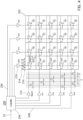
- Figure 4 depicts an array of individually controllable elements forming an electrode array 202.
- Figure 4 is a diagrammatic view of an exemplary driving system 200 for controlling droplet operation by an AM-EWoD propulsion electrode array 202.
- the AM-EWoD driving system 200 may be in the form of an integrated circuit adhered to a support plate.
- the elements of the EWoD device are arranged in the form of a matrix having a plurality of data lines and a plurality of gate lines. Each element of the matrix contains a TFT for controlling the electrode potential of a corresponding electrode, and each TFT is connected to one of the gate lines and one of the data lines.
- the electrode of the element is indicated as a capacitor Cp.
- the storage capacitor Cs is arranged in parallel with Cp and is not separately shown in Figure 4 .
- the controller shown comprises a microcontroller 204 including control logic and switching logic. It receives input data relating to droplet operations to be performed from the input data lines 22.
- the microcontroller has an output for each data line of the EWoD matrix, providing a data signal.
- a data signal line 206 connects each output to a data line of the matrix.
- the microcontroller also has an output for each gate line of the matrix, providing a gate line selection signal.
- a gate signal line 208 connects each output to a gate line of the matrix.
- a data line driver 210 and a gate line driver 212 is arranged in each data and gate signal line, respectively.
- the figure shows the signals lines only for those data lines and gate lines shown in the figure.
- the gate line drivers may be integrated in a single integrated circuit.
- the data line drivers may be integrated in a single integrated circuit.
- the integrated circuit may include the complete gate driver assembly together with the microcontroller.
- the integrated circuit may be integrated on a support plate of the AM-EWoD device.
- the integrated circuit may include the entire AM-EWoD device driving system.
- the data line drivers provide the signal levels corresponding to a droplet operation.
- the gate line drivers provide the signals for selecting the gate line of which the electrodes are to be actuated.
- a sequence of voltages of one of the data line drivers 210 is shown in Figure 4
- AM-EWoD cells use line-at-a-time addressing, in which one gate line n is high while all the others are low. The signals on all of the data lines are then transferred to all of the pixels in row n. At the end of the line time gate line n signal goes low and the next gate line n+1 goes high, so that data for the next line is transferred to the TFT pixels in row n+1. This continues with all of the gate lines being scanned sequentially so the whole matrix is driven. This is the same method that is used in almost all AM-LCDs, such as mobile phone screens, laptop screens and LC-TVs, whereby TFTs control the voltage maintained across the liquid crystal layer, and in AM-EPDs (electrophoretic displays).
- AM-LCDs such as mobile phone screens, laptop screens and LC-TVs
- Figure 5A depicts an array of elements on an AM-EWoD device without a conformal layer.
- a driving voltage has been applied to high ionic strength solutions and, as can be seen, results in damage and defects around the edge of some of the elements. An example is highlighted in a dotted line box.
- the result of this damage is failure of to perform EWoD actuation of an aqueous droplet in the area, further failure of an aqueous droplet to wet the area, and/or also general failures to dispense or split from an existing droplet to form two droplets.
- Figure 5B shows an array of elements, similar to those depicted in Figure 5A but coated in parylene C. Again, a driving voltage has been applied to high ionic strength droplets but did not result in the defects seen in Figure 5A .
- the result of the conformal coating is the lack of damage seen in Figure 5A resulting in the ability of an aqueous droplet to wet the area and/or dispense or split from an existing droplet to form two droplets in areas of an AM-EWoD device contacted by high ionic strength droplets.
- Solution 1 was left to stand for at least 2 hours to fully react and was used within 24 hours. Substrates were immersed in the Solution 1 for 30 minutes, while ensuring the flex strips of the TFT arrays were kept dry. Substrates were removed and air dried for 15 minutes and then cleaned in isopropanol for 15-30 seconds with agitation using tweezers. Substrates were dried with an air gun and stored in a Teflon box for Parylene C coating within 30 hours.
- the deposition zone remained at ambient temperature, circa 25°C, and around 50 milliTorr.
- the system was maintained at temperature and pressure for two hours.
- the system was allowed to return gradually to ambient temperature over 30-40 minutes before the stage and vacuum pump were turned off and the system vented.
- the samples were removed from the deposition chamber and the coating thickness verified as circa 100 nm by profilometry.
- Figure 6 depicts the reliable dispensation of a droplet through electrowetting actuation even after 22 hours of continuous operation (dispensing electrowetting actuation shown from Figure 6 top left to top middle to top right images), as opposed to an AM-EWoD device shown in Figure 5A . Even after this the droplet can be moved over the continuously actuated area (shown in Figure 6 bottom left to bottom middle to bottom right images).
- the invention can be used in a myriad of different applications.
- the invention can be used to move cells, nucleic acids, nucleic acid templates, proteins, initiation oligonucleotide sequences for nucleic acid synthesis, beads, magnetic beads, cells immobilised on magnetic beads, or biopolymers immobilised on magnetic beads.
- the steps of disposing an aqueous droplet having an ionic strength on a first matrix electrode and providing a differential electrical potential may be repeated many times. They may be repeated over 1000 times or over 10,000 times, sometimes over a 24 hour period.
- the present method can be used in the synthesis of nucleic acids, such as phosphoramidite-based nucleic acid synthesis, templated or non-templated enzymatic nucleic acid synthesis, or more specifically, terminal deoxynucleotidyl transferase (TdT) mediated addition of 3'-O-reversibly terminated nucleoside 5'-triphosphates to the 3'-end of 5'-immobilized nucleic acids.
- TdT terminal deoxynucleotidyl transferase
- the present method can be used in the preparation of oligonucleotide sequences, either via synthesis or assembly.
- the device allows synthesis and movement of defined sequences.
- the initiation sequences can be modified at a specific location above an electrode and the extended oligonucleotides prepared.
- the initiation sequences at different locations can be exposed to different nucleotides, thereby synthesising different sequences in different regions of the electrokinetic device.
- sequences After synthesis of a defined population of different sequences in different regions of the electrokinetic device, the sequences can be further assembled in longer contiguous sequences by joining two or more synthesised strands together.
- the steps of synthesis and assembly may involve high solute concentrations where the ionic strength would degrade the devices without the protecting conformal layer.
- the method of moving aqueous droplets may also be used to help facilitate cell-free expression of peptides or proteins.
- droplets containing a nucleic acid template and a cell-free system having components for protein expression in an oil-filled environment can be moved using a method of the invention in the described electrokinetic device.
- the present invention can be used to automate the movements of droplets in a cartridge.
- droplets intended for analysis can be moved according to the present invention.
- the present invention could be incorporated into a cartridge used for local clinician diagnostics.
- NAAT nucleic acid amplification testing
- it could be used in conjunction with nucleic acid amplification testing (NAAT) to determine nucleic acid targets in, for example, genetic testing for indications such as cancer biomarkers, pathogen testing for example detecting bacteria in a blood sample or virus detection, such as a coronavirus, e.g. SARS-CoV-2 for the diagnosis of COVID-19.
- NAAT nucleic acid amplification testing
- the device may be thermocycled to enable nucleic acid amplification, or the device may be held at a desired temperature for isothermal amplification. Having different sequences synthesised in different regions of the device allows multiplex amplification using different primers in different regions of the device.
- the invention can be used in conjunction with next generation sequencing in which DNA is synthesised by the addition of nucleotides and large numbers of samples are sequenced in parallel.
- the present invention can be used to accurately locate the individual samples used in next generation sequencing.
- the invention can be used to automate library preparation for next generation sequencing. For example the steps of ligation of sequencing adaptors can be carried out on the device. Amplification of a selective subset of sequences from a sample can then have adaptors attached to enable sequencing of the amplified population.
Landscapes
- Chemical & Material Sciences (AREA)
- Health & Medical Sciences (AREA)
- Dispersion Chemistry (AREA)
- Clinical Laboratory Science (AREA)
- General Health & Medical Sciences (AREA)
- Chemical Kinetics & Catalysis (AREA)
- Analytical Chemistry (AREA)
- Hematology (AREA)
- Fluid Mechanics (AREA)
- Physics & Mathematics (AREA)
- Life Sciences & Earth Sciences (AREA)
- Biochemistry (AREA)
- Molecular Biology (AREA)
- Apparatus Associated With Microorganisms And Enzymes (AREA)
- Measuring Or Testing Involving Enzymes Or Micro-Organisms (AREA)
- Preparation Of Compounds By Using Micro-Organisms (AREA)
Claims (15)
- Verfahren zum Bewegen eines wässrigen Tröpfchens (35), umfassend:
Bereitstellen einer elektrokinetischen Vorrichtung, die Folgendes beinhaltet:
ein erstes Substrat (10), das eine Matrix von Elektroden (11) aufweist, wobei jede der Matrixelektroden mit einem Dünnfilmtransistor gekoppelt ist und wobei die Matrixelektroden mit einer Funktionsbeschichtung überzogen sind, umfassend:eine dielektrische Schicht (12), die mehrere Schichten von Materialien, die ausgewählt sind aus Siliziumnitrid, Hafniumoxid oder Aluminiumoxid, umfasst, in Kontakt mit den Matrixelektroden,eine konforme Schicht (30), die Parylen umfasst, in Kontakt mit der dielektrischen Schicht, undeine hydrophobe Schicht (13) in Kontakt mit der konformen Schicht, wobei das Parylen fungiert alseine Schutzbeschichtung zwischen der dielektrischen Schicht und der hydrophoben Schicht;ein zweites Substrat, das eine obere Elektrode (14) umfasst, wobei das zweite Substrat ferner eine zweite hydrophobe Schicht umfasst, die auf der zweiten Elektrode angeordnet ist;einen Abstandshalter (15), der zwischen dem ersten Substrat und dem zweiten Substrat angeordnet ist und einen elektrokinetischen Arbeitsraum zwischen den hydrophoben Schichten definiert; undeine Spannungsquelle, die betriebsfähig mit den Matrixelektroden gekoppelt ist;Bereitstellen eines wässrigen Tröpfchens auf einer ersten Matrixelektrode; undBereitstellen eines elektrischen Differenzpotentials zwischen der ersten Matrixelektrode und einer zweiten Matrixelektrode mit der Spannungsquelle, wodurch das wässrige Tröpfchen zwischen der ersten Matrixelektrode und der zweiten Matrixelektrode bewegt wird. - Verfahren nach Anspruch 1, wobei das wässrige Tröpfchen eine Ionenstärke aufweist, die größer als 0,1 M ist.
- Verfahren nach Anspruch 1 oder 2, wobei das wässrige Tröpfchen eine Ionenstärke aufweist, die größer als 1,0 M ist.
- Verfahren nach einem der vorhergehenden Ansprüche, wobei die dielektrische Schicht zwischen 10 nm und 100 µm dick ist.
- Verfahren nach einem der vorhergehenden Ansprüche, wobei die geschichtete Dielektrik Folgendes umfasst:eine erste Schicht, die ein Aluminiumoxid oder ein Hafniumoxid beinhaltet, wobei die erste Schicht eine Dicke zwischen 9 nm und 80 nm aufweist;eine zweite Schicht, die ein Tantalumoxid oder ein Hafniumoxid beinhaltet, wobei die zweite Schicht eine Dicke zwischen 40 nm und 250 nm aufweist; undeine dritte Schicht, die ein Tantalumoxid oder ein Hafniumoxid beinhaltet, wobei die dritte Schicht eine Dicke zwischen 5 nm und 60 nm aufweist; wobei die zweite Schicht zwischen der ersten und der dritten Schicht angeordnet ist.
- Verfahren nach einem der vorhergehenden Ansprüche, wobei die konforme Schicht, die Parylen umfasst, circa 100 nm dick ist.
- Verfahren nach einem der vorhergehenden Ansprüche, wobei die hydrophobe Schicht eine Fluorpolymerbeschichtung, eine fluorinierte Silanbeschichtung, einen Manganoxid-Polystyrol-Nano-Verbundwerkstoff, einen Zinkoxid-Polystyrol-Nano-Verbundwerkstoff, ausgefallenes Calciumcarbonat, eine Kohlenstoff-Nanoröhren-Struktur, eine Siliciumdioxid-Nanobeschichtung oder eine mit einer rutschigen Flüssigkeit angereicherte poröse Beschichtung umfasst.
- Verfahren nach einem der vorhergehenden Ansprüche, wobei die Funktionsbeschichtung eine dielektrische Schicht, die Siliziumnitrid umfasst, eine konforme Schicht, die Parylen umfasst, und eine hydrophobe Schicht, die ein amorphes Fluorpolymer umfasst, beinhaltet.
- Verfahren nach einem der vorhergehenden Ansprüche, wobei die elektrokinetische Vorrichtung ferner eine Steuerung beinhaltet, um eine Spannung, die den einzelnen Matrixelektroden bereitgestellt wird, zu regeln.
- Verfahren nach Anspruch 9, wobei die elektrokinetische Vorrichtung ferner eine Vielzahl von Abtastleitungen und eine Vielzahl von Gate-Leitungen beinhaltet, wobei jeder der Dünnfilmtransistoren mit einer Abtastleitung und einer Gate-Leitung gekoppelt ist, und die Vielzahl von Gate-Leitungen betriebsfähig mit der Steuerung verbunden sind.
- Verfahren nach einem der vorhergehenden Ansprüche, wobei das wässrige Tröpfchen ein Volumen von 1 µl oder kleiner aufweist.
- Verfahren nach einem der vorhergehenden Ansprüche, ferner umfassend:Anordnen eines zweiten wässrigen Tröpfchens auf einer dritten Matrixelektrode; undBereitstellen eines elektrischen Differenzpotentials zwischen der dritten Matrixelektrode und der zweiten Matrixelektrode mit der Spannungsquelle, wodurch das wässrige Tröpfchen mit dem zweiten wässrigen Tröpfchen in Kontakt gebracht wird.
- Verfahren nach einem der Ansprüche 1 bis 12 zum Durchführen einer tröpfchenbasierten Nukleinsäuresynthese, einer tröpfchenbasierten Nukleinsäureamplifikation oder eines tröpfchenbasierten Nukleinsäureaufbaus, wobei das Verfahren das Wiederholen des Verfahrens nach einem der Ansprüche 1 bis 12 umfasst, um Nukleotide zu einem Startoligonukleotid hinzuzufügen oder zwei oder mehr Nukleinsäurestränge in einem oder mehreren Tröpfchen zusammenzufügen.
- Verfahren nach einem der Ansprüche 1 bis 12 zum Durchführen einer tröpfchenbasierten zellfreien Expression von Peptiden oder Proteinen, wobei das Verfahren das Wiederholen des Verfahrens nach einem der Ansprüche 1 bis 12 umfasst, wobei die Tröpfchen Nukleinsäurevorlagen und ein zellfreies System, das Komponenten für eine Proteinexpression aufweist, enthalten.
- Verfahren nach einem der Ansprüche 13 oder 14, wobei das wässrige Tröpfchen zwischen der ersten Matrixelektrode und der zweiten Matrixelektrode mehr als 1000 Mal bewegt wird.
Applications Claiming Priority (2)
| Application Number | Priority Date | Filing Date | Title |
|---|---|---|---|
| GBGB2005399.7A GB202005399D0 (en) | 2020-04-14 | 2020-04-14 | A method of electrowetting |
| PCT/GB2021/050896 WO2021209751A1 (en) | 2020-04-14 | 2021-04-14 | A method of electrowetting |
Publications (4)
| Publication Number | Publication Date |
|---|---|
| EP4135896A1 EP4135896A1 (de) | 2023-02-22 |
| EP4135896C0 EP4135896C0 (de) | 2025-01-15 |
| EP4135896B1 true EP4135896B1 (de) | 2025-01-15 |
| EP4135896B8 EP4135896B8 (de) | 2025-02-26 |
Family
ID=70848148
Family Applications (1)
| Application Number | Title | Priority Date | Filing Date |
|---|---|---|---|
| EP21721585.4A Active EP4135896B8 (de) | 2020-04-14 | 2021-04-14 | Verfahren zur elektrobenetzung |
Country Status (8)
| Country | Link |
|---|---|
| US (2) | US20230372939A1 (de) |
| EP (1) | EP4135896B8 (de) |
| JP (1) | JP2023521833A (de) |
| KR (1) | KR20220167287A (de) |
| CN (1) | CN115485069A (de) |
| GB (2) | GB202005399D0 (de) |
| TW (1) | TWI885127B (de) |
| WO (1) | WO2021209751A1 (de) |
Family Cites Families (23)
| Publication number | Priority date | Publication date | Assignee | Title |
|---|---|---|---|---|
| US20080169197A1 (en) * | 2004-10-18 | 2008-07-17 | Stratos Biosystems, Llc | Single-Sided Apparatus For Manipulating Droplets By Electrowetting-On-Dielectric Techniques |
| US20070023292A1 (en) * | 2005-07-26 | 2007-02-01 | The Regents Of The University Of California | Small object moving on printed circuit board |
| EP1816491A1 (de) * | 2006-02-01 | 2007-08-08 | Varioptic | Elektrowettingvorrichtung |
| US7791815B2 (en) * | 2007-03-13 | 2010-09-07 | Varioptic S.A. | Dielectric coatings for electrowetting applications |
| JP2010107908A (ja) * | 2008-10-31 | 2010-05-13 | Sony Corp | エレクトロウェッティング装置、可変焦点レンズ、光ピックアップ装置、光記録再生装置、液滴操作装置、光学素子、ズームレンズ、撮像装置、光変調装置、表示装置、ストロボ装置及びエレクトロウェッティング装置の駆動方法 |
| US20110140996A1 (en) * | 2009-12-15 | 2011-06-16 | Lesley Anne Parry-Jones | Switchable transmissive/reflective electrowetting display |
| WO2012003303A2 (en) * | 2010-06-30 | 2012-01-05 | University Of Cincinnati | Electrowetting devices on flat and flexible paper substrates |
| CN102671722B (zh) * | 2011-02-17 | 2015-03-11 | 王崇智 | 基于微电极阵列结构的现场可编程芯片实验室 |
| JP2013037219A (ja) * | 2011-08-09 | 2013-02-21 | Sony Corp | 光学素子、光学素子アレイ、表示装置および電子機器 |
| US20140378339A1 (en) * | 2012-01-24 | 2014-12-25 | Katholieke Universiteit Euven | Patterning device |
| US9630183B2 (en) * | 2012-02-01 | 2017-04-25 | Wayne State University | Electrowetting on dielectric using graphene |
| US9297998B2 (en) * | 2014-03-28 | 2016-03-29 | Amazon Technologies, Inc. | Electrode of an electrowetting device |
| EP2975446A1 (de) * | 2014-07-16 | 2016-01-20 | Parrot | Flüssiglinsen mit geringer hysterese der optischen leistung |
| TWI698282B (zh) * | 2014-12-05 | 2020-07-11 | 加州大學董事會 | 基板、微流體元件、移動微流體元件中的液滴之方法以及用於操控微流體元件中的液滴之程序 |
| US9751083B2 (en) | 2015-04-07 | 2017-09-05 | University Of Macau | Electronic module for real-time droplet-position sensing and driving in digital microfluidic system |
| CN114643087A (zh) * | 2017-04-26 | 2022-06-21 | 伯克利之光生命科技公司 | 使用具有优化电润湿表面的微流体装置的生物处理系统和方法 |
| US10695761B2 (en) * | 2017-05-30 | 2020-06-30 | Sharp Life Science (Eu) Limited | Microfluidic device with multiple temperature zones and enhanced temperature control |
| CA3075408C (en) | 2017-10-18 | 2022-06-28 | E Ink Corporation | Digital microfluidic devices including dual substrates with thin-film transistors and capacitive sensing |
| US20190262829A1 (en) * | 2018-02-28 | 2019-08-29 | Volta Labs, Inc. | Directing Motion of Droplets Using Differential Wetting |
| US10859813B2 (en) * | 2018-07-03 | 2020-12-08 | Sharp Life Science (Eu) Limited | Optically black AM-EWOD array element structure |
| KR102921120B1 (ko) | 2019-05-03 | 2026-01-30 | 이 잉크 코포레이션 | 액티브 매트릭스 백플레인들과의 사용을 위한 고 유전상수를 갖는 층상 구조 |
| US11554374B2 (en) * | 2020-01-17 | 2023-01-17 | Nuclera Nucleics Ltd. | Spatially variable dielectric layers for digital microfluidics |
| GB202002077D0 (en) * | 2020-02-14 | 2020-04-01 | Nuclera Nucleics Ltd | Methods for cell-free protein expression |
-
2020
- 2020-04-14 GB GBGB2005399.7A patent/GB202005399D0/en not_active Ceased
-
2021
- 2021-04-14 WO PCT/GB2021/050896 patent/WO2021209751A1/en not_active Ceased
- 2021-04-14 KR KR1020227035751A patent/KR20220167287A/ko active Pending
- 2021-04-14 TW TW110113478A patent/TWI885127B/zh active
- 2021-04-14 EP EP21721585.4A patent/EP4135896B8/de active Active
- 2021-04-14 CN CN202180027240.9A patent/CN115485069A/zh active Pending
- 2021-04-14 JP JP2022562316A patent/JP2023521833A/ja active Pending
- 2021-04-14 US US17/918,871 patent/US20230372939A1/en active Pending
- 2021-04-14 GB GB2215444.7A patent/GB2609145B/en active Active
-
2022
- 2022-10-13 US US17/965,750 patent/US11806715B2/en active Active
Also Published As
| Publication number | Publication date |
|---|---|
| GB2609145B (en) | 2025-01-01 |
| EP4135896C0 (de) | 2025-01-15 |
| US20230057330A1 (en) | 2023-02-23 |
| KR20220167287A (ko) | 2022-12-20 |
| WO2021209751A1 (en) | 2021-10-21 |
| GB202215444D0 (en) | 2022-11-30 |
| US20230372939A1 (en) | 2023-11-23 |
| EP4135896B8 (de) | 2025-02-26 |
| JP2023521833A (ja) | 2023-05-25 |
| CN115485069A (zh) | 2022-12-16 |
| EP4135896A1 (de) | 2023-02-22 |
| TW202204041A (zh) | 2022-02-01 |
| GB202005399D0 (en) | 2020-05-27 |
| US11806715B2 (en) | 2023-11-07 |
| TWI885127B (zh) | 2025-06-01 |
| GB2609145A (en) | 2023-01-25 |
Similar Documents
| Publication | Publication Date | Title |
|---|---|---|
| AU2021220690B2 (en) | Methods for cell-free protein expression | |
| US20240359181A1 (en) | Methods and compositions for improved biomolecule assays on digital microfluidic devices | |
| WO2022096882A1 (en) | Dielectric layers for digital microfluidic devices | |
| CN115884828A (zh) | 在数字微流体装置中用于延长的液滴保持的间歇驱动模式 | |
| WO2023285821A1 (en) | A method of forming arrays of droplets | |
| WO2023079310A1 (en) | Protein purification using a digital microfluidic device | |
| US20230042211A1 (en) | Methods for cell-free protein expression | |
| US20240352451A1 (en) | A method of loading devices using electrowetting | |
| EP4135896B1 (de) | Verfahren zur elektrobenetzung | |
| US20250196132A1 (en) | Loading and formation of multiple reservoirs | |
| US20250214081A1 (en) | Controlled reservoir filling | |
| EP4544300A1 (de) | Proteinbindungstests | |
| TWI797601B (zh) | 數位微流控裝置及驅動數位微流控系統之方法 | |
| EP4565914A1 (de) | Verfahren zur bildung von tröpfchenarrays | |
| WO2025003668A1 (en) | Protein binding assays | |
| WO2025253020A2 (en) | Assays on expressed proteins | |
| WO2024149996A1 (en) | Protein expression systems | |
| EP4543591A1 (de) | Gesteuerte reservoirbefüllung |
Legal Events
| Date | Code | Title | Description |
|---|---|---|---|
| STAA | Information on the status of an ep patent application or granted ep patent |
Free format text: STATUS: UNKNOWN |
|
| STAA | Information on the status of an ep patent application or granted ep patent |
Free format text: STATUS: THE INTERNATIONAL PUBLICATION HAS BEEN MADE |
|
| PUAI | Public reference made under article 153(3) epc to a published international application that has entered the european phase |
Free format text: ORIGINAL CODE: 0009012 |
|
| STAA | Information on the status of an ep patent application or granted ep patent |
Free format text: STATUS: REQUEST FOR EXAMINATION WAS MADE |
|
| 17P | Request for examination filed |
Effective date: 20221104 |
|
| AK | Designated contracting states |
Kind code of ref document: A1 Designated state(s): AL AT BE BG CH CY CZ DE DK EE ES FI FR GB GR HR HU IE IS IT LI LT LU LV MC MK MT NL NO PL PT RO RS SE SI SK SM TR |
|
| RAP3 | Party data changed (applicant data changed or rights of an application transferred) |
Owner name: NUCLERA NUCLEICS LTD |
|
| RIN1 | Information on inventor provided before grant (corrected) |
Inventor name: THE OTHER INVENTORS HAVE WAIVED THEIR RIGHT TO BE THUS MENTIONED. Inventor name: VISANI, CRISTINA Inventor name: PAOLINI, RICK Inventor name: SLOMINSKI, LUKE Inventor name: ZHITOMIRSKY, DAVID Inventor name: MCINROY, GORDON ROSS Inventor name: KALSI, SUMIT Inventor name: CHEN, MICHAEL CHUN HAO |
|
| RAP3 | Party data changed (applicant data changed or rights of an application transferred) |
Owner name: NUCLERA LTD |
|
| DAV | Request for validation of the european patent (deleted) | ||
| DAX | Request for extension of the european patent (deleted) | ||
| GRAP | Despatch of communication of intention to grant a patent |
Free format text: ORIGINAL CODE: EPIDOSNIGR1 |
|
| STAA | Information on the status of an ep patent application or granted ep patent |
Free format text: STATUS: GRANT OF PATENT IS INTENDED |
|
| INTG | Intention to grant announced |
Effective date: 20240813 |
|
| RIN1 | Information on inventor provided before grant (corrected) |
Inventor name: THE OTHER INVENTOR HAS WAIVED HIS RIGHT TO BE THUS MENTIONED. Inventor name: VISANI, CRISTINA Inventor name: PAOLINI, RICK Inventor name: SLOMINSKI, LUKE Inventor name: ZHITOMIRSKY, DAVID Inventor name: MCINROY, GORDON ROSS Inventor name: KALSI, SUMIT Inventor name: CHEN, MICHAEL CHUN HAO |
|
| GRAS | Grant fee paid |
Free format text: ORIGINAL CODE: EPIDOSNIGR3 |
|
| GRAA | (expected) grant |
Free format text: ORIGINAL CODE: 0009210 |
|
| STAA | Information on the status of an ep patent application or granted ep patent |
Free format text: STATUS: THE PATENT HAS BEEN GRANTED |
|
| AK | Designated contracting states |
Kind code of ref document: B1 Designated state(s): AL AT BE BG CH CY CZ DE DK EE ES FI FR GB GR HR HU IE IS IT LI LT LU LV MC MK MT NL NO PL PT RO RS SE SI SK SM TR |
|
| REG | Reference to a national code |
Ref country code: CH Ref legal event code: EP Ref country code: GB Ref legal event code: FG4D |
|
| RIN2 | Information on inventor provided after grant (corrected) |
Inventor name: VISANI, CRISTINA Inventor name: PAOLINI, RICK Inventor name: SLOMINSKI, LUKE Inventor name: ZHITOMIRSKY, DAVID Inventor name: MCINROY, GORDON ROSS Inventor name: BELL, LAURENCE LIVINGSTONE Inventor name: KALSI, SUMIT Inventor name: CHEN, MICHAEL CHUN HAO |
|
| REG | Reference to a national code |
Ref country code: DE Ref legal event code: R096 Ref document number: 602021024970 Country of ref document: DE |
|
| REG | Reference to a national code |
Ref country code: CH Ref legal event code: PK Free format text: BERICHTIGUNG B8 |
|
| REG | Reference to a national code |
Ref country code: IE Ref legal event code: FG4D |
|
| U01 | Request for unitary effect filed |
Effective date: 20250203 |
|
| U07 | Unitary effect registered |
Designated state(s): AT BE BG DE DK EE FI FR IT LT LU LV MT NL PT RO SE SI Effective date: 20250207 |
|
| U20 | Renewal fee for the european patent with unitary effect paid |
Year of fee payment: 5 Effective date: 20250421 |
|
| PG25 | Lapsed in a contracting state [announced via postgrant information from national office to epo] |
Ref country code: RS Free format text: LAPSE BECAUSE OF FAILURE TO SUBMIT A TRANSLATION OF THE DESCRIPTION OR TO PAY THE FEE WITHIN THE PRESCRIBED TIME-LIMIT Effective date: 20250415 |
|
| PG25 | Lapsed in a contracting state [announced via postgrant information from national office to epo] |
Ref country code: PL Free format text: LAPSE BECAUSE OF FAILURE TO SUBMIT A TRANSLATION OF THE DESCRIPTION OR TO PAY THE FEE WITHIN THE PRESCRIBED TIME-LIMIT Effective date: 20250115 |
|
| PG25 | Lapsed in a contracting state [announced via postgrant information from national office to epo] |
Ref country code: ES Free format text: LAPSE BECAUSE OF FAILURE TO SUBMIT A TRANSLATION OF THE DESCRIPTION OR TO PAY THE FEE WITHIN THE PRESCRIBED TIME-LIMIT Effective date: 20250115 |
|
| PGFP | Annual fee paid to national office [announced via postgrant information from national office to epo] |
Ref country code: GB Payment date: 20250423 Year of fee payment: 5 |
|
| PG25 | Lapsed in a contracting state [announced via postgrant information from national office to epo] |
Ref country code: NO Free format text: LAPSE BECAUSE OF FAILURE TO SUBMIT A TRANSLATION OF THE DESCRIPTION OR TO PAY THE FEE WITHIN THE PRESCRIBED TIME-LIMIT Effective date: 20250415 Ref country code: IS Free format text: LAPSE BECAUSE OF FAILURE TO SUBMIT A TRANSLATION OF THE DESCRIPTION OR TO PAY THE FEE WITHIN THE PRESCRIBED TIME-LIMIT Effective date: 20250515 |
|
| PG25 | Lapsed in a contracting state [announced via postgrant information from national office to epo] |
Ref country code: HR Free format text: LAPSE BECAUSE OF FAILURE TO SUBMIT A TRANSLATION OF THE DESCRIPTION OR TO PAY THE FEE WITHIN THE PRESCRIBED TIME-LIMIT Effective date: 20250115 |
|
| PGFP | Annual fee paid to national office [announced via postgrant information from national office to epo] |
Ref country code: CH Payment date: 20250501 Year of fee payment: 5 |
|
| PG25 | Lapsed in a contracting state [announced via postgrant information from national office to epo] |
Ref country code: SM Free format text: LAPSE BECAUSE OF FAILURE TO SUBMIT A TRANSLATION OF THE DESCRIPTION OR TO PAY THE FEE WITHIN THE PRESCRIBED TIME-LIMIT Effective date: 20250115 |
|
| PG25 | Lapsed in a contracting state [announced via postgrant information from national office to epo] |
Ref country code: CZ Free format text: LAPSE BECAUSE OF FAILURE TO SUBMIT A TRANSLATION OF THE DESCRIPTION OR TO PAY THE FEE WITHIN THE PRESCRIBED TIME-LIMIT Effective date: 20250115 |
|
| PG25 | Lapsed in a contracting state [announced via postgrant information from national office to epo] |
Ref country code: SK Free format text: LAPSE BECAUSE OF FAILURE TO SUBMIT A TRANSLATION OF THE DESCRIPTION OR TO PAY THE FEE WITHIN THE PRESCRIBED TIME-LIMIT Effective date: 20250115 |
|
| PLBE | No opposition filed within time limit |
Free format text: ORIGINAL CODE: 0009261 |
|
| STAA | Information on the status of an ep patent application or granted ep patent |
Free format text: STATUS: NO OPPOSITION FILED WITHIN TIME LIMIT |
|
| PG25 | Lapsed in a contracting state [announced via postgrant information from national office to epo] |
Ref country code: MC Free format text: LAPSE BECAUSE OF FAILURE TO SUBMIT A TRANSLATION OF THE DESCRIPTION OR TO PAY THE FEE WITHIN THE PRESCRIBED TIME-LIMIT Effective date: 20250115 |
|
| 26N | No opposition filed |
Effective date: 20251016 |