EP4135011A1 - Thin film deposition method and semiconductor device - Google Patents
Thin film deposition method and semiconductor device Download PDFInfo
- Publication number
- EP4135011A1 EP4135011A1 EP21928347.0A EP21928347A EP4135011A1 EP 4135011 A1 EP4135011 A1 EP 4135011A1 EP 21928347 A EP21928347 A EP 21928347A EP 4135011 A1 EP4135011 A1 EP 4135011A1
- Authority
- EP
- European Patent Office
- Prior art keywords
- thin
- layer
- film deposition
- deposited layer
- film
- Prior art date
- Legal status (The legal status is an assumption and is not a legal conclusion. Google has not performed a legal analysis and makes no representation as to the accuracy of the status listed.)
- Pending
Links
Images



Classifications
-
- H—ELECTRICITY
- H10—SEMICONDUCTOR DEVICES; ELECTRIC SOLID-STATE DEVICES NOT OTHERWISE PROVIDED FOR
- H10D—INORGANIC ELECTRIC SEMICONDUCTOR DEVICES
- H10D64/00—Electrodes of devices having potential barriers
- H10D64/01—Manufacture or treatment
- H10D64/013—Manufacture or treatment of electrodes having a conductor capacitively coupled to a semiconductor by an insulator
- H10D64/01302—Manufacture or treatment of electrodes having a conductor capacitively coupled to a semiconductor by an insulator the insulator being formed after the semiconductor body, the semiconductor being silicon
- H10D64/01354—Manufacture or treatment of electrodes having a conductor capacitively coupled to a semiconductor by an insulator the insulator being formed after the semiconductor body, the semiconductor being silicon passivation or protection of the electrode, e.g. using re-oxidation
-
- H—ELECTRICITY
- H10—SEMICONDUCTOR DEVICES; ELECTRIC SOLID-STATE DEVICES NOT OTHERWISE PROVIDED FOR
- H10P—GENERIC PROCESSES OR APPARATUS FOR THE MANUFACTURE OR TREATMENT OF DEVICES COVERED BY CLASS H10
- H10P14/00—Formation of materials, e.g. in the shape of layers or pillars
- H10P14/60—Formation of materials, e.g. in the shape of layers or pillars of insulating materials
- H10P14/63—Formation of materials, e.g. in the shape of layers or pillars of insulating materials characterised by the formation processes
- H10P14/6326—Deposition processes
- H10P14/6328—Deposition from the gas or vapour phase
- H10P14/6334—Deposition from the gas or vapour phase using decomposition or reaction of gaseous or vapour phase compounds, i.e. chemical vapour deposition
- H10P14/6336—Deposition from the gas or vapour phase using decomposition or reaction of gaseous or vapour phase compounds, i.e. chemical vapour deposition in the presence of a plasma [PECVD]
-
- C—CHEMISTRY; METALLURGY
- C23—COATING METALLIC MATERIAL; COATING MATERIAL WITH METALLIC MATERIAL; CHEMICAL SURFACE TREATMENT; DIFFUSION TREATMENT OF METALLIC MATERIAL; COATING BY VACUUM EVAPORATION, BY SPUTTERING, BY ION IMPLANTATION OR BY CHEMICAL VAPOUR DEPOSITION, IN GENERAL; INHIBITING CORROSION OF METALLIC MATERIAL OR INCRUSTATION IN GENERAL
- C23C—COATING METALLIC MATERIAL; COATING MATERIAL WITH METALLIC MATERIAL; SURFACE TREATMENT OF METALLIC MATERIAL BY DIFFUSION INTO THE SURFACE, BY CHEMICAL CONVERSION OR SUBSTITUTION; COATING BY VACUUM EVAPORATION, BY SPUTTERING, BY ION IMPLANTATION OR BY CHEMICAL VAPOUR DEPOSITION, IN GENERAL
- C23C16/00—Chemical coating by decomposition of gaseous compounds, without leaving reaction products of surface material in the coating, i.e. chemical vapour deposition [CVD] processes
- C23C16/22—Chemical coating by decomposition of gaseous compounds, without leaving reaction products of surface material in the coating, i.e. chemical vapour deposition [CVD] processes characterised by the deposition of inorganic material, other than metallic material
- C23C16/30—Deposition of compounds, mixtures or solid solutions, e.g. borides, carbides, nitrides
- C23C16/34—Nitrides
- C23C16/345—Silicon nitride
-
- C—CHEMISTRY; METALLURGY
- C23—COATING METALLIC MATERIAL; COATING MATERIAL WITH METALLIC MATERIAL; CHEMICAL SURFACE TREATMENT; DIFFUSION TREATMENT OF METALLIC MATERIAL; COATING BY VACUUM EVAPORATION, BY SPUTTERING, BY ION IMPLANTATION OR BY CHEMICAL VAPOUR DEPOSITION, IN GENERAL; INHIBITING CORROSION OF METALLIC MATERIAL OR INCRUSTATION IN GENERAL
- C23C—COATING METALLIC MATERIAL; COATING MATERIAL WITH METALLIC MATERIAL; SURFACE TREATMENT OF METALLIC MATERIAL BY DIFFUSION INTO THE SURFACE, BY CHEMICAL CONVERSION OR SUBSTITUTION; COATING BY VACUUM EVAPORATION, BY SPUTTERING, BY ION IMPLANTATION OR BY CHEMICAL VAPOUR DEPOSITION, IN GENERAL
- C23C16/00—Chemical coating by decomposition of gaseous compounds, without leaving reaction products of surface material in the coating, i.e. chemical vapour deposition [CVD] processes
- C23C16/44—Chemical coating by decomposition of gaseous compounds, without leaving reaction products of surface material in the coating, i.e. chemical vapour deposition [CVD] processes characterised by the method of coating
- C23C16/4401—Means for minimising impurities, e.g. dust, moisture or residual gas, in the reaction chamber
-
- C—CHEMISTRY; METALLURGY
- C23—COATING METALLIC MATERIAL; COATING MATERIAL WITH METALLIC MATERIAL; CHEMICAL SURFACE TREATMENT; DIFFUSION TREATMENT OF METALLIC MATERIAL; COATING BY VACUUM EVAPORATION, BY SPUTTERING, BY ION IMPLANTATION OR BY CHEMICAL VAPOUR DEPOSITION, IN GENERAL; INHIBITING CORROSION OF METALLIC MATERIAL OR INCRUSTATION IN GENERAL
- C23C—COATING METALLIC MATERIAL; COATING MATERIAL WITH METALLIC MATERIAL; SURFACE TREATMENT OF METALLIC MATERIAL BY DIFFUSION INTO THE SURFACE, BY CHEMICAL CONVERSION OR SUBSTITUTION; COATING BY VACUUM EVAPORATION, BY SPUTTERING, BY ION IMPLANTATION OR BY CHEMICAL VAPOUR DEPOSITION, IN GENERAL
- C23C16/00—Chemical coating by decomposition of gaseous compounds, without leaving reaction products of surface material in the coating, i.e. chemical vapour deposition [CVD] processes
- C23C16/44—Chemical coating by decomposition of gaseous compounds, without leaving reaction products of surface material in the coating, i.e. chemical vapour deposition [CVD] processes characterised by the method of coating
- C23C16/4401—Means for minimising impurities, e.g. dust, moisture or residual gas, in the reaction chamber
- C23C16/4408—Means for minimising impurities, e.g. dust, moisture or residual gas, in the reaction chamber by purging residual gases from the reaction chamber or gas lines
-
- C—CHEMISTRY; METALLURGY
- C23—COATING METALLIC MATERIAL; COATING MATERIAL WITH METALLIC MATERIAL; CHEMICAL SURFACE TREATMENT; DIFFUSION TREATMENT OF METALLIC MATERIAL; COATING BY VACUUM EVAPORATION, BY SPUTTERING, BY ION IMPLANTATION OR BY CHEMICAL VAPOUR DEPOSITION, IN GENERAL; INHIBITING CORROSION OF METALLIC MATERIAL OR INCRUSTATION IN GENERAL
- C23C—COATING METALLIC MATERIAL; COATING MATERIAL WITH METALLIC MATERIAL; SURFACE TREATMENT OF METALLIC MATERIAL BY DIFFUSION INTO THE SURFACE, BY CHEMICAL CONVERSION OR SUBSTITUTION; COATING BY VACUUM EVAPORATION, BY SPUTTERING, BY ION IMPLANTATION OR BY CHEMICAL VAPOUR DEPOSITION, IN GENERAL
- C23C16/00—Chemical coating by decomposition of gaseous compounds, without leaving reaction products of surface material in the coating, i.e. chemical vapour deposition [CVD] processes
- C23C16/44—Chemical coating by decomposition of gaseous compounds, without leaving reaction products of surface material in the coating, i.e. chemical vapour deposition [CVD] processes characterised by the method of coating
- C23C16/455—Chemical coating by decomposition of gaseous compounds, without leaving reaction products of surface material in the coating, i.e. chemical vapour deposition [CVD] processes characterised by the method of coating characterised by the method used for introducing gases into reaction chamber or for modifying gas flows in reaction chamber
- C23C16/45523—Pulsed gas flow or change of composition over time
- C23C16/45525—Atomic layer deposition [ALD]
- C23C16/45527—Atomic layer deposition [ALD] characterized by the ALD cycle, e.g. different flows or temperatures during half-reactions, unusual pulsing sequence, use of precursor mixtures or auxiliary reactants or activations
- C23C16/45536—Use of plasma, radiation or electromagnetic fields
-
- C—CHEMISTRY; METALLURGY
- C23—COATING METALLIC MATERIAL; COATING MATERIAL WITH METALLIC MATERIAL; CHEMICAL SURFACE TREATMENT; DIFFUSION TREATMENT OF METALLIC MATERIAL; COATING BY VACUUM EVAPORATION, BY SPUTTERING, BY ION IMPLANTATION OR BY CHEMICAL VAPOUR DEPOSITION, IN GENERAL; INHIBITING CORROSION OF METALLIC MATERIAL OR INCRUSTATION IN GENERAL
- C23C—COATING METALLIC MATERIAL; COATING MATERIAL WITH METALLIC MATERIAL; SURFACE TREATMENT OF METALLIC MATERIAL BY DIFFUSION INTO THE SURFACE, BY CHEMICAL CONVERSION OR SUBSTITUTION; COATING BY VACUUM EVAPORATION, BY SPUTTERING, BY ION IMPLANTATION OR BY CHEMICAL VAPOUR DEPOSITION, IN GENERAL
- C23C16/00—Chemical coating by decomposition of gaseous compounds, without leaving reaction products of surface material in the coating, i.e. chemical vapour deposition [CVD] processes
- C23C16/44—Chemical coating by decomposition of gaseous compounds, without leaving reaction products of surface material in the coating, i.e. chemical vapour deposition [CVD] processes characterised by the method of coating
- C23C16/50—Chemical coating by decomposition of gaseous compounds, without leaving reaction products of surface material in the coating, i.e. chemical vapour deposition [CVD] processes characterised by the method of coating using electric discharges
-
- C—CHEMISTRY; METALLURGY
- C23—COATING METALLIC MATERIAL; COATING MATERIAL WITH METALLIC MATERIAL; CHEMICAL SURFACE TREATMENT; DIFFUSION TREATMENT OF METALLIC MATERIAL; COATING BY VACUUM EVAPORATION, BY SPUTTERING, BY ION IMPLANTATION OR BY CHEMICAL VAPOUR DEPOSITION, IN GENERAL; INHIBITING CORROSION OF METALLIC MATERIAL OR INCRUSTATION IN GENERAL
- C23C—COATING METALLIC MATERIAL; COATING MATERIAL WITH METALLIC MATERIAL; SURFACE TREATMENT OF METALLIC MATERIAL BY DIFFUSION INTO THE SURFACE, BY CHEMICAL CONVERSION OR SUBSTITUTION; COATING BY VACUUM EVAPORATION, BY SPUTTERING, BY ION IMPLANTATION OR BY CHEMICAL VAPOUR DEPOSITION, IN GENERAL
- C23C16/00—Chemical coating by decomposition of gaseous compounds, without leaving reaction products of surface material in the coating, i.e. chemical vapour deposition [CVD] processes
- C23C16/56—After-treatment
-
- H—ELECTRICITY
- H01—ELECTRIC ELEMENTS
- H01J—ELECTRIC DISCHARGE TUBES OR DISCHARGE LAMPS
- H01J37/00—Discharge tubes with provision for introducing objects or material to be exposed to the discharge, e.g. for the purpose of examination or processing thereof
- H01J37/32—Gas-filled discharge tubes
- H01J37/36—Gas-filled discharge tubes for cleaning surfaces while plating with ions of materials introduced into the discharge, e.g. introduced by evaporation
-
- H—ELECTRICITY
- H10—SEMICONDUCTOR DEVICES; ELECTRIC SOLID-STATE DEVICES NOT OTHERWISE PROVIDED FOR
- H10D—INORGANIC ELECTRIC SEMICONDUCTOR DEVICES
- H10D64/00—Electrodes of devices having potential barriers
- H10D64/60—Electrodes characterised by their materials
- H10D64/66—Electrodes having a conductor capacitively coupled to a semiconductor by an insulator, e.g. MIS electrodes
- H10D64/68—Electrodes having a conductor capacitively coupled to a semiconductor by an insulator, e.g. MIS electrodes characterised by the insulator, e.g. by the gate insulator
- H10D64/693—Electrodes having a conductor capacitively coupled to a semiconductor by an insulator, e.g. MIS electrodes characterised by the insulator, e.g. by the gate insulator the insulator comprising nitrogen, e.g. nitrides, oxynitrides or nitrogen-doped materials
-
- H—ELECTRICITY
- H10—SEMICONDUCTOR DEVICES; ELECTRIC SOLID-STATE DEVICES NOT OTHERWISE PROVIDED FOR
- H10P—GENERIC PROCESSES OR APPARATUS FOR THE MANUFACTURE OR TREATMENT OF DEVICES COVERED BY CLASS H10
- H10P14/00—Formation of materials, e.g. in the shape of layers or pillars
- H10P14/60—Formation of materials, e.g. in the shape of layers or pillars of insulating materials
- H10P14/63—Formation of materials, e.g. in the shape of layers or pillars of insulating materials characterised by the formation processes
- H10P14/6326—Deposition processes
- H10P14/6328—Deposition from the gas or vapour phase
- H10P14/6334—Deposition from the gas or vapour phase using decomposition or reaction of gaseous or vapour phase compounds, i.e. chemical vapour deposition
- H10P14/6339—Deposition from the gas or vapour phase using decomposition or reaction of gaseous or vapour phase compounds, i.e. chemical vapour deposition deposition by cyclic CVD, e.g. ALD, ALE or pulsed CVD
-
- H—ELECTRICITY
- H10—SEMICONDUCTOR DEVICES; ELECTRIC SOLID-STATE DEVICES NOT OTHERWISE PROVIDED FOR
- H10P—GENERIC PROCESSES OR APPARATUS FOR THE MANUFACTURE OR TREATMENT OF DEVICES COVERED BY CLASS H10
- H10P14/00—Formation of materials, e.g. in the shape of layers or pillars
- H10P14/60—Formation of materials, e.g. in the shape of layers or pillars of insulating materials
- H10P14/65—Formation of materials, e.g. in the shape of layers or pillars of insulating materials characterised by treatments performed before or after the formation of the materials
- H10P14/6516—Formation of materials, e.g. in the shape of layers or pillars of insulating materials characterised by treatments performed before or after the formation of the materials of treatments performed after formation of the materials
- H10P14/6529—Formation of materials, e.g. in the shape of layers or pillars of insulating materials characterised by treatments performed before or after the formation of the materials of treatments performed after formation of the materials by exposure to a gas or vapour
-
- H—ELECTRICITY
- H10—SEMICONDUCTOR DEVICES; ELECTRIC SOLID-STATE DEVICES NOT OTHERWISE PROVIDED FOR
- H10P—GENERIC PROCESSES OR APPARATUS FOR THE MANUFACTURE OR TREATMENT OF DEVICES COVERED BY CLASS H10
- H10P14/00—Formation of materials, e.g. in the shape of layers or pillars
- H10P14/60—Formation of materials, e.g. in the shape of layers or pillars of insulating materials
- H10P14/69—Inorganic materials
- H10P14/694—Inorganic materials composed of nitrides
- H10P14/6943—Inorganic materials composed of nitrides containing silicon
- H10P14/69433—Inorganic materials composed of nitrides containing silicon the material being a silicon nitride not containing oxygen, e.g. SixNy or SixByNz
Definitions
- the present application relates to the technical field of semiconductors, and specifically, relates to but is not limited to a thin-film deposition method and a semiconductor device.
- a thin-film needs to be covered on an upper metal layer of the gate to protect the metal gate.
- Commonly used thin-film deposition methods include plasma enhanced chemical vapor deposition (PECVD) or plasma enhanced atomic layer deposition (PEALD).
- PECVD plasma enhanced chemical vapor deposition
- PEALD plasma enhanced atomic layer deposition
- the existing thin-film deposition method may introduce impurities in the thin-film deposition process.
- impurity purge treatment is not performed on the thin-film, which seriously affects the service life of the metal gate.
- the present application provides a thin-film deposition method and a semiconductor device.
- a thin-film deposition technology is adopted to form a deposited layer, and impurity purge treatment is performed on the deposited layer, such that the impurity content of a formed thin-film layer is greatly reduced.
- the thin-film layer is covered on a surface of a gate to prepare a semiconductor device, such that the gate can be better protected and the service life of the semiconductor device can be remarkably prolonged.
- the present application provides a thin-film deposition method, including:
- the present application further provides a semiconductor device, including a gate and a thin-film layer disposed on a surface of the gate, where the thin-film layer is formed by using the thin-film deposition method according to the present application.
- the thin-film deposition technology is adopted to form the deposited layer, and impurity purge treatment is performed on the deposited layer, such that the impurity content of the formed thin-film layer is greatly reduced.
- the semiconductor device provided in the present application is prepared by covering the thin-film layer according to the present application on the surface of the gate. Because the impurity content of the thin-film layer is low, the gate can be better protected and the service life of the semiconductor device is remarkably prolonged.
- the thin-film deposition method in this embodiment of the present application includes: Step S1: Provide a substrate 1.
- Step S4 Repeatedly perform step S2 and step S3 for N times, to form N+ 1 purified deposited layers 211, where N is an integer greater than or equal to 0.
- step S2 in the thin-film deposition method in this embodiment of the present application is performing thin-film deposition on the substrate 1 by using the thin-film deposition technology, and forming the first deposited layer 210 when the thin-film deposition reaches the first predetermined condition.
- the thin-film deposition technology used is PECVD or PEALD.
- the thin-film deposition technology used is PECVD or PEALD.
- the first predetermined condition is that a thickness of thin-film deposition is 1/20 to 1/2 of a total thickness of a thin-film layer. In other embodiments, the first predetermined condition is that a number of thin-film deposition cycles is 1/20 to 1/2 of a total number of deposition cycles. Specifically, the first predetermined condition may be that the thickness of thin-film deposition is 1/20, 1/15, 1/10, 1/5, 1/4, 1/3 or 1/2 of the total thickness of the thin-film layer, or the first predetermined condition may be that the number of thin-film deposition cycles is 1/20, 1/15, 1/10, 1/5, 1/4, 1/3 or 1/2 of the total number of deposition cycles.
- the first predetermined condition is that the thickness of thin-film deposition is 1 nm to 20 nm. In other embodiments, the first predetermined condition is that the number of thin-film deposition cycles is 1 to 20.
- step S3 in the thin-film deposition method in this embodiment of the present application includes: introducing the purge gas, where a first gas is produced by a chemical reaction between the purge gas and the impurity in the first deposited layer 210, and the first gas is discharged from the first deposited layer 210, to purge the impurity in the first deposited layer 210 and form the purified deposited layer 211.
- the substrate includes a substrate and a gate structure formed thereon
- the thin-film layer includes a silicon nitride thin-film layer
- the impurity includes one or more of a chlorine element, an oxygen element or a hydrogen element
- the purge gas includes hydrogen or ammonia.
- step S3 in the thin-film deposition method includes: introducing a purge gas H 2 into the first deposited layer 210, where a first gas is produced by a chemical reaction between H 2 and the chlorine element or the oxygen element in the first deposited layer 210: the hydrogen chloride and the water vapor, and the hydrogen chloride and the water vapor are discharged from the first deposited layer 210, to purge the chlorine element and the oxygen element in the first deposited layer 210 and form the purified deposited layer 211.
- the deposited layer contains the impurity, which will reduce the stability of the deposited layer, thus reducing the protective effect of the thin-film layer on the substrate and affecting the service life of the substrate.
- the impurity content of the formed thin-film layer is greatly reduced by performing the impurity purge treatment on the deposited layer, such that the protective effect of the thin-film layer on the substrate is improved and the service life of the substrate is prolonged.
- step S4 in the thin-film deposition method in this embodiment of the present application is repeatedly performing step S2 and step S3 for N times to form the N+1 purified deposited layers 211, where N is an integer greater than or equal to 0.
- step S2 and step S3 may not be repeated, and one purified deposited layer 211 is formed; or step S2 and step S3 may be repeated for one or more times, to form two or more purified deposited layers 211.
- a number of repetition times of step S2 and step S3 is determined based on requirements on the thin-film layer in actual production. If the required thin-film layer is relatively thick or the required total number of deposition cycles is relatively large, the number of repetition times of step S2 and step S3 may be larger.
- step S2 and step S3 may be one or two, or step S2 and step S3 may not be repeated.
- step S4 in the thin-film deposition method is repeatedly performing step S2 and step S3 twice to form three purified deposited layers 211.
- the first predetermined condition for forming each purified deposited layer 211 is independent, and each first predetermined condition is independently that the thickness of thin-film deposition is 1/20 to 1/2 of the total thickness of the thin-film layer or the number of thin-film deposition cycles is 1/20 to 1/2 of the total number of deposition cycles.
- the stability of the thin-film layer can be improved by performing the impurity purge treatment on the first deposited layer.
- impurity purge treatment When thin-film deposition and impurity purge treatment are repeatedly performed, not only can a thick thin-film layer be formed, but also impurity purge treatment can be performed on each thin-film layer, such that impurities inside the thick thin-film layer can also be purged. This avoids that only impurities on the surface of the thin-film layer or a thinner thin-film are purged, but impurities inside the thick thin-film layer cannot be purged.
- the thin-film deposition method in this embodiment of the present application further includes: adding a filling material into a formed third purified deposited layer 211 for filling gaps left by purging the impurity in the purified deposited layer 211, to form a filling layer 212, where the formed thin-film layer 2 includes at least one filling layer 212.
- the filling material includes a nitrogen-containing substance.
- the filling material may be added into any formed purified deposited layer 211 for filling treatment, or the filling material may be added to all the formed purified deposited layers 211 for filling treatment.
- the first formed layer is the filling layer 212
- the last formed layer is the filling layer 212.
- the formed thin-film layer may include only two filling layers 211.
- the formed thin-film layer may include one or more of the purified deposited layer 211, the second deposited layer 220 and the filling layer 211, between the two filling layers.
- the presence forms of the purified deposited layer 211, the second deposited layer 220 and the filling layer 211 may be arbitrary, the number of layers may be arbitrary, and the stacking sequence may be arbitrary.
- the impurity in the first deposited layer is purged by the purge gas, gaps are left in the formed purified deposited layer, and filling the gaps with the filling material to form the filling layer improves the stability of the thin-film layer.
- the stable filling layer can protect the substrate well, for example, the substrate or the gate.
- the last layer in the thin-film layer is the filling layer, the impact of external air on the performance of the thin-film layer can be avoided, and the stability of the thin-film layer can be further improved. Therefore, when the first layer and the last layer in the thin-film layer are the filling layer, the thin-film layer can have high stability, such that the thin-film layer can protect the substrate well.
- step S5 in the thin-film deposition method in this embodiment of the present application includes: performing thin-film deposition on the filling layer 212 by using the thin-film deposition technology, forming a second deposited layer 220 when the thin-film deposition reaches a second predetermined condition, no-performing the impurity purge treatment on the second deposited layer 220, and forming the thin-film layer 2 by the purified deposited layer 211, the filling layer 212 and the second deposited layer 220.
- the thin-film layer 2 is a silicon nitride thin-film layer.
- the thin-film deposition method may further include: performing the thin-film deposition on the substrate 1 by using the thin-film deposition technology, forming a second deposited layer 220 when the thin-film deposition reaches a second predetermined condition, and no-performing the impurity purge treatment on the second deposited layer 220.
- the thin-film deposition method may further include: performing thin-film deposition on the substrate 1 by using the thin-film deposition technology, forming a first deposited layer 210 when the thin-film deposition reaches the first predetermined condition, introducing a purge gas to purge an impurity in the formed first deposited layer 210, to form a purified deposited layer 211, and adding a filling material to the formed purified deposited layer 211 for filling treatment, to form a filling layer 212.
- the thin-film deposition method when a plurality of purified deposited layers 211 are formed, between forming any two adjacent purified deposited layers 211, the thin-film deposition method includes: performing the thin-film deposition on a lower purified deposited layer 211 by using the thin-film deposition technology, forming a second deposited layer 220 when the thin-film deposition reaches the second predetermined condition, no-performing the impurity purge on the second deposited layer 220, and then performing thin-film deposition on the second deposited layer 220 to form an upper purified deposited layer 211. That is, the thin-film layer 2 includes the purified deposited layer 211, the second deposited layer 220, and the purified deposited layer 211 that are sequentially stacked.
- thin-film deposition is performed by using the thin-film deposition technology to form the second deposited layer, and impurity purge treatment on the second deposited layer is not performed.
- the purified deposited layer and the second deposited layer without impurity purge treatment form the thin-film layer together. This can not only improve the stability of the thin-film layer, but also reduce the cost while forming a relatively thick thin-film layer.
- the second predetermined condition is that a thickness of thin-film deposition is 1/20 to 1/2 of a total thickness of the thin-film layer. In other embodiments, the second predetermined condition is that a number of thin-film deposition cycles is 1/20 to 1/2 of a total number of deposition cycles.
- a thin-film deposition method in another embodiment of the present application includes: Step S1': Provide a substrate 1.
- Step S2' Perform thin-film deposition on the substrate 1 by using a thin-film deposition technology, and forming a first deposited layer 210 when the thin-film deposition reaches a first predetermined condition.
- Step S3' Introduce a purge gas to perform impurity purge treatment on the first deposited layer 210, to form a purified deposited layer 211; and add a filling material into the purified deposited layer 211 for filling treatment, to form a filling layer 212.
- Step S4' Repeatedly performing step S2' and the impurity purge operation in step S3' for N1 times, to form N1 purified deposited layers 211.
- Step S5' Perform thin-film deposition on the N1 purified deposited layers 211 to form filling layers 212, where N1 is an integer greater than or equal to 0. For forming the filling layer 212 in step S5', refer to steps S2' and S3'.
- a thin-film deposition method in another embodiment of the present application includes: Step S1": Provide a substrate 1.
- Step S2" Perform thin-film deposition on the substrate 1 by using a thin-film deposition technology, and form a first deposited layer 210 when the thin-film deposition reaches a first predetermined condition.
- Step S3 Introduce a purge gas to perform impurity purge treatment on the first deposited layer 210, to form a purified deposited layer 211; and add a filling material into the formed purified deposited layer 211 for filling treatment, to form a filling layer 212.
- Step S4" Repeatedly perform step S2" and the impurity purge operation in step S3" for N2 times, to form N2 purified deposited layers 211.
- Step S5" Perform thin-film deposition by using the thin-film deposition technology, form a second deposited layer 220 when the thin-film deposition reaches a second predetermined condition; perform thin-film deposition on the second deposited layer 220 to form N3 purified deposited layers 211, and perform thin-film deposition on the N3 purified deposited layers 211 to form a filling layer 212, where N2 and N3 are each an integer greater than or equal to 0.
- steps S2" and S3 refer to steps S2" and S3".
- a semiconductor device includes a gate 3 and a thin-film layer 2 disposed on a surface of the gate 3, where the thin-film layer 2 is formed according to the thin-film deposition method in the present application.
- the thin-film layer 2 includes a first filling layer 212, a first purified deposited layer 211, a second purified deposited layer 211, and a second filling layer 212 that are stacked on the surface of the gate 3 from inside to outside. Impurity purge treatment is performed on the purified deposited layer 211, and the filling layer 212 is formed by filling a nitrogen-containing substance into the purified deposited layer 211.
- a semiconductor device includes a gate 3 and a thin-film layer 2 disposed on a surface of the gate 3.
- the thin-film layer 2 includes a first purified deposited layer 211, a second purified deposited layer 211, a filling layer 212, and a second deposited layer 220 that are stacked on the surface of the gate 3 from inside to outside. Impurity purge treatment is not performed on the second deposited layer 220.
- a semiconductor device includes a gate 3 and a thin-film layer 2 disposed on a surface of the gate 3.
- the thin-film layer 2 includes a purified deposited layer 211, a filling layer 212, and a purified deposited layer 211 that are stacked on the surface of the gate 3 from inside to outside.
- a semiconductor device includes a gate 3 and a thin-film layer 2 disposed on a surface of the gate 3.
- the thin-film layer 2 includes a purified deposited layer 211, a second deposited layer 220, and a purified deposited layer 211 that are stacked on the surface of the gate 3 from inside to outside.
- a thickness of the thin-film layer 2 is 1 nm to 50 nm, and a ratio of a total thickness of the purified deposited layer 211 to a total thickness of the second deposited layer 220 is 1: 1 to 10: 1.
- the total thickness of the purified deposited layer 211 may include a thickness of the filling layer 212.
- the thickness of the thin-film layer 2 may be 1 nm, 5 nm, 10 nm, 20 nm, 25 nm, 30 nm, 40 nm or 50 nm, and a ratio of a total thickness of the purified deposited layer 211 and the filling layer 212 to a total thickness of the second deposited layer 220 is 1: 1, 2: 1, 3: 1, 5: 1, 6: 1, 8: 1 or 10: 1.
- the thin-film deposition technology is adopted to form the deposited layer, and impurity purge treatment is performed on the deposited layer, such that the impurity content of the formed thin-film layer is greatly reduced.
- the semiconductor device provided in the present application is prepared by covering the thin-film layer according to the present application on the surface of the gate. Because the impurity content of the thin-film layer is low, the gate can be better protected and the service life of the semiconductor device is remarkably prolonged.
Landscapes
- Chemical & Material Sciences (AREA)
- Engineering & Computer Science (AREA)
- Metallurgy (AREA)
- Chemical Kinetics & Catalysis (AREA)
- Materials Engineering (AREA)
- Mechanical Engineering (AREA)
- General Chemical & Material Sciences (AREA)
- Organic Chemistry (AREA)
- Physics & Mathematics (AREA)
- Plasma & Fusion (AREA)
- Electromagnetism (AREA)
- Analytical Chemistry (AREA)
- Inorganic Chemistry (AREA)
- Chemical Vapour Deposition (AREA)
Abstract
Description
- The present application claims priority to
Chinese Patent Application No. 202110753708.4, titled "THIN-FILM DEPOSITION METHOD AND SEMICONDUCTOR DEVICE", filed to China National Intellectual Property Administration on July 02, 2021 - The present application relates to the technical field of semiconductors, and specifically, relates to but is not limited to a thin-film deposition method and a semiconductor device.
- In the prior art, in the manufacturing process of a gate, a thin-film needs to be covered on an upper metal layer of the gate to protect the metal gate. Commonly used thin-film deposition methods include plasma enhanced chemical vapor deposition (PECVD) or plasma enhanced atomic layer deposition (PEALD). The existing thin-film deposition method may introduce impurities in the thin-film deposition process. In addition, after the thin-film deposition, impurity purge treatment is not performed on the thin-film, which seriously affects the service life of the metal gate.
- The present application provides a thin-film deposition method and a semiconductor device. In the thin-film deposition method, a thin-film deposition technology is adopted to form a deposited layer, and impurity purge treatment is performed on the deposited layer, such that the impurity content of a formed thin-film layer is greatly reduced. The thin-film layer is covered on a surface of a gate to prepare a semiconductor device, such that the gate can be better protected and the service life of the semiconductor device can be remarkably prolonged.
- According to a first aspect, the present application provides a thin-film deposition method, including:
- step S1: providing a substrate;
- step S2: performing thin-film deposition on the substrate by using a thin-film deposition technology, and forming a first deposited layer when the thin-film deposition reaches a first predetermined condition;
- step S3: introducing a purge gas to perform impurity purge treatment on the first deposited layer, to form a purified deposited layer;
- step S4: repeatedly performing step S2 and step S3 for N times, to form N+1 purified deposited layers, where N is an integer greater than or equal to 0; and
- step S5: forming a thin-film layer by the N+1 purified deposited layers.
- According to a second aspect, the present application further provides a semiconductor device, including a gate and a thin-film layer disposed on a surface of the gate, where the thin-film layer is formed by using the thin-film deposition method according to the present application.
- In the thin-film deposition method provided in the present application, the thin-film deposition technology is adopted to form the deposited layer, and impurity purge treatment is performed on the deposited layer, such that the impurity content of the formed thin-film layer is greatly reduced. The semiconductor device provided in the present application is prepared by covering the thin-film layer according to the present application on the surface of the gate. Because the impurity content of the thin-film layer is low, the gate can be better protected and the service life of the semiconductor device is remarkably prolonged.
- The drawings incorporated into the specification and constituting a part of the specification illustrate the embodiments of the present disclosure, and are used together with the descriptions to explain the principles of the embodiments of the present disclosure. In these accompanying drawings, similar reference numerals are used to represent similar elements. The drawings in the following description are some rather than all of the embodiments of the present disclosure. Persons of ordinary skill in the art may obtain other drawings based on these drawings without creative efforts.
-
FIG. 1 is a schematic process flowchart of a thin-film deposition method according to an embodiment of the present application; -
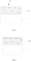
FIG. 2 to FIG. 7 are each a schematic structural diagram corresponding to a step in a thin-film deposition method according to an embodiment of the present application; and -
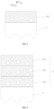
FIG. 8 to FIG. 11 are each a schematic structural diagram of a semiconductor device according to an embodiment of depositing a thin-film layer according to a thin-film deposition method according to the present application. - 1-substrate, 2-thin-film layer, 210-first deposited layer, 211-purified deposited layer, 212-filling layer, 220-second deposited layer, 3-gate.
- In order to make the objectives, technical solutions and advantages of the embodiments of the present application clearer, the following clearly and completely describes the technical solutions in the embodiments of the present application with reference to the accompanying drawings in the embodiments of the present application. Apparently, the described embodiments are some rather than all of the embodiments of the present application. All other embodiments obtained by a person skilled in the art based on the embodiments of the present application without creative efforts should fall within the protection scope of the present application. It should be noted that without conflict, the embodiments in the present application and features in the embodiments may be combined with each other.
- A thin-film deposition method and a semiconductor device provided in the present application are described in detail below with reference to the accompanying drawings and specific implementations.
- As shown in
FIG. 1 to FIG. 7 , the thin-film deposition method in this embodiment of the present application includes: Step S1: Provide asubstrate 1. Step S2: Perform thin-film deposition on thesubstrate 1 by using a thin-film deposition technology, and forming a first depositedlayer 210 when the thin-film deposition reaches a first predetermined condition. Step S3: Introduce a purge gas to perform impurity purge treatment on the first depositedlayer 210, to form a purified depositedlayer 211. Step S4: Repeatedly perform step S2 and step S3 for N times, to formN+ 1 purified depositedlayers 211, where N is an integer greater than or equal to 0. Step S5: Form a thin-film layer 2 by the N+1 purified depositedlayers 211. - As shown in
FIG. 2 , step S2 in the thin-film deposition method in this embodiment of the present application is performing thin-film deposition on thesubstrate 1 by using the thin-film deposition technology, and forming the first depositedlayer 210 when the thin-film deposition reaches the first predetermined condition. The thin-film deposition technology used is PECVD or PEALD. - In some embodiments, the thin-film deposition technology used is PECVD or PEALD.
- In some embodiments, the first predetermined condition is that a thickness of thin-film deposition is 1/20 to 1/2 of a total thickness of a thin-film layer. In other embodiments, the first predetermined condition is that a number of thin-film deposition cycles is 1/20 to 1/2 of a total number of deposition cycles. Specifically, the first predetermined condition may be that the thickness of thin-film deposition is 1/20, 1/15, 1/10, 1/5, 1/4, 1/3 or 1/2 of the total thickness of the thin-film layer, or the first predetermined condition may be that the number of thin-film deposition cycles is 1/20, 1/15, 1/10, 1/5, 1/4, 1/3 or 1/2 of the total number of deposition cycles.
- In some embodiments, the first predetermined condition is that the thickness of thin-film deposition is 1 nm to 20 nm. In other embodiments, the first predetermined condition is that the number of thin-film deposition cycles is 1 to 20.
- As shown in
FIG. 2 to FIG. 4 , step S3 in the thin-film deposition method in this embodiment of the present application includes: introducing the purge gas, where a first gas is produced by a chemical reaction between the purge gas and the impurity in the first depositedlayer 210, and the first gas is discharged from the first depositedlayer 210, to purge the impurity in the first depositedlayer 210 and form the purified depositedlayer 211. - In this embodiment of the present application, the substrate includes a substrate and a gate structure formed thereon, the thin-film layer includes a silicon nitride thin-film layer, the impurity includes one or more of a chlorine element, an oxygen element or a hydrogen element, and the purge gas includes hydrogen or ammonia. Specifically, step S3 in the thin-film deposition method includes: introducing a purge gas H2 into the first deposited
layer 210, where a first gas is produced by a chemical reaction between H2 and the chlorine element or the oxygen element in the first deposited layer 210: the hydrogen chloride and the water vapor, and the hydrogen chloride and the water vapor are discharged from the first depositedlayer 210, to purge the chlorine element and the oxygen element in the first depositedlayer 210 and form the purified depositedlayer 211. - When a traditional thin-film deposition technology is used to form the deposited layer, the deposited layer contains the impurity, which will reduce the stability of the deposited layer, thus reducing the protective effect of the thin-film layer on the substrate and affecting the service life of the substrate. According to the present application, the impurity content of the formed thin-film layer is greatly reduced by performing the impurity purge treatment on the deposited layer, such that the protective effect of the thin-film layer on the substrate is improved and the service life of the substrate is prolonged.
- As shown in
FIG. 5 , step S4 in the thin-film deposition method in this embodiment of the present application is repeatedly performing step S2 and step S3 for N times to form the N+1 purified depositedlayers 211, where N is an integer greater than or equal to 0. - In some embodiments, in step S4 in the thin-film deposition method, step S2 and step S3 may not be repeated, and one purified deposited
layer 211 is formed; or step S2 and step S3 may be repeated for one or more times, to form two or more purified depositedlayers 211. A number of repetition times of step S2 and step S3 is determined based on requirements on the thin-film layer in actual production. If the required thin-film layer is relatively thick or the required total number of deposition cycles is relatively large, the number of repetition times of step S2 and step S3 may be larger. If the required thin-film layer is thin or the required total number of deposition cycles is relatively small, the number of repetition times of step S2 and step S3 may be one or two, or step S2 and step S3 may not be repeated. For example, step S4 in the thin-film deposition method is repeatedly performing step S2 and step S3 twice to form three purified depositedlayers 211. - When two or more purified deposited
layers 211 are formed, the first predetermined condition for forming each purified depositedlayer 211 is independent, and each first predetermined condition is independently that the thickness of thin-film deposition is 1/20 to 1/2 of the total thickness of the thin-film layer or the number of thin-film deposition cycles is 1/20 to 1/2 of the total number of deposition cycles. - The stability of the thin-film layer can be improved by performing the impurity purge treatment on the first deposited layer. When thin-film deposition and impurity purge treatment are repeatedly performed, not only can a thick thin-film layer be formed, but also impurity purge treatment can be performed on each thin-film layer, such that impurities inside the thick thin-film layer can also be purged. This avoids that only impurities on the surface of the thin-film layer or a thinner thin-film are purged, but impurities inside the thick thin-film layer cannot be purged.
- As shown in
FIG. 6 , after step S4 and before step S5, the thin-film deposition method in this embodiment of the present application further includes: adding a filling material into a formed third purified depositedlayer 211 for filling gaps left by purging the impurity in the purified depositedlayer 211, to form afilling layer 212, where the formed thin-film layer 2 includes at least onefilling layer 212. The filling material includes a nitrogen-containing substance. - In some embodiments, the filling material may be added into any formed purified deposited
layer 211 for filling treatment, or the filling material may be added to all the formed purified depositedlayers 211 for filling treatment. - In some embodiments, in the thin-film layer formation process, the first formed layer is the
filling layer 212, and the last formed layer is thefilling layer 212. The formed thin-film layer may include only two fillinglayers 211. Or the formed thin-film layer may include one or more of the purified depositedlayer 211, the second depositedlayer 220 and thefilling layer 211, between the two filling layers. The presence forms of the purified depositedlayer 211, the second depositedlayer 220 and thefilling layer 211 may be arbitrary, the number of layers may be arbitrary, and the stacking sequence may be arbitrary. - Since the impurity in the first deposited layer is purged by the purge gas, gaps are left in the formed purified deposited layer, and filling the gaps with the filling material to form the filling layer improves the stability of the thin-film layer. When the first layer in the thin-film layer is the filling layer, the stable filling layer can protect the substrate well, for example, the substrate or the gate. When the last layer in the thin-film layer is the filling layer, the impact of external air on the performance of the thin-film layer can be avoided, and the stability of the thin-film layer can be further improved. Therefore, when the first layer and the last layer in the thin-film layer are the filling layer, the thin-film layer can have high stability, such that the thin-film layer can protect the substrate well.
- As shown in
FIG. 7 , step S5 in the thin-film deposition method in this embodiment of the present application includes: performing thin-film deposition on thefilling layer 212 by using the thin-film deposition technology, forming a second depositedlayer 220 when the thin-film deposition reaches a second predetermined condition, no-performing the impurity purge treatment on the second depositedlayer 220, and forming the thin-film layer 2 by the purified depositedlayer 211, thefilling layer 212 and the second depositedlayer 220. The thin-film layer 2 is a silicon nitride thin-film layer. - In other embodiments, after step S1 and before step S2, the thin-film deposition method may further include: performing the thin-film deposition on the
substrate 1 by using the thin-film deposition technology, forming a second depositedlayer 220 when the thin-film deposition reaches a second predetermined condition, and no-performing the impurity purge treatment on the second depositedlayer 220. - In other embodiments, after step S1 and before step S2, the thin-film deposition method may further include: performing thin-film deposition on the
substrate 1 by using the thin-film deposition technology, forming a first depositedlayer 210 when the thin-film deposition reaches the first predetermined condition, introducing a purge gas to purge an impurity in the formed first depositedlayer 210, to form a purified depositedlayer 211, and adding a filling material to the formed purified depositedlayer 211 for filling treatment, to form afilling layer 212. - In other embodiments, when a plurality of purified deposited
layers 211 are formed, between forming any two adjacent purified depositedlayers 211, the thin-film deposition method includes: performing the thin-film deposition on a lower purified depositedlayer 211 by using the thin-film deposition technology, forming a second depositedlayer 220 when the thin-film deposition reaches the second predetermined condition, no-performing the impurity purge on the second depositedlayer 220, and then performing thin-film deposition on the second depositedlayer 220 to form an upper purified depositedlayer 211. That is, the thin-film layer 2 includes the purified depositedlayer 211, the second depositedlayer 220, and the purified depositedlayer 211 that are sequentially stacked. - Before the first purified deposited layer is formed, or after the last purified deposited layer is formed, or between any two adjacent purified deposited layers are formed, thin-film deposition is performed by using the thin-film deposition technology to form the second deposited layer, and impurity purge treatment on the second deposited layer is not performed. The purified deposited layer and the second deposited layer without impurity purge treatment form the thin-film layer together. This can not only improve the stability of the thin-film layer, but also reduce the cost while forming a relatively thick thin-film layer.
- In some embodiments, the second predetermined condition is that a thickness of thin-film deposition is 1/20 to 1/2 of a total thickness of the thin-film layer. In other embodiments, the second predetermined condition is that a number of thin-film deposition cycles is 1/20 to 1/2 of a total number of deposition cycles.
- As shown in
FIG. 8 , a thin-film deposition method in another embodiment of the present application includes: Step S1': Provide asubstrate 1. Step S2': Perform thin-film deposition on thesubstrate 1 by using a thin-film deposition technology, and forming a first depositedlayer 210 when the thin-film deposition reaches a first predetermined condition. Step S3': Introduce a purge gas to perform impurity purge treatment on the first depositedlayer 210, to form a purified depositedlayer 211; and add a filling material into the purified depositedlayer 211 for filling treatment, to form afilling layer 212. Step S4': Repeatedly performing step S2' and the impurity purge operation in step S3' for N1 times, to form N1 purified deposited layers 211. Step S5': Perform thin-film deposition on the N1 purified depositedlayers 211 to form fillinglayers 212, where N1 is an integer greater than or equal to 0. For forming thefilling layer 212 in step S5', refer to steps S2' and S3'. - A thin-film deposition method in another embodiment of the present application includes: Step S1": Provide a
substrate 1. Step S2": Perform thin-film deposition on thesubstrate 1 by using a thin-film deposition technology, and form a first depositedlayer 210 when the thin-film deposition reaches a first predetermined condition. Step S3": Introduce a purge gas to perform impurity purge treatment on the first depositedlayer 210, to form a purified depositedlayer 211; and add a filling material into the formed purified depositedlayer 211 for filling treatment, to form afilling layer 212. Step S4": Repeatedly perform step S2" and the impurity purge operation in step S3" for N2 times, to form N2 purified deposited layers 211. Step S5": Perform thin-film deposition by using the thin-film deposition technology, form a second depositedlayer 220 when the thin-film deposition reaches a second predetermined condition; perform thin-film deposition on the second depositedlayer 220 to form N3 purified depositedlayers 211, and perform thin-film deposition on the N3 purified depositedlayers 211 to form afilling layer 212, where N2 and N3 are each an integer greater than or equal to 0. For forming the N3 purified depositedlayers 211 and thefilling layer 212 in step S5", refer to steps S2" and S3". - As shown in
FIG. 8 , a semiconductor device according to an embodiment of the present application includes agate 3 and a thin-film layer 2 disposed on a surface of thegate 3, where the thin-film layer 2 is formed according to the thin-film deposition method in the present application. The thin-film layer 2 includes afirst filling layer 212, a first purified depositedlayer 211, a second purified depositedlayer 211, and asecond filling layer 212 that are stacked on the surface of thegate 3 from inside to outside. Impurity purge treatment is performed on the purified depositedlayer 211, and thefilling layer 212 is formed by filling a nitrogen-containing substance into the purified depositedlayer 211. - As shown in
FIG. 9 , a semiconductor device according to another embodiment of the present application includes agate 3 and a thin-film layer 2 disposed on a surface of thegate 3. The thin-film layer 2 includes a first purified depositedlayer 211, a second purified depositedlayer 211, afilling layer 212, and a second depositedlayer 220 that are stacked on the surface of thegate 3 from inside to outside. Impurity purge treatment is not performed on the second depositedlayer 220. - As shown in
FIG. 10 , a semiconductor device according to another embodiment of the present application includes agate 3 and a thin-film layer 2 disposed on a surface of thegate 3. The thin-film layer 2 includes a purified depositedlayer 211, afilling layer 212, and a purified depositedlayer 211 that are stacked on the surface of thegate 3 from inside to outside. - As shown in
FIG. 11 , a semiconductor device according to another embodiment of the present application includes agate 3 and a thin-film layer 2 disposed on a surface of thegate 3. The thin-film layer 2 includes a purified depositedlayer 211, a second depositedlayer 220, and a purified depositedlayer 211 that are stacked on the surface of thegate 3 from inside to outside. - In some embodiments, a thickness of the thin-
film layer 2 is 1 nm to 50 nm, and a ratio of a total thickness of the purified depositedlayer 211 to a total thickness of the second depositedlayer 220 is 1: 1 to 10: 1. When the thin-film layer 2 includes thefilling layer 212, the total thickness of the purified depositedlayer 211 may include a thickness of thefilling layer 212. Specifically, the thickness of the thin-film layer 2 may be 1 nm, 5 nm, 10 nm, 20 nm, 25 nm, 30 nm, 40 nm or 50 nm, and a ratio of a total thickness of the purified depositedlayer 211 and thefilling layer 212 to a total thickness of the second depositedlayer 220 is 1: 1, 2: 1, 3: 1, 5: 1, 6: 1, 8: 1 or 10: 1. - It should be noted that relational terms herein such as upper, lower, inside, outside, front, behind, in the middle of, first and second are only used to distinguish one entity or operation from another entity or operation without necessarily requiring or implying any actual such relationship or order between such entities or operations. It should be noted that terms "including", "comprising", or any other variants thereof are intended to cover non-exclusive inclusion, such that a process, method, article, or device including a series of elements includes not only those elements but also other elements not explicitly listed, or elements inherent to such a process, method, article, or device. Without more restrictions, the elements defined by the sentence "including a ..." do not exclude the existence of other identical elements in a process, method, article, or device including the elements.
- At last, it should be noted that the above embodiments are only used for describing the technical solutions of the present application, and are not intended to limit the present application. Although the present application is described in detail with reference to the foregoing examples, those of ordinary skill in the art should understand that they can still modify the technical solutions described in the foregoing examples, or make substitutions on some technical features therein. These modifications or substitutions do not make the essence of the corresponding technical solutions deviate from the scope of the technical solutions of the examples of the present disclosure.
- It should be noted that, the present application is not limited to the precise structures that have been described above and shown in the accompanying drawings, and can be modified and changed in many ways without departing from the scope of the present disclosure. The scope of the present application is defined by the appended claims.
- In the thin-film deposition method provided in the present application, the thin-film deposition technology is adopted to form the deposited layer, and impurity purge treatment is performed on the deposited layer, such that the impurity content of the formed thin-film layer is greatly reduced. The semiconductor device provided in the present application is prepared by covering the thin-film layer according to the present application on the surface of the gate. Because the impurity content of the thin-film layer is low, the gate can be better protected and the service life of the semiconductor device is remarkably prolonged.
Claims (19)
- A thin-film deposition method, comprising:step S1: providing a substrate;step S2: performing thin-film deposition on the substrate by using a thin-film deposition technology, and forming a first deposited layer when the thin-film deposition reaches a first predetermined condition;step S3: introducing a purge gas to perform impurity purge treatment on the first deposited layer, to form a purified deposited layer;step S4: repeatedly performing step S2 to step S3 for N times, to form N+1 purified deposited layers, wherein N is an integer greater than or equal to 0; andstep S5: forming a thin-film layer by the N+1 purified deposited layers.
- The thin-film deposition method according to claim 1, further comprising: adding a filling material to at least one formed purified deposited layer for filling gaps left by purging the impurity in the purified deposited layer, to form a filling layer, wherein the formed thin-film layer comprises at least one filling layer.
- The thin-film deposition method according to claim 2, wherein the filling material comprises a nitrogen-containing substance.
- The thin-film deposition method according to claim 1, wherein after step S1 and before step S2, or after step S4 and before step S5, the thin-film deposition method further comprises: performing the thin-film deposition by using the thin-film deposition technology, forming a second deposited layer when the thin-film deposition reaches a second predetermined condition, and no-performing the impurity purge treatment on the second deposited layer.
- The thin-film deposition method according to claim 1, wherein when N is a positive integer greater than or equal to 1, a plurality of purified deposited layers are formed; and between forming any two adjacent purified deposited layers, the thin-film deposition method further comprises: performing the thin-film deposition by using the thin-film deposition technology, forming a second deposited layer when the thin-film deposition reaches a second predetermined condition, and no-performing the impurity purge treatment on the second deposited layer.
- The thin-film deposition method according to claim 1, wherein the thin-film deposition technology in step S2 is plasma enhanced chemical vapor deposition or plasma enhanced atomic layer deposition.
- The thin-film deposition method according to claim 1, wherein the first predetermined condition in step S2 is that a thickness of thin-film deposition is 1/20 to 1/2 of a total thickness of the thin-film layer, or a number of thin-film deposition cycles is 1/20 to 1/2 of a total number of deposition cycles.
- The thin-film deposition method according to claim 1, wherein when the N+1 purified deposited layers are formed, the first predetermined condition for forming each purified deposited layer is independent, and each first predetermined condition is independently that a thickness of thin-film deposition is 1/20 to 1/2 of a total thickness of the thin-film layer, or a number of thin-film deposition cycles is 1/20 to 1/2 of a total number of deposition cycles.
- The thin-film deposition method according to claim 4 or 5, wherein the second predetermined condition is that a thickness of thin-film deposition is 1/20 to 1/2 of a total thickness of the thin-film layer, or a number of thin-film deposition cycles is 1/20 to 1/2 of a total number of deposition cycles.
- The thin-film deposition method according to claim 1, wherein the purge gas in step S3 comprises hydrogen or ammonia.
- The thin-film deposition method according to claim 1, wherein the thin-film layer comprises a silicon nitride thin-film layer, and the impurity comprises one or more of a chlorine element, an oxygen element or a hydrogen element.
- The thin-film deposition method according to claim 1, wherein step S3 comprises: when the thin-film deposition reaches the first predetermined condition, forming the first deposited layer, and introducing the purge gas into the first deposited layer, wherein a first gas is produced by a chemical reaction between the purge gas and the impurity in the first deposited layer, and the first gas is discharged from the first deposited layer, to purge the impurity in the first deposited layer.
- The thin-film deposition method according to claim 12, wherein the first gas is one or two of water vapor or hydrogen chloride.
- A semiconductor device, comprising a gate and a thin-film layer disposed on a surface of the gate, wherein the thin-film layer is formed by using the thin-film deposition method according to claim 1.
- The semiconductor device according to claim 14, wherein the thin-film layer comprises a filling layer formed by filling a purified deposited layer with a nitrogen-containing substance.
- The semiconductor device according to claim 14, wherein the thin-film layer further comprises a second deposited layer, and the second deposited layer is not performed the impurity purge treatment.
- The semiconductor device according to claim 16, wherein the thin-film layer comprises the second deposited layer and the purified deposited layer, the second deposited layer and the purified deposited layer are stacked on the surface of the gate from inside to outside; or the thin-film layer comprises the purified deposited layer and the second deposited layer, the purified deposited layer and the second deposited layer are stacked on the surface of the gate from inside to outside; or the thin-film layer comprises the purified deposited layer, the second deposited layer, and the purified deposited layer, the purified deposited layer, the second deposited layer, and the purified deposited layer are stacked on the surface of the gate from inside to outside.
- The semiconductor device according to claim 14, wherein a thickness of the thin-film layer is 1 nm to 50 nm, the first predetermined condition is that a thickness of thin-film deposition is 1 nm to 20 nm or a number of thin-film deposition cycles is 1 to 20.
- The semiconductor device according to claim 16, wherein a ratio of a total thickness of the purified deposited layer to a total thickness of the second deposited layer is 1: 1 to 10: 1.
Applications Claiming Priority (2)
| Application Number | Priority Date | Filing Date | Title |
|---|---|---|---|
| CN202110753708.4A CN115565861A (en) | 2021-07-02 | 2021-07-02 | Thin film deposition method and semiconductor device |
| PCT/CN2021/118694 WO2023272951A1 (en) | 2021-07-02 | 2021-09-16 | Thin film deposition method and semiconductor device |
Publications (2)
| Publication Number | Publication Date |
|---|---|
| EP4135011A1 true EP4135011A1 (en) | 2023-02-15 |
| EP4135011A4 EP4135011A4 (en) | 2023-10-25 |
Family
ID=84044284
Family Applications (1)
| Application Number | Title | Priority Date | Filing Date |
|---|---|---|---|
| EP21928347.0A Pending EP4135011A4 (en) | 2021-07-02 | 2021-09-16 | Thin film deposition method and semiconductor device |
Country Status (4)
| Country | Link |
|---|---|
| US (1) | US20230005741A1 (en) |
| EP (1) | EP4135011A4 (en) |
| CN (1) | CN115565861A (en) |
| WO (1) | WO2023272951A1 (en) |
Family Cites Families (9)
| Publication number | Priority date | Publication date | Assignee | Title |
|---|---|---|---|---|
| JP2005310927A (en) * | 2004-04-20 | 2005-11-04 | Toshiba Corp | Deposition method of high quality silicon nitride film by ultraviolet irradiation |
| JP6088178B2 (en) * | 2011-10-07 | 2017-03-01 | 株式会社日立国際電気 | Semiconductor device manufacturing method, substrate processing apparatus, and program |
| JP6254848B2 (en) * | 2014-01-10 | 2017-12-27 | 株式会社日立国際電気 | Semiconductor device manufacturing method, substrate processing apparatus, and program |
| SG11201703195QA (en) * | 2014-10-24 | 2017-05-30 | Versum Materials Us Llc | Compositions and methods using same for deposition of silicon-containing film |
| JP6086934B2 (en) * | 2015-01-14 | 2017-03-01 | 株式会社日立国際電気 | Semiconductor device manufacturing method, substrate processing apparatus, and program |
| KR102125074B1 (en) * | 2015-08-31 | 2020-06-19 | 주식회사 원익아이피에스 | Method of fabricating nitride film |
| US10692773B2 (en) * | 2018-06-29 | 2020-06-23 | Taiwan Semiconductor Manufacturing Company, Ltd. | Forming nitrogen-containing low-K gate spacer |
| JP6960953B2 (en) * | 2019-03-20 | 2021-11-05 | 株式会社Kokusai Electric | Semiconductor device manufacturing methods, substrate processing methods, substrate processing equipment, and programs |
| WO2021059486A1 (en) * | 2019-09-27 | 2021-04-01 | 株式会社Kokusai Electric | Substrate treatment device, method for manufacturing semiconductor device, and program |
-
2021
- 2021-07-02 CN CN202110753708.4A patent/CN115565861A/en active Pending
- 2021-09-16 EP EP21928347.0A patent/EP4135011A4/en active Pending
- 2021-09-16 WO PCT/CN2021/118694 patent/WO2023272951A1/en not_active Ceased
-
2022
- 2022-01-20 US US17/648,448 patent/US20230005741A1/en active Pending
Also Published As
| Publication number | Publication date |
|---|---|
| WO2023272951A1 (en) | 2023-01-05 |
| CN115565861A (en) | 2023-01-03 |
| US20230005741A1 (en) | 2023-01-05 |
| EP4135011A4 (en) | 2023-10-25 |
Similar Documents
| Publication | Publication Date | Title |
|---|---|---|
| US9891521B2 (en) | Method for depositing thin film | |
| CN102082087B (en) | Comprise semiconductor device and the manufacture method thereof of carbon-containing electrode | |
| US20130119514A1 (en) | Method for manufacturing semiconductor device | |
| US8581319B2 (en) | Semiconductor stacks including catalytic layers | |
| US8890275B2 (en) | Optoelectronic device and method of fabricating the same | |
| KR20180010323A (en) | Deposition methods for uniform and conformal hybrid titanium oxide films | |
| JP2011034995A (en) | Method of manufacturing semiconductor device, and semiconductor device | |
| KR101176900B1 (en) | Method for manufacturing of semiconductor device | |
| US12040228B2 (en) | Semiconductor device and manufacturing method thereof | |
| KR100717770B1 (en) | Flash memory device having a dielectric film having a laminated structure including a zirconium oxide film and a manufacturing method thereof | |
| JP2023538465A (en) | Sealing structure, display panel, and display panel manufacturing method | |
| US20230005741A1 (en) | Thin-film deposition method and semiconductor device | |
| US20250220963A1 (en) | Hafnium nitride adhesion layer | |
| US12559838B2 (en) | Sealing structure and manufacturing method therefor | |
| JP2020031151A (en) | Semiconductor memory device and method of manufacturing the same | |
| US20210005463A1 (en) | Manufacturing method of semiconductor device and etching gas | |
| CN216958044U (en) | Oxide semiconductor thin film transistor with improved insulating layer | |
| KR100857872B1 (en) | Semiconductor element and method for manufacturing same for preventing lifting | |
| CN215008274U (en) | Film packaging structure suitable for folding flexible display | |
| US10804494B2 (en) | Display device, display panel and manufacturing method thereof | |
| US20250210358A1 (en) | Capacitor electrode forming method | |
| TWI906158B (en) | Method of forming capacitor structure | |
| US20250379054A1 (en) | Method of forming hard mask structure | |
| US20060024441A1 (en) | Method of forming metal oxide and semimetal oxide | |
| KR20040053459A (en) | Method For Forming Barrier Metal in the semiconductor device |
Legal Events
| Date | Code | Title | Description |
|---|---|---|---|
| STAA | Information on the status of an ep patent application or granted ep patent |
Free format text: STATUS: UNKNOWN |
|
| STAA | Information on the status of an ep patent application or granted ep patent |
Free format text: STATUS: THE INTERNATIONAL PUBLICATION HAS BEEN MADE |
|
| PUAI | Public reference made under article 153(3) epc to a published international application that has entered the european phase |
Free format text: ORIGINAL CODE: 0009012 |
|
| STAA | Information on the status of an ep patent application or granted ep patent |
Free format text: STATUS: REQUEST FOR EXAMINATION WAS MADE |
|
| 17P | Request for examination filed |
Effective date: 20220906 |
|
| AK | Designated contracting states |
Kind code of ref document: A1 Designated state(s): AL AT BE BG CH CY CZ DE DK EE ES FI FR GB GR HR HU IE IS IT LI LT LU LV MC MK MT NL NO PL PT RO RS SE SI SK SM TR |
|
| A4 | Supplementary search report drawn up and despatched |
Effective date: 20230921 |
|
| RIC1 | Information provided on ipc code assigned before grant |
Ipc: H01L 21/02 20060101ALI20230915BHEP Ipc: C23C 16/44 20060101ALI20230915BHEP Ipc: C23C 16/455 20060101ALI20230915BHEP Ipc: C23C 16/50 20060101ALI20230915BHEP Ipc: H01L 29/51 20060101ALI20230915BHEP Ipc: H01L 21/28 20060101AFI20230915BHEP |
|
| DAV | Request for validation of the european patent (deleted) | ||
| DAX | Request for extension of the european patent (deleted) |