EP4134688A2 - Electronic circuit testing methods and systems - Google Patents
Electronic circuit testing methods and systems Download PDFInfo
- Publication number
- EP4134688A2 EP4134688A2 EP22186502.5A EP22186502A EP4134688A2 EP 4134688 A2 EP4134688 A2 EP 4134688A2 EP 22186502 A EP22186502 A EP 22186502A EP 4134688 A2 EP4134688 A2 EP 4134688A2
- Authority
- EP
- European Patent Office
- Prior art keywords
- node
- transistor
- current
- low
- coupled
- Prior art date
- Legal status (The legal status is an assumption and is not a legal conclusion. Google has not performed a legal analysis and makes no representation as to the accuracy of the status listed.)
- Withdrawn
Links
Images



Classifications
-
- H—ELECTRICITY
- H03—ELECTRONIC CIRCUITRY
- H03K—PULSE TECHNIQUE
- H03K17/00—Electronic switching or gating, i.e. not by contact-making and –breaking
- H03K17/16—Modifications for eliminating interference voltages or currents
- H03K17/161—Modifications for eliminating interference voltages or currents in field-effect transistor switches
- H03K17/162—Modifications for eliminating interference voltages or currents in field-effect transistor switches without feedback from the output circuit to the control circuit
-
- H—ELECTRICITY
- H02—GENERATION; CONVERSION OR DISTRIBUTION OF ELECTRIC POWER
- H02M—APPARATUS FOR CONVERSION BETWEEN AC AND AC, BETWEEN AC AND DC, OR BETWEEN DC AND DC, AND FOR USE WITH MAINS OR SIMILAR POWER SUPPLY SYSTEMS; CONVERSION OF DC OR AC INPUT POWER INTO SURGE OUTPUT POWER; CONTROL OR REGULATION THEREOF
- H02M1/00—Details of apparatus for conversion
- H02M1/32—Means for protecting converters other than automatic disconnection
- H02M1/34—Snubber circuits
- H02M1/344—Active dissipative snubbers
-
- G—PHYSICS
- G01—MEASURING; TESTING
- G01R—MEASURING ELECTRIC VARIABLES; MEASURING MAGNETIC VARIABLES
- G01R31/00—Arrangements for testing electric properties; Arrangements for locating electric faults; Arrangements for electrical testing characterised by what is being tested not provided for elsewhere
- G01R31/40—Testing power supplies
- G01R31/42—AC power supplies
-
- H—ELECTRICITY
- H02—GENERATION; CONVERSION OR DISTRIBUTION OF ELECTRIC POWER
- H02M—APPARATUS FOR CONVERSION BETWEEN AC AND AC, BETWEEN AC AND DC, OR BETWEEN DC AND DC, AND FOR USE WITH MAINS OR SIMILAR POWER SUPPLY SYSTEMS; CONVERSION OF DC OR AC INPUT POWER INTO SURGE OUTPUT POWER; CONTROL OR REGULATION THEREOF
- H02M3/00—Conversion of DC power input into DC power output
- H02M3/02—Conversion of DC power input into DC power output without intermediate conversion into AC
- H02M3/04—Conversion of DC power input into DC power output without intermediate conversion into AC by static converters
- H02M3/10—Conversion of DC power input into DC power output without intermediate conversion into AC by static converters using discharge tubes with control electrode or semiconductor devices with control electrode
- H02M3/145—Conversion of DC power input into DC power output without intermediate conversion into AC by static converters using discharge tubes with control electrode or semiconductor devices with control electrode using devices of a triode or transistor type requiring continuous application of a control signal
- H02M3/155—Conversion of DC power input into DC power output without intermediate conversion into AC by static converters using discharge tubes with control electrode or semiconductor devices with control electrode using devices of a triode or transistor type requiring continuous application of a control signal using semiconductor devices only
- H02M3/156—Conversion of DC power input into DC power output without intermediate conversion into AC by static converters using discharge tubes with control electrode or semiconductor devices with control electrode using devices of a triode or transistor type requiring continuous application of a control signal using semiconductor devices only with automatic control of output voltage or current, e.g. switching regulators
- H02M3/158—Conversion of DC power input into DC power output without intermediate conversion into AC by static converters using discharge tubes with control electrode or semiconductor devices with control electrode using devices of a triode or transistor type requiring continuous application of a control signal using semiconductor devices only with automatic control of output voltage or current, e.g. switching regulators including plural semiconductor devices as final control devices for a single load
-
- G—PHYSICS
- G01—MEASURING; TESTING
- G01R—MEASURING ELECTRIC VARIABLES; MEASURING MAGNETIC VARIABLES
- G01R31/00—Arrangements for testing electric properties; Arrangements for locating electric faults; Arrangements for electrical testing characterised by what is being tested not provided for elsewhere
- G01R31/327—Testing of circuit interrupters, switches or circuit-breakers
- G01R31/3277—Testing of circuit interrupters, switches or circuit-breakers of low voltage devices, e.g. domestic or industrial devices, such as motor protections, relays, rotation switches
-
- H—ELECTRICITY
- H03—ELECTRONIC CIRCUITRY
- H03K—PULSE TECHNIQUE
- H03K2217/00—Indexing scheme related to electronic switching or gating, i.e. not by contact-making or -breaking covered by H03K17/00
- H03K2217/0063—High side switches, i.e. the higher potential [DC] or life wire [AC] being directly connected to the switch and not via the load
-
- H—ELECTRICITY
- H03—ELECTRONIC CIRCUITRY
- H03K—PULSE TECHNIQUE
- H03K2217/00—Indexing scheme related to electronic switching or gating, i.e. not by contact-making or -breaking covered by H03K17/00
- H03K2217/0072—Low side switches, i.e. the lower potential [DC] or neutral wire [AC] being directly connected to the switch and not via the load
-
- H—ELECTRICITY
- H03—ELECTRONIC CIRCUITRY
- H03K—PULSE TECHNIQUE
- H03K2217/00—Indexing scheme related to electronic switching or gating, i.e. not by contact-making or -breaking covered by H03K17/00
- H03K2217/0081—Power supply means, e.g. to the switch driver
Definitions
- the description relates to methods and systems of testing switching circuits, such as fly-back circuits, for instance.
- One or more embodiments may be applied in integrated circuits (briefly, ICs) comprising power MOSFETs, such as an engine control unit (briefly, ECU) of an automotive engine management system (briefly, EMS), for instance.
- ICs integrated circuits
- MOSFETs such as an engine control unit (briefly, ECU) of an automotive engine management system (briefly, EMS), for instance.
- An ECU or engine control module is an electronic control unit configured to process signals from sensors and control a series of actuators equipped on an (e.g., internal combustion) engine based on signals received from sensors equipped on the engine.
- An ECU may comprise (e.g., flyback) half-bridge switching circuits comprising power transistors, e.g., in MOSFET technology.
- Half-bridge switching circuits are known in the art, which may be used for driving inductive loads.
- a half-bridge circuit comprises a high-side switch and a low-side switch coupled between a supply voltage node and a reference voltage node (e.g., a ground node), the two switches having an intermediate, switching node therebetween.
- the switches in the half-bridge circuit may comprise solid state switches such as MOS field-effect transistors.
- the switching circuit may be provided within an integrated circuit (IC).
- the (e.g., inductive) load usually external to the half-bridge circuit, may be connected between the supply voltage node and the intermediate node of the half-bridge circuit in a so-called “low-side driver” configuration, or between the intermediate node of the half-bridge circuit and the reference voltage node in a so-called “high-side driver” configuration.
- the high-side switch and the low-side switch may be driven by respective complementary control signals switching between a high value ("1", e.g., to close the switch) and a low value ("0", e.g., to open the switch).
- the half-bridge circuit can be configured to discharge an external (e.g., inductive) load when the output is switched-off.
- an external (e.g., inductive) load when the output is switched-off.
- the low-side and/or high-side transistors can have a relatively big die size.
- AMR absolute maximum rating
- a drain stress test may involve applying at hot temperature (e.g., about 150-175 degrees) a drain-source voltage at least equal to the AMR of the power MOS for a certain time and to measure leakage before and after the application of the stress.
- hot temperature e.g., about 150-175 degrees
- a drain-source voltage at least equal to the AMR of the power MOS for a certain time and to measure leakage before and after the application of the stress.
- a fly-back (or clamping) circuit can feature these kind of power MOS to drive inductive loads.
- the clamping circuit works like a voltage regulator configure to impose on the output pin a certain voltage designed to properly discharge the inductance, with the voltage being a function of number of Zener diodes, power-MOS characteristic and driver pull-down current.
- the imposed voltage is above battery voltage and below AMR of the power-MOS.
- An object of one or more embodiments is to contribute in overcoming the aforementioned drawbacks.
- One or more embodiments may relate to a corresponding method.
- One or more embodiments may relate to a corresponding system.
- An energy management system configured to be equipped on-board an automotive (e.g., electrically powered) vehicle may be exemplary of such a system.
- One or more embodiments envisage a relatively simple circuit, driven to switch-off a (e.g., daisy-chained or Darlington-like) transistor of the fly-back circuit via a test mode signal.
- a e.g., daisy-chained or Darlington-like
- One or more embodiments provide the possibility to perform drain stress at target voltage, countering the risk of activating the fly-back circuit, in compliance with quality checks and without introducing additional resources.
- One or more embodiments provide benefits on product quality and cost.
- safety-guards e.g., redundancy or relay resistance
- redundancy or relay resistance e.g., redundancy or relay resistance
- a same reference symbol may be used to designate both a node/line in a circuit and a signal which may occur at that node or line.
- Figure 1A represents a circuit block diagram exemplary of a low-side configuration of a driver circuit 10A configured for driving a load L, in particular an inductive load L.
- the load L may be further coupled to a battery BAT, for instance the battery of an (e.g., electrically powered) automotive vehicle.
- the circuit 100 comprises:
- Figure 1B represents a circuit block diagram exemplary of a high-side configuration of a driver circuit 10B configured for driving a load L, in particular an inductive load L.
- the circuit 100 comprises:
- the pair of daisy-chained high-side transistors S 0H , HS and low-side transistors S 0L , LS may comprise solid state switches, such as MOS field-effect transistors, for instance.
- the high-side switch HS and a low-side switch LS are coupled between a supply voltage node BAT and a reference voltage node GND (e.g., a ground node).
- the supply voltage node BAT may be configured to receive a (e.g., positive) supply voltage (e.g., from a battery) while the reference voltage node GND may be configured to receive a (e.g., negative or zero) reference voltage.
- the high-side (daisy-chained, Darlington-like arrangement of) pair of transistors S 0H , HS and the low-side (daisy-chained, Darlington-like arrangement of) pair of transistors S 0L , LS can be coupled via respective nodes OUT, OUT_S that form an intermediate node.
- the amplifier 100A, 100B may comprise an input node C configured to receive a digital control signal com which switches between a first value (e.g., "low” or “0") and a second value (e.g., "high” or “1”) to drive commutation of the transistors HS, LS.
- a first value e.g., "low” or "0”
- a second value e.g., "high” or “1”
- the (inverting) amplifier stage 100A may propagate an inverted replica of the signal com to the low-side transistor LS
- the (non-inverting) amplifier 100B may propagate a replica of the signal com to the high-side switch HS.
- the amplifiers 100A, 100B may also bring their output signals to voltage levels adapted for driving the transistors HS, LS.
- Figure 2 is exemplary of a method of operating the LS configuration represented in Figure 1 .
- the presence of the clamping circuitry in the LS configuration makes it possible to refer to it also as a “flyback” or “clamping” circuit. This is due to its operation in discharging the (external) inductive load L, when intermediate output node OUT is switched-off, by the output itself, that is to ground PGND.
- the control signal com received at the node C of the amplifier 100A has the first value (e.g., "low” or "0")
- the current path of the low-side transistor LS between node OUT and node PGND is made conductive and the switch LS is in a first (e.g., "active") state.
- a discharge current I L from the inductance flows into the current flow path OUT-PGND.
- this current flow I L leads to an increase of the voltage at the first node OUT of the low-side transistor LS.
- a bias current I CL_B flows into the clamping circuitry, in particular into the resistance R LS .
- this clamping current I CL_G balances the pull-down current provided by the driver 100A in order to turn-on again power-MOS S 0L with the gate-source bias voltage V GS suitable to carry load current I L provided by the discharge of the inductance L.
- the clamping circuitry D 0 , DZ 1 , DZ 2 , R LS , S 0L can be modeled as a voltage limiter or regulator that limits the voltage level at the first node OUT of the low-side transistor at a threshold value V CLAMP suitable to properly discharge the inductance.
- this threshold Vclamp may be set as a function of power-MOS characteristic and driver pull-down current and designed so that the voltage level at the first node OUT of the low-side transistor LS is higher than battery voltage and lower than power-MOS of AMR.
- Performing stress-tests on the low-side 10A and high-side 10B circuit configurations may involve:
- Figure 3 is exemplary of a conventional arrangement configured to deactivate the clamping circuity of the low-side circuit portion 10A while performing stress tests involving voltage levels V STRESS at the first node OUT exceeding the threshold voltage level V CLAMP .
- the disabling arrangement 30 comprises:
- the method of disabling the clamping circuitry D Z1 , DZ 2 , D 0 , S 0L , R LS while testing the low-side circuit LS comprises:
- the voltage at which the clamping circuitry operates is raised to an increased voltage level, e.g., given by the sum of the threshold voltage Vclamp and the shifted voltage Vshift, Vclamp+Vshift.
- Vstress e.g., Vclamp+Vshift>V STRESS >Vclamp
- One or more cases may envisage a plurality of low-side 10A or high-side 10B circuit portions, for instance as in an H-bridge arrangement known per se.
- the shifted voltage level Vshift can be applied to each control node of each of the LS switches, taking into account the relevant current flow ( ⁇ 1mA) for coupling the arrangement 30 to each control node.
- a solution as exemplified in Figure 3 involves additional circuit resources on the testing side in order to provide the proper voltage V STRESS to the test mode pin TM. As a drawback, this can be a limitation for parallelism during testing. Moreover, the arrangement 30 has a non-negligible area footprint in terms of die size, as it is designed to sustain high voltage and involves dedicated routing for each LS output.
- an improved disabling arrangement 40 comprises: a test switch TS (e.g., a n-MOS transistor) having a control node TM configured to be coupled to a test voltage level V TM and a current path therethrough between a first node and a second node PGND, the first node coupled, via a resistance R TS , to the control node of the transistor S 0L and the second node coupled to the second node PGND of the low-side transistor LS.
- a test switch TS e.g., a n-MOS transistor
- the test switch TS is configured to drive the first transistor S 0L in the high-side pair of transistors S 0L , HS of the fly-back circuit 10A to make non-conductive (that is, switched “off”) or conductive (that is, switched “on”) the second transistor Hs in the pair of high-side transistors S 0L , HS based on the test mode signal V TM received at the test-mode node TM having a first (e.g., "1") or a second (e.g., "0") value, respectively.
- an alternative disabling arrangement 50 in particular suitable for testing the high-side transistor HS, comprises:
- a circuit as exemplified herein comprises a high-side transistor pair S 0H , HS and a low-side transistor pair S 0L , LS having a common intermediate node OUT_S, OUT.
- the high-side transistor pair S 0H , HS comprises a first transistor HS having a control node and a current flowpath therethrough configured to provide a current flow line between a supply voltage node OUT_D and the intermediate node OUT_S (or OUT) as well as a second transistor S 0H having a current flowpath therethrough coupled to the control node of the first transistor HS.
- the low-side transistor pair S 0L , LS comprises a third transistor LS having a control node and a current flowpath therethrough configured to provide a current flow line between the intermediate node OUT, OUT_S and the reference voltage node GND as well as a fourth transistor S 0L having a current flowpath therethrough coupled to the control node of the third transistor LS.
- the high-side transistor pair S 0H , HS and the low-side transistor pair S 0L , LS are configured to supply an inductive load L coupled either between the supply voltage node OUT_D, BAT and the intermediate node or between the intermediate node and the reference voltage node.
- a circuit as exemplified herein further comprises a drive node C configured to receive a switching drive signal com, the drive node C coupled to the control node of the first transistor HS in the high-side transistor pair S 0H , HS and to the control node of the third transistor LS in the low-side transistor pair S 0L , LS wherein the switching drive signal is applied 100A, 100B with opposite polarities to the control node of the first transistor HS and to the control node of the third transistor S 0L , LS.
- a circuit as exemplified herein further comprises:
- a circuit as exemplified herein further comprises testing circuitry 40 (or 50) comprising a test-mode node TM configured to receive a test-mode signal V TM , the testing circuitry configured to be coupled to at least one of the second transistor S 0H in the high-side transistor pair S 0H , HS and of the fourth transistor S 0L in the low-side transistor pair S 0L , LS to apply thereto the test-mode signal V TM wherein the at least one of the high-side transistor pair S 0H , HS and the low-side transistor pair S 0L , LS is made selectively conductive or non-conductive based on the test-mode signal V TM .
- the testing circuitry 40 comprises a testing transistor TS having a control node coupled to the test-mode node TM and a current flowpath therethrough between a first testing transistor node and a second testing transistor node, the first testing transistor node coupled, via a testing resistance R TS , to the fourth transistor S 0L in the low-side pair of transistors S 0L , LS and a second testing transistor node coupled to the reference node.
- the testing transistor TS is configured to drive the fourth transistor LS in the low-side transistor pair S 0L , LS, making non-conductive said current flow line of the third transistor LS in the low-side transistor pair S 0L , LS in response to the test-mode signal V TM having a first value during a first time interval.
- the testing circuitry 50 comprises a further testing transistor M1 having a control node coupled to the test-mode node TM and a current flowpath therethrough between a first testing transistor node coupled to a first current mirror arrangement of transistors M2, M3 and a second testing transistor node coupled to a reference current generator Iref referred to ground GND.
- the first current mirror arrangement M2, M3 is configured to provide a mirrored current that is a scaled replica of the current flowing in the current flow path of the further testing transistor M1, the mirrored current being scaled by a first scale factor.
- a second current mirror arrangement of transistors M4, M5 is coupled to the first current mirror arrangement M2, M3 and to the second transistor S 0H in the high-side transistor pair S 0H , HS, the second current mirror arrangement M4, M5 configured to provide a further mirrored current that is a scaled replica of the current mirrored by the first current mirror M2, M3, the further mirrored current being scaled by a second scale factor.
- the further testing transistor M1 is configured to drive the second transistor S 0H in the high-side transistor pair S 0H , HS, making non-conductive said current flow path between the supply voltage node and the intermediate node in response to the test-mode signal having a first value during a first time interval.
- the second current mirror M3, M4 comprises a limiting resistance Rpd coupled intermediate the second current mirror arrangement M4, M5 and said intermediate node.
- a half-bridge or fullbridge load driver circuit HS, LS and a disabling arrangement 40, 50 as exemplified herein may be implemented in an application-specific integrated circuit (ASIC) 100 which may be comprised, by way of example, in an energy management system (EMS) unit of an automotive vehicle, for instance an electrically powered vehicle.
- ASIC application-specific integrated circuit
- EMS energy management system
- Figure 6 is exemplary of one or more embodiments of a system 60 such as an energy management system (briefly, EMS) comprising a driver circuit 100 and a processing unit 600 (e.g., a microcontroller unit of a vehicle).
- EMS energy management system
- the processing unit 600 is configured to provide the control signal com and the test-enable signal TM to the driver circuit 100.
- the high-side clamping circuitry and the low-side clamping circuitry each comprise a chain of Zener diodes DZ 1 , DZ 2 coupled either between the supply voltage node and the intermediate node or between the intermediate node and said reference voltage node.
- the high-side clamping circuitry and the low-side clamping circuitry each further comprise a resistance R LS , R HS couple in parallel with a last Zener diode DZ 2 in the chain of Zener diodes DZ 1 , DZ 2 .
- a method of operating the circuit exemplified herein comprises applying a test-mode signal V TM to the test-mode node TM, the test-mode signal having a first value during a first time interval, and applying a stress voltage level V STRESS to at least one of said second transistor S 0H in the high-side transistor pair S 0H , HS and fourth transistor S 0L in the low-side transistor pair S 0L , LS during the first time interval in which the test-mode signal has the first value, wherein the stress voltage level V STRESS is above either the low-side or the high-side clamping voltage.
- the method further comprises limiting Rsw, Rpd, M1, M3 an amount of current that flows into the low-side or the high-side clamping circuitry and the testing circuitry during the first time interval in which the test-mode signal has the first value.
- Figure 7 is exemplary of one or more embodiments of a (e.g., electrically powered) vehicle V comprising a (e.g., energy management) system 60 according to the present disclosure, for instance equipped with the driver circuit 100 configured to control an inductive actuator L.
- a (e.g., electrically powered) vehicle V comprising a (e.g., energy management) system 60 according to the present disclosure, for instance equipped with the driver circuit 100 configured to control an inductive actuator L.
- a device 60 as exemplified herein comprises a circuit 100 as per the present disclosure and an inductive load L coupled either between said supply voltage node and said intermediate node or between said intermediate node and said reference voltage node.
- the device 60 further comprises an electrical supply source BAT configured to provide a voltage supply level coupled to said supply voltage node of the circuit 100.
- the device 60 further comprises a stress voltage source configured to provide a stress voltage level V STRESS either above the high-side clamping voltage or the low-side clamping voltage to at least one said supply voltage node and said intermediate node.
- the device 60 further comprises signal generating circuitry 600 configured to provide the test-mode signal V TM to the test-mode node TM.
- the low-side transistor pair S 0L , LS and the high-side transistor pair S 0H , HS are coupled to the inductive load L at said intermediate node and form a flyback circuit arrangement.
- the device 60 may be equipped onboard an automotive vehicle V, preferably an electrically powered automotive vehicle.
- One or more embodiments may thus provide improved accuracy in determining failures of a driver circuit for an inductive load, which may be particularly advantageous to fulfill safety requirements in the automotive field.
- an energy management system, EMS, unit configured to manage energy of the vehicle V comprises the device 60 as per the present disclosure.
Landscapes
- Engineering & Computer Science (AREA)
- Power Engineering (AREA)
- Physics & Mathematics (AREA)
- General Physics & Mathematics (AREA)
- Electronic Switches (AREA)
- Tests Of Electronic Circuits (AREA)
- Testing Of Individual Semiconductor Devices (AREA)
Abstract
Description
- The description relates to methods and systems of testing switching circuits, such as fly-back circuits, for instance.
- One or more embodiments may be applied in integrated circuits (briefly, ICs) comprising power MOSFETs, such as an engine control unit (briefly, ECU) of an automotive engine management system (briefly, EMS), for instance.
- An ECU or engine control module (ECM) is an electronic control unit configured to process signals from sensors and control a series of actuators equipped on an (e.g., internal combustion) engine based on signals received from sensors equipped on the engine.
- An ECU may comprise (e.g., flyback) half-bridge switching circuits comprising power transistors, e.g., in MOSFET technology.
- Half-bridge switching circuits are known in the art, which may be used for driving inductive loads.
- As conventional in the art, a half-bridge circuit comprises a high-side switch and a low-side switch coupled between a supply voltage node and a reference voltage node (e.g., a ground node), the two switches having an intermediate, switching node therebetween. The switches in the half-bridge circuit may comprise solid state switches such as MOS field-effect transistors.
- According to known arrangements, the switching circuit may be provided within an integrated circuit (IC). The (e.g., inductive) load, usually external to the half-bridge circuit, may be connected between the supply voltage node and the intermediate node of the half-bridge circuit in a so-called "low-side driver" configuration, or between the intermediate node of the half-bridge circuit and the reference voltage node in a so-called "high-side driver" configuration.
- According to known driving schemes, the high-side switch and the low-side switch may be driven by respective complementary control signals switching between a high value ("1", e.g., to close the switch) and a low value ("0", e.g., to open the switch).
- The half-bridge circuit can be configured to discharge an external (e.g., inductive) load when the output is switched-off. In order to do so, the low-side and/or high-side transistors can have a relatively big die size.
- These transistors may be subject to reliability tests during which relatively high voltages may be applied. The test may involve voltage levels equal or higher absolute maximum rating (briefly, AMR) parameters, that is a maximum voltage that an electronic component can sustain without damage between its (e.g., drain-source) terminals.
- For instance, a drain stress test may involve applying at hot temperature (e.g., about 150-175 degrees) a drain-source voltage at least equal to the AMR of the power MOS for a certain time and to measure leakage before and after the application of the stress.
- A fly-back (or clamping) circuit can feature these kind of power MOS to drive inductive loads. The clamping circuit works like a voltage regulator configure to impose on the output pin a certain voltage designed to properly discharge the inductance, with the voltage being a function of number of Zener diodes, power-MOS characteristic and driver pull-down current. In order to facilitate proper discharge of energy stored in the inductance, in particular in short time, and proper reliability during life-time of the IC, the imposed voltage is above battery voltage and below AMR of the power-MOS.
- At the same time, this is in contrast with the constraint to perform drain stress at a voltage equal or above AMR. Specifically, if an input voltage equal to the power MOS AMR voltage is applied at an input node of the fly-back, its control circuit drives the power MOS to be closed; this leads to uncontrolled current flowing into the MOS channel, potentially causing destruction of the electronic component itself.
- Existing solutions to meet these conflicting demands involve using a dedicated circuit to disable the fly-back circuit itself in order to counter interference thereof during execution of drain stress tests.
- Existing solutions suffer one or more of the following drawbacks:
- involve additional resources on the test side in order to provide the proper voltage to the test mode pin,
- limitation of parallelism during test performance,
- increase of overall test time, possibly leading to increased manufacturing costs,
- relevant overhead of the die size allocated for the top-level routing,
- increased area footprint, possibly leading to increased costs of production,
- cold tests at wafer level (EWS) may hardly be compatible with quality tests to be performed at high temperature,
- introduction of an additional testing flow leading to increased product cost,
- waiver of high temperature for quality tests, impacting on performance levels of the application system.
- An object of one or more embodiments is to contribute in overcoming the aforementioned drawbacks.
- According to one or more embodiments, that object can be achieved by means of a circuit having the features set forth in the claims that follow.
- One or more embodiments may relate to a corresponding method.
- One or more embodiments may relate to a corresponding system.
- An energy management system (EMS) configured to be equipped on-board an automotive (e.g., electrically powered) vehicle may be exemplary of such a system.
- The claims are an integral part of the technical teaching provided herein with reference to the embodiments.
- One or more embodiments envisage a relatively simple circuit, driven to switch-off a (e.g., daisy-chained or Darlington-like) transistor of the fly-back circuit via a test mode signal.
- One or more embodiments provide the possibility to perform drain stress at target voltage, countering the risk of activating the fly-back circuit, in compliance with quality checks and without introducing additional resources.
- One or more embodiments provide benefits on product quality and cost.
- In one or more embodiments, safety-guards (e.g., redundancy or relay resistance) against malfunctioning can be put in place.
- One or more embodiments will now be described, by way of non-limiting example only, with reference to the annexed Figures, wherein:
-
Figures 1A and 1B are diagrams exemplary of low-side and high-side circuit portions, respectively, -
Figures 2 is a diagram exemplary of operating the circuit exemplified inFigure 1A , -
Figures 3 is a diagram exemplary of a conventional testing arrangement of the circuit inFigure 1A , -
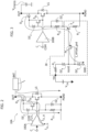
Figure 4 is a diagram exemplary of a circuit as per the present disclosure, -
Figure 5 is a diagram exemplary of an alternative embodiment of a circuit as per the present disclosure, -
Figure 6 is an exemplary diagram of system as per the present disclosure, -
Figure 7 is an exemplary diagram of a vehicle equipped with the system ofFigure 6 . - In the ensuing description, one or more specific details are illustrated, aimed at providing an in-depth understanding of examples of embodiments of this description. The embodiments may be obtained without one or more of the specific details, or with other methods, components, materials, etc. In other cases, known structures, materials, or operations are not illustrated or described in detail so that certain aspects of embodiments will not be obscured.
- Reference to "an embodiment" or "one embodiment" in the framework of the present description is intended to indicate that a particular configuration, structure, or characteristic described in relation to the embodiment is comprised in at least one embodiment. Hence, phrases such as "in an embodiment" or "in one embodiment" that may be present in one or more points of the present description do not necessarily refer to one and the same embodiment.
- Moreover, particular conformations, structures, or characteristics may be combined in any adequate way in one or more embodiments.
- The drawings are in simplified form and are not to precise scale.
- Throughout the figures annexed herein, like parts or elements are indicated with like references/numerals and a corresponding description will not be repeated for brevity.
- The references used herein are provided merely for convenience and hence do not define the extent of protection or the scope of the embodiments.
- For the sake of simplicity, in the following detailed description a same reference symbol may be used to designate both a node/line in a circuit and a signal which may occur at that node or line.
- By way of introduction to the detailed description of exemplary embodiments, reference may be first made to
Figures 1A and 1B . -
Figure 1A represents a circuit block diagram exemplary of a low-side configuration of adriver circuit 10A configured for driving a load L, in particular an inductive load L. The load L may be further coupled to a battery BAT, for instance the battery of an (e.g., electrically powered) automotive vehicle. - As exemplified in
Figure 1A , thecircuit 100 comprises: - a low-side transistor LS having a control node coupled to an
amplifier 100A configured to provide a control signal thereto and a current path therethrough between a first (e.g., drain) transistor node OUT and a second (e.g., source) transistor node PGND, the current path OUT-PGND configured to be made conductive or non-conductive in response to the signal provided by theamplifier 100A and received at the control node of the low-side transistor LS having a first value or a second value, respectively, - clamping circuitry comprising a further transistor S0L (e.g., forming a daisy-chained, Darlington-like arrangement together with the low-side transistor LS), a diode D0 (e.g., intermediate the daisy-chained, Darlington-like arrangement S0L, LS), Zener diodes DZ1, DZ2, and a resistance RLS, the clamping circuitry configured to facilitate discharge of a current flowing into the inductive load L, as discussed in the foregoing with reference to
Figure 2 . -
Figure 1B represents a circuit block diagram exemplary of a high-side configuration of adriver circuit 10B configured for driving a load L, in particular an inductive load L. - As exemplified in
Figure 1B , thecircuit 100 comprises: - a high-side transistor HS having a control node coupled to an
amplifier 100B configured to provide a control signal thereto and a current path therethrough between a first (e.g., drain) transistor node OUT_D coupled to the battery BAT and a second (e.g., source) transistor node OUT_S coupled to the inductive load L, the current path OUT_D-OUT_S configured to be made conductive or non-conductive in response to the control signal provided by thedriver 100A and received at the control node of the transistor HS having a first value or a second value, respectively, - clamping circuitry comprising a further transistor S0H (e.g., forming a daisy-chained, Darlington-like arrangement together with the high-side transistor HS), a diode D0 (e.g., intermediate the daisy-chained, Darlington-like arrangement S0H, HS), Zener diodes DZ1, DZ2, DZ3, and a resistance RLS, which is configured to operate in a manner substantially equal to that of
Figure 1A . - As exemplified in the Figures annexed herein, the pair of daisy-chained high-side transistors S0H, HS and low-side transistors S0L, LS may comprise solid state switches, such as MOS field-effect transistors, for instance.
- In a conventional half-bridge circuit arrangement, the high-side switch HS and a low-side switch LS are coupled between a supply voltage node BAT and a reference voltage node GND (e.g., a ground node). The supply voltage node BAT may be configured to receive a (e.g., positive) supply voltage (e.g., from a battery) while the reference voltage node GND may be configured to receive a (e.g., negative or zero) reference voltage.
- In one or more exemplary cases, the high-side (daisy-chained, Darlington-like arrangement of) pair of transistors S0H, HS and the low-side (daisy-chained, Darlington-like arrangement of) pair of transistors S0L, LS can be coupled via respective nodes OUT, OUT_S that form an intermediate node.
- In particular:
-
Figure 1A is exemplary of a low-side driver configuration 10A where the load L is connected between the supply voltage node BAT and the intermediate node OUT, and -
Figure 1B is exemplary of a high-side driver configuration 10B where the load L is connected between the intermediate node OUT S and ground GND. - As exemplified in
Figures 1A and 1B , theamplifier amplifier stage 100A may propagate an inverted replica of the signal com to the low-side transistor LS, and the (non-inverting)amplifier 100B may propagate a replica of the signal com to the high-side switch HS. Theamplifiers -
Figure 2 is exemplary of a method of operating the LS configuration represented inFigure 1 . - As exemplified in
Figure 2 , the presence of the clamping circuitry in the LS configuration makes it possible to refer to it also as a "flyback" or "clamping" circuit. This is due to its operation in discharging the (external) inductive load L, when intermediate output node OUT is switched-off, by the output itself, that is to ground PGND. - In particular, when the control signal com received at the node C of the
amplifier 100A has the first value (e.g., "low" or "0"), the current path of the low-side transistor LS between node OUT and node PGND is made conductive and the switch LS is in a first (e.g., "active") state. As a result, a discharge current IL from the inductance flows into the current flow path OUT-PGND. - As exemplified in
Figure 2 , this current flow IL leads to an increase of the voltage at the first node OUT of the low-side transistor LS. In the example considered, thanks to the presence of the clamping circuitry D0, DZ1, DZ2, RLS, S0L, if the voltage on the first node OUT of the low-side transistor LS exceeds a certain reference level (e.g., VCLAMP), a bias current ICL_B flows into the clamping circuitry, in particular into the resistance RLS. As a result of this bias current flow ICL_B in the resistance RLS, the voltage VRS = ICL_B*RLS across the resistance RLS increases up to a gate-biasing value for the gate of the power-MOS S0L, which is switched on as a result. In response to the switch-on of the switch S0L, a clamping current ICL_G flows into the current path through the nodes of the switch S0L. Finally, still in the considered example, the clamping current ICL_G is sourced to the control (e.g., gate) node of the switch S0L. In particular, this clamping current ICL_G balances the pull-down current provided by thedriver 100A in order to turn-on again power-MOS S0L with the gate-source bias voltage VGS suitable to carry load current IL provided by the discharge of the inductance L. - As exemplified in
Figure 2 , the clamping circuitry D0, DZ1, DZ2, RLS, S0L can be modeled as a voltage limiter or regulator that limits the voltage level at the first node OUT of the low-side transistor at a threshold value VCLAMP suitable to properly discharge the inductance. - For instance, this threshold Vclamp may be set as a function of power-MOS characteristic and driver pull-down current and designed so that the voltage level at the first node OUT of the low-side transistor LS is higher than battery voltage and lower than power-MOS of AMR. In particular, the threshold voltage value VCLAMP may be expressed as:

- N is a number of Zener diodes DZ1, DZ2,
- VDZ is the voltage limit of each Zener diode (e.g., VDZ = 5 V),
- VBE is the forward activation voltage of the diode D0, (e.g., VBE ~0.7 V);
- VGS_S0L is the bias voltage of the transistor S0L.
- Performing stress-tests on the low-
side 10A and high-side 10B circuit configurations, may involve: - for the low-
side circuit 10A, applying a certain stress-test voltage VSTRESS (e.g., VSTRESS>VCLAMP) to a node of the circuit 10a used for test mode purpose and to transfer this voltage shift to the clamping ground reference PGND, and/or - for the
high side circuit 10B, forcing a gate voltage level to keep the power MOS in an OFF state. -
Figure 3 is exemplary of a conventional arrangement configured to deactivate the clamping circuity of the low-side circuit portion 10A while performing stress tests involving voltage levels VSTRESS at the first node OUT exceeding the threshold voltage level VCLAMP. - As exemplified in
Figure 3 , for instance, the disablingarrangement 30 comprises: - a test mode pin TM configured to receive a test-mode signal VTM, e.g., a test voltage level VTM (e.g., VTM= 25V),
- a first resistance R1 in series with a chain of Zener diodes DZ4, DZ5 comprising a first Zener diode DZ4 and a second Zener diode DZ5 referred to ground GND,
- a first transistor M1 having a control node coupled to the first Zener diode DZ5 and a current path therethrough between a first node coupled intermediate the chain of Zener diodes DZ4, DZ5 and a second node coupled to a control (e.g., base) node of a second transistor M2 (e.g., a PNP BJT transistor),
- the second transistor (e.g., BJT) T2 having a control node coupled to the second node of the first transistor M1 and a current path therethrough coupled in series between the resistance RLS, a second resistance R2 and the second node PGND of the low-side transistor LS.
- As exemplified in
Figure 3 , the method of disabling the clamping circuitry DZ1, DZ2, D0, S0L, RLS while testing the low-side circuit LS comprises: - applying a stress test signal VTM at the dedicated test mode pin TM,
- producing a shifted voltage level Vshift, lower than the stress test VTM at the test pin, via the chain of Zener diodes DZ4, DZ5,
- applying the shifted voltage level Vshift at the control node (e.g., the base) of the second transistor T2 in series to the clamping voltage, shifting the reference of the clamping circuit from ground PGND to the shifted voltage level Vshift itself as a result.
- In this way, the voltage at which the clamping circuitry operates is raised to an increased voltage level, e.g., given by the sum of the threshold voltage Vclamp and the shifted voltage Vshift, Vclamp+Vshift. As a result, applying the stress voltage Vstress (e.g., Vclamp+Vshift>VSTRESS>Vclamp) to the second node OUT of the power transistor LS does not trigger switching-on of the power-MOS itself.
- As exemplified in
Figure 3 , a virtual ground current I_virtual_gnd flows in the transistors T4, M1 and the Zener diode DZ5 as a result, e.g., I_virtual_gnd=N*1mA. - Conventional ways to deactivate the protection circuity of the high-
side circuit portion 10B while performing stress tests involving voltage levels VSTRESS at the first node OUT exceeding the threshold voltage level VCLAMP, it is mandatory to short-circuit the control node and the second node OUT_S of the high-side power-MOS HS. For instance, this leads to automatically disable the clamping circuitry because the circuit loop is open, so that the stress test voltage level VSTRESS can be applied. At the same time, control and second nodes of the high-side transistor HS are internal nodes hardly accessible via an integrated circuit (IC) pin, the drain stress test can be performed solely at wafer level. - For the sake of simplicity, principles underlying one or more embodiments are discussed in the following mainly with respect to a single low-side or high-side circuit portion, being otherwise understood that this discussion is purely exemplary and in no way limiting.
- One or more cases may envisage a plurality of low-
side 10A or high-side 10B circuit portions, for instance as in an H-bridge arrangement known per se. - In an exemplary scenario involving a plurality of low-side switches LS, the shifted voltage level Vshift can be applied to each control node of each of the LS switches, taking into account the relevant current flow (~1mA) for coupling the
arrangement 30 to each control node. - A solution as exemplified in
Figure 3 involves additional circuit resources on the testing side in order to provide the proper voltage VSTRESS to the test mode pin TM. As a drawback, this can be a limitation for parallelism during testing. Moreover, thearrangement 30 has a non-negligible area footprint in terms of die size, as it is designed to sustain high voltage and involves dedicated routing for each LS output. - As exemplified in
Figure 4 , an improved disablingarrangement 40 comprises:
a test switch TS (e.g., a n-MOS transistor) having a control node TM configured to be coupled to a test voltage level VTM and a current path therethrough between a first node and a second node PGND, the first node coupled, via a resistance RTS, to the control node of the transistor S0L and the second node coupled to the second node PGND of the low-side transistor LS. - As exemplified in
Figure 4 , the test switch TS is configured to drive the first transistor S0L in the high-side pair of transistors S0L, HS of the fly-back circuit 10A to make non-conductive (that is, switched "off") or conductive (that is, switched "on") the second transistor Hs in the pair of high-side transistors S0L, HS based on the test mode signal VTM received at the test-mode node TM having a first (e.g., "1") or a second (e.g., "0") value, respectively. - For instance:
- when drain stress test mode is enabled (e.g., VTM="1"), the test switch TS drives the first transistor S0L of the fly-
back circuit 10A to be switched-off to node PGND, so that the clamping regulator loop is "open" as a result, - when the stress voltage level VSTRESS is applied, a certain number of current flows into clamping circuit and the test-mode switch TS, the amount of current being limited by the resistance RTS, countering any possible damages to the clamping circuitry.
- In adapting the solution discussed with reference to
Figure 4 to the high-side transistor HS, the Inventors have observed that connecting test mode switch TS directly to the control node of the test transistor TS involves, as a drawback, that the second node OUT_S reaches negative voltage levels during circuit operation. - As exemplified in
Figure 5 , an alternative disablingarrangement 50, in particular suitable for testing the high-side transistor HS, comprises: - a first power (e.g., MOS) transistor M1 having its control node TM configured to be coupled to the test signal level VTM,
- a first current mirror arrangement of (e.g., MOS) transistors M2, M3 comprising a second transistor M2 having a current path therethrough in series with the current path through the first power transistor M1 and a third transistor M3 configured to have a current flowing into its current path that is a replica, optionally scaled by a first mirroring factor N, the current flowing into the current path of the first transistor M1,
- a second current mirror arrangement of (e.g., MOS) transistors M4, M5 comprising a fourth transistor M4 having a current path therethrough in series with the current path through the third transistor M3 and a fifth transistor M5 configured to have a current flowing into its current path that is a replica, optionally scaled by a second mirroring factor K, the current flowing into the current path of the first transistor M3 (which is a replica of the current flowing into the first powertransistor M1),
- a limiting resistance Rpd having a first resistance end coupled to the control nodes of the fourth and fifth transistors M4, M5 and a second resistance end configured to be coupled to the second node of the high-side transistor OUT_S, the resistance configured to limit any parasitic current flow, as discussed in the following.
- As exemplified in
Figure 5 , for instance: - the stress signal VSTRESS is transferred using a level shifter, so that a fixed current Iref is provided through first M2, M3 and second M4, M5 current mirrors that transfer the test signal VTM from low voltage to OUT_S domain when drain stress test mode is activated (e.g., VTM= "1"),
- when stress voltage level VSTRESS is applied at the first node of the high-side transistor HS, current flowing into clamping circuit is limited by the current mirroring arrangements M2, M3 and M4, M5, for instance to a current value IM equal to a product of a reference current Iref times the respective current mirroring factors N, k, (e.g., IM=Iref*N*K),
- the limiting resistance Rpd counters any possible unwanted activation of the second current mirror arrangement M4,M5, e.g., when drain stress test mode is not activated.
- In one or more embodiments, using the circuit of
Figure 4 or5 it may be possible to perform drain stress tests at final test, overcoming the existing constraint of wafer-level testing. - A circuit as exemplified herein, comprises a high-side transistor pair S0H, HS and a low-side transistor pair S0L, LS having a common intermediate node OUT_S, OUT. For instance, the high-side transistor pair S0H, HS comprises a first transistor HS having a control node and a current flowpath therethrough configured to provide a current flow line between a supply voltage node OUT_D and the intermediate node OUT_S (or OUT) as well as a second transistor S0H having a current flowpath therethrough coupled to the control node of the first transistor HS. In examples discussed herein, the low-side transistor pair S0L, LS comprises a third transistor LS having a control node and a current flowpath therethrough configured to provide a current flow line between the intermediate node OUT, OUT_S and the reference voltage node GND as well as a fourth transistor S0L having a current flowpath therethrough coupled to the control node of the third transistor LS. In particular, the high-side transistor pair S0H, HS and the low-side transistor pair S0L, LS are configured to supply an inductive load L coupled either between the supply voltage node OUT_D, BAT and the intermediate node or between the intermediate node and the reference voltage node.
- A circuit as exemplified herein, further comprises a drive node C configured to receive a switching drive signal com, the drive node C coupled to the control node of the first transistor HS in the high-side transistor pair S0H, HS and to the control node of the third transistor LS in the low-side transistor pair S0L, LS wherein the switching drive signal is applied 100A, 100B with opposite polarities to the control node of the first transistor HS and to the control node of the third transistor S0L, LS.
- A circuit as exemplified herein, further comprises:
- high-side clamping circuitry DZ1, DZ2, RHS, D0, DZ3 coupled in parallel to the current flow line through the first high-side transistor HS, wherein the high-side clamping circuitry DZ1, DZ2, RHS, D0, DZ3 is configured to limit to a high-side clamping voltage the voltage drop between the supply voltage node OUT_D and the intermediate node OUT_S, OUT, and
- low-side clamping circuitry DZ1, DZ2, RLS coupled in parallel to the current flow line through the third low-side transistor LS, wherein the low-side clamping circuitry DZ1, DZ2, RLS is configured to limit to a low-side clamping voltage the voltage drop between the intermediate node and the reference voltage node.
- A circuit as exemplified herein, further comprises testing circuitry 40 (or 50) comprising a test-mode node TM configured to receive a test-mode signal VTM, the testing circuitry configured to be coupled to at least one of the second transistor S0H in the high-side transistor pair S0H, HS and of the fourth transistor S0L in the low-side transistor pair S0L, LS to apply thereto the test-mode signal VTM wherein the at least one of the high-side transistor pair S0H, HS and the low-side transistor pair S0L, LS is made selectively conductive or non-conductive based on the test-mode signal VTM.
- As illustrated herein, the
testing circuitry 40 comprises a testing transistor TS having a control node coupled to the test-mode node TM and a current flowpath therethrough between a first testing transistor node and a second testing transistor node, the first testing transistor node coupled, via a testing resistance RTS, to the fourth transistor S0L in the low-side pair of transistors S0L, LS and a second testing transistor node coupled to the reference node. For instance, the testing transistor TS is configured to drive the fourth transistor LS in the low-side transistor pair S0L, LS, making non-conductive said current flow line of the third transistor LS in the low-side transistor pair S0L, LS in response to the test-mode signal VTM having a first value during a first time interval. - As exemplified herein, the
testing circuitry 50 comprises a further testing transistor M1 having a control node coupled to the test-mode node TM and a current flowpath therethrough between a first testing transistor node coupled to a first current mirror arrangement of transistors M2, M3 and a second testing transistor node coupled to a reference current generator Iref referred to ground GND. For instance, the first current mirror arrangement M2, M3 is configured to provide a mirrored current that is a scaled replica of the current flowing in the current flow path of the further testing transistor M1, the mirrored current being scaled by a first scale factor. In the considered example, a second current mirror arrangement of transistors M4, M5 is coupled to the first current mirror arrangement M2, M3 and to the second transistor S0H in the high-side transistor pair S0H, HS, the second current mirror arrangement M4, M5 configured to provide a further mirrored current that is a scaled replica of the current mirrored by the first current mirror M2, M3, the further mirrored current being scaled by a second scale factor. For instance, the further testing transistor M1 is configured to drive the second transistor S0H in the high-side transistor pair S0H, HS, making non-conductive said current flow path between the supply voltage node and the intermediate node in response to the test-mode signal having a first value during a first time interval. - In the considered example, the second current mirror M3, M4 comprises a limiting resistance Rpd coupled intermediate the second current mirror arrangement M4, M5 and said intermediate node.
- In one or more embodiments, a half-bridge or fullbridge load driver circuit HS, LS and a disabling
arrangement - To this regard,
Figure 6 is exemplary of one or more embodiments of asystem 60 such as an energy management system (briefly, EMS) comprising adriver circuit 100 and a processing unit 600 (e.g., a microcontroller unit of a vehicle). For instance, theprocessing unit 600 is configured to provide the control signal com and the test-enable signal TM to thedriver circuit 100. - As exemplified herein, the high-side clamping circuitry and the low-side clamping circuitry each comprise a chain of Zener diodes DZ1, DZ2 coupled either between the supply voltage node and the intermediate node or between the intermediate node and said reference voltage node. For instance, the high-side clamping circuitry and the low-side clamping circuitry each further comprise a resistance RLS, RHS couple in parallel with a last Zener diode DZ2 in the chain of Zener diodes DZ1, DZ2.
- In another aspect, a method of operating the circuit exemplified herein comprises applying a test-mode signal VTM to the test-mode node TM, the test-mode signal having a first value during a first time interval, and
applying a stress voltage level VSTRESS to at least one of said second transistor S0H in the high-side transistor pair S0H, HS and fourth transistor S0L in the low-side transistor pair S0L, LS during the first time interval in which the test-mode signal has the first value, wherein the stress voltage level VSTRESS is above either the low-side or the high-side clamping voltage. For instance, the method further comprises limiting Rsw, Rpd, M1, M3 an amount of current that flows into the low-side or the high-side clamping circuitry and the testing circuitry during the first time interval in which the test-mode signal has the first value. -
Figure 7 is exemplary of one or more embodiments of a (e.g., electrically powered) vehicle V comprising a (e.g., energy management)system 60 according to the present disclosure, for instance equipped with thedriver circuit 100 configured to control an inductive actuator L. - A
device 60 as exemplified herein, comprises acircuit 100 as per the present disclosure and an inductive load L coupled either between said supply voltage node and said intermediate node or between said intermediate node and said reference voltage node. As exemplified herein, thedevice 60 further comprises an electrical supply source BAT configured to provide a voltage supply level coupled to said supply voltage node of thecircuit 100. As exemplified herein, thedevice 60 further comprises a stress voltage source configured to provide a stress voltage level VSTRESS either above the high-side clamping voltage or the low-side clamping voltage to at least one said supply voltage node and said intermediate node. For instance, thedevice 60 further comprisessignal generating circuitry 600 configured to provide the test-mode signal VTM to the test-mode node TM. - In the considered example, the low-side transistor pair S0L, LS and the high-side transistor pair S0H, HS are coupled to the inductive load L at said intermediate node and form a flyback circuit arrangement.
- As illustrated herein, the
device 60 may be equipped onboard an automotive vehicle V, preferably an electrically powered automotive vehicle. - One or more embodiments may thus provide improved accuracy in determining failures of a driver circuit for an inductive load, which may be particularly advantageous to fulfill safety requirements in the automotive field.
- For instance, an energy management system, EMS, unit configured to manage energy of the vehicle V comprises the
device 60 as per the present disclosure. - It will be otherwise understood that the various individual implementing options exemplified throughout the figures accompanying this description are not necessarily intended to be adopted in the same combinations exemplified in the figures. One or more embodiments may thus adopt these (otherwise nonmandatory) options individually and/or in different combinations with respect to the combination exemplified in the accompanying figures.
- Without prejudice to the underlying principles, the details and embodiments may vary, even significantly, with respect to what has been described by way of example only, without departing from the extent of protection. The extent of protection is defined by the annexed claims.
Claims (11)
- A circuit, comprising:a high-side transistor pair (S0H, HS) and a low-side transistor pair (S0L, LS) having a common intermediate node (OUT_S, OUT),wherein the high-side transistor pair (S0H, HS) comprises a first transistor (HS) having a control node and a current flowpath therethrough configured to provide a current flow line between a supply voltage node (OUT_D) and the intermediate node (OUT_S, OUT) as well as a second transistor (S0H) having a current flowpath therethrough coupled to the control node of the first transistor (HS),wherein the low-side transistor pair (S0L, LS) comprises a third transistor (LS) having a control node and a current flowpath therethrough configured to provide a current flow line between the intermediate node (OUT, OUT_S) and the reference voltage node (PGND) as well as a fourth transistor (S0L) having a current flowpath therethrough coupled to the control node of the third transistor (LS), andwherein the high-side transistor pair (S0H, HS) and the low-side transistor pair (S0L, LS) are configured to supply an inductive load (L) coupled either between the supply voltage node (OUT_D, BAT) and the intermediate node (OUT, OUT_S) or between the intermediate node (OUT, OUT_S) and the reference voltage node (PGND),a drive node (C) configured to receive a switching drive signal (com), the drive node (C) coupled to the control node of the first transistor (HS) in the high-side transistor pair (S0H, HS) and to the control node of the third transistor (LS) in the low-side transistor pair (S0L, LS) wherein the switching drive signal is applied (100A, 100B) with opposite polarities to the control node of the first transistor (HS) and to the control node of the third transistor (S0L, LS),high-side clamping circuitry (DZ1, DZ2, RHS, D0, DZ3) coupled in parallel to the current flow line through the first high-side transistor (HS), wherein the high-side clamping circuitry (DZ1, DZ2, RHS, D0, DZ3) is configured to limit to a high-side clamping voltage the voltage drop between the supply voltage node (OUT_D) and the intermediate node (OUT_S, OUT),low-side clamping circuitry (DZ1, DZ2, RLS) coupled in parallel to the current flow line through the third low-side transistor (LS), wherein the low-side clamping circuitry (DZ1, DZ2, RLS) is configured to limit to a low-side clamping voltage the voltage drop between the intermediate node (OUT, OUT_S) and the reference voltage node (PGND), andtesting circuitry (40; 50) comprising a test-mode node (TM) configured to receive a test-mode signal (VTM), the testing circuitry (40; 50) configured to be coupled to at least one of the second transistor (S0H) in the high-side transistor pair (S0H, HS) and of the fourth transistor (S0L) in the low-side transistor pair (S0L, LS) to apply thereto the test-mode signal (VTM) wherein the at least one of the high-side transistor pair (S0H, HS) and the low-side transistor pair (S0L, LS) is made selectively conductive or non-conductive based on the test-mode signal (VTM).
- The circuit of claim 1, wherein the testing circuitry (40) comprises:a testing transistor (TS) having a control node coupled to the test-mode node (TM) and a current flowpath therethrough between a first testing transistor node and a second testing transistor node, the first testing transistor node coupled, via a testing resistance (RTS), to the fourth transistor (S0L) in the low-side pair of transistors (S0L, LS) and a second testing transistor node coupled to the reference node (PGND),wherein the testing transistor (TS) is configured to drive the fourth transistor (LS) in the low-side transistor pair (S0L, LS), making non-conductive said current flow line of the third transistor (LS) in the low-side transistor pair (S0L, LS) in response to the test-mode signal (VTM) having a first value during a first time interval.
- The circuit of claim 1, wherein the testing circuitry (50) comprises:a further testing transistor (M1) having a control node coupled to the test-mode node (TM) and a current flowpath therethrough between a first testing transistor node coupled to a first current mirror arrangement of transistors (M2, M3) and a second testing transistor node coupled to a reference current generator (Iref) referred to ground (GND),wherein the first current mirror arrangement (M2, M3) is configured to provide a mirrored current that is a scaled replica of the current flowing in the current flow path of the further testing transistor (M1), the mirrored current being scaled by a first scale factor,a second current mirror arrangement of transistors (M4, M5) coupled to the first current mirror arrangement (M2, M3) and to the second transistor (S0H) in the high-side transistor pair (S0H, HS), the second current mirror arrangement (M4, M5) configured to provide a further mirrored current that is a scaled replica of the current mirrored by the first current mirror (M2, M3), the further mirrored current being scaled by a second scale factor,wherein the further testing transistor (M1) is configured to drive the second transistor (S0H) in the high-side transistor pair (S0H, HS), making non-conductive said current flow path between said supply voltage node (OUT_D) and said intermediate node (OUT_S, OUT) in response to the test-mode signal (VTM) having a first value during a first time interval.
- The circuit of claim 3, wherein the second current mirror (M3, M4) comprises a limiting resistance (Rpd) coupled intermediate the second current mirror arrangement (M4, M5) and said intermediate node (OUT_S).
- The circuit of any of the previous claims, wherein the high-side clamping circuitry and the low-side clamping circuitry each comprise:a chain of Zener diodes (DZ1, DZ2) coupled either between said supply voltage node (OUT_D, BAT) and said intermediate node (OUT, OUT_S) or between said intermediate node (OUT, OUT_S) and said reference voltage node (PGND), anda resistance (RLS, RHS) couple in parallel with a last Zener diode (DZ2) in the chain of Zener diodes (DZ1, DZ2).
- A method of operating the circuit of any of the preceding claims, the method comprising:applying a test-mode signal (VTM) to said test-mode node (TM), the test-mode signal (VTM) having a first value during a first time interval, andapplying a stress voltage level (VSTRESS) to at least one of said second transistor (S0H) in the high-side transistor pair (S0H, HS) and fourth transistor (S0L) in the low-side transistor pair (S0L, LS) during the first time interval in which the test-mode signal (VTM) has the first value, wherein the stress voltage level (VSTRESS) is above either the low-side or the high-side clamping voltage.
- The method of claim 6, further comprising limiting (Rsw, Rpd, M1, M3) the amount of current that flows into the low-side or the high-side clamping circuitry and the testing circuitry during the first time interval in which the test-mode signal (VTM) has the first value.
- A device (60), comprising:a circuit (100) according to any of claims 1 to 5,an inductive load (L) coupled either between said supply voltage node (OUT_D, BAT) and said intermediate node (OUT, OUT_S) or between said intermediate node (OUT, OUT_S) and said reference voltage node (PGND),an electrical supply source (BAT) configured to provide a voltage supply level coupled to said supply voltage node (OUT_D, BAT) of the circuit (100),a stress voltage source configured to provide a stress voltage level (VSTRESS) either above the high-side clamping voltage or the low-side clamping voltage to at least one said supply voltage node (OUT_D, BAT) and said intermediate node (OUT, OUT S),signal generating circuitry (600) configured to provide said test-mode signal (VTM) to said test-mode node (TM).
- The device of claim 8, wherein the low-side transistor pair (S0L, LS) and the high-side transistor pair (S0H, HS) are coupled to the inductive load (L) at said intermediate node (OUT, OUT_S) and form a flyback circuit arrangement.
- The device of claim 8 or claim 9, wherein the device is an energy management system, EMS, unit configured to manage energy of a vehicle (V), the EMS unit comprising the device (60) of claim 8 or 9.
- An automotive vehicle (V) equipped with the device (60) of claim 10, preferably an electrically powered automotive vehicle.
Applications Claiming Priority (1)
| Application Number | Priority Date | Filing Date | Title |
|---|---|---|---|
| IT202100021572 | 2021-08-09 |
Publications (2)
| Publication Number | Publication Date |
|---|---|
| EP4134688A2 true EP4134688A2 (en) | 2023-02-15 |
| EP4134688A3 EP4134688A3 (en) | 2023-03-01 |
Family
ID=78212551
Family Applications (1)
| Application Number | Title | Priority Date | Filing Date |
|---|---|---|---|
| EP22186502.5A Withdrawn EP4134688A3 (en) | 2021-08-09 | 2022-07-22 | Electronic circuit testing methods and systems |
Country Status (3)
| Country | Link |
|---|---|
| US (1) | US11979143B2 (en) |
| EP (1) | EP4134688A3 (en) |
| CN (1) | CN115704859A (en) |
Families Citing this family (3)
| Publication number | Priority date | Publication date | Assignee | Title |
|---|---|---|---|---|
| CN114830537A (en) * | 2019-12-26 | 2022-07-29 | 日立安斯泰莫株式会社 | Load driving device |
| US12463638B2 (en) * | 2022-08-04 | 2025-11-04 | Efficient Power Conversion Corporation | Driver circuit for GaN FET solid state relay |
| CN119644105B (en) * | 2024-11-19 | 2026-03-17 | 北京智芯微电子科技有限公司 | Device Channel Degradation Monitoring Circuit and Chip |
Family Cites Families (9)
| Publication number | Priority date | Publication date | Assignee | Title |
|---|---|---|---|---|
| CN110429804B (en) | 2014-10-24 | 2024-11-26 | 意法半导体研发(深圳)有限公司 | Inverting buck-boost converter driving circuit and method |
| US10094863B2 (en) * | 2016-03-02 | 2018-10-09 | Texas Instruments Incorporated | High-resolution power electronics measurements |
| US9970980B2 (en) * | 2016-08-26 | 2018-05-15 | Infineon Technologies Ag | Test circuit for stress leakage measurements |
| US10396550B2 (en) * | 2016-09-30 | 2019-08-27 | Texas Instruments Incorporated | ESD protection charge pump active clamp for low-leakage applications |
| JP6122542B1 (en) * | 2016-12-01 | 2017-04-26 | イサハヤ電子株式会社 | Active clamp circuit |
| IT201800001660A1 (en) * | 2018-01-23 | 2019-07-23 | St Microelectronics Grenoble 2 | PILOTING CIRCUIT, SYSTEM AND CORRESPONDING PROCEDURE |
| JP7146688B2 (en) * | 2019-04-23 | 2022-10-04 | ルネサスエレクトロニクス株式会社 | Drive device and power supply system |
| US11139811B2 (en) * | 2019-04-30 | 2021-10-05 | Stmicroelectronics S.R.L. | Driver circuit, corresponding device and system |
| US10747254B1 (en) * | 2019-09-03 | 2020-08-18 | Globalfoundries Inc. | Circuit structure for adjusting PTAT current to compensate for process variations in device transistor |
-
2022
- 2022-07-21 US US17/870,173 patent/US11979143B2/en active Active
- 2022-07-22 EP EP22186502.5A patent/EP4134688A3/en not_active Withdrawn
- 2022-08-08 CN CN202210943059.9A patent/CN115704859A/en active Pending
Also Published As
| Publication number | Publication date |
|---|---|
| CN115704859A (en) | 2023-02-17 |
| EP4134688A3 (en) | 2023-03-01 |
| US20230043943A1 (en) | 2023-02-09 |
| US11979143B2 (en) | 2024-05-07 |
Similar Documents
| Publication | Publication Date | Title |
|---|---|---|
| US11979143B2 (en) | Electronic circuit testing methods and systems | |
| US8390341B2 (en) | Output circuit | |
| US20140327450A1 (en) | Device and method for testing the state of the connection of a load connected to a connection point | |
| US20100134941A1 (en) | Semiconductor device including over voltage protection circuit having gate discharge circuit operated based on temperature and voltage as to output transistor | |
| US8548641B2 (en) | Load drive circuit | |
| JP3383688B2 (en) | Circuit device for controlling load and identifying disconnection state | |
| KR20090108644A (en) | Glow plug drive | |
| US11595039B2 (en) | Power switching circuit and corresponding method of operation | |
| US8988117B2 (en) | Gate-stress test circuit without test pad | |
| US20200350902A1 (en) | Driver circuit, corresponding device and system | |
| CN101836355A (en) | Method for detecting a load drop | |
| US11885845B2 (en) | Integrated circuit with on-state diagnosis for driver channels | |
| CN105445602A (en) | Diagnostic circuit and method for the operation of a diagnostic circuit | |
| JP4228960B2 (en) | LOAD DRIVE DEVICE AND HIGH VOLTAGE APPLICATION TEST METHOD FOR LOAD DRIVE DEVICE | |
| US20250062761A1 (en) | Device, half-bridge and method for operating a device | |
| CN112671053A (en) | Electronic circuit with dual voltage supply circuit | |
| US12405302B2 (en) | Integrated circuit with off-state diagnosis for driver channels | |
| US20060050461A1 (en) | Method and device for actuating a power circuit breaker | |
| JP3676168B2 (en) | Power supply control device | |
| CN214380847U (en) | Low-cost high-side driving circuit | |
| EP4495609A1 (en) | A stress calibration method, corresponding electronic device and vehicle | |
| US20060082359A1 (en) | Precision measurement unit having voltage and/or current clamp power down upon setting reversal | |
| EP0871037A1 (en) | Circuit arrangement for monitoring an electronic circuit | |
| US20180205375A1 (en) | Circuit arrangement for a secure digital switched output, test method for and output module for the same | |
| JP7251276B2 (en) | drive circuit |
Legal Events
| Date | Code | Title | Description |
|---|---|---|---|
| PUAI | Public reference made under article 153(3) epc to a published international application that has entered the european phase |
Free format text: ORIGINAL CODE: 0009012 |
|
| STAA | Information on the status of an ep patent application or granted ep patent |
Free format text: STATUS: THE APPLICATION HAS BEEN PUBLISHED |
|
| REG | Reference to a national code |
Ref country code: DE Ref legal event code: R079 Free format text: PREVIOUS MAIN CLASS: G01R0031420000 Ipc: H02M0003158000 |
|
| PUAL | Search report despatched |
Free format text: ORIGINAL CODE: 0009013 |
|
| AK | Designated contracting states |
Kind code of ref document: A2 Designated state(s): AL AT BE BG CH CY CZ DE DK EE ES FI FR GB GR HR HU IE IS IT LI LT LU LV MC MK MT NL NO PL PT RO RS SE SI SK SM TR |
|
| AK | Designated contracting states |
Kind code of ref document: A3 Designated state(s): AL AT BE BG CH CY CZ DE DK EE ES FI FR GB GR HR HU IE IS IT LI LT LU LV MC MK MT NL NO PL PT RO RS SE SI SK SM TR |
|
| RIC1 | Information provided on ipc code assigned before grant |
Ipc: G01R 31/42 20060101ALI20230124BHEP Ipc: H02M 1/32 20070101ALI20230124BHEP Ipc: H02M 3/158 20060101AFI20230124BHEP |
|
| STAA | Information on the status of an ep patent application or granted ep patent |
Free format text: STATUS: REQUEST FOR EXAMINATION WAS MADE |
|
| 17P | Request for examination filed |
Effective date: 20230726 |
|
| RBV | Designated contracting states (corrected) |
Designated state(s): AL AT BE BG CH CY CZ DE DK EE ES FI FR GB GR HR HU IE IS IT LI LT LU LV MC MK MT NL NO PL PT RO RS SE SI SK SM TR |
|
| STAA | Information on the status of an ep patent application or granted ep patent |
Free format text: STATUS: THE APPLICATION HAS BEEN WITHDRAWN |
|
| 18W | Application withdrawn |
Effective date: 20260313 |